EP3495849A1 - Multilayer pixelated scintillator with enlarged fill factor - Google Patents
Multilayer pixelated scintillator with enlarged fill factor Download PDFInfo
- Publication number
- EP3495849A1 EP3495849A1 EP17206392.7A EP17206392A EP3495849A1 EP 3495849 A1 EP3495849 A1 EP 3495849A1 EP 17206392 A EP17206392 A EP 17206392A EP 3495849 A1 EP3495849 A1 EP 3495849A1
- Authority
- EP
- European Patent Office
- Prior art keywords
- scintillator
- pixels
- radiation detector
- light
- gaps
- Prior art date
- Legal status (The legal status is an assumption and is not a legal conclusion. Google has not performed a legal analysis and makes no representation as to the accuracy of the status listed.)
- Withdrawn
Links
- 230000005855 radiation Effects 0.000 claims abstract description 151
- 239000000463 material Substances 0.000 claims abstract description 83
- 230000003287 optical effect Effects 0.000 claims abstract description 22
- 238000004519 manufacturing process Methods 0.000 claims abstract description 16
- 239000000654 additive Substances 0.000 claims abstract description 6
- 230000000996 additive effect Effects 0.000 claims abstract description 6
- 239000011248 coating agent Substances 0.000 claims description 45
- 238000000576 coating method Methods 0.000 claims description 45
- 239000011230 binding agent Substances 0.000 claims description 22
- 238000003384 imaging method Methods 0.000 claims description 22
- 239000000919 ceramic Substances 0.000 claims description 13
- 238000000034 method Methods 0.000 claims description 10
- 239000000758 substrate Substances 0.000 claims description 3
- 229920005570 flexible polymer Polymers 0.000 claims description 2
- 239000011888 foil Substances 0.000 claims description 2
- 239000011521 glass Substances 0.000 claims description 2
- 238000000926 separation method Methods 0.000 abstract description 11
- 238000010521 absorption reaction Methods 0.000 abstract description 5
- 230000008878 coupling Effects 0.000 description 10
- 238000010168 coupling process Methods 0.000 description 10
- 238000005859 coupling reaction Methods 0.000 description 10
- VYPSYNLAJGMNEJ-UHFFFAOYSA-N Silicium dioxide Chemical compound O=[Si]=O VYPSYNLAJGMNEJ-UHFFFAOYSA-N 0.000 description 6
- GWEVSGVZZGPLCZ-UHFFFAOYSA-N Titan oxide Chemical compound O=[Ti]=O GWEVSGVZZGPLCZ-UHFFFAOYSA-N 0.000 description 6
- 239000010409 thin film Substances 0.000 description 6
- 230000001419 dependent effect Effects 0.000 description 4
- 229910052681 coesite Inorganic materials 0.000 description 3
- 229910052906 cristobalite Inorganic materials 0.000 description 3
- 238000009659 non-destructive testing Methods 0.000 description 3
- 239000002245 particle Substances 0.000 description 3
- 239000000377 silicon dioxide Substances 0.000 description 3
- 229910052682 stishovite Inorganic materials 0.000 description 3
- 229910052905 tridymite Inorganic materials 0.000 description 3
- 239000004411 aluminium Substances 0.000 description 2
- XAGFODPZIPBFFR-UHFFFAOYSA-N aluminium Chemical compound [Al] XAGFODPZIPBFFR-UHFFFAOYSA-N 0.000 description 2
- 229910052782 aluminium Inorganic materials 0.000 description 2
- 238000006243 chemical reaction Methods 0.000 description 2
- 238000002591 computed tomography Methods 0.000 description 2
- 230000023077 detection of light stimulus Effects 0.000 description 2
- 239000004332 silver Substances 0.000 description 2
- 229910052709 silver Inorganic materials 0.000 description 2
- 238000002310 reflectometry Methods 0.000 description 1
- 230000002195 synergetic effect Effects 0.000 description 1
Images

Classifications
-
- G—PHYSICS
- G01—MEASURING; TESTING
- G01T—MEASUREMENT OF NUCLEAR OR X-RADIATION
- G01T1/00—Measuring X-radiation, gamma radiation, corpuscular radiation, or cosmic radiation
- G01T1/16—Measuring radiation intensity
- G01T1/20—Measuring radiation intensity with scintillation detectors
- G01T1/2018—Scintillation-photodiode combinations
- G01T1/20183—Arrangements for preventing or correcting crosstalk, e.g. optical or electrical arrangements for correcting crosstalk
-
- G—PHYSICS
- G01—MEASURING; TESTING
- G01T—MEASUREMENT OF NUCLEAR OR X-RADIATION
- G01T1/00—Measuring X-radiation, gamma radiation, corpuscular radiation, or cosmic radiation
- G01T1/16—Measuring radiation intensity
- G01T1/161—Applications in the field of nuclear medicine, e.g. in vivo counting
- G01T1/164—Scintigraphy
- G01T1/166—Scintigraphy involving relative movement between detector and subject
- G01T1/1663—Processing methods of scan data, e.g. involving contrast enhancement, background reduction, smoothing, motion correction, dual radio-isotope scanning, computer processing ; Ancillary equipment
-
- G—PHYSICS
- G01—MEASURING; TESTING
- G01T—MEASUREMENT OF NUCLEAR OR X-RADIATION
- G01T1/00—Measuring X-radiation, gamma radiation, corpuscular radiation, or cosmic radiation
- G01T1/16—Measuring radiation intensity
- G01T1/20—Measuring radiation intensity with scintillation detectors
- G01T1/2018—Scintillation-photodiode combinations
- G01T1/20187—Position of the scintillator with respect to the photodiode, e.g. photodiode surrounding the crystal, the crystal surrounding the photodiode, shape or size of the scintillator
Definitions
- the invention relates to a radiation detector, an imaging system comprising a radiation detector and a method for manufacturing a radiation detector.
- the radiation detector according to the invention comprises first and second scintillator structures, wherein the second scintillator structure overlaps gaps between scintillator pixels of the first scintillator structure.
- a number of imaging systems such as medical X-ray imaging systems, imaging systems for security applications as well as imaging systems for nondestructive testing utilize radiation detectors with a scintillator structure, wherein the scintillator structure comprises a plurality of scintillator pixels.
- the scintillator pixels are small blocks of scintillator material, which are separated by gaps.
- the scintillator pixels absorb radiation and emit at least part of the absorbed energy in the form of light.
- the radiation may for example be X-rays or gamma rays.
- the emitted light may be detected by a read-out sensor array comprising a plurality of light-sensitive sensor pixels.
- the light-sensitive sensor pixels may for example be photodiodes.
- the gaps between the scintillator pixels may be filled with reflective material to prevent the propagation of light between adjacent scintillator pixels.
- the reflector material inside the gaps between scintillator pixels reduces the spread of light and increases the spatial resolution of the radiation detector.
- the required width of the gaps between scintillator pixels depends on the type of reflector material inside the gaps. If the gaps between scintillator pixels are filled with air, the optical separation is achieved by the difference in refractive index between scintillator material and air. In this case, the gaps between scintillator pixels can be small, but the optical separation between scintillator pixels is poor. An improved optical separation can be achieved by means of thin-film reflectors made of for example silver or aluminium. In this case, the gaps between scintillator pixels can be small, but thin-film reflectors do not provide full (100%) reflectivity-. Furthermore, a chemical reaction of the thin-film reflector material with the scintillator material may deteriorate the reflective properties.
- the gaps between scintillator pixels can alternatively be filled with reflective particle-in-binder materials, which may comprise for example TiO 2 or SiO 2 particles.
- reflective particle-in-binder materials are advantageous as they can provide almost full (100%) reflectivity if the width of the gaps between scintillator pixels is above 0.05 mm, preferably 0.1 mm.
- the light-sensitive sensor pixels of the read-out sensor array may have sizes of 0.05 to 2 mm parallel to the surface of the read-out sensor array.
- the scintillator pixels of the scintillator structure preferably have similar sizes parallel to the surface of the scintillator structure to obtain a high spatial resolution capability.
- the area of the gaps between the scintillator pixels becomes a significant fraction of the total area of the scintillator structure.
- smaller scintillator pixel sizes result in a reduced scintillator fill factor. This causes a reduction of the absorption of radiation, and correspondingly, a reduction of the light output.
- the scintillator fill factor is defined as the fraction of the area of the scintillator structure that is covered by scintillator material.
- the scintillator fill factor is the fraction of the area of the scintillator structure that is sensitive to radiation.
- the high scintillator fill factor corresponds to a high absorption of the radiation that impinges on the radiation detector, which results in a high output of light.
- a radiation detector comprises a read-out sensor array, a first scintillator structure, a second scintillator structure and a coating.
- the read-out sensor array comprises a plurality of light-sensitive sensor pixels.
- the first scintillator structure comprises a plurality of first scintillator pixels separated by gaps.
- the first scintillator structure and the second scintillator structure are optically coupled and arranged between the coating and the read-out sensor array.
- the second scintillator structure at least partially overlaps the gaps between the first scintillator pixels of the first scintillator structure.
- the radiation detector may be utilized within an imaging system such as, for example, a medical X-ray imaging system, an imaging system for nondestructive testing or an imaging system for security applications.
- the first scintillator structure comprises a plurality of first scintillator pixels.
- the first scintillator pixels are blocks of scintillator material, which are separated by gaps.
- the gaps between the first scintillator pixels are preferably connected with each other so that these gaps form a connected grid.
- the first scintillator pixels may be arranged in a planar layer.
- the first scintillator pixels may be arranged on a regular two-dimensional grid.
- the first scintillator pixels may form a uniform rectangular or hexagonal array.
- the first scintillator pixels may also be arranged in a non-planar layer.
- the first scintillator pixels may be sensitive for example to X-rays or gamma rays.
- the first scintillator pixels may be configured to absorb radiation such as X-rays or gamma rays and to emit at least part of the absorbed energy in the form of light.
- the gaps between the first scintillator pixels optically separate these pixels, at least partially.
- the gaps between the first scintillator pixels may comprise a light reflecting material.
- the gaps between the first scintillator pixels are configured to prevent that light emitted by one of the first scintillator pixels propagates to an adjacent first scintillator pixel.
- the emitted light may be detected by the light-sensitive sensor pixels of the read-out sensor array.
- the light-sensitive sensor pixels may be realized by means of photodiodes.
- the light-sensitive sensor pixels may be arranged in a planar layer, and this planar layer may be arranged parallel to a planar layer of first scintillator pixels.
- the light-sensitive sensor pixels may form a uniform rectangular array, but other array geometries are also possible.
- the light-sensitive sensor pixels may alternatively form a uniform hexagonal array.
- the light-sensitive sensor pixels are arranged in a nonplanar layer.
- the first scintillator pixels and the light-sensitive sensor pixels may be arranged in concentric nonplanar layers.
- the geometry of the light-sensitive sensor pixels may be identical or similar to the geometry of the first scintillator pixels. Alternatively, the geometry of the light-sensitive sensor pixels may be different from the geometry of the first scintillator pixels.
- the width of the gaps between the first scintillator pixels is preferably sufficient to provide a good optical separation between the first scintillator pixels, wherein the width of the gaps between the first scintillator pixels is the distance between adjacent first scintillator pixels. Hence, the width of the gaps is measured parallel to the surface of the layer, in which the first scintillator pixels are arranged.
- the gaps between the first scintillator pixels maybe filled, for example, with a reflective particle-in-binder material, which may comprise TiO 2 or SiO 2 particles. Such reflective particle-in-binder materials can provide almost total optical separation between first scintillator pixels if the width of the gaps between the pixels is above 0.5 mm, preferably above 1 mm.
- the first scintillator pixels should have small sizes parallel to the surface of the layer, in which the first scintillator pixels are arranged.
- the first scintillator pixels may have sizes of 0.2 to 0.5 mm. Note that the present invention shall not be limited by such measures for the size of the first scintillator pixels or the width of the gaps between first scintillator pixels.
- the gaps between the first scintillator pixels are not sensitive to radiation. Assuming a fixed width of the gaps between the first scintillator pixels, reducing the size of the first scintillator pixels leads to a reduction of the fill factor of the first scintillator structure, i.e., the first scintillator structure absorbs a smaller fraction of the radiation that impinges onto the radiation detector. To achieve a higher scintillator fill factor, a second scintillator structure is provided. Note that, in this case, the scintillator fill factor refers to the fill factor of the combination of first and second scintillator structures.
- the second scintillator structure at least partially overlaps the gaps between the first scintillator pixels.
- the second scintillator structure is optically coupled to the first scintillator structure, so that light emitted by the second scintillator structure can propagate to a first scintillator pixel.
- the second scintillator structure is introduced to detect radiation, which may otherwise fall onto a gap between the first scintillator pixels.
- the second scintillator structure therefore leads to an increased absorption of radiation and an increased output of light.
- the second scintillator structure may result in image distortions, because radiation that would fall onto a gap between first scintillator pixels does not necessarily lead to the detection of light by the light-sensitive sensor pixel closest to the gap.
- the second scintillator structure converts this radiation into light and feeds the light into a first scintillator pixel adjacent to the gap.
- the light maybe detected by a light-sensitive sensor pixel that is further away from the light-sensitive sensor pixel closest to the gap between the first scintillator pixels.
- the image distortions may be unbiased or biased, respectively.
- the light may be fed always into one first scintillator pixel adjacent to the gap, resulting in biased image distortions.
- the light may be fed with equal probabilities into the first scintillator pixels adjacent to the gap, resulting in unbiased image distortions.
- the first and second scintillator pixels may be made of different materials.
- the first scintillator pixels may be made of a ceramic scintillator material
- the second scintillator pixels may be made of a particle-in-binder scintillator material.
- Such a particle-in-binder scintillator material maybe mounted onto the first scintillator structure by means of additive manufacturing.
- the coating may be a light-reflective coating or a light-absorbing coating.
- the scintillator materials of the first or second scintillator structures absorb radiation and emit light in arbitrary directions.
- a reflective coating may be adapted to reflect light, which may have been emitted by the scintillator material in a direction away from the read-out sensor array, back towards the read-out sensor array, so that it can be detected.
- an absorbing coating may be adapted to absorb light, which may have been emitted by the scintillator material in a direction away from the read-out sensor array, so that it cannot propagate to distant light-sensitive sensor pixels.
- the first and second scintillator structures are arranged between the coating and the read-out sensor array. More specifically, the read-out sensor array, the first scintillator structure, the scintillator structure and the coating may be arranged in this order. Alternatively, the ordering may be read-out sensor array, second scintillator structure, first scintillator structure and coating.
- the gaps between the first scintillator pixels may be filled with air. Then, the optical separation of first scintillator pixels is achieved by the difference in refractive index between air and the material of the first scintillator pixel. In this case, the gaps between scintillator pixels can be small, but the optical separation between the first scintillator pixels is poor.
- the gaps between the first scintillator pixels of the first scintillator structure are at least partially filled with an optical reflector material.
- the gaps between the first scintillator pixels may be filled with a thin-film reflector made of for example silver or aluminium.
- the gaps between the first scintillator pixels can be narrow, but thin-film reflectors may provide only a partial reflection of light.
- a chemical reaction of the thin-film reflector material with the scintillator material may deteriorate the reflective properties.
- the gaps between scintillator pixels may be filled with reflective particle-in-binder materials, which may comprise for example TiO 2 or SiO 2 particles.
- reflective particle-in-binder materials are advantageous as they can provide almost total optical separation if the width of the gaps between scintillator pixels is above 0.05 mm, preferably above 0.1 mm.
- the first scintillator structure comprises ceramic scintillator material
- the second scintillator structure comprises particle-in-binder scintillator material.
- a radiation detector with ceramic scintillator material in the first scintillator structure and particle-in-binder scintillator material in the second scintillator structure may be manufactured by mounting the second scintillator structure onto the first scintillator structure by means of additive manufacturing.
- first scintillator structure and the second scintillator structure may both comprise ceramic scintillator material. In another exemplary embodiment, the first scintillator structure and the second scintillator structure may both comprise particle-in-binder scintillator material. In another exemplary embodiment, the first scintillator structure may comprise particle-in-binder scintillator material and the second scintillator structure may comprise ceramic scintillator material.
- the coating is a light-reflective layer.
- the scintillator materials of the first and second scintillator structures absorb radiation and emit at least part of the absorbed energy in the form of light. Thereby, the light is emitted in arbitrary directions.
- the light-reflective coating is preferably adapted to reflect light, which may have been emitted by scintillator material in a direction away from the read-out sensor array, back towards the read-out sensor array, so that it can be detected.
- the coating is a light-absorbing layer.
- the light-absorbing coating is preferably adapted to absorb light, which may have been emitted by scintillator material in a direction away from the read-out sensor array, so that this light cannot propagate to distant light-sensitive sensor pixels.
- the read-out sensor array, the first scintillator structure, the second scintillator structure and the coating are arranged in this order.
- a radiation detector according to this embodiment may preferably be arranged so that the radiation first falls onto the coating. The radiation may propagate through the coating and may be absorbed by scintillator material of the first and second scintillator structures. The scintillator material of the first and second scintillator structures may emit light, which may be detected by the light-sensitive sensor pixels of the read-out sensor array.
- the read-out sensor array of the radiation detector is preferably directed towards the radiation source.
- the read-out sensor array, the second scintillator structure, the first scintillator structure and the coating are arranged in this order.
- a radiation detector according to this embodiment may preferably be arranged so that the radiation first falls onto the read-out sensor array.
- the radiation may propagate through the read-out sensor array and may be absorbed by scintillator material of the first and second scintillator structures.
- the scintillator material of the first and second scintillator structures may emit light, which may be detected by the read-out sensor array.
- the read-out sensor array is preferably directed away from the radiation source.
- the second scintillator structure comprises a plurality of second scintillator pixels separated by gaps.
- the gaps between the second scintillator pixels of the second scintillator structure are preferably connected so that they form a connected grid.
- the gaps between the second scintillator pixels may optically separate the second scintillator pixels, so that light emitted by one of the second scintillator pixels cannot propagate into adjacent second scintillator pixels.
- the gaps between the second scintillator pixels may be filled at least partially with an optical reflector material.
- the gaps between the first and second scintillator pixels may be filled with the same optical reflector material. Alternatively, the gaps between the first and second scintillator pixels may be filled with different optical reflector materials.
- At least one second scintillator pixel at least partially overlaps at least one of the gaps between the first scintillator pixels, and the at least one second scintillator pixel is configured, upon being irradiated, to feed light into exactly one first scintillator pixel.
- the at least one second scintillator pixel is optically coupled to the exactly one first scintillator pixel.
- the at least one second scintillator pixel at least partially overlaps at least one of the gaps between the first scintillator pixels to provide an increase of the scintillator fill factor.
- the at least one second scintillator pixel may be surrounded by light reflective material except for the optical coupling to the exactly one first scintillator pixel.
- the light-reflective surrounding of the at least one second scintillator pixel prevents that light emitted by this pixel propagates to other second scintillator pixels and to more than one first scintillator pixel.
- the at least one second scintillator pixel may be tilted.
- the tilting may be configured such that it results in a larger gap to adjacent first scintillator pixels other than the exactly one optically coupled first scintillator pixel.
- the optical coupling of the at least one second scintillator pixel to exactly one first scintillator pixel may provide a high spatial resolution capability, but it may also lead to a biased optical transfer function.
- At least one second scintillator pixel at least partially overlaps at least one of the gaps between the first scintillator pixels, and the at least one second scintillator pixel is configured, upon being irradiated, to feed light into more than one first scintillator pixels.
- the at least one second scintillator pixel may be optically coupled to more than one first scintillator pixels.
- the at least one second scintillator pixel at least partially overlaps at least one of the gaps between the first scintillator pixels to provide an increase of the scintillator fill factor.
- Optically coupling the at least one second scintillator pixel to more than one first scintillator pixel may be preferable from a manufacturing point of view. Furthermore, this may provide an unbiased optical transfer function. At the same time, optically coupling the at least one second scintillator pixel to more than one first scintillator pixels may result in a worse spatial resolution capability as compared to optically coupling the at least one second scintillator pixel to exactly one first scintillator pixel.
- the second scintillator structure is a non-pixelated slab scintillator.
- a non-pixelated second scintillator structure maybe easier to manufacture as compared to a pixelated second scintillator structure.
- a non-pixelated second scintillator structure may result in a reduced spatial resolution capability, since light may propagate through the whole non-pixelated second scintillator structure.
- the radiation detector further comprises a substrate, which is made of thin flexible polymer foil or glass.
- the radiation detector has a planar shape.
- the radiation detector has a non-planar shape.
- a radiation detector with a non-planar shape may be utilized for example in a computed tomography (CT) system.
- CT computed tomography
- an imaging system which comprises a radiation detector according to the invention.
- the imaging system may be a medical X-ray imaging system, an imaging system for security applications or an imaging system for nondestructive testing.
- the imaging system further comprises a radiation source and the read-out sensor array of the radiation detector is directed towards the radiation source.
- the read-out sensor array, the first scintillator structure, the second scintillator structure and the coating of the radiation detector may be arranged in this order.
- the radiation detector may be arranged so that the radiation from the radiation source first falls onto the coating. The radiation may propagate through the coating and may be absorbed by scintillator material of the first and second scintillator structures. The scintillator material of the first and second scintillator structures may emit light, which may be detected by the light-sensitive sensor pixels of the read-out sensor array.
- the read-out sensor array of the radiation detector is directed away from the radiation source.
- the read-out sensor array, the second scintillator structure, the first scintillator structure and the coating may be arranged in this order.
- the radiation detector may be arranged so that the radiation from the radiation source first falls onto the read-out sensor array.
- the radiation may propagate through the read-out sensor array and may be absorbed by scintillator material of the second and first scintillator structures.
- the scintillator material of the second and first scintillator structures may emit light, which may be detected by the read-out sensor array.
- a method for manufacturing a radiation detector comprises assembling a read-out sensor array, a first scintillator structure, a second scintillator structure and a coating, wherein the read-out sensor array comprises a plurality of light-sensitive sensor pixels, the first scintillator structure comprises a plurality of first scintillator pixels separated by gaps, the second scintillator structure is optically coupled to the first scintillator structure, the first scintillator structure and the second scintillator structure are arranged between the coating and the read-out sensor array, and the second scintillator structure at least partially overlaps the gaps between the first scintillator pixels of the first scintillator structure.
- the method for manufacturing a radiation detector comprises mounting the second scintillator structure on the first scintillator structure by means of additive manufacturing, wherein the second scintillator structure comprises particle-in-binder scintillator material.
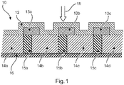
- Fig. 1 shows schematically and exemplarily an embodiment of a radiation detector 10 according to the invention. More specifically, Fig. 1 shows a section of a radiation detector comprising a small number of scintillator pixels. The skilled person understands that radiation detectors with large numbers of scintillator pixels may be obtained by continuing the structure depicted in Fig. 1 .
- the radiation detector 10 comprises a read-out sensor array 16, a first scintillator structure, a second scintillator structure and a coating 12.
- the first scintillator structure of the radiation detector 10 comprises a plurality of first scintillator pixels 14a, 14b, 14c and 14d, which are separated by gaps 15a, 15b and 15c.
- the first scintillator pixels 14a, 14b, 14c and 14d may comprise ceramic scintillator material or particle-in-binder scintillator material.
- the gaps 15a, 15b and 15c between the first scintillator pixels may be filled at least partially with a reflective material so that light cannot propagate between first scintillator pixels.
- the second scintillator structure of the radiation detector 10 comprises second scintillator pixels 13a, 13b and 13c.
- the second scintillator pixels 13a, 13b and 13c are optically coupled to the first scintillator pixels 14b, 14c and 14d, respectively.
- light can propagate between first and second scintillator pixels.
- the second scintillator pixels 13a, 13b and 13c overlap the gaps 15a, 15b and 15c between first scintillator pixels, respectively.
- the second scintillator pixels 13a, 13b and 13c absorb radiation, which may otherwise fall onto a gap 15a, 15b and 15c, respectively.
- the gaps between the first scintillator pixels are insensitive to radiation.
- the second scintillator pixels lead to an increased absorption of radiation, which corresponds to an increased scintillator fill factor.
- the second scintillator pixels may comprise ceramic scintillator material or particle-in-binder scintillator material.
- the second scintillator pixels may comprise a different scintillator material than the first scintillator pixels.
- the first scintillator pixels may comprise a ceramic scintillator material, and the second scintillator pixels may be mounted onto the first scintillator structure by means of additive manufacturing using particle-in-binder scintillator material.
- the radiation first propagates through the coating 12. Then, the radiation may be converted to light in the first scintillator pixels 14a, 14b, 14c or 14d or the second scintillator pixels 13a, 13b or 13c.
- the light emitted by scintillator material may be detected by the read-out sensor array 16, which comprises a plurality of light-sensitive sensor pixels.
- the coating 12 may be a light-reflective coating or a light-absorbing coating.
- a reflective coating 12 maybe adapted to reflect light, which may have been emitted by the scintillator material in a direction away from the read-out sensor array 16, back towards the read-out sensor array 16, so that it can be detected.
- an absorbing coating 12 may be adapted to absorb light, which may have been emitted by the scintillator material in a direction away from the read-out sensor array 16, so that it cannot propagate to distant light-sensitive sensor pixels.
- the second scintillator structure of Fig. 1 may result in a biased optical transfer function.
- radiation that would fall onto the gap 15a between first scintillator pixels 14a and 14b does not necessarily lead to the detection of light by the light-sensitive sensor pixel closest to the gap 15a.
- the second scintillator pixel 13a may absorb the radiation and emit light into the first scintillator pixel 14b.
- the light maybe detected by a light-sensitive sensor pixel that is further away from the light-sensitive sensor pixel closest to the gap 15a between the first scintillator pixels 14a and 14b.
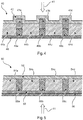
- Fig. 2 shows schematically and exemplarily another embodiment of a radiation detector 20 according to the invention. More specifically, Fig. 2 shows a section of a radiation detector comprising a small number of scintillator pixels. The skilled person understands that radiation detectors with large numbers of scintillator pixels may be obtained by continuing the structure depicted in Fig. 2 .
- the radiation detector 20 has a number of similarities to the radiation detector 10 depicted in Fig. 1 .
- the radiation detector 20 comprises a read-out sensor array 26, a first scintillator structure, a second scintillator structure and a coating 22.
- the first scintillator structure of the radiation detector 20 comprises a plurality of first scintillator pixels 24a, 24b, 24c and 24d, which are separated by gaps 25a, 25b and 25c.
- the first scintillator pixels 24a, 24b, 24c and 24d may comprise ceramic scintillator material or particle-in-binder scintillator material.
- the gaps 25a, 25b and 25c between the first scintillator pixels may be filled at least partially with a reflective material so that light cannot propagate between first scintillator pixels.
- the second scintillator structure of the radiation detector 20 comprises second scintillator pixels 23a, 23b and 23c.
- the second scintillator pixels 23a, 23b and 23c are optically coupled to the first scintillator pixels 24b, 24c and 24d, respectively, so that light can propagate between these first and second scintillator pixels.
- the second scintillator pixels 23a, 23b and 23c overlap the gaps 25a, 25b and 25c between first scintillator pixels, respectively.
- the second scintillator pixels 23 a, 23b and 23c result in an increased scintillator fill factor.
- the direction 21 from where radiation impinges on the radiation detector 20 is also shown.
- the radiation first propagates through the coating 22. Then, the radiation may be converted to light in the first scintillator pixels 24a, 24b, 24c or 24d or the second scintillator pixels 23a, 23b or 23c.
- the light emitted by scintillator material of the first or second scintillator structures may be detected by the read-out sensor array 26, which comprises a plurality of light-sensitive sensor pixels.
- the surfaces of the second scintillator pixels 23a, 23b and 23c comprise slanted surface sections 27a, 27b and 27c, respectively, which are inclined relative to the layer formed by the first scintillator structure.
- the slanted surface sections 27a, 27b and 27 are inclined to increase the probability that rays of light are reflected towards the first scintillator pixels.
- the angle between the slanted surface sections 27a, 27b and 27c and the layer formed by the first scintillator structure may typically lie in the range from 30° to 60°, but other angles are possible as well.
- Fig. 3 shows schematically and exemplarily another embodiment of a radiation detector 30 according to the invention. More specifically, Fig. 3 shows a section of a radiation detector comprising a small number of scintillator pixels. The skilled person understands that radiation detectors with large numbers of scintillator pixels may be obtained by continuing the structure depicted in Fig. 3 .
- the radiation detector 30 has a number of similarities to the radiation detector 10 depicted in Fig. 1 .
- the radiation detector 30 comprises a read-out sensor array 36, a first scintillator structure, a second scintillator structure and a coating 32.
- the first scintillator structure of the radiation detector 30 comprises a plurality of first scintillator pixels 34a, 34b, 34c and 34d, which are separated by gaps 35a, 35b and 35c.
- the first scintillator pixels 34a, 34b, 34c and 34d may comprise ceramic scintillator material or particle-in-binder scintillator material.
- the gaps 35a, 35b and 35c between the first scintillator pixels may be filled at least partially with a reflective material so that light cannot propagate between first scintillator pixels.
- the second scintillator structure of the radiation detector 30 comprises second scintillator pixels 33a, 33b and 33c.
- the second scintillator pixels 33a, 33b and 33c are optically coupled to the first scintillator pixels 34b, 34c and 34d, respectively, so that light can propagate between first and second scintillator pixels.
- the second scintillator pixels 33a, 33b and 33c overlap the gaps 35a, 35b and 35c between first scintillator pixels, respectively.
- the second scintillator pixels 33a, 33b and 33c result in an increased scintillator fill factor.
- the direction 31 from where radiation impinges on the radiation detector 30 is also shown.
- the radiation first propagates through the coating 32. Then, the radiation may be converted to light in the first scintillator pixels or the second scintillator pixels.
- the light emitted by the scintillator pixels may be detected by the read-out sensor array 36, which comprises a plurality of light-sensitive sensor pixels.
- Fig. 3 illustrates that the second scintillator pixels 33a, 33b and 33c are tilted relative to the layer formed by the first scintillator structure.
- the second scintillator pixels are tilted to increase the gaps between the second scintillator pixels 33a, 33b and 33c and the first scintillator pixels 34a, 34b and 34c, respectively.
- the gaps between these scintillator pixels are filled with the material of the coating 36, which results in an improved optical separation of the second scintillator pixels 33a, 33b and 33c from the first scintillator pixels 34a, 34b and 34c, respectively.
- the tilt of, for example, the second scintillator pixel 33a therefore ensures that the light emitted by the scintillator material of this pixel does not propagate to the first scintillator pixel 34a.
- the optical coupling of each of the second scintillator pixels to exactly one first scintillator pixel provides a high spatial resolution capability, but it may also lead to a biased image distortions.
- Fig. 4 shows schematically and exemplarily another embodiment of a radiation detector 40 according to the invention. More specifically, Fig. 4 shows a section of a radiation detector comprising a small number of scintillator pixels. The skilled person understands that radiation detectors with large numbers of scintillator pixels may be obtained by continuing the structure depicted in Fig. 4 .
- the radiation detector 40 has a number of similarities to the radiation detector 10 depicted in Fig. 1 .
- the radiation detector 40 comprises a read-out sensor array 46, a first scintillator structure, a second scintillator structure and a coating 42.
- the first scintillator structure of the radiation detector 40 comprises a plurality of first scintillator pixels 44a, 44b, 44c and 44d, which are separated by gaps 45a, 45b and 45c.
- the first scintillator pixels 44a, 44b, 44c and 44d may comprise ceramic scintillator material or particle-in-binder scintillator material.
- the gaps 45a, 45b and 45c between the first scintillator pixels may be filled at least partially with a reflective material so that light cannot propagate between first scintillator pixels.
- the second scintillator structure of the radiation detector 40 comprises second scintillator pixels 43a, 43b and 43c.
- the second scintillator pixels 43a, 43b and 43c are optically coupled to the first scintillator pixels, so that light can propagate between first and second scintillator pixels.
- the second scintillator pixels 43a, 43b and 43c overlap the gaps 45a, 45b and 45c between first scintillator pixels, respectively.
- the second scintillator pixels 43a, 43b and 43c result in an increased scintillator fill factor.
- the direction 41 from where radiation impinges on the radiation detector 40 is also shown.
- the radiation first propagates through the coating 42. Then, the radiation may be converted to light in the first scintillator pixels or the second scintillator pixels.
- the light emitted by the scintillator pixels may be detected by the read-out sensor array 46, which comprises a plurality of light-sensitive sensor pixels.
- Each of the second scintillator pixels 43a, 43b and 43c is optically coupled to the two adjacent first scintillator pixels.
- the second scintillator pixel 43a is optically coupled to the first scintillator pixels 44a and 44b.
- the second scintillator pixel 43b is optically coupled to the first scintillator pixels 44b and 44c.
- the second scintillator pixel 43c is optically coupled to the first scintillator pixels 44c and 44d. Optically coupling the second scintillator pixels to the adjacent first scintillator pixels may facilitate a simplified manufacturing of the radiation detector.
- optically coupling each of the second scintillator pixels to the adjacent first scintillator pixels may provide unbiased image distortions if light is fed from each of the second scintillator pixels into the first scintillator pixels adjacent to the second scintillator pixel with equal probabilities.
- optically coupling the second scintillator pixels to the adjacent first scintillator pixels may result in a reduced spatial resolution capability as compared to optically coupling each of the second scintillator pixels to exactly one of the adjacent first scintillator pixels.
- Fig. 5 shows schematically and exemplarily another embodiment of a radiation detector 50 according to the invention. More specifically, Fig. 5 shows a section of a radiation detector comprising a small number of scintillator pixels. The skilled person understands that radiation detectors with large numbers of scintillator pixels may be obtained by continuing the structure depicted in Fig. 5 .
- the radiation detector 50 comprises a read-out sensor array 56, a first scintillator structure, a second scintillator structure 53 and a coating 52.
- the first scintillator structure of the radiation detector 50 comprises a plurality of first scintillator pixels 54a, 54b, 54c and 54d, which are separated by gaps 55a, 55b and 55c.
- the first scintillator pixels 54a, 54b, 54c and 54d may comprise ceramic scintillator material or particle-in-binder scintillator material.
- the gaps 55a, 55b and 55c between the first scintillator pixels maybe filled at least partially with a reflective material so that light cannot propagate between first scintillator pixels.
- the second scintillator structure 53 of the radiation detector 50 is a non-pixelated slab scintillator.
- the second scintillator structure 53 is optically coupled to the first scintillator pixels, so that light can propagate between the first scintillator pixels and the second scintillator structure 53.
- the second scintillator structure 53 overlaps the gaps 55a, 55b and 55c between the first scintillator pixels.
- the second scintillator structure 53 results in an increased scintillator fill factor.
- the radiation first propagates through the read-out sensor array 56. Then, the radiation may be converted to light in the first scintillator pixels or the second scintillator structure. The emitted light may be detected by the read-out sensor array 56, which comprises a plurality of light-sensitive sensor pixels.
- a non-pixelated second scintillator structure maybe easy to manufacture. At the same time, a non-pixelated second scintillator structure may result in a reduced spatial resolution capability, since light may propagate through the whole non-pixelated second scintillator structure.
Landscapes
- Physics & Mathematics (AREA)
- Health & Medical Sciences (AREA)
- Spectroscopy & Molecular Physics (AREA)
- Molecular Biology (AREA)
- Life Sciences & Earth Sciences (AREA)
- General Physics & Mathematics (AREA)
- High Energy & Nuclear Physics (AREA)
- Engineering & Computer Science (AREA)
- Chemical & Material Sciences (AREA)
- Crystallography & Structural Chemistry (AREA)
- General Engineering & Computer Science (AREA)
- Biomedical Technology (AREA)
- General Health & Medical Sciences (AREA)
- Medical Informatics (AREA)
- Nuclear Medicine, Radiotherapy & Molecular Imaging (AREA)
- Optics & Photonics (AREA)
- Measurement Of Radiation (AREA)
Priority Applications (6)
| Application Number | Priority Date | Filing Date | Title |
|---|---|---|---|
| EP17206392.7A EP3495849A1 (en) | 2017-12-11 | 2017-12-11 | Multilayer pixelated scintillator with enlarged fill factor |
| EP18755206.2A EP3724690B1 (en) | 2017-12-11 | 2018-08-22 | Multilayer pixelated scintillator with enlarged fill factor |
| CN201880080154.2A CN111480095B (zh) | 2017-12-11 | 2018-08-22 | 具有增大填充因子的多层像素化闪烁体 |
| JP2020531661A JP7076549B2 (ja) | 2017-12-11 | 2018-08-22 | 高充填率を有するピクセル化された多層シンチレータ |
| PCT/EP2018/072636 WO2019115024A1 (en) | 2017-12-11 | 2018-08-22 | Multilayer pixelated scintillator with enlarged fill factor |
| US16/770,974 US11209556B2 (en) | 2017-12-11 | 2018-08-22 | Multilayer pixelated scintillator with enlarged fill factor |
Applications Claiming Priority (1)
| Application Number | Priority Date | Filing Date | Title |
|---|---|---|---|
| EP17206392.7A EP3495849A1 (en) | 2017-12-11 | 2017-12-11 | Multilayer pixelated scintillator with enlarged fill factor |
Publications (1)
| Publication Number | Publication Date |
|---|---|
| EP3495849A1 true EP3495849A1 (en) | 2019-06-12 |
Family
ID=60654839
Family Applications (2)
| Application Number | Title | Priority Date | Filing Date |
|---|---|---|---|
| EP17206392.7A Withdrawn EP3495849A1 (en) | 2017-12-11 | 2017-12-11 | Multilayer pixelated scintillator with enlarged fill factor |
| EP18755206.2A Active EP3724690B1 (en) | 2017-12-11 | 2018-08-22 | Multilayer pixelated scintillator with enlarged fill factor |
Family Applications After (1)
| Application Number | Title | Priority Date | Filing Date |
|---|---|---|---|
| EP18755206.2A Active EP3724690B1 (en) | 2017-12-11 | 2018-08-22 | Multilayer pixelated scintillator with enlarged fill factor |
Country Status (5)
| Country | Link |
|---|---|
| US (1) | US11209556B2 (https=) |
| EP (2) | EP3495849A1 (https=) |
| JP (1) | JP7076549B2 (https=) |
| CN (1) | CN111480095B (https=) |
| WO (1) | WO2019115024A1 (https=) |
Families Citing this family (4)
| Publication number | Priority date | Publication date | Assignee | Title |
|---|---|---|---|---|
| EP3835829A1 (en) * | 2019-12-09 | 2021-06-16 | Koninklijke Philips N.V. | X-ray detector |
| JP7835736B2 (ja) | 2020-09-02 | 2026-03-25 | ザ・リサーチ・ファウンデーション・フォー・ザ・ステイト・ユニヴァーシティ・オブ・ニューヨーク | テーパ付きシンチレータ結晶モジュールおよびそれを使用する方法 |
| KR20230082025A (ko) | 2020-10-07 | 2023-06-08 | 더 리서치 파운데이션 포 더 스테이트 유니버시티 오브 뉴욕 | 결정체-간 광이 공유되는 높은 분해능 비행-시간 양전자 방출 단층촬영 모듈들에 대한 전력-효율적 다중화를 위한 시스템 및 방법 |
| CN113555455B (zh) * | 2021-07-21 | 2023-12-19 | 北京京东方传感技术有限公司 | 平板探测器基板、制造方法、平板探测器及摄像设备 |
Citations (4)
| Publication number | Priority date | Publication date | Assignee | Title |
|---|---|---|---|---|
| EP1132754A2 (en) * | 2000-03-07 | 2001-09-12 | Marconi Medical Systems, Inc. | Scintillator for X-ray detector |
| US20070098138A1 (en) * | 2005-11-01 | 2007-05-03 | Koji Bessho | X-ray detector and x-ray ct apparatus |
| US20130048866A1 (en) * | 2011-08-26 | 2013-02-28 | Fujifilm Corporation | Radiation detector and radiological image radiographing apparatus |
| EP3018496A1 (en) * | 2014-11-06 | 2016-05-11 | General Equipment for Medical Imaging S.A. (Oncovision) | Hybrid scintillation module |
Family Cites Families (17)
| Publication number | Priority date | Publication date | Assignee | Title |
|---|---|---|---|---|
| US4560882A (en) * | 1984-08-31 | 1985-12-24 | Regents Of The University Of California | High-efficiency X-radiation converters |
| JPH01229995A (ja) * | 1988-03-10 | 1989-09-13 | Hamamatsu Photonics Kk | 放射線位置検出器 |
| US5208460A (en) | 1991-09-23 | 1993-05-04 | General Electric Company | Photodetector scintillator radiation imager having high efficiency light collection |
| CA2241779C (en) * | 1998-06-26 | 2010-02-09 | Ftni Inc. | Indirect x-ray image detector for radiology |
| US6891166B2 (en) | 2002-07-02 | 2005-05-10 | Ray Therapy Imaging Ab | Multi-layered radiation converter |
| AU2002953244A0 (en) * | 2002-12-10 | 2003-01-02 | Commonwealth Scientific And Industrial Research Organisation | A detection system |
| US6898265B1 (en) * | 2003-11-20 | 2005-05-24 | Ge Medical Systems Global Technology Company, Llc | Scintillator arrays for radiation detectors and methods of manufacture |
| US7308074B2 (en) * | 2003-12-11 | 2007-12-11 | General Electric Company | Multi-layer reflector for CT detector |
| US7260174B2 (en) | 2004-09-13 | 2007-08-21 | General Electric Company | Direct conversion energy discriminating CT detector with over-ranging correction |
| US7772558B1 (en) | 2006-03-29 | 2010-08-10 | Radiation Monitoring Devices, Inc. | Multi-layer radiation detector and related methods |
| US9917133B2 (en) * | 2013-12-12 | 2018-03-13 | General Electric Company | Optoelectronic device with flexible substrate |
| WO2016074945A1 (en) * | 2014-11-13 | 2016-05-19 | Koninklijke Philips N.V. | Pixelated scintillator with optimized efficiency |
| JP2016173267A (ja) | 2015-03-16 | 2016-09-29 | キヤノン株式会社 | 放射線検出装置、放射線検出システム並びにシンチレータ層の形成方法及び放射線検出装置の製造方法 |
| CN104820233B (zh) * | 2015-05-15 | 2019-03-01 | 中国科学院高能物理研究所 | 闪烁体阵列结构及应用该闪烁体阵列结构的中子探测器 |
| US9650569B1 (en) * | 2015-11-25 | 2017-05-16 | Siemens Medical Solutions Usa, Inc. | Method of manufacturing garnet interfaces and articles containing the garnets obtained therefrom |
| US10274610B2 (en) * | 2016-09-09 | 2019-04-30 | Minnesota Imaging And Engineering Llc | Structured detectors and detector systems for radiation imaging |
| EP3499272A1 (en) | 2017-12-14 | 2019-06-19 | Koninklijke Philips N.V. | Structured surface part for radiation capturing devices, method of manufacturing such a part and x-ray detector |
-
2017
- 2017-12-11 EP EP17206392.7A patent/EP3495849A1/en not_active Withdrawn
-
2018
- 2018-08-22 JP JP2020531661A patent/JP7076549B2/ja not_active Expired - Fee Related
- 2018-08-22 WO PCT/EP2018/072636 patent/WO2019115024A1/en not_active Ceased
- 2018-08-22 EP EP18755206.2A patent/EP3724690B1/en active Active
- 2018-08-22 US US16/770,974 patent/US11209556B2/en active Active
- 2018-08-22 CN CN201880080154.2A patent/CN111480095B/zh active Active
Patent Citations (4)
| Publication number | Priority date | Publication date | Assignee | Title |
|---|---|---|---|---|
| EP1132754A2 (en) * | 2000-03-07 | 2001-09-12 | Marconi Medical Systems, Inc. | Scintillator for X-ray detector |
| US20070098138A1 (en) * | 2005-11-01 | 2007-05-03 | Koji Bessho | X-ray detector and x-ray ct apparatus |
| US20130048866A1 (en) * | 2011-08-26 | 2013-02-28 | Fujifilm Corporation | Radiation detector and radiological image radiographing apparatus |
| EP3018496A1 (en) * | 2014-11-06 | 2016-05-11 | General Equipment for Medical Imaging S.A. (Oncovision) | Hybrid scintillation module |
Also Published As
| Publication number | Publication date |
|---|---|
| CN111480095B (zh) | 2024-11-08 |
| JP2021505896A (ja) | 2021-02-18 |
| JP7076549B2 (ja) | 2022-05-27 |
| EP3724690A1 (en) | 2020-10-21 |
| US20210165114A1 (en) | 2021-06-03 |
| EP3724690B1 (en) | 2024-04-24 |
| CN111480095A (zh) | 2020-07-31 |
| WO2019115024A1 (en) | 2019-06-20 |
| US11209556B2 (en) | 2021-12-28 |
Similar Documents
| Publication | Publication Date | Title |
|---|---|---|
| US4187427A (en) | Structure for collimated scintillation detectors useful in tomography | |
| US8304735B2 (en) | Radiation detecting apparatus and radiation detecting system | |
| US11209556B2 (en) | Multilayer pixelated scintillator with enlarged fill factor | |
| JP5011590B2 (ja) | 放射線位置検出器 | |
| US7772561B2 (en) | Apparatus and method for detecting an image | |
| US20090065700A1 (en) | Reduced edge effect detector | |
| CN102890284B (zh) | 一种核探测装置 | |
| WO2018223917A1 (zh) | 检测器和具有该检测器的发射成像设备 | |
| CN104838286A (zh) | 成像探测器 | |
| WO2019028205A1 (en) | DIGITAL X-RAY RADIOGRAPHY WITH ASYMMETRIC REFLECTIVE SCREENS | |
| US9864070B2 (en) | Scintillation detector | |
| JP4534006B2 (ja) | 放射線位置検出方法及び装置 | |
| US6671348B2 (en) | X-ray image detecting apparatus | |
| US7875855B2 (en) | Apparatus and method for detecting an image | |
| EP3428691A1 (en) | X-ray detector and method of manufacturing such a detector | |
| JP2003240857A (ja) | 放射線検出器 | |
| US11774606B2 (en) | Electromagnetic wave detector, electromagnetic wave detection apparatus, inspection apparatus, and circuit board | |
| JPH07311270A (ja) | 放射線検出器 | |
| CN114114374A (zh) | 一种闪烁体阵列及闪烁探测器 | |
| JP6516981B2 (ja) | 放射線検出器 | |
| RU197875U1 (ru) | Детектор рентгеновского излучения с составным сцинтиллятором | |
| CN111602247A (zh) | 有机感光器 | |
| JP2009047520A (ja) | X線画像検出パネル | |
| WO2020045229A1 (ja) | 放射線検出装置 | |
| JPH11248843A (ja) | 2次元アレイ型放射線検出器 |
Legal Events
| Date | Code | Title | Description |
|---|---|---|---|
| PUAI | Public reference made under article 153(3) epc to a published international application that has entered the european phase |
Free format text: ORIGINAL CODE: 0009012 |
|
| AK | Designated contracting states |
Kind code of ref document: A1 Designated state(s): AL AT BE BG CH CY CZ DE DK EE ES FI FR GB GR HR HU IE IS IT LI LT LU LV MC MK MT NL NO PL PT RO RS SE SI SK SM TR |
|
| AX | Request for extension of the european patent |
Extension state: BA ME |
|
| RAP1 | Party data changed (applicant data changed or rights of an application transferred) |
Owner name: KONINKLIJKE PHILIPS N.V. |
|
| STAA | Information on the status of an ep patent application or granted ep patent |
Free format text: STATUS: THE APPLICATION IS DEEMED TO BE WITHDRAWN |
|
| 18D | Application deemed to be withdrawn |
Effective date: 20191213 |