EP3495794A1 - Sensor chip, strain inducing body, and force sensor device - Google Patents
Sensor chip, strain inducing body, and force sensor device Download PDFInfo
- Publication number
- EP3495794A1 EP3495794A1 EP17858395.1A EP17858395A EP3495794A1 EP 3495794 A1 EP3495794 A1 EP 3495794A1 EP 17858395 A EP17858395 A EP 17858395A EP 3495794 A1 EP3495794 A1 EP 3495794A1
- Authority
- EP
- European Patent Office
- Prior art keywords
- beams
- detecting
- sensor chip
- force
- detecting beams
- Prior art date
- Legal status (The legal status is an assumption and is not a legal conclusion. Google has not performed a legal analysis and makes no representation as to the accuracy of the status listed.)
- Granted
Links
Images





















Classifications
-
- G—PHYSICS
- G01—MEASURING; TESTING
- G01L—MEASURING FORCE, STRESS, TORQUE, WORK, MECHANICAL POWER, MECHANICAL EFFICIENCY, OR FLUID PRESSURE
- G01L1/00—Measuring force or stress, in general
- G01L1/20—Measuring force or stress, in general by measuring variations in ohmic resistance of solid materials or of electrically-conductive fluids; by making use of electrokinetic cells, i.e. liquid-containing cells wherein an electrical potential is produced or varied upon the application of stress
- G01L1/22—Measuring force or stress, in general by measuring variations in ohmic resistance of solid materials or of electrically-conductive fluids; by making use of electrokinetic cells, i.e. liquid-containing cells wherein an electrical potential is produced or varied upon the application of stress using resistance strain gauges
- G01L1/2287—Measuring force or stress, in general by measuring variations in ohmic resistance of solid materials or of electrically-conductive fluids; by making use of electrokinetic cells, i.e. liquid-containing cells wherein an electrical potential is produced or varied upon the application of stress using resistance strain gauges constructional details of the strain gauges
- G01L1/2293—Measuring force or stress, in general by measuring variations in ohmic resistance of solid materials or of electrically-conductive fluids; by making use of electrokinetic cells, i.e. liquid-containing cells wherein an electrical potential is produced or varied upon the application of stress using resistance strain gauges constructional details of the strain gauges of the semi-conductor type
-
- G—PHYSICS
- G01—MEASURING; TESTING
- G01L—MEASURING FORCE, STRESS, TORQUE, WORK, MECHANICAL POWER, MECHANICAL EFFICIENCY, OR FLUID PRESSURE
- G01L1/00—Measuring force or stress, in general
- G01L1/20—Measuring force or stress, in general by measuring variations in ohmic resistance of solid materials or of electrically-conductive fluids; by making use of electrokinetic cells, i.e. liquid-containing cells wherein an electrical potential is produced or varied upon the application of stress
- G01L1/22—Measuring force or stress, in general by measuring variations in ohmic resistance of solid materials or of electrically-conductive fluids; by making use of electrokinetic cells, i.e. liquid-containing cells wherein an electrical potential is produced or varied upon the application of stress using resistance strain gauges
- G01L1/2206—Special supports with preselected places to mount the resistance strain gauges; Mounting of supports
- G01L1/2218—Special supports with preselected places to mount the resistance strain gauges; Mounting of supports the supports being of the column type, e.g. cylindric, adapted for measuring a force along a single direction
-
- G—PHYSICS
- G01—MEASURING; TESTING
- G01L—MEASURING FORCE, STRESS, TORQUE, WORK, MECHANICAL POWER, MECHANICAL EFFICIENCY, OR FLUID PRESSURE
- G01L5/00—Apparatus for, or methods of, measuring force, work, mechanical power, or torque, specially adapted for specific purposes
- G01L5/16—Apparatus for, or methods of, measuring force, work, mechanical power, or torque, specially adapted for specific purposes for measuring several components of force
- G01L5/161—Apparatus for, or methods of, measuring force, work, mechanical power, or torque, specially adapted for specific purposes for measuring several components of force using variations in ohmic resistance
- G01L5/162—Apparatus for, or methods of, measuring force, work, mechanical power, or torque, specially adapted for specific purposes for measuring several components of force using variations in ohmic resistance of piezoresistors
Definitions
- An approximate center part of the detecting beam 13a along a longitudinal direction, and an approximate center part of the opposing detecting beam 13b in the longitudinal direction, are connected by a detecting beam 13c for detecting the distortion, arranged perpendicularly to the detecting beam 13a and the detecting beam 13b.
- a detecting beam 13e is provided between the detecting beam 13d and the support part 11e, in parallel with respect to the detecting beam 13d and with a predetermined gap from each of the detecting beam 13d and the support beam 11e.
- the detecting beam 13e connects the end part of the reinforcing beam 12f on the side of the support part 11e, and an end part of the reinforcing beam 12g on the side of the support part 11e.
- the force application points 14a through 14d are points where the external force is applied, and may be formed by the BOX layer and the support layer of the SOI substrate, for example. Lower surfaces of the force application points 14a through 14d and lower surfaces of the support parts 11a through 11e respectively lie on approximately the same plane.
- parts forming inside corners are preferably rounded.
- FIG. 5 is a diagram for explaining signs of forces applied on each of axes and moments.
- a force in the X-axis direction is denoted by Fx
- a force in the Y-axis direction is denoted by Fy
- a force in the Z-axis direction is denoted by Fz.
- Mx a moment causing a rotation around the X-axis as a rotation axis
- My a moment causing a rotation around the Y-axis as the rotation axis
- Mz a moment causing a rotation around the Z-axis
- piezoresistive devices MzR1 and MzR2 are arranged closer to the detecting beam 13k than a bisector that bisects the detecting beam 13l along the lateral direction, at symmetrical positions with respect to the bisector that bisects the detecting beam 13l along the longitudinal direction.
- piezoresistive devices FzR1 and FzR2 are arranged on the bisector that bisects the detecting beam 131 along the longitudinal direction, at symmetrical positions with respect to the bisector that bisects the detecting beam 13l along the lateral direction.
- displacements (Fx, Fy, Mz) in the X-axis direction and the Y-axis direction can be detected based on the deformation of predetermined detecting beams.
- the forces (Fx, Fy) in the X-axis direction and the Y-axis direction can be detected based on the deformation of the detecting beams 13b, 13e, 13h, and 13k forming the second detecting beams.
- the moment (Mz) in the Z-axis direction can be detected based on the deformation of the detecting beams 13f and 13l forming the third detecting beams.
- FIG. 7 is a diagram illustrating an example of an electrode arrangement and wiring of the sensor chip 10, and is a plan view of the sensor chip 10 viewed from above in the Z-axis direction.
- the sensor chip 10 includes a plurality of electrodes 15 from which electrical signals are obtained.
- Each electrode 15 is arranged on the upper surface of the support parts 11a through 11d of the sensor chip 10 where the distortion is smallest when the force is applied to the force application points 14a through 14d.
- a wiring 16 from each piezoresistive device to the electrode 15 can be appropriately routed on each of the reinforcing beams and on each of the detecting beams.
- each of the reinforcing beams can also be used as a bypass if necessary when routing the wiring, it is possible to improve a degree of freedom of design of the wiring by arranging the reinforcing beams separately from the detecting beams. Hence, it is possible to arrange each of the piezoresistive devices at a more ideal position.
- 2 opposing piezoresistive devices have the same properties as the piezoresistive device MxR1 or the like used for the distortion detection.
- the other 2 opposing piezoresistive devices have properties different from the properties of the piezoresistive device MxR1 or the like by varying an impurity concentration using an impurity semiconductor. Hence, the temperature detection becomes possible because the bridge becomes imbalanced due to a temperature change.
- the flexure element 20 has a general shape that is a parallelepiped with a vertical length of approximately 5000 ⁇ m, a horizontal length of approximately 5000 ⁇ m, and a height of approximately 7000 ⁇ m, for example.
- a transverse cross section of each of the columns 22a through 22d may have a square shape with a side of approximately 1000 ⁇ m, for example.
- a transverse cross section of the column 22e may have a square shape with a side of approximately 2000 ⁇ m, for example.
- parts forming inside corners are preferably rounded.
- the sensor chip 10 is arranged while pressing the sensor chip 10 within the flexure element 20, so that the lower surface of the sensor chip 10 contacts the adhesive agent 41 that is coated on the upper surfaces of the columns 25a through 25e and the upper surfaces of the projecting parts 27a through 27d. Then, the adhesive agent 41 is heated to a predetermined temperature and cured. As a result, the sensor chip 10 is fixed within the flexure element 20. More particularly, the support parts 11a through 11d of the sensor chip 10 are fixed on the columns 25a through 25e, respectively, the support part 11e is fixed on the column 25e, and the force application points 14a through 14d are fixed on the projecting parts 27a through 27d, respectively.
- the piezoresistive devices FxR1 and FxR2 are positioned on the X1 side than the center along the longitudinal direction of the detecting beam 13k, the vertical tensile stress is generated to increase the resistance.
- the piezoresistive devices FxR3 and FxR4 are positioned on the X2 side than the center along the longitudinal direction of the detecting beam 13e, the vertical compressive stress is generated to decrease the resistance. Accordingly, a voltage is output from the bridge circuit illustrated in FIG. 16A because the piezoresistive devices FxR1 through FxR4 become imbalanced, to thereby enable detection of the force Fx.
- the piezoresistive devices are arranged on different detecting beams according to the kind of input to the piezoresistive devices.
- the sensitivity of an arbitrary axis can be adjusted independently by modifying the rigidity (thickness or width) of the corresponding detecting beam.
- the detecting beams 53a through 53l are provided on upper ends of the support parts 51a through 51e along the thickness direction, and may be formed by the active layer of the SOI substrate, for example. Sizes (widths along the lateral direction) of the detecting beams 53a through 53l may be approximately 150 ⁇ m, for example. Upper surfaces of the detecting beams 53a through 53l and the upper surfaces of the support parts 51a through 51e respectively lie on approximately the same plane. Thicknesses of the detecting beams 53a through 53l may be approximately 50 ⁇ m, for example.
- the force application point 54d is provided on the lower surface at the center part along the longitudinal direction of the detecting beam 53j (intersection of the detecting beam 53j and the detecting beam 53l).
- a set of detection block is formed by the detecting beams 53j, 53k, and 53l and the force application point 54d.
- the force application points 54a through 54d are points where the external force is applied, and may be formed by the BOX layer and the support layer of the SOI substrate, for example. Lower surfaces of the force application points 54a through 15d and lower surfaces of the support parts 51a through 51e respectively lie on approximately the same plane.
- piezoresistive devices MyR1 and MyR2 are arranged on a bisector that bisects the detecting beam 53j along the longitudinal direction, at symmetrical positions with respect to a bisector that bisects the detecting beam 53l along the longitudinal direction.
- piezoresistive devices FxR1 and FxR2 are arranged closer to the detecting beam 53j than an opening of the frame shaped detecting beam 13k, at symmetrical positions with respect to the bisector that bisects the detecting beam 53l along the longitudinal direction.
- a plurality of piezoresistive devices are separately arranged in each of the detection blocks, similarly as in the case of the sensor chip 10.
- the displacement in a predetermined axial direction can be detected in up to 6 axes at maximum, based on changes in outputs of the plurality of piezoresistive devices arranged on predetermined beams, according to the direction (axial direction) of the force or displacement applied (transmitted) to the force application points 54a through 54d, similarly as in the case of the sensor chip 10.
- the force-receiving plate 60 includes a main body 61 having an approximately circular shape, and 4 projecting parts 61a, 61b, 61c, and 61d provided on a lower surface side of the main body 61.
- the projecting part 61a contacts a region on the upper surface of the detecting beam 13a, and corresponding to the force application point 14a.
- the projecting part 61b contacts a region on the upper surface of the detecting beam 13j, and corresponding to the force application point 14d.
- the projecting part 61c contacts a region on the upper surface of the detecting beam 13g, and corresponding to the force application point 14c.
- the projecting part 61d contacts a region on the upper surface of the detecting beam 13d, and corresponding to the force application point 14b.
- a dicing may be performed in a state in which the sensor chip wafer is sandwiched between the glass wafer or the silicon wafer that becomes the column structure part 80 and the glass wafer that becomes the force-receiving plate 60, to simultaneously form the force-receiving plate 60, the sensor chip 10, and the column structure part 80.
- a basic beam structure of the sensor chip 110 is similar to that of the sensor chip 10.
- Support parts 111a through 111e of the sensor chip 110 corresponds to the support parts 11a through 11e of the sensor chip 10.
- widths of first detecting beams (detecting beams 113a, 113d, 113g, and 113j) and second detecting beams (detecting beams 113b, 113e, 113h, and 113k) are narrower than widths of third detecting beams (detecting beams 113c, 113f, 113i, and 113l).
- the detecting beam 113c has a length that is shorter (approximately 0.5 times).
- the detecting beam 113c has an average width that is approximately the same as that of the detecting beam 13c, however, differs from the detecting beam 13c in that the detecting beam 113c includes a part having a width that gradually decreases toward the side of the support part 111e.
- the detecting beams 113f, 113i, and 1131 have lengths that are shorter (approximately 0.5 times).
- the detecting beams 13f, 13i, and 131 have an average width that is approximately the same as that of the detecting beam 13c, however, differ from the detecting beam 13c in that the detecting beams 113f, 113i, and 1131 include a part having a width that gradually decreases toward the side of the support part 111e.
- the effects of making the detecting beams 113c, 113f, 113i, and 1131 short, and arranging the detecting beams 113b, 113e, 113h, and 113k close to the detecting beams 113a, 113d, 113g, and 113j, are large.
- the detecting beams 113b, 113e, 113h, and 113k can be made considerably narrower and longer compared to the detecting beams 13b, 13e, 13h, and 13k, to facilitate bending deformation and reduce stress concentration, and considerably improve the load capacity of the detecting beams 113b, 113e, 113h, and 113k.
- the piezoresistive devices MzR1 and MzR2 are arranged closer to the detecting beam 113k than the bisector that bisects the detecting beam 113j along the longitudinal direction, at symmetrical positions with respect to the bisector that bisects the detecting beam 1131 along the longitudinal direction in a region of the detecting beam 113j close to the detecting beam 1131.
- the maximum stress generated in the detecting beam of the sensor chip 110 can be made lower than or equal to that of the sensor chip 10.
- the beam width on a B-side of the detecting beam 113j (similarly for the detecting beams 113a, 113d, and 113g) illustrated in FIG. 29 is set to a width that is 75% to 80% of the beam width on an A-side, and the detecting beam 113j is tapered to decrease in width from the A-side toward the B-side, it is possible to improve the sensor sensitivity and simultaneously maintain the load capacity.
- the beam width on the B-side becomes 75% or less of the beam width on the A-side, the load capacity deteriorates and the beam becomes more easily damaged.
- the sensor sensitivity deteriorates.
Landscapes
- Physics & Mathematics (AREA)
- General Physics & Mathematics (AREA)
- Force Measurement Appropriate To Specific Purposes (AREA)
- Pressure Sensors (AREA)
- Micromachines (AREA)
Abstract
Description
- The present invention relates to a sensor chip, a flexure element, and a force sensor device.
- A force sensor device that is conventionally known includes a plurality of strain gauges that are bonded to a flexure element made of a metal, and detects multiaxial forces by converting a distortion, that occurs when an external force is applied, into an electrical signal. However, this force sensor device requires the strain gauges to be bonded one by one by manual operation, to thereby introduce problems from viewpoints of accuracy and productivity, and it is difficult to reduce the size of this force sensor device due to its structure.
- On the other hand, a force sensor device has been proposed that can eliminate the problem associated with the bonding accuracy and enable the size to be reduced, by replacing the strain gauge by a MEMS sensor chip for strain detection (for example, refer to Patent Document 1).
- Patent Document 1: Japanese Patent No.
4011345 - However, according to the force sensor device described above, an operation (signal processing) needs to be performed on outputs from a plurality of strain gauge elements of the sensor chip to obtain a 6-axis output, and a multiaxial output cannot be obtained by a simple method.
- The present invention is conceived in view of the above points, and one object of the present invention is to provide a sensor chip that can detect and output multiaxial displacements by a simple method.
- A disclosed sensor chip (10) is configured to detect a displacement in a predetermined axial direction in up to 6 axes at maximum, based on changes in outputs of a plurality of distortion detection devices arranged on predetermined beams, according to directions of forces or displacements applied to force application points, and includes a substrate; first support parts (11a through 11d) arranged at four corners of the substrate; a second support part (11e) arranged at a center of the substrate; first detecting beams (13a, 13d, 13g, 13j) respectively connecting adjacent first support parts (11a through 11d) to each other; second detecting beams (13b, 13e, 13h, 13k) respectively provided in parallel with respect to the first detecting beams (13a, 13d, 13g, 13j) between the respective first detecting beams (13a, 13d, 13g, 13j) and the second support part (11e); third detecting beams (13c, 13f, 13i, 131) connecting the first detecting beams (13a, 13d, 13g, 13j) and the second connecting beams (13b, 13e, 13h, 13k), in sets of the first detecting beams (13a, 13d, 13g, 13j) and the second detecting beams (13b, 13e, 13h, 13k) provided in parallel; force application points (14a through 14d), arranged at intersections of the first detecting beams (13a, 13d, 13g, 13j) and the third detecting beams (13c, 13f, 13i, 131), and applied with the forces; and a plurality of distortion detection devices (MxR1 through MxR4, MyR1 through MyR4, MzR1 through MzR4, FxR1 through FxR4, FyR1 through FyR4, FxR1 through FzR4) arranged at predetermined positions on the first detecting beams (13a, 13d, 13g, 13j), the second detecting beams (13b, 13e, 13h, 13k), and the third detecting beams (13f, 13l), wherein a displacement in a Z-axis direction along a thickness direction of the substrate is detected based on deformations of at least the third detecting beams (13f, 13l), and wherein displacements in an X-axis direction and a Y-axis direction respectively perpendicular to the Z-axis direction are detected based deformations of at least one of the first detecting beams (13a, 13d, 13g, 13j) and the second detecting beams (13b, 13e, 13h, 13k).
- Reference numerals in brackets above are added to facilitate understanding, and merely show examples, and are not limited to embodiments illustrated in the drawings.
- According to the disclosed technology, it is possible to provide a sensor chip that can detect and output multiaxial displacements by a simple method.
-
-
FIG. 1 is a perspective view illustrating an example of a force sensor device in a first embodiment. -
FIG. 2 is a perspective view illustrating an example of a sensor chip and a flexure element of the force sensor deice in the first embodiment. -
FIG. 3A is a diagram (part 1) of asensor chip 10 viewed from above in a Z-axis direction. -
FIG. 3B is a diagram (part 2) of thesensor chip 10 viewed from above in the Z-axis direction. -
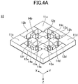
FIG. 4A is a diagram (part 1) of thesensor chip 10 viewed from below in the Z-axis direction. -
FIG. 4B is a diagram (part 2) of thesensor chip 10 viewed from below in the Z-axis direction. -
FIG. 5 is a diagram for explaining signs of forces applied on each of axes and moments. -
FIG. 6 is a diagram illustrating an example of an arrangement of piezoresistive devices of thesensor chip 10. -
FIG. 7 is a diagram illustrating an example of an electrode arrangement and wiring of thesensor chip 10. -
FIG. 8 is an enlarged plan view illustrating an example of a temperature sensor of thesensor chip 10. -
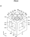
FIG. 9 is a perspective view illustrating an example of aflexure element 20. -
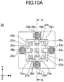
FIG. 10A is a diagram (part 1) illustrating the example of theflexure element 20. -
FIG. 10B is a diagram (part 2) illustrating the example of theflexure element 20. -
FIG. 11A is a diagram (part 1) illustrating an example of a manufacturing process of aforce sensor device 1. -
FIG. 11B is a diagram (part 2) illustrating the example of the manufacturing process of theforce sensor device 1. -
FIG. 12A is a diagram (part 3) illustrating the example of the manufacturing process of theforce sensor device 1. -
FIG. 12B is a diagram (part 4) illustrating the example of the manufacturing process of theforce sensor device 1. -
FIG. 13A is a diagram (part 5) illustrating the example of the manufacturing process of theforce sensor device 1. -
FIG. 13B is a diagram (part 6) illustrating the example of the manufacturing process of theforce sensor device 1. -
FIG. 14 is a simulation result (part 1) of deformation (distortion) when force and moment are applied to the flexure element. -
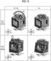
FIG. 15 is a simulation result (part 2) of the deformation (distortion) when the force and moment are applied to the flexure element. -
FIG. 16A is a simulation result (part 1) of stress generated in thesensor chip 10 when the force and moment ofFIG. 14 andFIG. 15 are applied. -
FIG. 16B is a simulation result (part 2) of the stress generated in thesensor chip 10 when the force and moment ofFIG. 14 andFIG. 15 are applied. -
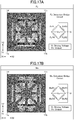
FIG. 17A is a simulation result (part 3) of the stress generated in thesensor chip 10 when the force and moment ofFIG. 14 andFIG. 15 are applied. -
FIG. 17B is a simulation result (part 4) of the stress generated in thesensor chip 10 when the force and moment ofFIG. 14 andFIG. 15 are applied. -
FIG. 18A is a simulation result (part 5) of the stress generated in thesensor chip 10 when the force and moment ofFIG. 14 andFIG. 15 are applied. -
FIG. 18B is a simulation result (part 6) of the stress generated in thesensor chip 10 when the force and moment ofFIG. 14 andFIG. 15 are applied. -
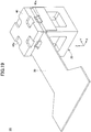
FIG. 19 is a perspective view illustrating an example of the force sensor device in amodification 1 of the first embodiment. -
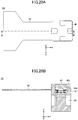
FIG. 20A is a diagram (part 1) illustrating the example of the force sensor device in themodification 1 of the first embodiment. -
FIG. 20B is a diagram (part 2) illustrating the example of the force sensor device in themodification 1 of the first embodiment. -
FIG. 21A is a diagram (part 1) of asensor chip 50 viewed from above in the Z-axis direction. -
FIG. 21B is a diagram (part 2) of thesensor chip 50 viewed from above in the Z-axis direction. -
FIG. 22 is a diagram illustrating an example of an arrangement of piezoresistive devices of thesensor chip 50. -
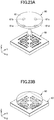
FIG. 23A is a perspective view (part 1) illustrating an example of the force sensor device in a modification 3 of the first embodiment. -
FIG. 23B is a perspective view (part 2) illustrating the example of the force sensor device in the modification 3 of the first embodiment. -
FIG. 23C is a perspective view (part 3) illustrating the example of the force sensor device in the modification 3 of the first embodiment. -
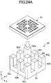
FIG. 24A is a perspective view (part 1) illustrating an example of the force sensor device in a modification 4 of the first embodiment. -
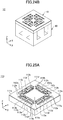
FIG. 24B is a perspective view (part 2) illustrating the example of the force sensor device in the modification 4 of the first embodiment. -
FIG. 25A is a diagram (part 1) of asensor chip 110 viewed from above in the Z-axis direction. -
FIG. 25B is a diagram (part 2) of thesensor chip 110 viewed from above in the Z-axis direction. -
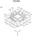
FIG. 26A is a diagram (part 1) of thesensor chip 110 viewed from below in the Z-axis direction. -
FIG. 26B is a diagram (part 2) of thesensor chip 110 viewed from below in the Z-axis direction. -
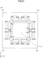
FIG. 27 is a diagram illustrating an example of an arrangement of piezoresistive devices of thesensor chip 110. -
FIG. 28A is a diagram (part 1) for explaining an improvement of load capacity of thesensor chip 110. -
FIG. 28B is a diagram (part 2) for explaining the improvement of the load capacity of thesensor chip 110. -
FIG. 29 is a diagram (part 3) for explaining the improvement of the load capacity of thesensor chip 110. -
FIG. 30A is a diagram (part 4) for explaining the improvement of the load capacity of thesensor chip 110. -
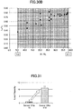
FIG. 30B is a diagram (part 5) for explaining the improvement of the load capacity of thesensor chip 110. -
FIG. 31 is a diagram (part 6) for explaining the improvement of the load capacity of thesensor chip 110. -
FIG. 32A is a diagram (part 1) for explaining an improvement of sensitivity of thesensor chip 110. -
FIG. 32B is a diagram (part 2) for explaining the improvement of the sensitivity of thesensor chip 110. -
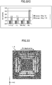
FIG. 32C is a diagram (part 3) for explaining the improvement of the sensitivity of thesensor chip 110. -
FIG. 33 is a diagram (part 1) for explaining an improvement of other axial properties of thesensor chip 110. -
FIG. 34A is a diagram (part 2) for explaining the improvement of the other axial properties of thesensor chip 110. -
FIG. 34B is a diagram (part 3) for explaining the improvement of the other axial properties of thesensor chip 110. -
FIG. 35A is a simulation result (part 1) of stress generated in thesensor chip 110 when the force and moment are applied. -
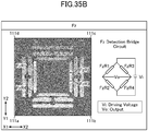
FIG. 35B is the simulation result (part 2) of the stress generated in thesensor chip 110 when the force and moment are applied. -
FIG. 36A is the simulation result (part 3) of the stress generated in thesensor chip 110 when the force and moment are applied. -
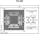
FIG. 36B is the simulation result (part 4) of the stress generated in thesensor chip 110 when the force and moment are applied. - Embodiments of the present invention will be described hereunder, by referring to the drawings. In each of the figures, identical constituent parts are designated by identical reference numerals, and repeated description of the same constituent parts may be omitted.
-
FIG. 1 is a perspective view illustrating an example of a force sensor device in a first embodiment.FIG. 2 is a perspective view illustrating an example of a sensor chip and a flexure element of the force sensor deice in the first embodiment. As illustrated inFIG. 1 andFIG. 2 , aforce sensor device 1 includes asensor chip 10, aflexure element 20, and an input andoutput substrate 30. Theforce sensor device 1 is a multiaxial force sensor device that is mounted on an arm, a finger, or the like of a robot that is used by machine tools or the like, for example. - The
sensor chip 10 is bonded to an upper surface of theflexure element 20 so as not to project from theflexure element 20. In addition, one end of the input andoutput substrate 30 that inputs and outputs signals with respect to thesensor chip 10 is bonded to the upper surface and side surfaces of theflexure element 20. Thesensor chip 10 and eachelectrode 31 of the input andoutput substrate 30 are electrically connected by a bonding wire or the like (not illustrated). Terminals (not illustrated), that can make electrical input and output with respect to a control device or the like connected to theforce sensor device 1, are arranged on the other end of the input andoutput substrate 30. - For the sake of convenience in this embodiment, in the
force sensor device 1, the side of the flexure element 2 provided with the input andoutput substrate 30 will be referred to as an upper side or one side, and an opposite side of the flexure element 2 will be referred to as a lower side or the other side. Further, in each part, a surface on the side of the flexure element 2 provided with the input andoutput substrate 30 will be referred to as one surface or an upper surface, and a surface on the opposite side of the flexure element 2 will be referred to as the other surface of a lower surface. However, theforce sensor device 1 may be used in an up-side-down state, or may be arranged at an arbitrary inclination angle. In addition, a plan view of a target part indicates a view in a normal direction (Z-axis direction) to the upper surface of thesensor chip 10, and a planar shape of the target part indicates a shape when viewed in the normal direction (Z-axis direction) to the upper surface of thesensor chip 10. -
FIG. 3A is a perspective view of thesensor chip 10 viewed from above in the Z-axis direction, andFIG. 3B is a plan view of thesensor chip 10 viewed from above in the Z-axis direction.FIG. 4A is a perspective view of thesensor chip 10 viewed from below in the Z-axis direction, andFIG. 4B is a bottom view of thesensor chip 10 viewed from below in the Z-axis direction. For the sake of convenience, surfaces having the same height inFIG. 4B are indicated by the same dot pattern. A direction parallel to one side of the upper surface of thesensor chip 10 is an X-axis direction, a direction perpendicular to the one side of the upper surface of thesensor chip 10 is a Y-axis direction, and a thickness direction of the sensor chip 10 (normal direction to the upper surface of the sensor chip 10) is the Z-axis direction. The X-axis direction, the Y-axis direction, and the Z-axis direction are perpendicular to each other. - The
sensor chip 10 illustrated inFIG. 3A, FIG. 3B ,FIG. 4A , andFIG. 4B is a MEMS (Micro Electro Mechanical Systems) sensor chip capable of detection in up to 6 axes at maximum by a single chip, and is formed on a semiconductor substrate such as a SOI (Silicon On Insulator) substrate or the like. The planar shape of thesensor chip 10 may be a square shape having a side of approximately 3000 µm, for example. - The
sensor chip 10 includes 5columnar support parts 11a through 11e. The planar shape of thesupport parts 11a through 11e may be a square shape having a side of approximately 500 µm, for example. Thesupport parts 11a through 11d forming first support parts are arranged at four corners of thesensor chip 10. Thesupport part 11e forming a second support part is arranged at a center of thesupport parts 11a through 11d. - The
support parts 11a through 11e may be formed by an active layer, a BOX layer, and a support layer of the SOI substrate, for example, and thicknesses of thesupport parts 11a through 11e may be approximately 500 µm, for example. - A reinforcing
beam 12a for structural reinforcement, having both ends thereof respectively fixed to thesupport part 11a and thesupport part 11b (connecting the adjacent support parts), is provided between thesupport part 11a and thesupport part 11b. A reinforcingbeam 12b for structural reinforcement, having both ends thereof respectively fixed to thesupport part 11b and thesupport part 11c (connecting the adjacent support parts), is provided between thesupport part 11b and thesupport part 11c. - A reinforcing
beam 12c for structural reinforcement, having both ends thereof respectively fixed to thesupport part 11c and thesupport part 11d (connecting the adjacent support parts), is provided between thesupport part 11c and thesupport part 11d. A reinforcingbeam 12d for structural reinforcement, having both ends thereof respectively fixed to thesupport part 11d and thesupport part 11a (connecting the adjacent support parts), is provided between thesupport part 11d and thesupport part 11a. - In other words, the 4 reinforcing
beams support parts - The corner part on an inner side of the
support part 11a and an opposing corner part of thesupport part 11e are connected by a reinforcingbeam 12e for structural reinforcement. The corner part on an inner side of thesupport part 11b and an opposing corner part of thesupport part 11e are connected by a reinforcingbeam 12f for structural reinforcement. - The corner part on an inner side of the
support part 11c and an opposing corner part of thesupport part 11e are connected by a reinforcingbeam 12g for structural reinforcement. The corner part on an inner side of thesupport part 11d and an opposing corner part of thesupport part 11e are connected by a reinforcingbeam 12h for structural reinforcement. The reinforcingbeams 12e through 12h forming second reinforcing beams are arranged obliquely with respect to the X-axis direction (Y-axis direction). In other words, the reinforcingbeams 12e through 12h are arranged non-parallel with respect to the reinforcingbeams - The reinforcing
beams 12a through 12h may be formed by the active layer, the BOX layer, and the support layer of the SOI substrate, for example. Sizes (widths along a lateral direction) of the reinforcingbeams 12a through 12h may be approximately 140 µm, for example. Upper surfaces of the reinforcingbeams 12a through 12h and upper surfaces of thesupport parts 11a through 11e respectively lie on approximately the same plane. - On the other hand, lower surfaces of the reinforcing
beams 12a through 12h respectively cave in from lower surfaces of thesupport parts 11a through 11e and lower surfaces of force application points 14a through 14d by approximately several tens of µm toward the upper surfaces of the reinforcingbeams 12a through 12h. Such caved-in structures prevent the lower surfaces of the reinforcingbeams 12a through 12h from contacting an opposing surface of theflexure element 20, when bonding thesensor chip 10 on theflexure element 20. - By arranging, separately from detecting beams for detecting the distortion, the reinforcing beams that are thicker and more rigid than the detecting beams, it is possible to increase the rigidity of the
entire sensor chip 10. Accordingly, parts other than the detecting beams are uneasily deformed in response to the input, to make it possible to obtain satisfactory sensor properties. - A detecting
beam 13a for detecting the distortion, having both ends thereof respectively fixed to thesupport part 11a and thesupport part 11b (connecting the adjacent support parts), is provided on an inner side of the reinforcingbeam 12a between thesupport part 11a and thesupport part 11b, in parallel with respect to the reinforcingbeam 12a and with a predetermined gap from the reinforcingbeam 12a. - A detecting
beam 13b is provided between the detectingbeam 13a and thesupport part 11e, in parallel with respect to the detectingbeam 13a and with a predetermined gap from each of the detectingbeam 13a and thesupport beam 11e. The detectingbeam 13b connects an end part of the reinforcingbeam 12e on the side of thesupport part 11e, and an end part of the reinforcingbeam 12f on the side of thesupport part 11e. - An approximate center part of the detecting
beam 13a along a longitudinal direction, and an approximate center part of the opposing detectingbeam 13b in the longitudinal direction, are connected by a detectingbeam 13c for detecting the distortion, arranged perpendicularly to the detectingbeam 13a and the detectingbeam 13b. - A detecting
beam 13d for detecting the distortion, having both ends thereof respectively fixed to thesupport part 11b and thesupport part 11c (connecting the adjacent support parts), is provided on an inner side of the reinforcingbeam 12b between thesupport part 11b and thesupport part 11c, in parallel with respect to the reinforcingbeam 12b and with a predetermined gap from the reinforcingbeam 12b. - A detecting
beam 13e is provided between the detectingbeam 13d and thesupport part 11e, in parallel with respect to the detectingbeam 13d and with a predetermined gap from each of the detectingbeam 13d and thesupport beam 11e. The detectingbeam 13e connects the end part of the reinforcingbeam 12f on the side of thesupport part 11e, and an end part of the reinforcingbeam 12g on the side of thesupport part 11e. - An approximate center part of the detecting
beam 13d along the longitudinal direction, and an approximate center part of the opposing detectingbeam 13e in the longitudinal direction, are connected by a detectingbeam 13f for detecting the distortion, arranged perpendicularly to the detectingbeam 13d and the detectingbeam 13e. - A detecting
beam 13g for detecting the distortion, having both ends thereof respectively fixed to thesupport part 11c and thesupport part 11d (connecting the adjacent support parts), is provided on an inner side of the reinforcingbeam 12c between thesupport part 11c and thesupport part 11d, in parallel with respect to the reinforcingbeam 12c and with a predetermined gap from the reinforcingbeam 12c. - A detecting
beam 13h is provided between the detectingbeam 13g and thesupport part 11e, in parallel with respect to the detectingbeam 13g and with a predetermined gap from each of the detectingbeam 13g and thesupport beam 11e. The detectingbeam 13h connects the end part of the reinforcingbeam 12g on the side of thesupport part 11e, and an end part of the reinforcingbeam 12h on the side of thesupport part 11e. - An approximate center part of the detecting
beam 13g along the longitudinal direction, and an approximate center part of the opposing detectingbeam 13h in the longitudinal direction, are connected by a detectingbeam 13i for detecting the distortion, arranged perpendicularly to the detectingbeam 13g and the detectingbeam 13h. - A detecting
beam 13i for detecting the distortion, having both ends thereof respectively fixed to thesupport part 11d and thesupport part 11a (connecting the adjacent support parts), is provided on an inner side of the reinforcingbeam 12d between thesupport part 11d and thesupport part 11a, in parallel with respect to the reinforcingbeam 12d and with a predetermined gap from the reinforcingbeam 12d. - A detecting
beam 13k is provided between a detectingbeam 13j and thesupport part 11e, in parallel with respect to the detectingbeam 13j and with a predetermined gap from each of the detectingbeam 13j and thesupport beam 11e. The detectingbeam 13k connects the end part of the reinforcingbeam 12h on the side of thesupport part 11e, and the end part of the reinforcingbeam 12e on the side of thesupport part 11e. - An approximate center part of the detecting
beam 13j along the longitudinal direction, and an approximate center part of the opposing detectingbeam 13k in the longitudinal direction, are connected by a detecting beam 13l for detecting the distortion, arranged perpendicularly to the detectingbeam 13j and the detectingbeam 13k. - The detecting
beams 13a through 13l are provided on upper ends of thesupport parts 11a through 11e along the thickness direction, and may be formed by the active layer of the SOI substrate, for example. Sizes (widths along the lateral direction) of the detectingbeams 13a through 13l may be approximately 75 µm, for example. Upper surfaces of the detectingbeams 13a through 13l and the upper surfaces of thesupport parts 11a through 11e respectively lie on approximately the same plane. Thicknesses of the detectingbeams 13a through 13l may be approximately 50 µm, for example. - The
force application point 14a is provided on the lower surface at the center part along the longitudinal direction of the detectingbeam 13a (intersection of the detectingbeam 13a and the detectingbeam 13c). A set of detection block is formed by the detectingbeams force application point 14a. - The
force application point 14b is provided on the lower surface at the center part along the longitudinal direction of the detectingbeam 13d (intersection of the detectingbeam 13d and the detectingbeam 13f). A set of detection block is formed by the detectingbeams force application point 14b. - The
force application point 14c is provided on the lower surface at the center part along the longitudinal direction of the detectingbeam 13g (intersection of the detectingbeam 13g and the detectingbeam 13i). A set of detection block is formed by the detectingbeams force application point 14c. - The
force application point 14d is provided on the lower surface at the center part along the longitudinal direction of the detectingbeam 13j (intersection of the detectingbeam 13j and the detecting beam 131). A set of detection block is formed by the detectingbeams force application point 14d. - The force application points 14a through 14d are points where the external force is applied, and may be formed by the BOX layer and the support layer of the SOI substrate, for example. Lower surfaces of the force application points 14a through 14d and lower surfaces of the
support parts 11a through 11e respectively lie on approximately the same plane. - Accordingly, a different beam deformation is obtained for each kind of force, by inputting the force or the displacement from the 4 force application points 14a through 14d, and thus, it is possible to provide a sensor having satisfactory properties for isolating the 6 axes.
- From a viewpoint of reducing stress concentration in the
sensor chip 10, parts forming inside corners are preferably rounded. -
FIG. 5 is a diagram for explaining signs of forces applied on each of axes and moments. As illustrated inFIG. 5 , a force in the X-axis direction is denoted by Fx, a force in the Y-axis direction is denoted by Fy, and a force in the Z-axis direction is denoted by Fz. In addition, a moment causing a rotation around the X-axis as a rotation axis is denoted by Mx, a moment causing a rotation around the Y-axis as the rotation axis is denoted by My, and a moment causing a rotation around the Z-axis is denoted by Mz. -
FIG. 6 is a diagram illustrating an example of an arrangement of piezoresistive devices of thesensor chip 10. The piezoresistive devices are arranged at predetermined positions of the detection blocks respectively corresponding to the 4 force application points 14a through 14d. - More particularly, as illustrated in
FIG. 3A, FIG. 3B , andFIG. 6 , in the detection block corresponding to theforce application point 14a, piezoresistive devices MxR3 and MxR4 are arranged on a bisector that bisects the detectingbeam 13a along the longitudinal direction, at symmetrical positions with respect to a bisector that bisects the detectingbeam 13c along the longitudinal direction. In addition, piezoresistive devices FyR3 and FyR4 are arranged closer to the detectingbeam 13a than a bisector that bisects the detectingbeam 13b along the longitudinal direction, at symmetrical positions with respect to the bisector that bisects the detectingbeam 13c along the longitudinal direction. - Further, in the detection block corresponding to the
force application point 14b, piezoresistive devices MyR3 and MyR4 are arranged on a bisector that bisects the detectingbeam 13d along the longitudinal direction, at symmetrical positions with respect to a bisector that bisects the detectingbeam 13f along the longitudinal direction. In addition, piezoresistive devices FxR3 and FxR4 are arranged closer to the detectingbeam 13d than a bisector that bisects the detectingbeam 13e along the longitudinal direction, at symmetrical positions with respect to the bisector that bisects the detectingbeam 13f along the longitudinal direction. - Moreover, piezoresistive devices MzR3 and MzR4 are arranged closer to the detecting
beam 13e than a bisector that bisects the detectingbeam 13f along the lateral direction, at symmetrical positions with respect to the bisector that bisects the detectingbeam 13f along the longitudinal direction. In addition, piezoresistive devices FzR3 and FzR4 are arranged on the bisector that bisects the detectingbeam 13f along the longitudinal direction, at symmetrical positions with respect to the bisector that bisects the detectingbeam 13f along the lateral direction. - Further, in the detection block corresponding to the
force application point 14c, piezoresistive devices MxR1 and MxR2 are arranged on a bisector that bisects the detectingbeam 13g along the longitudinal direction, at symmetrical positions with respect to a bisector that bisects the detectingbeam 13i along the longitudinal direction. In addition, piezoresistive devices FyR1 and FyR2 are arranged closer to the detectingbeam 13g than a bisector that bisects the detectingbeam 13h along the longitudinal direction, at symmetrical positions with respect to the bisector that bisects the detectingbeam 13i along the longitudinal direction. - Moreover, in the detection block corresponding to the
force application point 14d, piezoresistive devices MyR1 and MyR2 are arranged on a bisector that bisects the detectingbeam 13j along the longitudinal direction, at symmetrical positions with respect to a bisector that bisects the detectingbeam 131 along the longitudinal direction. In addition, piezoresistive devices FxR1 and FxR2 are arranged closer to the detectingbeam 13j than a bisector that bisects the detectingbeam 13k along the longitudinal direction, at symmetrical positions with respect to the bisector that bisects the detecting beam 13l along the longitudinal direction. - Further, piezoresistive devices MzR1 and MzR2 are arranged closer to the detecting
beam 13k than a bisector that bisects the detecting beam 13l along the lateral direction, at symmetrical positions with respect to the bisector that bisects the detecting beam 13l along the longitudinal direction. In addition, piezoresistive devices FzR1 and FzR2 are arranged on the bisector that bisects the detectingbeam 131 along the longitudinal direction, at symmetrical positions with respect to the bisector that bisects the detecting beam 13l along the lateral direction. - The piezoresistive devices FxR1 through FxR4 detect the force Fx, the piezoresistive devices FyR1 through FyR4 detect the force Fy, and the piezoresistive devices FzR1 through FzR4 detect the force Fz. In addition, the piezoresistive devices MxR1 through MxR4 detect the moment Mx, the piezoresistive devices MyR1 through MyR4 detect the moment My, and the piezoresistive devices MzR1 through MzR4 detect the moment Mz.
- Accordingly, in the
sensor chip 10, a plurality of piezoresistive devices are separately arranged in each of the detection blocks. Hence, the displacement in a predetermined axial direction can be detected in up to 6 axes at maximum, based on changes in outputs of the plurality of piezoresistive devices arranged on predetermined beams, according to the direction (axial direction) of the force or displacement applied (transmitted) to the force application points 14a through 14d. - More particularly, in the
sensor chip 10, displacements (Mx, My, Fz) in the Z-axis direction can be detected based on the deformation of predetermined detecting beams. In other words, the moments (Mx, My) in the X-axis direction and the Y-axis direction can be detected based on the deformation of the detectingbeams beams 13f and 13l forming the third detecting beams. - Further, in the
sensor chip 10, displacements (Fx, Fy, Mz) in the X-axis direction and the Y-axis direction can be detected based on the deformation of predetermined detecting beams. In other words, the forces (Fx, Fy) in the X-axis direction and the Y-axis direction can be detected based on the deformation of the detectingbeams beams 13f and 13l forming the third detecting beams. - By varying the thickness and the width of each of the detecting beams, it is possible to make adjustments such as making detection sensitivities uniform, improving detection accuracy, or the like.
- Of course, it is possible to reduce the number of piezoresistive devices, so that the sensor chip can detect the displacement in the predetermined axial direction in 5 axes or less.
-
FIG. 7 is a diagram illustrating an example of an electrode arrangement and wiring of thesensor chip 10, and is a plan view of thesensor chip 10 viewed from above in the Z-axis direction. As illustrated inFIG. 7 , thesensor chip 10 includes a plurality ofelectrodes 15 from which electrical signals are obtained. Eachelectrode 15 is arranged on the upper surface of thesupport parts 11a through 11d of thesensor chip 10 where the distortion is smallest when the force is applied to the force application points 14a through 14d. Awiring 16 from each piezoresistive device to theelectrode 15 can be appropriately routed on each of the reinforcing beams and on each of the detecting beams. - Accordingly, because each of the reinforcing beams can also be used as a bypass if necessary when routing the wiring, it is possible to improve a degree of freedom of design of the wiring by arranging the reinforcing beams separately from the detecting beams. Hence, it is possible to arrange each of the piezoresistive devices at a more ideal position.
-
FIG. 8 is an enlarged plan view illustrating an example of a temperature sensor of thesensor chip 10. As illustrated inFIG. 7 andFIG. 8 , thesensor chip 10 is provided with atemperature sensor 17 for performing a temperature correction on the piezoresistive devices that are used for the distortion detection. Thetemperature sensor 17 has a structure in which 4 piezoresistive devices TR1, TR2, TR3, and TR4 are connected in a bridge connection. - Among the piezoresistive devices TR1, TR2, TR3, and TR4, 2 opposing piezoresistive devices have the same properties as the piezoresistive device MxR1 or the like used for the distortion detection. In addition, among the piezoresistive devices TR1, TR2, TR3, and TR4, the other 2 opposing piezoresistive devices have properties different from the properties of the piezoresistive device MxR1 or the like by varying an impurity concentration using an impurity semiconductor. Hence, the temperature detection becomes possible because the bridge becomes imbalanced due to a temperature change.
- All of the piezoresistive devices (MxR1 or the like) used for the distortion detection are arranged horizontally or perpendicularly to a crystal orientation of the semiconductor substrate (silicon or the like) forming the
sensor chip 10. For this reason, with respect to the same distortion, it is possible to obtain a larger resistance change, to improve a measurement accuracy of the applied force and the moment. - On the other hand, the piezoresistive devices TR1, TR2, TR3, and TR4 forming the
temperature sensor 17 are arranged at a 45 degree inclination with respect to the crystal orientation of the semiconductor substrate (silicon or the like) forming thesensor chip 10. For this reason, it is possible to reduce the resistance change with respect to stress, to enable accurate detection of only the temperature change. - Further, the
temperature sensor 17 is arranged on the upper surface of thesupport part 11a of thesensor chip 10, where the distortion is the smallest when the force is applied to the force application points 14a through 14d. Hence, it is possible to further reduce the resistance change with respect to the stress. - The piezoresistive device is a typical example of a distortion detection device used in the present invention.
-
FIG. 9 is a perspective view illustrating an example of theflexure element 20.FIG. 10A is a plan view illustrating theflexure element 20, andFIG. 10B is a perspective view of a cross section along a line A-A inFIG. 10A . For the sake of convenience, surfaces having the same height inFIG. 10A are indicated by the same dot pattern. - As illustrated in
FIG. 9 ,FIG. 10A , andFIG. 10B , in theflexure element 20, 4columns 22a through 22d forming first columns are arranged at four corners on abase 21, and 4beams 23a through 23d forming first beams and respectively connecting mutually adjacent columns are provided in a frame shape. In addition, acolumn 22e forming a second column is arranged at a center on thebase 21. Thecolumn 22e is used to fix thesensor chip 10, and is formed to a size and length respectively larger and shorter than those of thecolumns 22a through 22d. Thesensor chip 10 is fixed on thecolumn 22e so as not to project from upper surfaces of thecolumns 22a through 22d. - The
flexure element 20 has a general shape that is a parallelepiped with a vertical length of approximately 5000 µm, a horizontal length of approximately 5000 µm, and a height of approximately 7000 µm, for example. A transverse cross section of each of thecolumns 22a through 22d may have a square shape with a side of approximately 1000 µm, for example. A transverse cross section of thecolumn 22e may have a square shape with a side of approximately 2000 µm, for example. - A projecting part, that projects upward from a center part along the longitudinal direction of each of the
beams 23a through 23d, is provided on the upper surface of each of thebeams 23a through 23d at the center part along the longitudinal direction, and for example, cylinder shapedinput 24d are provided on the respective projecting parts. Theparts 24a troughinput parts 24a through 24d are parts where the external force is applied, and when the force is applied to theinput parts 24a through 24d, thebeams 23a through 23d and thecolumns 22a through 22d are deformed according to the applied force. - The
column 22e is isolated from thebeams 23a through 23d that are deformed by the applied force and thecolumns 22a through 22d that are deformed by the applied force. For this reason, thecolumn 22e does not move (is not deformed by the applied force) even when the force is applied to theinput parts 24a through 24d. - By providing the 4
input parts 24a through 24d, it is possible to improve the load capacity of thebeams 23a through 23d when compared to a structure including a single input part, for example. - 4
columns 25a through 25d forming third columns are arranged at four corners on the upper surface of thecolumn 22e, and acolumn 25e forming a fourth column is arranged at a center part on the upper surface of of thecolumn 22e. Thecolumns 25a through 25e are formed to the same height. - In other words, the upper surfaces of each of the
columns 25a through 25e are located on the same plane. The upper surface of each of thecolumns 22a through 25e forms a bonding part that is bonded to a lower surface of thesensor chip 10. Thecolumns 25a through 25e are isolated from thebeams 23a through 23d that are deformed by the applied force, and from thecolumns 22a through 22d that are deformed by the applied force, and thus, thecolumns 25a through 25e will not move even when the force is applied to theinput parts 24a through 24d (are not deformed by the applied force). -
Beams 26a through 26d, that respectively project toward an inner side along the horizontal direction from a medial surface of each of thebeams 23a through 23d, are provided at center parts along the longitudinal direction of the medial surfaces of thebeams 23a through 23d, respectively. Thebeams 26a through 26d form second beams that transmit the deformations of thebeams 23a through 23d and thecolumns 22a through 22d to thesensor chip 10. In addition, projectingparts 27a through 27d, that respectively project upward from a tip end side of an upper surface of each of thebeams 26a through 26d, are provided at the tip end side of the upper surfaces of thebeams 26a through 26d, respectively. - The projecting
parts 27a through 27d are formed to the same height. In other words, upper surfaces of the projectingparts 27a through 27d are located on the same plane. The upper surface of each of the projectingparts 27a through 27d forms a bonding part that is bonded to the lower surface of thesensor chip 10. Because thebeams 26a through 26d and the projectingparts 27a through 27d are connected to thebeams 23a through 23d that form movable parts, thebeams 26a through 26d and the projectingparts 27a through 27d are deformed according to the force applied to theinput parts 24a through 24d. - In a state in which no force is applied to the
input parts 24a through 24d, the upper surface of each of thecolumns 25a through 25e and the upper surface of each of the projectingparts 27a through 27d are located on the same plane. - In the
flexure element 20, from a viewpoint of securing rigidity and manufacturing with a high accuracy, it is preferable that thebase 21, thecolumns 22a through 22e, thebeams 23a through 23d, theinput parts 24a through 24d, thecolumns 25a through 25e, thebeams 26a through 26d, and the projectingparts 27a through 27d are respectively formed integrally. A material used for theflexure element 20 may be a hard metal material such as SUS (stainless steel) or the like, for example. It is particularly preferable to use SUS630, that is hard and has a high mechanical strength, for theflexure element 20. - As described above, the
flexure element 20 has a structure including the columns and the beams, similar to the structure of thesensor chip 10. For this reason, theflexure element 20 exhibits a different deformation in each of the 6 axes according to the applied force, and can thus transmit the deformations in the 6 axes with satisfactory isolation to thesensor chip 10. - In other words, the force applied to the
input parts 24a through 24d of theflexure element 20 is transmitted to thesensor chip 10 via thecolumns 22a through 22d, thebeams 23a through 23d, and thebeams 26a through 26d, to detect the displacement by thesensor chip 10. Further, in thesensor chip 10, it is possible to obtain the output of each axis from the bridge circuit, where one bridge circuit is provided for one axis. - From a viewpoint of reducing stress concentration in the
flexure element 20, parts forming inside corners are preferably rounded. -
FIG. 11A through FIG. 13B are diagrams illustrating an example of a manufacturing process of theforce sensor device 1. First, as illustrated inFIG. 11A , theflexure element 20 is manufactured. Theflexure element 20 may be integrally formed by molding, cutting, wire electric discharging, or the like, for example. The material used for theflexure element 20 may be the hard metal material such as the SUS (stainless steel) or the like, for example. It is particularly preferable to use the SUS630, that is hard and has the high mechanical strength, for theflexure element 20. In a case in which theflexure element 20 is manufactured by molding, metal grains and a resin forming a binder are poured into a metal mold and molded, for example, and a sintering is thereafter performed to evaporate the resin, to manufacture theflexure element 20 made of the metal. - Next, in the process illustrated in
FIG. 11B , adadhesive agent 41 is coated on the upper surfaces of thecolumns 25a through 25e, and on the upper surfaces of the projectingparts 27a through 27d. For example, an epoxy adhesive agent or the like may be used for theadhesive agent 41. From a viewpoint of enduring pressure with respect to the external force that is applied, theadhesive agent 41 preferably has a Young's modulus of 1 GPa or higher, and is formed to a thickness of 20 µm or less. - Next, in the process illustrated in
FIG. 12A , thesensor chip 10 is manufactured. Thesensor chip 10 may be manufactured by a known method that prepares a SOI substrate, for example, and performs an etching process (for example, reactive ion etching or the like) or the like on the prepared substrate. In addition, electrodes and wirings may be formed by depositing a metal layer made of copper or the like on the substrate surface by a sputtering process or the like, for example, and patterning the metal layer using photolithography. - Next, in the process illustrated in
FIG. 12B , thesensor chip 10 is arranged while pressing thesensor chip 10 within theflexure element 20, so that the lower surface of thesensor chip 10 contacts theadhesive agent 41 that is coated on the upper surfaces of thecolumns 25a through 25e and the upper surfaces of the projectingparts 27a through 27d. Then, theadhesive agent 41 is heated to a predetermined temperature and cured. As a result, thesensor chip 10 is fixed within theflexure element 20. More particularly, thesupport parts 11a through 11d of thesensor chip 10 are fixed on thecolumns 25a through 25e, respectively, thesupport part 11e is fixed on thecolumn 25e, and the force application points 14a through 14d are fixed on the projectingparts 27a through 27d, respectively. - Next, in the process illustrated in
FIG. 13A , anadhesive agent 42 is coated on the upper surfaces of thecolumns 22a through 22d. For example, an epoxy adhesive agent or the like may be used for theadhesive agent 42. Theadhesive agent 42 is used to fix the input andoutput substrate 30 on theflexure element 20, and no external force is applied thereto, and thus, a general-purposes adhesive may be used for theadhesive agent 42. - Next, in the process illustrated in
FIG. 13B , the input andoutput substrate 30 is prepared, and the input andoutput substrate 30 is arranged on theflexure element 20, so that a lower surface of the input andoutput substrate 30 contacts theadhesive agent 42 that is coated on the upper surfaces of thecolumns 22a through 22d. In addition, theadhesive agent 42 is heated to a predetermined temperature and cured while pressing the input andoutput substrate 30 towards theflexure element 20. As a result, the input andoutput substrate 30 is fixed on theflexure element 20. - The input and
output substrate 30 is fixed to theflexure element 20 so as to expose thesensor chip 10 and theinput parts 24a through 24d. Eachelectrode 31 of the input andoutput substrate 30 is preferably arranged on thecolumns 22a through 22d of theflexure element 20 where the distortion is smallest when the force is applied to theinput parts 24a through 24d. - Thereafter, parts (excluding input terminal side) of the input and
output substrate 30, protruding in the horizontal direction from theflexure element 20, are bend toward side surfaces of theflexure element 20. In addition, corresponding parts of the input andoutput substrate 30 and thesensor chip 10 are electrically connected by bonding wires or the like (not illustrated). As a result, theforce sensor device 1 illustrated inFIG. 1 is completed. - As described above, the
force sensor device 1 can be manufactured using only 3 components, namely, thesensor chip 10, theflexure element 20, and the input andoutput substrate 30, and for this reason, theforce sensor device 1 can be assembled with ease. Further, because locations requiring alignment can be reduced to a minimum, it is possible to reduce deterioration in the accuracy caused by mounting. - In addition, in the
flexure element 20, parts (the upper surfaces of thecolumns 25a through 25e, and the upper surfaces of the projectingparts 27a through 27d) connecting to thesensor chip 10 are all located on the same plane. Accordingly, the alignment of thesensor chip 10 with respect to theflexure element 20 is only required once, and thesensor chip 10 can be mounted on theflexure element 20 with ease. -
FIG. 14 andFIG. 15 are simulation results of deformation (distortion) when the force and moment are applied to theflexure element 20. The force and moment are applied from theinput part 24a through 24d (refer toFIG. 9 etc.) of theflexure element 20. In addition,FIG. 16A through FIG. 18B are simulation results of the stress generated in thesensor chip 10 when the force and moment ofFIG. 14 andFIG. 15 are applied. InFIG. 16A through FIG. 18B , a vertical tensile stress is indicated by "+", and a vertical compressive stress is indicated by "-". - In a case in which the force Fx is applied in a direction from X1 to X2 along the X-axis, the
flexure element 20 is deformed as illustrated inFIG. 14 , and the stress illustrated inFIG. 16A is generated in thesensor chip 10. More particularly, by applying the force Fx, the detectingbeams - Because the piezoresistive devices FxR1 and FxR2 are positioned on the X1 side than the center along the longitudinal direction of the detecting
beam 13k, the vertical tensile stress is generated to increase the resistance. On the other hand, because the piezoresistive devices FxR3 and FxR4 are positioned on the X2 side than the center along the longitudinal direction of the detectingbeam 13e, the vertical compressive stress is generated to decrease the resistance. Accordingly, a voltage is output from the bridge circuit illustrated inFIG. 16A because the piezoresistive devices FxR1 through FxR4 become imbalanced, to thereby enable detection of the force Fx. - The detecting
beams FIG. 18A . - In a case in which the force Fy is applied in a direction from Y1 to Y2 along the Y-axis, the stress illustrated in
FIG. 16B is generated in thesensor chip 10. More particularly, by applying the force Fy, the detectingbeams - Because the piezoresistive devices FyR3 and FyR4 are positioned on the Y1 side than the center along the longitudinal direction of the detecting
beam 13b, the vertical tensile stress is generated to increase the resistance. On the other hand, because the piezoresistive devices and FyR2 are positioned on the Y2 side than the center along the longitudinal direction of the detectingbeam 13h, the vertical compressive stress is generated to decrease the resistance. Accordingly, a voltage is output from the bridge circuit illustrated inFIG. 16B because the piezoresistive devices through FyR4 become imbalanced, to thereby enable detection of the force Fy. - For reasons similar to the bridge circuit of the moment My, no voltage is output from the bridge circuit of the moment Mx illustrated in
FIG. 17B . - In a case in which the force Fz is applied in a direction from Z1 to Z2 along the Z-axis, the
flexure element 20 is deformed as illustrated inFIG. 14 , and the stress illustrated inFIG. 17A is generated in thesensor chip 10. More particularly, by applying the force Fz, the detectingbeams - In this case, the vertical tensile stress is generated in the piezoresistive devices FzR1 and FzR4 to increase the resistance. In addition, the vertical compressive stress is generated in the piezoresistive devices FzR2 and FzR3 to decrease the resistance. Accordingly, the piezoresistive devices FzR1 through FzR4 become imbalanced, to thereby enable detection of the force Fz by the bridge circuit illustrated in
FIG. 17A . - For reasons similar to the above described, no voltage is output from the bridge circuit of the force Fx illustrated in
FIG. 16A , the bridge circuit of the force Fy illustrated inFIG. 16B , the bridge circuit of the moment Mx illustrated inFIG. 17B , the bridge circuit of the moment My illustrated inFIG. 18A , and the bridge circuit of the moment Mz illustrated inFIG. 18B . - In a case in which the moment Mx is applied in the direction of Y2-Z2-Y1 using the X-axis as the rotation axis, the stress illustrated in
FIG. 17B is generated in thesensor chip 10. More particularly, by applying the moment Mx, the detectingbeams FIG. 17B . - For reasons similar to the above described, no voltage is output from the bridge circuit of the force Fy illustrated in
FIG. 16B . - In a case in which the moment My is applied in the direction of X1-Z2-X2 using the Y-axis as the rotation axis, the
flexure element 20 is deformed as illustrated inFIG. 15 , and the stress illustrated inFIG. 18A is generated in thesensor chip 10. More particularly, by applying the moment My, the detectingbeams - In this case, the vertical tensile stress is generated in the piezoresistive devices MyR1 and MyR2 to increase the resistance. In addition, the vertical compressive stress is generated in the piezoresistive devices MyR3 and MyR4 to decrease the resistance. Accordingly, the piezoresistive devices MyR1 through MyR4 become imbalanced, to thereby enable detection of the moment My by the bridge circuit illustrated in
FIG. 18A . - For reasons similar to the above described, no voltage is output from the bridge circuit of the force Fx illustrated in
FIG. 16A . - In a case in which the moment Mz is applied in the direction of X2-Y2-X1 using the Z-axis as the rotation axis, the
flexure element 20 is deformed as illustrated inFIG. 15 , and the stress illustrated inFIG. 18B is generated in thesensor chip 10. More particularly, by applying the moment Mz, the detectingbeams - In this case, the vertical tensile stress is generated in the piezoresistive devices MzR1 and MzR4 to increase the resistance. In addition, the vertical compressive stress is generated in the piezoresistive devices MzR2 and MzR3 to decrease the resistance. Accordingly, the piezoresistive devices MzR1 through MzR4 become imbalanced, to thereby enable detection of the moment Mz by the bridge circuit illustrated in
FIG. 18B . - For reasons similar to the above described, no voltage is output from the bridge circuit of the force Fx illustrated in
FIG. 16A , the bridge circuit of the force Fy illustrated inFIG. 16B , the bridge circuit of the moment Mx illustrated inFIG. 17B , and the bridge circuit of the moment My illustrated inFIG. 18A . - Accordingly, when the displacement (force or moment) is input to the force application point of the
sensor chip 10, the stress of the bend and torsion according to the input is generated in a predetermined detecting beam. The resistance of the piezoresistive device, arranged at a predetermined position of the detecting beam, changes according to the generated stress, to thereby enable the output voltage of each bridge circuit formed in thesensor chip 10 to be obtained from theelectrode 15. Further, the output voltage from theelectrode 15 may be output to the outside via the input andoutput substrate 30. - In addition, in the
sensor chip 10, one bridge circuit is formed for one axis, to thereby enable the output of each axis to be obtained without requiring outputs to be combined. As a result, multiaxial displacements can be detected and output by a simple method that does not require complex computations or signal processing. - Further, the piezoresistive devices are arranged on different detecting beams according to the kind of input to the piezoresistive devices. Thus, the sensitivity of an arbitrary axis can be adjusted independently by modifying the rigidity (thickness or width) of the corresponding detecting beam.
- In this specification, terms such as "parallel", "vertical", "perpendicular", "same plane", or the like not only include "parallel", "vertical", "perpendicular", "same plane", or the like in the strict sense of these terms, but also include terms that mean substantially "parallel", "vertical", "perpendicular", "same plane", or the like. In other words, deviations are tolerable within a range such that functions and effects of this embodiment are obtainable.
- In a
modification 1 of the first embodiment, the example of the force sensor device includes a force-receiving plate. In themodification 1 of the first embodiment, repeated description of the same constituent parts as the first embodiment may be omitted. -
FIG. 19 is a perspective view illustrating an example of the force sensor device in themodification 1 of the first embodiment.FIG. 20A is a plan view illustrating the example of the force sensor device in themodification 1 of the first embodiment, andFIG. 20B is a cross sectional view along a line B-B inFIG. 20A . As illustrated inFIG. 19 ,FIG. 20A, and FIG. 20B , aforce sensor device 1A differs from theforce sensor device 1, in that a force-receivingplate 40 is provided on theinput parts 24a through 24d of theflexure element 20. - 4
recesses 40x are provided in a lower surface side of the force-receivingplate 40. In addition, 4recesses 40y are provided in an upper surface side of the force-receivingplate 40, at positions approximately overlapping therespective recesses 40x in the plan view. The 4recesses 40x are arranged to respectively cover theinput parts 24a through 24d of theflexure element 20, and bottom surfaces of therecesses 40x contact the upper surfaces of therespective input parts 24a through 24d. - According to the above described structure, it is possible to position the force-receiving
plate 40 and theflexure element 20. In addition, therecesses 40y may be used to position theforce sensor device 1A when mounting theforce sensor device 1A on a robot or the like. - A material used for the force-receiving
plate 40 may be SUS630 (stainless steel) or the like, for example. The force-receivingplate 40 may be fixed to theflexure element 20 by soldering, bonding, fastening by screws, or the like. - Accordingly, by providing the force-receiving
plate 40, it is possible to input the external force to theinput parts 24a through 24d of theflexure element 20 via the force-receivingplate 40. - In a modification 2 of the first embodiment, the example of the sensor chip that is used is different from that used in the first embodiment. In the modification 2 of the first embodiment, repeated description of the same constituent parts as the first embodiment may be omitted.
-
FIG. 21A is a plan view of asensor chip 50 viewed from above in the Z-axis direction, andFIG. 21B is a bottom view of thesensor chip 50 viewed from above in the Z-axis direction. For the sake of convenience, surfaces having the same height inFIG. 21B are indicated by the same dot pattern. - The
sensor chip 50 illustrated inFIG. 21A andFIG. 21B is a MEMS sensor chip capable of detection in up to 6 axes at maximum by a single chip, and is formed on a SOI substrate or the like, similarly as in the case of thesensor chip 10. The planar shape of thesensor chip 50 may be a square shape having a side of approximately 3000 µm, for example. In theforce sensor device 1, thesensor chip 50 may be used in place of thesensor chip 10. - The
sensor chip 50 includes 5columnar support parts 51a through 51e. The planar shape of thesupport parts 51a through 51e may be a square shape having a side of approximately 500 µm, for example. Thesupport parts 51a through 51d forming first support parts are arranged at four corners of thesensor chip 50. Thesupport part 51e forming a second support part is arranged at a center of thesupport parts 51a through 51d. - The
support parts 51a through 51e may be formed by the active layer, the BOX layer, and the support layer of the SOI substrate, for example, and thicknesses of thesupport parts 51a through 51e may be approximately 500 µm, for example. - A reinforcing
beam 52a for structural reinforcement, having both ends thereof respectively fixed to thesupport part 51a and thesupport part 51b (connecting the adjacent support parts), is provided between thesupport part 51a and thesupport part 51b. A reinforcingbeam 52b for structural reinforcement, having both ends thereof respectively fixed to thesupport part 51b and thesupport part 51c (connecting the adjacent support parts), is provided between thesupport part 51b and thesupport part 51c. - A reinforcing
beam 52c for structural reinforcement, having both ends thereof respectively fixed to thesupport part 51c and thesupport part 51d (connecting the adjacent support parts), is provided between thesupport part 51c and thesupport part 51d. A reinforcingbeam 52d for structural reinforcement, having both ends thereof respectively fixed to thesupport part 51d and thesupport part 51a (connecting the adjacent support parts), is provided between thesupport part 51d and thesupport part 51a. - In other words, the 4 reinforcing
beams support parts - The reinforcing
beams 52a through 52d may be formed by the active layer, the BOX layer, and the support layer of the SOI substrate, for example. Sizes (widths along the lateral direction) of the reinforcingbeams 52a through 52d may be approximately 30 µm, for example. Upper surfaces of the reinforcingbeams 52a through 52d and upper surfaces of thesupport parts 51a through 51e respectively lie on approximately the same plane. - On the other hand, lower surfaces of the reinforcing
beams 52a through 52d respectively cave in from lower surfaces of thesupport parts 51a through 51e and lower surfaces of force application points 54a through 54d by approximately several tens of µm toward the upper surfaces of the reinforcingbeams 52a through 52d. Such caved-in structures prevent the lower surfaces of the reinforcingbeams 52a through 52d from contacting an opposing surface of theflexure element 20, when bonding thesensor chip 50 on theflexure element 20. - By arranging, separately from detecting beams for detecting the distortion, the reinforcing beams that are thicker and more rigid than the detecting beams, it is possible to increase the rigidity of the
entire sensor chip 50. Accordingly, parts other than the detecting beams are uneasily deformed in response to the input, to make it possible to obtain satisfactory sensor properties. - A detecting
beam 53a for detecting the distortion, having both ends thereof respectively fixed to thesupport part 51a and thesupport part 51b (connecting the adjacent support parts), is provided on an inner side of the reinforcingbeam 52a between thesupport part 51a and thesupport part 51b, in parallel with respect to the reinforcingbeam 52a and with a predetermined gap from the reinforcingbeam 52a. - A frame shaped detecting
beam 53b is provided between the detectingbeam 53a and thesupport part 51e, in parallel with respect to the detectingbeam 53a along the longitudinal direction and with a predetermined gap from each of the detectingbeam 53a and thesupport beam 51e. The detectingbeam 53b is held at an approximate center part along the longitudinal direction of the detectingbeam 53c that extends in an approximately perpendicular direction with respect to the longitudinal direction of the detectingbeam 53a, and connects in-between an approximate center part along the longitudinal direction of the detectingbeam 53a and an approximate center part of one opposing side of thesupport part 51e. - A detecting
beam 53d for detecting the distortion, having both ends thereof respectively fixed to thesupport part 51b and thesupport part 51c (connecting the adjacent support parts), is provided on an inner side of the reinforcingbeam 52b between thesupport part 51b and thesupport part 51c, in parallel with respect to the reinforcingbeam 52b and with a predetermined gap from the reinforcingbeam 52b. - A frame shaped detecting
beam 53e is provided between the detectingbeam 53d and thesupport part 51e, in parallel with respect to the detectingbeam 53d along the longitudinal direction and with a predetermined gap from each of the detectingbeam 53d and thesupport beam 51e. The detectingbeam 53e is held at an approximate center part along the longitudinal direction of the detectingbeam 53f that extends in an approximately perpendicular direction with respect to the longitudinal direction of the detectingbeam 53d, and connects in-between an approximate center part along the longitudinal direction of the detectingbeam 53d and an approximate center part of one opposing side of thesupport part 51e. - A detecting
beam 53g for detecting the distortion, having both ends thereof respectively fixed to thesupport part 51c and thesupport part 51d (connecting the adjacent support parts), is provided on an inner side of the reinforcingbeam 52c between thesupport part 51c and thesupport part 51d, in parallel with respect to the reinforcingbeam 52c and with a predetermined gap from the reinforcingbeam 52c. - A frame shaped detecting
beam 53h is provided between the detectingbeam 53g and thesupport part 51e, in parallel with respect to the detectingbeam 53g along the longitudinal direction and with a predetermined gap from each of the detectingbeam 53g and thesupport beam 51e. The detectingbeam 53h is held at an approximate center part along the longitudinal direction of the detectingbeam 53i that extends in an approximately perpendicular direction with respect to the longitudinal direction of the detectingbeam 53g, and connects in-between an approximate center part along the longitudinal direction of the detectingbeam 53g and an approximate center part of one opposing side of thesupport part 51e. - A detecting
beam 53j for detecting the distortion, having both ends thereof respectively fixed to thesupport part 51d and thesupport part 51a (connecting the adjacent support parts), is provided on an inner side of the reinforcingbeam 52d between thesupport part 51d and thesupport part 51a, in parallel with respect to the reinforcingbeam 52d and with a predetermined gap from the reinforcingbeam 52d. - A frame shaped detecting
beam 53k is provided between the detectingbeam 53j and thesupport part 51e, in parallel with respect to the detectingbeam 53j along the longitudinal direction and with a predetermined gap from each of the detectingbeam 53j and thesupport beam 51e. The detectingbeam 53k is held at an approximate center part along the longitudinal direction of the detecting beam 53l that extends in an approximately perpendicular direction with respect to the longitudinal direction of the detectingbeam 53j, and connects in-between an approximate center part along the longitudinal direction of the detectingbeam 53j and an approximate center part of one opposing side of thesupport part 51e. - The detecting
beams 53a through 53l are provided on upper ends of thesupport parts 51a through 51e along the thickness direction, and may be formed by the active layer of the SOI substrate, for example. Sizes (widths along the lateral direction) of the detectingbeams 53a through 53l may be approximately 150 µm, for example. Upper surfaces of the detectingbeams 53a through 53l and the upper surfaces of thesupport parts 51a through 51e respectively lie on approximately the same plane. Thicknesses of the detectingbeams 53a through 53l may be approximately 50 µm, for example. - The
force application point 54a is provided on the lower surface at the center part along the longitudinal direction of the detectingbeam 53a (intersection of the detectingbeam 53a and the detectingbeam 53c). A set of detection block is formed by the detectingbeams force application point 54a. - The
force application point 54b is provided on the lower surface at the center part along the longitudinal direction of the detectingbeam 53d (intersection of the detectingbeam 53d and the detectingbeam 53f). A set of detection block is formed by the detectingbeams force application point 54b. - The
force application point 54c is provided on the lower surface at the center part along the longitudinal direction of the detectingbeam 53g (intersection of the detectingbeam 53g and the detectingbeam 53i). A set of detection block is formed by the detectingbeams force application point 54c. - The
force application point 54d is provided on the lower surface at the center part along the longitudinal direction of the detectingbeam 53j (intersection of the detectingbeam 53j and the detecting beam 53l). A set of detection block is formed by the detectingbeams force application point 54d. - The force application points 54a through 54d are points where the external force is applied, and may be formed by the BOX layer and the support layer of the SOI substrate, for example. Lower surfaces of the force application points 54a through 15d and lower surfaces of the
support parts 51a through 51e respectively lie on approximately the same plane. - Accordingly, a different beam deformation is obtained for each kind of force, by inputting the force or the displacement from the 4 force application points 54a through 54d, and thus, it is possible to provide a sensor having satisfactory properties for isolating the 6 axes.
-
FIG. 22 is a diagram illustrating an example of an arrangement of piezoresistive devices of thesensor chip 50. The piezoresistive devices are arranged at predetermined positions of the detection blocks respectively corresponding to the 4 force application points 54a through 54d. - More particularly, as illustrated in
FIG. 21A ,FIG. 21B , andFIG. 22 , in the detection block corresponding to theforce application point 54a, piezoresistive devices MxR3 and MxR4 are arranged on a bisector that bisects the detectingbeam 53a along the longitudinal direction, at symmetrical positions with respect to a bisector that bisects the detectingbeam 53c along the longitudinal direction. In addition, piezoresistive devices FyR3 and FyR4 are arranged closer to the detectingbeam 53a than an opening of the frame shaped detectingbeam 53b, at symmetrical positions with respect to the bisector that bisects the detectingbeam 53c along the longitudinal direction. - Further, in the detection block corresponding to the
force application point 54b, piezoresistive devices MyR3 and MyR4 are arranged on a bisector that bisects the detectingbeam 53d along the longitudinal direction, at symmetrical positions with respect to a bisector that bisects the detectingbeam 53f along the longitudinal direction. In addition, piezoresistive devices FxR3 and FxR4 are arranged closer to the detectingbeam 53d than an opening of the frame shaped detectingbeam 53e, at symmetrical positions with respect to the bisector that bisects the detectingbeam 53f along the longitudinal direction. - Moreover, piezoresistive devices MzR3 and MzR4 are arranged closer to the
support part 51e than the detectingbeam 53e, at symmetrical positions with respect to the bisector that bisects the detectingbeam 53f along the longitudinal direction. In addition, piezoresistive devices FzR3 and FzR4 are arranged on the bisector that bisects the detectingbeam 53f along the longitudinal direction, at symmetrical positions with respect to the bisector that bisects the opening of the frame shaped detectingbeam 53e along the longitudinal direction. - Further, in the detection block corresponding to the
force application point 54c, piezoresistive devices MxR1 and MxR2 are arranged on a bisector that bisects the detectingbeam 53g along the longitudinal direction, at symmetrical positions with respect to a bisector that bisects the detectingbeam 53i along the longitudinal direction. In addition, piezoresistive devices FyR1 and FyR2 are arranged closer to the detectingbeam 53g than an opening of the frame shaped detectingbeam 53h along the longitudinal direction, at symmetrical positions with respect to the bisector that bisects the detectingbeam 53i along the longitudinal direction. - Moreover, in the detection block corresponding to the
force application point 54d, piezoresistive devices MyR1 and MyR2 are arranged on a bisector that bisects the detectingbeam 53j along the longitudinal direction, at symmetrical positions with respect to a bisector that bisects the detecting beam 53l along the longitudinal direction. In addition, piezoresistive devices FxR1 and FxR2 are arranged closer to the detectingbeam 53j than an opening of the frame shaped detectingbeam 13k, at symmetrical positions with respect to the bisector that bisects the detecting beam 53l along the longitudinal direction. - Further, piezoresistive devices MzR1 and MzR2 are arranged closer to the
support part 51e than the detectingbeam 53k, at symmetrical positions with respect to the bisector that bisects the detecting beam 53l along the longitudinal direction. In addition, piezoresistive devices FzR1 and FzR2 are arranged on the bisector that bisects the detecting beam 53l along the longitudinal direction, at symmetrical positions with respect to the bisector that bisects an opening of the frame shaped detectingbeam 13k along the longitudinal direction. - Accordingly, in the
sensor chip 50, a plurality of piezoresistive devices are separately arranged in each of the detection blocks, similarly as in the case of thesensor chip 10. Hence, the displacement in a predetermined axial direction can be detected in up to 6 axes at maximum, based on changes in outputs of the plurality of piezoresistive devices arranged on predetermined beams, according to the direction (axial direction) of the force or displacement applied (transmitted) to the force application points 54a through 54d, similarly as in the case of thesensor chip 10. - In a modification 3 of the first embodiment, the example of the force sensor device includes no flexure element. In the modification 3 of the first embodiment, repeated description of the same constituent parts as the first embodiment may be omitted.
-
FIG. 23A through FIG. 23C are perspective views illustrating an example of the force sensor device in the modification 3 of the first embodiment. As illustrated inFIG. 23A through FIG. 23C , aforce sensor device 1B includes thesensor chip 10, a force-receivingplate 60, and apackage 70. The force-receivingplate 60 is bonded on thesensor chip 10, and thesensor chip 10 is held within thepackage 70. The force-receivingplate 60 may be formed from glass, for example. Thepackage 70 may be formed from ceramics, for example. - The force-receiving
plate 60 includes amain body 61 having an approximately circular shape, and 4 projectingparts main body 61. The projectingpart 61a contacts a region on the upper surface of the detectingbeam 13a, and corresponding to theforce application point 14a. The projectingpart 61b contacts a region on the upper surface of the detectingbeam 13j, and corresponding to theforce application point 14d. The projectingpart 61c contacts a region on the upper surface of the detectingbeam 13g, and corresponding to theforce application point 14c. The projectingpart 61d contacts a region on the upper surface of the detectingbeam 13d, and corresponding to theforce application point 14b. - In the
force sensor device 1B, the external force can be applied to thesensor chip 10 via the force-receivingplate 60, without using a flexure element, by employing the structure illustrated inFIG. 23A through FIG. 23C . - The
force sensor device 1B may be manufactured by a process that bonds the force-receivingplate 60 after completion of thesensor chip 10, or by a process described hereunder. That is, a glass wafer (having the same size as a sensor chip wafer) that becomes the force-receivingplate 60 may be anodically bonded with respect to the sensor chip wafer having thesensor chip 10 formed thereon but prior to dicing. Then, by simultaneously dicing the anodically bonded sensor chip wafer and the glass wafer, thesensor chip 10 and the force-receivingplate 60 may be formed simultaneously. - In a modification 4 of the first embodiment, another example of the force sensor device includes no flexure element. In the modification 4 of the first embodiment, repeated description of the same constituent parts as the first embodiment may be omitted.
-
FIG. 24A andFIG. 24B are perspective views illustrating the other example of the force sensor device in the modification 4 of the first embodiment. As illustrated inFIG. 24A and24B , aforce sensor device 1C includes thesensor chip 10, and acolumn structure part 80. Thesensor chip 10 is bonded on thecolumn structure part 80. Thecolumn structure part 80 may be formed from silicon, glass, metals, or the like, for example. - The
column structure part 80 includes abase 81, and 9columns 82a through 82i that are arranged on thebase 81 and approximately equally spaced. Thecolumns base 81. Thecolumn 82i is arranged at a center of thebase 81. Thecolumn 82b is arranged between thecolumn 82a and thecolumn 82c. Thecolumn 82d is arranged between thecolumn 82c and thecolumn 82e. Thecolumn 82f is arranged between thecolumn 82e and thecolumn 82g. Thecolumn 82h is arranged between thecolumn 82g and thecolumn 82a. - In the
force sensor device 1C, the external force can be applied to thesensor chip 10 directly, without using a flexure element, by employing the structure illustrated inFIG. 24A andFIG. 24B . Similarly as in the case of theforce sensor device 1B, the force-receivingplate 60 may be provided on thesensor chip 10. - The
force sensor device 1C may be manufactured by a process that bonds thecolumn structure part 80 after completion of thesensor chip 10, or by a process described hereunder. That is, a glass wafer or a silicon wafer (having the same size as a sensor chip wafer) that becomes thecolumn structure part 80 may be anodically bonded with respect to the sensor chip wafer having thesensor chip 10 formed thereon but prior to dicing. Then, by simultaneously dicing the anodically bonded sensor chip wafer and the glass wafer or the silicon wafer, thesensor chip 10 and thecolumn structure part 80 may be formed simultaneously. - In addition, the force sensor device may have a structure including both the force-receiving
plate 60 illustrated inFIG. 23A through 23C and thecolumn structure part 80 illustrated inFIG. 24A and24B . In this case, a glass wafer that becomes the force-receivingplate 60 may be anodically bonded to one surface of the sensor chip wafer on which thesensor chip 10 is formed, and a glass wafer or a silicon wafer that becomes thecolumn structure part 80 may be anodically bonded to the other surface of the sensor chip wafer. After the anodical bonding, a dicing may be performed in a state in which the sensor chip wafer is sandwiched between the glass wafer or the silicon wafer that becomes thecolumn structure part 80 and the glass wafer that becomes the force-receivingplate 60, to simultaneously form the force-receivingplate 60, thesensor chip 10, and thecolumn structure part 80. - In a
modification 5 of the first embodiment, another example of the sensor chip that is used is different from that used in the first embodiment. In themodification 5 of the first embodiment, repeated description of the same constituent parts as the first embodiment may be omitted. -
FIG. 25A is a perspective view of asensor chip 110 viewed from above in the Z-axis direction, andFIG. 25B is a plan view of thesensor chip 110 viewed from above in the Z-axis direction.FIG. 26A is a perspective view of thesensor chip 110 viewed from below in the Z-axis direction, andFIG. 26B is a bottom view of thesensor chip 110 viewed from below in the Z-axis direction. For the sake of convenience, surfaces having the same height inFIG. 26B are indicated by the same dot pattern. - The
sensor chip 110 illustrated inFIG. 25A ,FIG. 25B ,FIG. 26A , andFIG. 26B is a MEMS sensor chip capable of detection in up to 6 axes at maximum by a single chip, and is formed on a SOI substrate or the like, similarly as in the case of thesensor chip 10. The planar shape of thesensor chip 110 may be a square shape having a side of approximately 3000 µm, for example. - A basic beam structure of the
sensor chip 110 is similar to that of thesensor chip 10.Support parts 111a through 111e of thesensor chip 110 corresponds to thesupport parts 11a through 11e of thesensor chip 10. - Similarly, reinforcing
beams 112a through 112h of thesensor chip 110 correspond to the reinforcingbeams 12a through 12h of thesensor chip 10. Similarly, detectingbeams 113a through 113l of thesensor chip 110 correspond to the detectingbeams 13a through 131 of thesensor chip 10. Similarly,force application points 114a through 114d of thesensor chip 110 correspond to the force application points 13a through 14d of thesensor chip 10. - In the
sensor chip 110, widths of first detecting beams (detectingbeams beams beams - In addition, lengths of the first detecting beams (detecting
beams beams beams - Further, by comparing
FIG. 25A and25B withFIG. 3A and FIG. 3B , it may be seen that the widths and the lengths of the detecting beams differ between thesensor chip 110 and thesensor chip 10. For example, compared to the detectingbeam 13a, the detectingbeam 113a has a width that is narrower (approximately 0.67 times), and a length that is longer (approximately 1.36 times). Similarly, compared to the detectingbeams beams - In addition, compared to the detecting
beam 13b, the detectingbeam 113b has a narrowest part with a width that is narrower (approximately 0.47 times), and a length that is longer (approximately 2.9 times). Similarly, compared to the detectingbeams beams beams - Further, compared to the detecting
beam 13c, the detectingbeam 113c has a length that is shorter (approximately 0.5 times). The detectingbeam 113c has an average width that is approximately the same as that of the detectingbeam 13c, however, differs from the detectingbeam 13c in that the detectingbeam 113c includes a part having a width that gradually decreases toward the side of thesupport part 111e. Similarly, compared to the detectingbeams beams beams beam 13c, however, differ from the detectingbeam 13c in that the detectingbeams support part 111e. - Moreover, because the detecting
beams beams beams support part 111e becomes larger than an area of thesupport part 11e. - According to the differences described above, when the same distortion (displacement) is input, the detecting
beams beams beams beams - Hence, when a large distortion (displacement) is input, the load capacity of the detecting
beams beams beams beams - Particularly, the effects of making the detecting
beams beams beams beams beams beams -
FIG. 27 is a diagram illustrating an example of an arrangement of piezoresistive devices of thesensor chip 110. As illustrated inFIG. 25A ,FIG. 25B , andFIG. 27 , in the detection block corresponding to theforce application point 14a, the piezoresistive devices MxR3 and MxR4 are arranged on a bisector that bisects the detectingbeam 113a along the longitudinal direction, at symmetrical positions with respect to a bisector that bisects the detectingbeam 113c along the longitudinal direction (Y-direction) in a region of the detectingbeam 113a close to the detectingbeam 113c. In addition, the piezoresistive devices FyR3 and FyR4 are arranged closer to the reinforcingbeam 112a than the bisector that bisects the detectingbeam 113a along the longitudinal direction, at symmetrical positions with respect to the bisector that bisects the detectingbeam 113c along the longitudinal direction in a region of the detectingbeam 113a far from the detectingbeam 113c. - In addition, in the detection block corresponding to the
force application point 14b, the piezoresistive devices MyR3 and MyR4 are arranged on a bisector that bisects the detectingbeam 113d along the longitudinal direction, at symmetrical positions with respect to a bisector that bisects the detectingbeam 113f along the longitudinal direction (X-direction) in a region of the detectingbeam 113a close to the detectingbeam 113f. In addition, the piezoresistive devices FxR3 and FxR4 are arranged closer to the reinforcingbeam 112b than the bisector that bisects the detectingbeam 113d along the longitudinal direction, at symmetrical positions with respect to the bisector that bisects the detectingbeam 113f along the longitudinal direction in a region of the detectingbeam 113d far from the detectingbeam 113f. - Further, the piezoresistive devices MzR3 and MzR4 are arranged closer to the detecting
beam 113f than a bisector that bisects the detectingbeam 113d along the longitudinal direction, at symmetrical positions with respect to the bisector that bisects the detectingbeam 113f along the longitudinal direction in a region of the detectingbeam 113d close to the detectingbeam 113f. The piezoresistive devices FzR2 and FzR3 are arranged closer to thesupport part 111e than a bisector that bisects the detectingbeam 113e along the longitudinal direction, at symmetrical positions with respect to the bisector that bisects the detectingbeam 113f along the longitudinal direction in a region of the detectingbeam 113e close to the detectingbeam 113f. - Moreover, in the detection block corresponding to the
force application point 14c, the piezoresistive devices MxR1 and MxR2 are arranged on a bisector that bisects the detectingbeam 113g along the longitudinal direction, at symmetrical positions with respect to a bisector that bisects the detectingbeam 113i along the longitudinal direction (Y-direction) in a region of the detectingbeam 113g close to the detectingbeam 113i. In addition, the piezoresistive devices FyR1 and FyR2 are arranged closer to the reinforcingbeam 112c than the bisector that bisects the detectingbeam 113g along the longitudinal direction, at symmetrical positions with respect to the bisector that bisects the detectingbeam 113i along the longitudinal direction in a region of the detectingbeam 113g far from the detectingbeam 113i. - Further, in the detection block corresponding to the
force application point 14d, the piezoresistive devices MyR1 and MyR2 are arranged on a bisector that bisects the detectingbeam 113j along the longitudinal direction, at symmetrical positions with respect to a bisector that bisects the detectingbeam 1131 along the longitudinal direction in a region of the detectingbeam 113j close to the detectingbeam 1131. In addition, the piezoresistive devices FxR1 and FxR2 are arranged closer to the reinforcingbeam 112d than the bisector that bisects the detectingbeam 113j along the longitudinal direction, at symmetrical positions with respect to the bisector that bisects the detectingbeam 1131 along the longitudinal direction in a region of the detectingbeam 113j far from the detectingbeam 1131. - Moreover, the piezoresistive devices MzR1 and MzR2 are arranged closer to the detecting
beam 113k than the bisector that bisects the detectingbeam 113j along the longitudinal direction, at symmetrical positions with respect to the bisector that bisects the detectingbeam 1131 along the longitudinal direction in a region of the detectingbeam 113j close to the detectingbeam 1131. The piezoresistive devices FzR1 and FzR4 are arranged closer to thesupport part 111e than a bisector that bisects the detectingbeam 113k along the longitudinal direction, at symmetrical positions with respect to the bisector that bisects the detectingbeam 1131 along the longitudinal direction in a region of the detectingbeam 113k far from the detectingbeam 1131. - Accordingly, in the
sensor chip 110, a plurality of piezoresistive devices are separately arranged in each of the detection blocks, similarly as in the case of thesensor chip 10. Hence, the displacement in a predetermined axial direction can be detected in up to 6 axes at maximum, based on changes in outputs of the plurality of piezoresistive devices arranged on predetermined beams, according to the direction (axial direction) of the force or displacement applied (transmitted) to theforce application points 114a through 114d, similarly as in the case of thesensor chip 10. - The
sensor chip 110 includes dummy piezoresistive devices that are arranged, in addition to the piezoresistive devices used for the distortion detection. All of the piezoresistive devices, including the piezoresistive devices used for the distortion detection and the dummy piezoresistive devices, are arranged in point symmetry with respect to the center of thesupport part 111e. -
FIG. 28A through FIG. 31 are diagrams for explaining an improvement of the load capacity of thesensor chip 110.FIG. 28A illustrates a simulation result of a stress generation distribution when the force Fx in the X-axis direction is applied in thesensor chip 10, and a right part of the figure illustrates a left part of the figure indicated by broken lines on an enlarged scale.FIG. 28B illustrates a simulation result of the stress generation distribution when the force Fx in the X-axis direction is applied in thesensor chip 110, and a right part of the figure illustrates a left part of the figure indicated by broken lines on an enlarged scale. - As illustrated in
FIG. 28A , in thesensor chip 10, the detectingbeam 13k that is short and uneasily bent becomes a stress concentration part. As illustrated inFIG. 28B , in thesensor chip 110, the detectingbeam 113k is narrower and longer compared to the detectingbeam 13k. In addition, the detectingbeam 113j is narrower and longer compared to the detectingbeam 13j. - The description above relate to the detecting
beam 113k and the detectingbeam 13k, and the detectingbeam 113j and the detectingbeam 13j. However, the same applies to the detectingbeam 113a and the detectingbeam 13a, and the detectingbeam 113b and the detectingbeam 13b, the detectingbeam 113d and the detectingbeam 13d, and the detectingbeam 113e and the detectingbeam 13e, and the detectingbeam 113g and the detectingbeam 13g, and the detectingbeam 113h and the detectingbeam 13h. - A maximum stress generated in the detecting beam can be made lower than or equal to that of the
sensor chip 10, by adjusting a ratio of a length L1 of the detectingbeam 113j to a length L2 of the detectingbeam 113k illustrated inFIG. 29 (similarly for ratios of the lengths of the detectingbeams beams beam 113k and an average width W1 of the detectingbeam 113j (similarly for ratios of the average widths of the detectingbeams beams -
FIG. 30A illustrates a simulation result of the maximum stress generated in the stress concentration part of thesensor chip 110, using L2/L1 as a parameter, for a case in which the maximum stress generated in the stress concentration part of thesensor chip 10 illustrated inFIG. 28A is regarded as being 100. InFIG. 30A , the abscissa indicates L2/L1, and the ordinate indicates the stress.FIG. 30B illustrates a relationship between W1/W2 and L2/L1 for plots of L2/L1 that is 0.36 or higher and 0.82 or lower. InFIG. 30B , the abscissa indicates W1/W2, and the ordinate indicates L2/L1. - As illustrated in
FIG. 30A andFIG. 30B , when L2/L1 is 0.36 or higher and 0.82 or lower, and W1/W2 is 5.3 or higher and 7.7 or lower, the maximum stress generated in the detecting beam of thesensor chip 110 can be made lower than or equal to that of thesensor chip 10. - Accordingly, in the
sensor chip 110, the maximum stress generated in the detecting beam can be reduced by selecting the relationship between W1/W2 and L2/L1 and decreasing the rigidity, so as to improve the load capacity of thesensor chip 110 over that of thesensor chip 10. By selecting the relationship between W1/W2 and L2/L1, it is possible to greatly improve the load capacity (approximately 11 times in the example illustrated inFIG. 31 ) compared to thesensor chip 10, as illustrated inFIG. 31 , for example. -
FIG. 32A and FIG. 32B are diagrams for explaining an improvement of sensitivity of thesensor chip 110. As illustrated inFIG. 32A and FIG. 32B , in thesensor chip 110, unlike thesensor chip 10, no piezoresistive device is arranged on the detecting beam 1131 (part indicated by broken lines) having a smaller deformation with respect to the stress by being made shorter, and the piezoresistive device is arranged on the detectingbeams beams - As a result, as illustrated in a simulation result of
FIG. 32C , thesensor chip 110 can input the stress more efficiently than thesensor chip 10, to thereby improve the sensitivity (change in resistance of the piezoresistive device with respect to the same stress) . - In other words, in the
sensor chip 110, no piezoresistive device is arranged on the detectingbeams beams beams sensor chip 110 can efficiently input the stress, to thereby improve the sensitivity (change in the resistance of the piezoresistive device with respect to the same stress). - When the beam width on a B-side of the detecting
beam 113j (similarly for the detectingbeams FIG. 29 is set to a width that is 75% to 80% of the beam width on an A-side, and the detectingbeam 113j is tapered to decrease in width from the A-side toward the B-side, it is possible to improve the sensor sensitivity and simultaneously maintain the load capacity. When the beam width on the B-side becomes 75% or less of the beam width on the A-side, the load capacity deteriorates and the beam becomes more easily damaged. In addition, when the beam width on the B-side becomes 80% or more of the beam width on the A-side, the sensor sensitivity deteriorates. -
FIG. 33 ,FIG. 34A , andFIG. 34B are diagrams for explaining an improvement of other axial properties (properties for isolating force and moment) of thesensor chip 110. The other axial properties illustrated inFIG. 34A were obtained as a result of performing a simulation by applying the force Fx in the X-axis direction in thesensor chip 110 as illustrated inFIG. 33 .FIG. 34B illustrates the other axial properties that were obtained as a result of applying the force Fx in the X-axis direction in thesensor chip 10. - When
FIG. 34A andFIG. 34B are compared, it may be seen that a component of the moment My appears when the force Fx is applied in thesensor chip 10 as illustrated inFIG. 34B , but the other axial components, including the component of the moment My, are approximately zero when the force Fx is applied in thesensor chip 110, as illustrated inFIG. 34A . - It may be regarded that, the reason why the component of the moment My appears in
FIG. 34B , is because the detectingbeams sensor chip 10 are deformed in up-and-down directions due to the wide and short detectingbeams - On the other hand, the detecting
beams sensor chip 110 are narrower and longer than the detectingbeams sensor chip 10, and are easily deformed in the lateral direction (Fx, Fy) and the twist direction (Mx, My) with respect to the thickness. In other words, the detectingbeams FIG. 34A , is because the properties for isolating the translational direction force and moment (that is, other axial properties) improved. -
FIG. 35A ,FIG. 35B ,FIG. 36A , andFIG. 36B are simulation results of the stress generated in thesensor chip 110 when the force and moment are applied. InFIG. 35A ,FIG. 35B ,FIG. 36A , andFIG. 36B , the vertical tensile stress is indicated by "+", and the vertical compressive stress is indicated by "-". - In a case in which the force Fx is applied in the direction from X1 to X2 along the X-axis, the stress illustrated in
FIG. 35A is generated in thesensor chip 110. More particularly, by the application of the force Fx, the detectingbeams - Because the piezoresistive devices FxR1 and FxR2 are positioned on the X1 side than the center along the longitudinal direction of the detecting
beam 113d, the vertical tensile stress is generated to increase the resistance. On the other hand, because the piezoresistive devices FxR3 and FxR4 are positioned on the X2 side than the center along the longitudinal direction of the detectingbeam 113j, the vertical compressive stress is generated to decrease the resistance. Accordingly, a voltage is output from the bridge circuit illustrated inFIG. 35A because the piezoresistive devices FxR1 through FxR4 become imbalanced, to thereby enable detection of the force Fx. The force Fy can be detected in a similar manner. - In a case in which the force Fz is applied in the direction from Z2 to Z1 (from the top surface side to the bottom surface side of the sensor chip 110) along the Z-axis, the stress illustrated in
FIG. 35B is generated in thesensor chip 110. More particularly, by the application of the force Fz, the detectingbeams - In this case, the vertical tensile stress is generated in the piezoresistive devices FzR1 and FzR4 to increase the resistance. In addition, the vertical compressive stress is generated in the piezoresistive devices FzR2 and FzR3 to decrease the resistance. Accordingly, a voltage is output from the bridge circuit illustrated in
FIG. 35B because the piezoresistive devices FzR1 through FzR4 become imbalanced, to thereby enable detection of the force Fz. - In a case in which the moment My is applied in the direction of X1-Z2-X2 using the Y-axis as the rotation axis, the stress illustrated in
FIG. 36A is generated in thesensor chip 110. More particularly, by applying the moment My, the detectingbeams - In this case, the vertical tensile stress is generated in the piezoresistive devices MyR1 and MyR2 to increase the resistance. In addition, the vertical compressive stress is generated in the piezoresistive devices MyR3 and MyR4 to decrease the resistance. Accordingly, the piezoresistive devices MyR1 through MyR4 become imbalanced, to thereby enable detection of the moment My by the bridge circuit illustrated in
FIG. 36A . - In a case in which the moment Mz is applied in the direction of X2-Y2-X1 using the Z-axis as the rotation axis, the stress illustrated in
FIG. 36B is generated in thesensor chip 110. More particularly, by applying the moment Mz, the detectingbeams - In this case, the vertical tensile stress is generated in the piezoresistive devices MzR1 and MzR4 to increase the resistance. In addition, the vertical compressive stress is generated in the piezoresistive devices MzR2 and MzR3 to decrease the resistance. Accordingly, the piezoresistive devices MzR1 through MzR4 become imbalanced, to thereby enable detection of the moment Mz by the bridge circuit illustrated in
FIG. 36B . - Accordingly, when the displacement (force or moment) is input to the force application point of the
sensor chip 110, the stress of the bend and torsion according to the input is generated in a predetermined detecting beam. The resistance of the piezoresistive device, arranged at a predetermined position of the detecting beam, changes according to the generated stress, to thereby enable the output voltage of each bridge circuit formed in thesensor chip 110 to be obtained from theelectrode 15. Further, the output voltage from theelectrode 15 may be output to the outside via the input andoutput substrate 30. - In addition, in the
sensor chip 110, one bridge circuit is formed for one axis, to thereby enable the output of each axis to be obtained without requiring outputs to be combined. As a result, multiaxial displacements can be detected and output by a simple method that does not require complex computations or signal processing. - Further, the piezoresistive devices are arranged on different detecting beams according to the kind of input to the piezoresistive devices. Thus, the sensitivity of an arbitrary axis can be adjusted independently by modifying the rigidity (thickness or width) of the corresponding detecting beam.
- Detailed description of preferable embodiments are described above. However, the present invention is not limited to the embodiments described above, and various variations and substitutions may be made to the embodiments described above without departing from the scope of the present invention.
- This application is based upon and claims the benefit of priority of Japanese Patent Application No.
2016-199486 filed on October 7, 2016 - Patent Application No.
2017-086966 filed on April 26, 2017 -
- 1, 1A, 1B, 1C Force sensor device
- 10, 50, 110 Sensor chip
- 11a-11e, 51a-51e, 111a-111e Support part
- 12a-12h, 52a-52d, 112a-112h Reinforcing beam
- 13a-131, 53a-531, 113a-1131 Detecting beam
- 14a-14d, 54a-54d, 114a-114d Force application point
- 15 Electrode
- 16 Wiring
- 17 Temperature sensor
- 20 Flexure element
- 21, 81 Base
- 22a-22e, 25a-25d, 82a-82i Column
- 23a-23d, 26a-26d Beam
- 24a-24d Input part
- 27a-27d, 61a-61d Projecting part
- 30 Input and output substrate
- 40, 60 Force-receiving plate
- 40x, 40y Recess
- 41, 42 Adhesive agent
- 70 Package
- 80 Column structure part
Claims (21)
- A sensor chip configured to detect a displacement in a predetermined axial direction in up to 6 axes at maximum, based on changes in outputs of a plurality of distortion detection devices arranged on predetermined beams, according to directions of forces or displacements applied to force application points, characterized in that there are provided:a substrate;first support parts arranged at four corners of the substrate;a second support part arranged at a center of the substrate;first detecting beams respectively connecting adjacent first support parts to each other;second detecting beams respectively provided in parallel with respect to the first detecting beams between the respective first detecting beams and the second support part;third detecting beams connecting the first detecting beams and the second connecting beams, in sets of the first detecting beams and the second detecting beams provided in parallel;force application points, arranged at intersections of the first detecting beams and the third detecting beams, and applied with the forces; anda plurality of distortion detection devices arranged at predetermined positions on the first detecting beams, the second detecting beams, and the third detecting beams,wherein a displacement in a Z-axis direction along a thickness direction of the substrate is detected based on deformations of at least the third detecting beams, andwherein displacements in an X-axis direction and a Y-axis direction respectively perpendicular to the Z-axis direction are detected based deformations of at least one of the first detecting beams and the second detecting beams.
- A sensor chip configured to detect a displacement in a predetermined axial direction in up to 6 axes at maximum, based on changes in outputs of a plurality of distortion detection devices arranged on predetermined beams, according to directions of forces or displacements applied to force application points, characterized in that there are provided:a substrate;first support parts arranged at four corners of the substrate;a second support part arranged at a center of the substrate;first detecting beams respectively connecting adjacent first support parts to each other;second detecting beams respectively provided in parallel with respect to the first detecting beams between the respective first detecting beams and the second support part;third detecting beams connecting the first detecting beams and the second connecting beams, in sets of the first detecting beams and the second detecting beams provided in parallel;force application points, arranged at intersections of the first detecting beams and the third detecting beams, and applied with the forces; anda plurality of distortion detection devices arranged at predetermined positions on the first detecting beams and the second detecting beams,wherein a displacement in a Z-axis direction along a thickness direction of the substrate is detected based on deformations of the first detecting beams or the second detecting beams, andwherein displacements in an X-axis direction and a Y-axis direction respectively perpendicular to the Z-axis direction are detected based deformations of the first detecting beams.
- The sensor chip as claimed in claim 1, characterized in that:distortion detection devices configured to detect a moment in the X-axis direction and a moment in the Y-axis direction are arranged on the first detecting beams,distortion detection devices configured to detect a force in the X-axis direction and a force in the Y-axis direction are arranged on the second detecting beams, anddistortion detection devices configured to detect a moment in the Z-axis direction and a force in the Z-axis direction are arranged on the third detecting beams.
- The sensor chip as claimed in claim 2, characterized in that:distortion detection devices configured to detect a moment in the X-axis direction, a moment in the Y-axis direction, a force in the X-axis direction, a force in the Y-axis direction, and a moment in the Z-axis direction are arranged on the first detecting beams, anda distortion detection device configured to detect a force in the Z-axis direction is arranged on the second detecting beams.
- The sensor chip as claimed in claim 2, characterized in that:widths of the first detecting beams and the second detecting beams are narrower than a width of the third detecting beams, andlengths of the first detecting beams and the second detecting beams are longer than a length of the third detecting beams.
- The sensor chip as claimed in claim 1, characterized in that there are provided:first reinforcing beams provided in parallel with respect to the first detecting beams on outer sides of the first detecting beams, and respectively connecting adjacent first support parts to each other; andsecond reinforcing beams respectively connecting the second support part and the first support parts,wherein the second reinforcing beams are arranged non-parallel with respect to the first reinforcing beams,wherein the first reinforcing beams and the second reinforcing beams are formed to thicknesses greater than those of the first detecting beams, the second detecting beams, and the third detecting beams, andwherein the second detecting beams connect ends of adjacent second reinforcing beams on a side of the second support part.
- The sensor chip as claimed in claim 6, characterized in that:the first detecting beam, the second detecting beam, and the third detecting beam are provided on an upper end side along a thickness direction of the first support parts and the second support part,lower surfaces of the first support parts, a lower surface of the second support part, and lower surfaces of the force application points are located on the same plane at a lower end side along the thickness direction of the first support parts and the second support part, andat the lower end side, lower surfaces of the first reinforcing beams and lower surfaces of the second reinforcing beams cave in from the lower surfaces of the first support parts, the lower surface of the second support part, and the lower surfaces of the force application points toward the upper end side.
- The sensor chip as claimed in claim 6, characterized in that wirings are formed on upper surfaces of one of or both of the first reinforcing beams and the second reinforcing beams.
- The sensor chip as claimed in claim 8, characterized in that electrodes coupled to the wirings are arranged on upper surfaces of the first support parts.
- The sensor chip as claimed in claim 1, characterized in that:the sensor chip is formed on a semiconductor substrate,there is provided a temperature sensor formed by distortion detection devices and an impurity semiconductor, andthe distortion detection devices forming the temperature sensor, and the distortion detection devices for displacement detection are arranged in different directions with respect to a crystal orientation of the semiconductor substrate.
- The sensor chip as claimed in claim 10, characterized in that the temperature sensor is arranged on upper surfaces of the first support parts.
- A flexure element that is bonded to a sensor chip that detects a displacement in a predetermined axial direction, characterized in that there are provided:first columns arranged at four corners and deformed by an applied force;a second column arranged at a center and not deformed by the applied force;four first beams connecting adjacent first columns, and deformed by the applied force;second beams respectively projecting toward an inner side along a horizontal direction from a medial surface of each of the first beams, to transmit deformations of the first columns and the first beams to the sensor chip, andfour input parts respectively projecting upward from a center part along a longitudinal direction of each of the first beams, and applied with the force.
- The flexure element as claimed in claim 12, characterized in that there are provided:third columns provided at four corners on one surface of the second column; anda fourth column provided at a center of the one surface of the second column.
- The flexure element as claimed in claim 13, characterized in that the second beams respectively project toward the inner side along the horizontal direction from a center part along the longitudinal direction of the medial surface of each of the first beams.
- The flexure element as claimed in claim 13, characterized in that there are provided:
projecting parts respectively projecting upward from a tip end side of an upper surface of each of the second beams, to contact the sensor chip. - A force sensor device having the sensor chip according to claim 1, and a flexure element according to claim 13, characterized in that:the first support parts of the sensor chip are fixed on the third columns of the flexure element,the second support part of the sensor chip is fixed on the fourth column of the flexure element, andthe force application points of the sensor chip are fixed to the tip end side of the second beams of the flexure element.
- The force sensor device as claimed in claim 16, characterized in that the sensor chip is fixed to the flexure element so as not to project from an upper surface of the first columns.
- The force sensor device as claimed in claim 16, characterized in that there is provided:an input and output substrate configured to input and output signals with respect to the sensor chip,wherein the input and output substrate is bonded to the flexure element so that electrodes are arranged on the first columns.
- The force sensor device as claimed in claim 18, characterized in that a region of the input and output substrate opposite to a surface formed with the electrodes is bonded to the first columns.
- The force sensor device as claimed in claim 16, characterized in that there are provided:
a force-receiving plate provided on the four input parts. - The force sensor device as claimed in claim 20, characterized in that:four recesses are provided in the force-receiving plate, andthe force-receiving plate is positioned with respect to the flexure element when the recesses cover the input parts, respectively.
Applications Claiming Priority (3)
| Application Number | Priority Date | Filing Date | Title |
|---|---|---|---|
| JP2016199486 | 2016-10-07 | ||
| JP2017086966A JP6760575B2 (en) | 2016-10-07 | 2017-04-26 | Sensor chip, strain generator, force sensor device |
| PCT/JP2017/035973 WO2018066557A1 (en) | 2016-10-07 | 2017-10-03 | Sensor chip, strain inducing body, and force sensor device |
Publications (4)
| Publication Number | Publication Date |
|---|---|
| EP3495794A1 true EP3495794A1 (en) | 2019-06-12 |
| EP3495794A4 EP3495794A4 (en) | 2020-04-01 |
| EP3495794B1 EP3495794B1 (en) | 2021-06-02 |
| EP3495794B8 EP3495794B8 (en) | 2021-07-21 |
Family
ID=61966667
Family Applications (1)
| Application Number | Title | Priority Date | Filing Date |
|---|---|---|---|
| EP17858395.1A Active EP3495794B8 (en) | 2016-10-07 | 2017-10-03 | Sensor chip, flexure element, and force sensor device |
Country Status (5)
| Country | Link |
|---|---|
| US (1) | US10801904B2 (en) |
| EP (1) | EP3495794B8 (en) |
| JP (4) | JP6760575B2 (en) |
| CN (1) | CN109642839B (en) |
| TW (1) | TWI719256B (en) |
Families Citing this family (21)
| Publication number | Priority date | Publication date | Assignee | Title |
|---|---|---|---|---|
| JP6919964B2 (en) | 2018-01-29 | 2021-08-18 | ミネベアミツミ株式会社 | Sensor chip and force sensor device |
| JP7053410B2 (en) * | 2018-08-30 | 2022-04-12 | トヨタ自動車株式会社 | Sensor units, sensor systems, robot hands, robot arms, server devices, arithmetic methods, and programs |
| JP7081814B2 (en) * | 2018-10-22 | 2022-06-07 | 国立大学法人 香川大学 | Tactile sensor |
| TWI676786B (en) * | 2018-11-21 | 2019-11-11 | 天啟智動化有限公司 | Multi-directional over-pressure detection device |
| JP6999586B2 (en) * | 2019-01-28 | 2022-01-18 | 日本電産コパル電子株式会社 | Elastic body and force sensor using it |
| DE102019201771B3 (en) * | 2019-02-12 | 2020-07-09 | BSH Hausgeräte GmbH | Measuring device for a lid for covering a container |
| JP2021071305A (en) * | 2019-10-29 | 2021-05-06 | ミネベアミツミ株式会社 | Force sensor device |
| JP7618916B2 (en) * | 2020-12-24 | 2025-01-22 | ミネベアミツミ株式会社 | Strain-generating body, force sensor device |
| JP7592957B2 (en) * | 2020-12-24 | 2024-12-03 | ミネベアミツミ株式会社 | Sensor chip, force sensor device |
| JP2022142118A (en) * | 2021-03-16 | 2022-09-30 | ミネベアミツミ株式会社 | Sensor chip and force sensor device |
| JP2022142116A (en) * | 2021-03-16 | 2022-09-30 | ミネベアミツミ株式会社 | Strain body and force sensor device |
| JP2022142117A (en) * | 2021-03-16 | 2022-09-30 | ミネベアミツミ株式会社 | Sensor chip, and force sensor device |
| CN115112286A (en) * | 2021-03-19 | 2022-09-27 | 美蓓亚三美株式会社 | Strain body, force sensor device |
| JP7615463B2 (en) * | 2021-03-19 | 2025-01-17 | ミネベアミツミ株式会社 | Strain-generating body, force sensor device |
| JP7623063B2 (en) * | 2021-03-19 | 2025-01-28 | ミネベアミツミ株式会社 | Strain-generating body, force sensor device |
| JP7615462B2 (en) | 2021-03-19 | 2025-01-17 | ミネベアミツミ株式会社 | Strain-generating body, force sensor device |
| US12422314B2 (en) * | 2021-10-08 | 2025-09-23 | Qorvo Us, Inc. | Input structures that include slots that create a stress concentration region in a substrate for strain detection by a sensor |
| KR102753712B1 (en) * | 2022-10-11 | 2025-01-10 | 단국대학교 산학협력단 | Pinwheel pattern deformation mode discrimination sensor and manufacturing method thereof |
| CN116952442A (en) * | 2023-05-29 | 2023-10-27 | 杭州电子科技大学 | Touch sensor with self-calibration function and directivity detection function |
| CN118882901B (en) * | 2024-09-30 | 2025-05-30 | 苏州敏芯微电子技术股份有限公司 | Six-axis force sensor and manufacturing method thereof |
| CN119555264B (en) * | 2024-11-26 | 2025-09-16 | 哈尔滨工业大学 | Full-plane six-dimensional force sensor elastomer |
Family Cites Families (15)
| Publication number | Priority date | Publication date | Assignee | Title |
|---|---|---|---|---|
| US4849730A (en) * | 1986-02-14 | 1989-07-18 | Ricoh Company, Ltd. | Force detecting device |
| JP2670048B2 (en) * | 1986-10-30 | 1997-10-29 | 株式会社リコー | Force detection device |
| US4821582A (en) * | 1987-12-02 | 1989-04-18 | Mts Systems Corporation | Load transducer |
| US5526700A (en) * | 1995-09-29 | 1996-06-18 | Akeel; Hadi A. | Six component force gage |
| US5969268A (en) * | 1997-07-15 | 1999-10-19 | Mts Systems Corporation | Multi-axis load cell |
| JP2001255221A (en) * | 2000-03-08 | 2001-09-21 | Olympus Optical Co Ltd | Contact sensor |
| JP2001264198A (en) * | 2000-03-16 | 2001-09-26 | Olympus Optical Co Ltd | Multi-axis force sensor and method of manufacturing force sensor |
| JP4225671B2 (en) * | 2000-05-22 | 2009-02-18 | アルプス電気株式会社 | Input device |
| US6823744B2 (en) | 2002-01-11 | 2004-11-30 | Honda Giken Kogyo Kabushiki Kaisha | Six-axis force sensor |
| JP4011345B2 (en) | 2002-01-11 | 2007-11-21 | 本田技研工業株式会社 | Multi-axis force sensor chip |
| JP5303101B2 (en) * | 2006-05-02 | 2013-10-02 | 本田技研工業株式会社 | Force sensor chip |
| JP4210296B2 (en) * | 2006-08-24 | 2009-01-14 | 本田技研工業株式会社 | Method for manufacturing force sensor |
| JP5174343B2 (en) * | 2006-12-12 | 2013-04-03 | 本田技研工業株式会社 | Force sensor chip |
| JP5243988B2 (en) * | 2009-02-10 | 2013-07-24 | 本田技研工業株式会社 | Multi-axis force sensor and acceleration sensor |
| JP2013002942A (en) * | 2011-06-16 | 2013-01-07 | Honda Motor Co Ltd | Force sensor chip |
-
2017
- 2017-04-26 JP JP2017086966A patent/JP6760575B2/en active Active
- 2017-09-18 TW TW106131944A patent/TWI719256B/en active
- 2017-10-03 US US16/327,084 patent/US10801904B2/en active Active
- 2017-10-03 CN CN201780052579.8A patent/CN109642839B/en active Active
- 2017-10-03 EP EP17858395.1A patent/EP3495794B8/en active Active
-
2018
- 2018-01-10 JP JP2018001556A patent/JP6919963B2/en active Active
- 2018-01-10 JP JP2018001554A patent/JP6863552B2/en active Active
- 2018-01-10 JP JP2018001555A patent/JP6825785B2/en active Active
Also Published As
| Publication number | Publication date |
|---|---|
| EP3495794B8 (en) | 2021-07-21 |
| JP2018063263A (en) | 2018-04-19 |
| JP2018063235A (en) | 2018-04-19 |
| JP2018091852A (en) | 2018-06-14 |
| EP3495794A4 (en) | 2020-04-01 |
| US10801904B2 (en) | 2020-10-13 |
| US20190187009A1 (en) | 2019-06-20 |
| TWI719256B (en) | 2021-02-21 |
| JP6919963B2 (en) | 2021-08-18 |
| JP6825785B2 (en) | 2021-02-03 |
| CN109642839A (en) | 2019-04-16 |
| EP3495794B1 (en) | 2021-06-02 |
| JP6863552B2 (en) | 2021-04-21 |
| CN109642839B (en) | 2020-09-15 |
| JP6760575B2 (en) | 2020-09-23 |
| TW201814261A (en) | 2018-04-16 |
| JP2018063262A (en) | 2018-04-19 |
Similar Documents
| Publication | Publication Date | Title |
|---|---|---|
| EP3495794B1 (en) | Sensor chip, strain inducing body, and force sensor device | |
| CN108827521B (en) | Force sensor device | |
| WO2018066557A1 (en) | Sensor chip, strain inducing body, and force sensor device | |
| JP6940037B2 (en) | Force sensor device | |
| CN111587368B (en) | Sensor chip and force sensor device | |
| JP2004301731A (en) | Force detection device | |
| US20220299382A1 (en) | Strain body and force sensor apparatus | |
| CN111670349B (en) | Sensor chip and force sensor device | |
| CN115077772A (en) | Sensor chip and force sensor device | |
| CN113302466B (en) | force sensor device | |
| JP6957823B2 (en) | Sensor chip and force sensor device | |
| JP6919965B2 (en) | Sensor chip and force sensor device | |
| JP7794389B2 (en) | Force sensor device | |
| JP7589896B2 (en) | Force detector |
Legal Events
| Date | Code | Title | Description |
|---|---|---|---|
| STAA | Information on the status of an ep patent application or granted ep patent |
Free format text: STATUS: THE INTERNATIONAL PUBLICATION HAS BEEN MADE |
|
| PUAI | Public reference made under article 153(3) epc to a published international application that has entered the european phase |
Free format text: ORIGINAL CODE: 0009012 |
|
| STAA | Information on the status of an ep patent application or granted ep patent |
Free format text: STATUS: REQUEST FOR EXAMINATION WAS MADE |
|
| 17P | Request for examination filed |
Effective date: 20190225 |
|
| AK | Designated contracting states |
Kind code of ref document: A1 Designated state(s): AL AT BE BG CH CY CZ DE DK EE ES FI FR GB GR HR HU IE IS IT LI LT LU LV MC MK MT NL NO PL PT RO RS SE SI SK SM TR |
|
| AX | Request for extension of the european patent |
Extension state: BA ME |
|
| RAP1 | Party data changed (applicant data changed or rights of an application transferred) |
Owner name: MINEBEA MITSUMI INC. |
|
| DAV | Request for validation of the european patent (deleted) | ||
| DAX | Request for extension of the european patent (deleted) | ||
| A4 | Supplementary search report drawn up and despatched |
Effective date: 20200303 |
|
| RIC1 | Information provided on ipc code assigned before grant |
Ipc: G01L 1/22 20060101ALI20200226BHEP Ipc: G01L 5/16 20200101AFI20200226BHEP |
|
| GRAP | Despatch of communication of intention to grant a patent |
Free format text: ORIGINAL CODE: EPIDOSNIGR1 |
|
| STAA | Information on the status of an ep patent application or granted ep patent |
Free format text: STATUS: GRANT OF PATENT IS INTENDED |
|
| INTG | Intention to grant announced |
Effective date: 20210208 |
|
| GRAS | Grant fee paid |
Free format text: ORIGINAL CODE: EPIDOSNIGR3 |
|
| GRAA | (expected) grant |
Free format text: ORIGINAL CODE: 0009210 |
|
| STAA | Information on the status of an ep patent application or granted ep patent |
Free format text: STATUS: THE PATENT HAS BEEN GRANTED |
|
| REG | Reference to a national code |
Ref country code: CH Ref legal event code: EP |
|
| AK | Designated contracting states |
Kind code of ref document: B1 Designated state(s): AL AT BE BG CH CY CZ DE DK EE ES FI FR GB GR HR HU IE IS IT LI LT LU LV MC MK MT NL NO PL PT RO RS SE SI SK SM TR |
|
| REG | Reference to a national code |
Ref country code: GB Ref legal event code: FG4D |
|
| REG | Reference to a national code |
Ref country code: CH Ref legal event code: PK Free format text: TITEL Ref country code: CH Ref legal event code: PK Free format text: BERICHTIGUNGEN Ref country code: DE Ref legal event code: R083 Ref document number: 602017039837 Country of ref document: DE Ref country code: AT Ref legal event code: REF Ref document number: 1398898 Country of ref document: AT Kind code of ref document: T Effective date: 20210615 |
|
| REG | Reference to a national code |
Ref country code: IE Ref legal event code: FG4D |
|
| REG | Reference to a national code |
Ref country code: DE Ref legal event code: R096 Ref document number: 602017039837 Country of ref document: DE |
|
| REG | Reference to a national code |
Ref country code: CH Ref legal event code: PK Free format text: BERICHTIGUNG B8 |
|
| RIN2 | Information on inventor provided after grant (corrected) |
Inventor name: YAMAGUCHI, SHINYA |
|
| REG | Reference to a national code |
Ref country code: LT Ref legal event code: MG9D |
|
| PG25 | Lapsed in a contracting state [announced via postgrant information from national office to epo] |
Ref country code: FI Free format text: LAPSE BECAUSE OF FAILURE TO SUBMIT A TRANSLATION OF THE DESCRIPTION OR TO PAY THE FEE WITHIN THE PRESCRIBED TIME-LIMIT Effective date: 20210602 Ref country code: LT Free format text: LAPSE BECAUSE OF FAILURE TO SUBMIT A TRANSLATION OF THE DESCRIPTION OR TO PAY THE FEE WITHIN THE PRESCRIBED TIME-LIMIT Effective date: 20210602 Ref country code: HR Free format text: LAPSE BECAUSE OF FAILURE TO SUBMIT A TRANSLATION OF THE DESCRIPTION OR TO PAY THE FEE WITHIN THE PRESCRIBED TIME-LIMIT Effective date: 20210602 Ref country code: BG Free format text: LAPSE BECAUSE OF FAILURE TO SUBMIT A TRANSLATION OF THE DESCRIPTION OR TO PAY THE FEE WITHIN THE PRESCRIBED TIME-LIMIT Effective date: 20210902 |
|
| REG | Reference to a national code |
Ref country code: NL Ref legal event code: MP Effective date: 20210602 |
|
| REG | Reference to a national code |
Ref country code: AT Ref legal event code: MK05 Ref document number: 1398898 Country of ref document: AT Kind code of ref document: T Effective date: 20210602 |
|
| PG25 | Lapsed in a contracting state [announced via postgrant information from national office to epo] |
Ref country code: GR Free format text: LAPSE BECAUSE OF FAILURE TO SUBMIT A TRANSLATION OF THE DESCRIPTION OR TO PAY THE FEE WITHIN THE PRESCRIBED TIME-LIMIT Effective date: 20210903 Ref country code: RS Free format text: LAPSE BECAUSE OF FAILURE TO SUBMIT A TRANSLATION OF THE DESCRIPTION OR TO PAY THE FEE WITHIN THE PRESCRIBED TIME-LIMIT Effective date: 20210602 Ref country code: SE Free format text: LAPSE BECAUSE OF FAILURE TO SUBMIT A TRANSLATION OF THE DESCRIPTION OR TO PAY THE FEE WITHIN THE PRESCRIBED TIME-LIMIT Effective date: 20210602 Ref country code: PL Free format text: LAPSE BECAUSE OF FAILURE TO SUBMIT A TRANSLATION OF THE DESCRIPTION OR TO PAY THE FEE WITHIN THE PRESCRIBED TIME-LIMIT Effective date: 20210602 Ref country code: LV Free format text: LAPSE BECAUSE OF FAILURE TO SUBMIT A TRANSLATION OF THE DESCRIPTION OR TO PAY THE FEE WITHIN THE PRESCRIBED TIME-LIMIT Effective date: 20210602 Ref country code: NO Free format text: LAPSE BECAUSE OF FAILURE TO SUBMIT A TRANSLATION OF THE DESCRIPTION OR TO PAY THE FEE WITHIN THE PRESCRIBED TIME-LIMIT Effective date: 20210902 |
|
| PG25 | Lapsed in a contracting state [announced via postgrant information from national office to epo] |
Ref country code: SK Free format text: LAPSE BECAUSE OF FAILURE TO SUBMIT A TRANSLATION OF THE DESCRIPTION OR TO PAY THE FEE WITHIN THE PRESCRIBED TIME-LIMIT Effective date: 20210602 Ref country code: SM Free format text: LAPSE BECAUSE OF FAILURE TO SUBMIT A TRANSLATION OF THE DESCRIPTION OR TO PAY THE FEE WITHIN THE PRESCRIBED TIME-LIMIT Effective date: 20210602 Ref country code: EE Free format text: LAPSE BECAUSE OF FAILURE TO SUBMIT A TRANSLATION OF THE DESCRIPTION OR TO PAY THE FEE WITHIN THE PRESCRIBED TIME-LIMIT Effective date: 20210602 Ref country code: ES Free format text: LAPSE BECAUSE OF FAILURE TO SUBMIT A TRANSLATION OF THE DESCRIPTION OR TO PAY THE FEE WITHIN THE PRESCRIBED TIME-LIMIT Effective date: 20210602 Ref country code: CZ Free format text: LAPSE BECAUSE OF FAILURE TO SUBMIT A TRANSLATION OF THE DESCRIPTION OR TO PAY THE FEE WITHIN THE PRESCRIBED TIME-LIMIT Effective date: 20210602 Ref country code: AT Free format text: LAPSE BECAUSE OF FAILURE TO SUBMIT A TRANSLATION OF THE DESCRIPTION OR TO PAY THE FEE WITHIN THE PRESCRIBED TIME-LIMIT Effective date: 20210602 Ref country code: RO Free format text: LAPSE BECAUSE OF FAILURE TO SUBMIT A TRANSLATION OF THE DESCRIPTION OR TO PAY THE FEE WITHIN THE PRESCRIBED TIME-LIMIT Effective date: 20210602 Ref country code: NL Free format text: LAPSE BECAUSE OF FAILURE TO SUBMIT A TRANSLATION OF THE DESCRIPTION OR TO PAY THE FEE WITHIN THE PRESCRIBED TIME-LIMIT Effective date: 20210602 Ref country code: PT Free format text: LAPSE BECAUSE OF FAILURE TO SUBMIT A TRANSLATION OF THE DESCRIPTION OR TO PAY THE FEE WITHIN THE PRESCRIBED TIME-LIMIT Effective date: 20211004 |
|
| REG | Reference to a national code |
Ref country code: DE Ref legal event code: R097 Ref document number: 602017039837 Country of ref document: DE |
|
| PLBE | No opposition filed within time limit |
Free format text: ORIGINAL CODE: 0009261 |
|
| STAA | Information on the status of an ep patent application or granted ep patent |
Free format text: STATUS: NO OPPOSITION FILED WITHIN TIME LIMIT |
|
| PG25 | Lapsed in a contracting state [announced via postgrant information from national office to epo] |
Ref country code: DK Free format text: LAPSE BECAUSE OF FAILURE TO SUBMIT A TRANSLATION OF THE DESCRIPTION OR TO PAY THE FEE WITHIN THE PRESCRIBED TIME-LIMIT Effective date: 20210602 |
|
| 26N | No opposition filed |
Effective date: 20220303 |
|
| REG | Reference to a national code |
Ref country code: CH Ref legal event code: PL |
|
| PG25 | Lapsed in a contracting state [announced via postgrant information from national office to epo] |
Ref country code: AL Free format text: LAPSE BECAUSE OF FAILURE TO SUBMIT A TRANSLATION OF THE DESCRIPTION OR TO PAY THE FEE WITHIN THE PRESCRIBED TIME-LIMIT Effective date: 20210602 |
|
| REG | Reference to a national code |
Ref country code: BE Ref legal event code: MM Effective date: 20211031 |
|
| GBPC | Gb: european patent ceased through non-payment of renewal fee |
Effective date: 20211003 |
|
| PG25 | Lapsed in a contracting state [announced via postgrant information from national office to epo] |
Ref country code: MC Free format text: LAPSE BECAUSE OF FAILURE TO SUBMIT A TRANSLATION OF THE DESCRIPTION OR TO PAY THE FEE WITHIN THE PRESCRIBED TIME-LIMIT Effective date: 20210602 |
|
| PG25 | Lapsed in a contracting state [announced via postgrant information from national office to epo] |
Ref country code: LU Free format text: LAPSE BECAUSE OF NON-PAYMENT OF DUE FEES Effective date: 20211003 Ref country code: IT Free format text: LAPSE BECAUSE OF FAILURE TO SUBMIT A TRANSLATION OF THE DESCRIPTION OR TO PAY THE FEE WITHIN THE PRESCRIBED TIME-LIMIT Effective date: 20210602 Ref country code: GB Free format text: LAPSE BECAUSE OF NON-PAYMENT OF DUE FEES Effective date: 20211003 Ref country code: BE Free format text: LAPSE BECAUSE OF NON-PAYMENT OF DUE FEES Effective date: 20211031 |
|
| PG25 | Lapsed in a contracting state [announced via postgrant information from national office to epo] |
Ref country code: LI Free format text: LAPSE BECAUSE OF NON-PAYMENT OF DUE FEES Effective date: 20211031 Ref country code: CH Free format text: LAPSE BECAUSE OF NON-PAYMENT OF DUE FEES Effective date: 20211031 |
|
| PG25 | Lapsed in a contracting state [announced via postgrant information from national office to epo] |
Ref country code: IE Free format text: LAPSE BECAUSE OF NON-PAYMENT OF DUE FEES Effective date: 20211003 |
|
| PG25 | Lapsed in a contracting state [announced via postgrant information from national office to epo] |
Ref country code: CY Free format text: LAPSE BECAUSE OF FAILURE TO SUBMIT A TRANSLATION OF THE DESCRIPTION OR TO PAY THE FEE WITHIN THE PRESCRIBED TIME-LIMIT Effective date: 20210602 |
|
| PG25 | Lapsed in a contracting state [announced via postgrant information from national office to epo] |
Ref country code: HU Free format text: LAPSE BECAUSE OF FAILURE TO SUBMIT A TRANSLATION OF THE DESCRIPTION OR TO PAY THE FEE WITHIN THE PRESCRIBED TIME-LIMIT; INVALID AB INITIO Effective date: 20171003 |
|
| PG25 | Lapsed in a contracting state [announced via postgrant information from national office to epo] |
Ref country code: MK Free format text: LAPSE BECAUSE OF FAILURE TO SUBMIT A TRANSLATION OF THE DESCRIPTION OR TO PAY THE FEE WITHIN THE PRESCRIBED TIME-LIMIT Effective date: 20210602 |
|
| PG25 | Lapsed in a contracting state [announced via postgrant information from national office to epo] |
Ref country code: TR Free format text: LAPSE BECAUSE OF FAILURE TO SUBMIT A TRANSLATION OF THE DESCRIPTION OR TO PAY THE FEE WITHIN THE PRESCRIBED TIME-LIMIT Effective date: 20210602 |
|
| PG25 | Lapsed in a contracting state [announced via postgrant information from national office to epo] |
Ref country code: MT Free format text: LAPSE BECAUSE OF FAILURE TO SUBMIT A TRANSLATION OF THE DESCRIPTION OR TO PAY THE FEE WITHIN THE PRESCRIBED TIME-LIMIT Effective date: 20210602 |
|
| PGFP | Annual fee paid to national office [announced via postgrant information from national office to epo] |
Ref country code: DE Payment date: 20251021 Year of fee payment: 9 |
|
| PGFP | Annual fee paid to national office [announced via postgrant information from national office to epo] |
Ref country code: FR Payment date: 20251030 Year of fee payment: 9 |