EP3495318A2 - Semiconductor package with air cavity - Google Patents
Semiconductor package with air cavity Download PDFInfo
- Publication number
- EP3495318A2 EP3495318A2 EP18210961.1A EP18210961A EP3495318A2 EP 3495318 A2 EP3495318 A2 EP 3495318A2 EP 18210961 A EP18210961 A EP 18210961A EP 3495318 A2 EP3495318 A2 EP 3495318A2
- Authority
- EP
- European Patent Office
- Prior art keywords
- chip
- carrier
- package
- encapsulation
- cavity
- Prior art date
- Legal status (The legal status is an assumption and is not a legal conclusion. Google has not performed a legal analysis and makes no representation as to the accuracy of the status listed.)
- Pending
Links
Images






Classifications
-
- B—PERFORMING OPERATIONS; TRANSPORTING
- B81—MICROSTRUCTURAL TECHNOLOGY
- B81B—MICROSTRUCTURAL DEVICES OR SYSTEMS, e.g. MICROMECHANICAL DEVICES
- B81B7/00—Microstructural systems ; Auxiliary parts of microstructural devices or systems
- B81B7/0032—Packages or encapsulation
- B81B7/007—Interconnections between the MEMS and external electrical signals
-
- B—PERFORMING OPERATIONS; TRANSPORTING
- B81—MICROSTRUCTURAL TECHNOLOGY
- B81B—MICROSTRUCTURAL DEVICES OR SYSTEMS, e.g. MICROMECHANICAL DEVICES
- B81B7/00—Microstructural systems ; Auxiliary parts of microstructural devices or systems
- B81B7/0032—Packages or encapsulation
-
- B—PERFORMING OPERATIONS; TRANSPORTING
- B81—MICROSTRUCTURAL TECHNOLOGY
- B81B—MICROSTRUCTURAL DEVICES OR SYSTEMS, e.g. MICROMECHANICAL DEVICES
- B81B7/00—Microstructural systems ; Auxiliary parts of microstructural devices or systems
- B81B7/0032—Packages or encapsulation
- B81B7/0035—Packages or encapsulation for maintaining a controlled atmosphere inside of the chamber containing the MEMS
-
- B—PERFORMING OPERATIONS; TRANSPORTING
- B81—MICROSTRUCTURAL TECHNOLOGY
- B81C—PROCESSES OR APPARATUS SPECIALLY ADAPTED FOR THE MANUFACTURE OR TREATMENT OF MICROSTRUCTURAL DEVICES OR SYSTEMS
- B81C1/00—Manufacture or treatment of devices or systems in or on a substrate
- B81C1/00015—Manufacture or treatment of devices or systems in or on a substrate for manufacturing microsystems
- B81C1/00023—Manufacture or treatment of devices or systems in or on a substrate for manufacturing microsystems without movable or flexible elements
- B81C1/00095—Interconnects
-
- H—ELECTRICITY
- H10—SEMICONDUCTOR DEVICES; ELECTRIC SOLID-STATE DEVICES NOT OTHERWISE PROVIDED FOR
- H10W—GENERIC PACKAGES, INTERCONNECTIONS, CONNECTORS OR OTHER CONSTRUCTIONAL DETAILS OF DEVICES COVERED BY CLASS H10
- H10W70/00—Package substrates; Interposers; Redistribution layers [RDL]
- H10W70/01—Manufacture or treatment
- H10W70/05—Manufacture or treatment of insulating or insulated package substrates, or of interposers, or of redistribution layers
- H10W70/093—Connecting or disconnecting other interconnections thereto or therefrom, e.g. connecting bond wires or bumps
-
- H—ELECTRICITY
- H10—SEMICONDUCTOR DEVICES; ELECTRIC SOLID-STATE DEVICES NOT OTHERWISE PROVIDED FOR
- H10W—GENERIC PACKAGES, INTERCONNECTIONS, CONNECTORS OR OTHER CONSTRUCTIONAL DETAILS OF DEVICES COVERED BY CLASS H10
- H10W70/00—Package substrates; Interposers; Redistribution layers [RDL]
- H10W70/60—Insulating or insulated package substrates; Interposers; Redistribution layers
-
- H—ELECTRICITY
- H10—SEMICONDUCTOR DEVICES; ELECTRIC SOLID-STATE DEVICES NOT OTHERWISE PROVIDED FOR
- H10W—GENERIC PACKAGES, INTERCONNECTIONS, CONNECTORS OR OTHER CONSTRUCTIONAL DETAILS OF DEVICES COVERED BY CLASS H10
- H10W70/00—Package substrates; Interposers; Redistribution layers [RDL]
- H10W70/60—Insulating or insulated package substrates; Interposers; Redistribution layers
- H10W70/611—Insulating or insulated package substrates; Interposers; Redistribution layers for connecting multiple chips together
-
- H—ELECTRICITY
- H10—SEMICONDUCTOR DEVICES; ELECTRIC SOLID-STATE DEVICES NOT OTHERWISE PROVIDED FOR
- H10W—GENERIC PACKAGES, INTERCONNECTIONS, CONNECTORS OR OTHER CONSTRUCTIONAL DETAILS OF DEVICES COVERED BY CLASS H10
- H10W70/00—Package substrates; Interposers; Redistribution layers [RDL]
- H10W70/60—Insulating or insulated package substrates; Interposers; Redistribution layers
- H10W70/62—Insulating or insulated package substrates; Interposers; Redistribution layers characterised by their interconnections
- H10W70/65—Shapes or dispositions of interconnections
-
- H—ELECTRICITY
- H10—SEMICONDUCTOR DEVICES; ELECTRIC SOLID-STATE DEVICES NOT OTHERWISE PROVIDED FOR
- H10W—GENERIC PACKAGES, INTERCONNECTIONS, CONNECTORS OR OTHER CONSTRUCTIONAL DETAILS OF DEVICES COVERED BY CLASS H10
- H10W70/00—Package substrates; Interposers; Redistribution layers [RDL]
- H10W70/60—Insulating or insulated package substrates; Interposers; Redistribution layers
- H10W70/67—Insulating or insulated package substrates; Interposers; Redistribution layers characterised by their insulating layers or insulating parts
- H10W70/68—Shapes or dispositions thereof
- H10W70/685—Shapes or dispositions thereof comprising multiple insulating layers
-
- H—ELECTRICITY
- H10—SEMICONDUCTOR DEVICES; ELECTRIC SOLID-STATE DEVICES NOT OTHERWISE PROVIDED FOR
- H10W—GENERIC PACKAGES, INTERCONNECTIONS, CONNECTORS OR OTHER CONSTRUCTIONAL DETAILS OF DEVICES COVERED BY CLASS H10
- H10W74/00—Encapsulations, e.g. protective coatings
- H10W74/10—Encapsulations, e.g. protective coatings characterised by their shape or disposition
-
- H—ELECTRICITY
- H10—SEMICONDUCTOR DEVICES; ELECTRIC SOLID-STATE DEVICES NOT OTHERWISE PROVIDED FOR
- H10W—GENERIC PACKAGES, INTERCONNECTIONS, CONNECTORS OR OTHER CONSTRUCTIONAL DETAILS OF DEVICES COVERED BY CLASS H10
- H10W74/00—Encapsulations, e.g. protective coatings
- H10W74/10—Encapsulations, e.g. protective coatings characterised by their shape or disposition
- H10W74/111—Encapsulations, e.g. protective coatings characterised by their shape or disposition the semiconductor body being completely enclosed
-
- H—ELECTRICITY
- H10—SEMICONDUCTOR DEVICES; ELECTRIC SOLID-STATE DEVICES NOT OTHERWISE PROVIDED FOR
- H10W—GENERIC PACKAGES, INTERCONNECTIONS, CONNECTORS OR OTHER CONSTRUCTIONAL DETAILS OF DEVICES COVERED BY CLASS H10
- H10W74/00—Encapsulations, e.g. protective coatings
- H10W74/10—Encapsulations, e.g. protective coatings characterised by their shape or disposition
- H10W74/111—Encapsulations, e.g. protective coatings characterised by their shape or disposition the semiconductor body being completely enclosed
- H10W74/121—Encapsulations, e.g. protective coatings characterised by their shape or disposition the semiconductor body being completely enclosed by multiple encapsulations, e.g. by a thin protective coating and a thick encapsulation
-
- H—ELECTRICITY
- H10—SEMICONDUCTOR DEVICES; ELECTRIC SOLID-STATE DEVICES NOT OTHERWISE PROVIDED FOR
- H10W—GENERIC PACKAGES, INTERCONNECTIONS, CONNECTORS OR OTHER CONSTRUCTIONAL DETAILS OF DEVICES COVERED BY CLASS H10
- H10W74/00—Encapsulations, e.g. protective coatings
- H10W74/10—Encapsulations, e.g. protective coatings characterised by their shape or disposition
- H10W74/111—Encapsulations, e.g. protective coatings characterised by their shape or disposition the semiconductor body being completely enclosed
- H10W74/124—Encapsulations, e.g. protective coatings characterised by their shape or disposition the semiconductor body being completely enclosed the encapsulations having cavities other than that occupied by chips
-
- H—ELECTRICITY
- H10—SEMICONDUCTOR DEVICES; ELECTRIC SOLID-STATE DEVICES NOT OTHERWISE PROVIDED FOR
- H10W—GENERIC PACKAGES, INTERCONNECTIONS, CONNECTORS OR OTHER CONSTRUCTIONAL DETAILS OF DEVICES COVERED BY CLASS H10
- H10W74/00—Encapsulations, e.g. protective coatings
- H10W74/10—Encapsulations, e.g. protective coatings characterised by their shape or disposition
- H10W74/131—Encapsulations, e.g. protective coatings characterised by their shape or disposition the semiconductor body being only partially enclosed
-
- H—ELECTRICITY
- H10—SEMICONDUCTOR DEVICES; ELECTRIC SOLID-STATE DEVICES NOT OTHERWISE PROVIDED FOR
- H10W—GENERIC PACKAGES, INTERCONNECTIONS, CONNECTORS OR OTHER CONSTRUCTIONAL DETAILS OF DEVICES COVERED BY CLASS H10
- H10W74/00—Encapsulations, e.g. protective coatings
- H10W74/10—Encapsulations, e.g. protective coatings characterised by their shape or disposition
- H10W74/131—Encapsulations, e.g. protective coatings characterised by their shape or disposition the semiconductor body being only partially enclosed
- H10W74/141—Encapsulations, e.g. protective coatings characterised by their shape or disposition the semiconductor body being only partially enclosed the encapsulations being on at least the sidewalls of the semiconductor body
-
- H—ELECTRICITY
- H10—SEMICONDUCTOR DEVICES; ELECTRIC SOLID-STATE DEVICES NOT OTHERWISE PROVIDED FOR
- H10W—GENERIC PACKAGES, INTERCONNECTIONS, CONNECTORS OR OTHER CONSTRUCTIONAL DETAILS OF DEVICES COVERED BY CLASS H10
- H10W76/00—Containers; Fillings or auxiliary members therefor; Seals
- H10W76/60—Seals
-
- H—ELECTRICITY
- H10—SEMICONDUCTOR DEVICES; ELECTRIC SOLID-STATE DEVICES NOT OTHERWISE PROVIDED FOR
- H10W—GENERIC PACKAGES, INTERCONNECTIONS, CONNECTORS OR OTHER CONSTRUCTIONAL DETAILS OF DEVICES COVERED BY CLASS H10
- H10W90/00—Package configurations
-
- H—ELECTRICITY
- H10—SEMICONDUCTOR DEVICES; ELECTRIC SOLID-STATE DEVICES NOT OTHERWISE PROVIDED FOR
- H10W—GENERIC PACKAGES, INTERCONNECTIONS, CONNECTORS OR OTHER CONSTRUCTIONAL DETAILS OF DEVICES COVERED BY CLASS H10
- H10W90/00—Package configurations
- H10W90/701—Package configurations characterised by the relative positions of pads or connectors relative to package parts
-
- B—PERFORMING OPERATIONS; TRANSPORTING
- B81—MICROSTRUCTURAL TECHNOLOGY
- B81B—MICROSTRUCTURAL DEVICES OR SYSTEMS, e.g. MICROMECHANICAL DEVICES
- B81B2201/00—Specific applications of microelectromechanical systems
- B81B2201/02—Sensors
- B81B2201/0271—Resonators; ultrasonic resonators
-
- B—PERFORMING OPERATIONS; TRANSPORTING
- B81—MICROSTRUCTURAL TECHNOLOGY
- B81B—MICROSTRUCTURAL DEVICES OR SYSTEMS, e.g. MICROMECHANICAL DEVICES
- B81B2201/00—Specific applications of microelectromechanical systems
- B81B2201/02—Sensors
- B81B2201/0292—Sensors not provided for in B81B2201/0207 - B81B2201/0285
-
- B—PERFORMING OPERATIONS; TRANSPORTING
- B81—MICROSTRUCTURAL TECHNOLOGY
- B81B—MICROSTRUCTURAL DEVICES OR SYSTEMS, e.g. MICROMECHANICAL DEVICES
- B81B2207/00—Microstructural systems or auxiliary parts thereof
- B81B2207/01—Microstructural systems or auxiliary parts thereof comprising a micromechanical device connected to control or processing electronics, i.e. Smart-MEMS
- B81B2207/012—Microstructural systems or auxiliary parts thereof comprising a micromechanical device connected to control or processing electronics, i.e. Smart-MEMS the micromechanical device and the control or processing electronics being separate parts in the same package
-
- B—PERFORMING OPERATIONS; TRANSPORTING
- B81—MICROSTRUCTURAL TECHNOLOGY
- B81B—MICROSTRUCTURAL DEVICES OR SYSTEMS, e.g. MICROMECHANICAL DEVICES
- B81B2207/00—Microstructural systems or auxiliary parts thereof
- B81B2207/07—Interconnects
-
- B—PERFORMING OPERATIONS; TRANSPORTING
- B81—MICROSTRUCTURAL TECHNOLOGY
- B81C—PROCESSES OR APPARATUS SPECIALLY ADAPTED FOR THE MANUFACTURE OR TREATMENT OF MICROSTRUCTURAL DEVICES OR SYSTEMS
- B81C2203/00—Forming microstructural systems
- B81C2203/01—Packaging MEMS
- B81C2203/0154—Moulding a cap over the MEMS device
-
- B—PERFORMING OPERATIONS; TRANSPORTING
- B81—MICROSTRUCTURAL TECHNOLOGY
- B81C—PROCESSES OR APPARATUS SPECIALLY ADAPTED FOR THE MANUFACTURE OR TREATMENT OF MICROSTRUCTURAL DEVICES OR SYSTEMS
- B81C2203/00—Forming microstructural systems
- B81C2203/03—Bonding two components
- B81C2203/032—Gluing
-
- B—PERFORMING OPERATIONS; TRANSPORTING
- B81—MICROSTRUCTURAL TECHNOLOGY
- B81C—PROCESSES OR APPARATUS SPECIALLY ADAPTED FOR THE MANUFACTURE OR TREATMENT OF MICROSTRUCTURAL DEVICES OR SYSTEMS
- B81C2203/00—Forming microstructural systems
- B81C2203/07—Integrating an electronic processing unit with a micromechanical structure
- B81C2203/0785—Transfer and j oin technology, i.e. forming the electronic processing unit and the micromechanical structure on separate substrates and joining the substrates
- B81C2203/0792—Forming interconnections between the electronic processing unit and the micromechanical structure
-
- H—ELECTRICITY
- H10—SEMICONDUCTOR DEVICES; ELECTRIC SOLID-STATE DEVICES NOT OTHERWISE PROVIDED FOR
- H10W—GENERIC PACKAGES, INTERCONNECTIONS, CONNECTORS OR OTHER CONSTRUCTIONAL DETAILS OF DEVICES COVERED BY CLASS H10
- H10W70/00—Package substrates; Interposers; Redistribution layers [RDL]
- H10W70/60—Insulating or insulated package substrates; Interposers; Redistribution layers
- H10W70/67—Insulating or insulated package substrates; Interposers; Redistribution layers characterised by their insulating layers or insulating parts
- H10W70/68—Shapes or dispositions thereof
- H10W70/681—Shapes or dispositions thereof comprising holes not having chips therein, e.g. for outgassing, underfilling or bond wire passage
-
- H—ELECTRICITY
- H10—SEMICONDUCTOR DEVICES; ELECTRIC SOLID-STATE DEVICES NOT OTHERWISE PROVIDED FOR
- H10W—GENERIC PACKAGES, INTERCONNECTIONS, CONNECTORS OR OTHER CONSTRUCTIONAL DETAILS OF DEVICES COVERED BY CLASS H10
- H10W72/00—Interconnections or connectors in packages
- H10W72/20—Bump connectors, e.g. solder bumps or copper pillars; Dummy bumps; Thermal bumps
- H10W72/251—Materials
- H10W72/252—Materials comprising solid metals or solid metalloids, e.g. PbSn, Ag or Cu
-
- H—ELECTRICITY
- H10—SEMICONDUCTOR DEVICES; ELECTRIC SOLID-STATE DEVICES NOT OTHERWISE PROVIDED FOR
- H10W—GENERIC PACKAGES, INTERCONNECTIONS, CONNECTORS OR OTHER CONSTRUCTIONAL DETAILS OF DEVICES COVERED BY CLASS H10
- H10W72/00—Interconnections or connectors in packages
- H10W72/823—Interconnections through encapsulations, e.g. pillars through molded resin on a lateral side a chip
-
- H—ELECTRICITY
- H10—SEMICONDUCTOR DEVICES; ELECTRIC SOLID-STATE DEVICES NOT OTHERWISE PROVIDED FOR
- H10W—GENERIC PACKAGES, INTERCONNECTIONS, CONNECTORS OR OTHER CONSTRUCTIONAL DETAILS OF DEVICES COVERED BY CLASS H10
- H10W74/00—Encapsulations, e.g. protective coatings
- H10W74/10—Encapsulations, e.g. protective coatings characterised by their shape or disposition
- H10W74/15—Encapsulations, e.g. protective coatings characterised by their shape or disposition on active surfaces of flip-chip devices, e.g. underfills
-
- H—ELECTRICITY
- H10—SEMICONDUCTOR DEVICES; ELECTRIC SOLID-STATE DEVICES NOT OTHERWISE PROVIDED FOR
- H10W—GENERIC PACKAGES, INTERCONNECTIONS, CONNECTORS OR OTHER CONSTRUCTIONAL DETAILS OF DEVICES COVERED BY CLASS H10
- H10W90/00—Package configurations
- H10W90/20—Configurations of stacked chips
- H10W90/22—Configurations of stacked chips the stacked chips being on both top and bottom sides of a package substrate, interposer or RDL
-
- H—ELECTRICITY
- H10—SEMICONDUCTOR DEVICES; ELECTRIC SOLID-STATE DEVICES NOT OTHERWISE PROVIDED FOR
- H10W—GENERIC PACKAGES, INTERCONNECTIONS, CONNECTORS OR OTHER CONSTRUCTIONAL DETAILS OF DEVICES COVERED BY CLASS H10
- H10W90/00—Package configurations
- H10W90/701—Package configurations characterised by the relative positions of pads or connectors relative to package parts
- H10W90/721—Package configurations characterised by the relative positions of pads or connectors relative to package parts of bump connectors
- H10W90/724—Package configurations characterised by the relative positions of pads or connectors relative to package parts of bump connectors between a chip and a stacked insulating package substrate, interposer or RDL
Definitions
- Chips Two or more semiconductor chips (dies) are often integrated in the same package, e.g., in the case of a power transistor die and a driver die, a sensor die and a controller die, etc.
- Some conventional multi-chip packaging solutions use multiple PCBs (printed circuit boards) to stack chips, which increases overall packaging cost. Chip stacking also has increased manufacturing complexity. For example, a high precision wire bond technique may be needed which is costly. Also, the likelihood of chip damage increases due to the complex manufacturing process.
- Other conventional solutions use chip embedding. Chip embedding also is complex, and involves a serial manufacturing process. Chip embedding offers no flexibility in chip variation once a chip is fixed in place. Chip embedding may suffer from artificially high yield loss since a good chip will be lost if a faulty package cannot be reworked.
- Some package solutions require a cavity, e.g., in the case of a MEMS (microelectromechanical systems) sensor solution.
- the membrane of a MEMS sensor should not be contacted by the encapsulation material for the package.
- a metal lid may be used to cover and protect the MEMS sensor, but increases package height.
- a Si lid may instead be attached by silicone to cover and protect the MEMS sensor, but increases package cost. Silicone glue may instead be used to cover and protect the MEMS sensor, but may bleed which is hard to control.
- the chip-package comprises: a carrier having a first side and a second side opposing the first side; a first chip coupled to the first side of the carrier; a second chip coupled to the second side of the carrier; an encapsulation with a first portion, which at least partially encloses the first chip on the first side of the carrier, and a second portion, which at least partially encloses the second chip on the second side of the carrier; a via extending through the first portion of the encapsulation, the carrier and the second portion of the encapsulation; and an electrically conductive material at least partly covering a sidewall of the via in the first portion or the second portion of the encapsulation, to electrically contact the carrier at either the first side or the second side.
- An upper half or a lower half of the via may be plated by the electrically conductive material, and the other half of the via may be devoid of the electrically conductive material.
- an upper half and a lower half of the via may each be plated by the electrically conductive material, one of the plated halves of the via electrically may contact the carrier at one of the sides of the carrier, and the other plated half of the via may provide a thermal conduction path to the other side of the carrier.
- the first chip and the second chip may be vertically aligned.
- the chip-package may further comprise a metallization layer located on the first portion or the second portion of the encapsulation, wherein the metallization layer comprises a metal pad and a metal trace which connects the metal pad to the electrically conductive material at a first end of the via, and wherein the electrically conductive material electrically contacts the carrier at a second end of the via opposite the first end.
- a ratio of a depth of the via to a width of the via may be greater than 1:1.
- the electrically conductive material may fill the via in the first portion or the second portion of the encapsulation.
- the chip-package may further comprise a solder bump electrically contacting the electrically conductive material at a first end of the via, wherein the electrically conductive material electrically contacts the carrier at a second end of the via opposite the first end.
- the chip-package may further comprise a cavity between the first chip and the carrier, or between the second chip and the carrier.
- the chip-package may further comprise a material sealing the cavity around a perimeter of a recess formed in the encapsulation and in which the first chip or the second chip is disposed.
- the material may be a polymer clay, an insulative rigid foam or a gel.
- the first chip or the second chip may be a MEMS chip, and the cavity may abut the MEMS chip.
- the chip-package may further comprise a glue-based sealing structure sealing the cavity.
- the glue-based sealing structure may comprise a first glue laterally surrounding the first chip or the second chip and a second glue covering the chip laterally surrounded by the first glue.
- the glue-based sealing structure may comprise a first glue laterally surrounding the first chip or the second chip and a second glue filling a gap between the first glue and the chip laterally surrounded by the first glue.
- the chip-package further comprises one or more vent holes formed in the carrier and providing a passage to the cavity.
- the chip-package may further comprise a material at least partly filling the one or more vent holes to close off the passage.
- the material at least partly filling the one or more vent holes may comprise solder, a Cu pillar, a SnAg bump, glue and/or epoxy.
- the chip-package comprises: a carrier having a first side and a second side opposing the first side; a first chip coupled to the first side of the carrier; an encapsulation which at least partially encloses the first chip on the first side of the carrier; a cavity between the first chip and the carrier; a glue laterally surrounding the first chip and partly defining the cavity; and one or more vent holes formed in the carrier and providing a passage to the cavity.
- the chip-package may further comprise a material at least partly filling the one or more vent holes to close off the passage. Separately or in combination, the material at least partly filling the one or more vent holes may comprise solder, a Cu pillar, a SnAg bump, glue and/or epoxy.
- the chip-package comprises: a carrier with a first side; a first chip coupled to the first side of the carrier by a coupling structure, wherein the coupling structure provides a distance between the first chip and the carrier; and an encapsulation on the first side of the carrier, wherein the encapsulation is at least partially laterally spaced apart from the first chip as to form a gap between the first chip and the encapsulation, wherein the gap extends to the first side of the carrier.
- the gap may comprise an air gap.
- the chip-package may further comprise a material in the gap between the first chip and the encapsulation, wherein a cavity is formed by the material in the gap, the carrier and the chip.
- the chip-package has one or more vias which extend through entire thickness of the package.
- One half of the via(s) may be used for electrical connections to a chip included in the package.
- the other half of the via(s) may provide a thermal conduction path at the opposite side of the package.
- This half of the via(s) may or may not also provide electrical connections, e.g., to the same or different chip included in the package.
- the chip-package may have a cavity, e.g., in the case of a MEMS sensor or SAW (surface acoustic wave) filter application.
- the cavity may be partly defined by a cured solid material, cured glue, etc.
- one or more vent holes may be formed in the carrier for the MEMS sensor to relieve pressure which builds-up in the cavity during curing of the glue.
- the chip carrier included in the chip-package may be a lead frame instead of a PCB (printed circuit board) and the package encapsulation may be at least partially laterally spaced apart from the chip as to form a gap between the chip and the encapsulation. Still other embodiments are described. It is to be understood that the features of the various embodiments described herein may be combined with each other, unless specifically noted otherwise. Various examples are provided at the end of this section, as illustrative combinations of the embodiments described herein.
- Figure 1 illustrates a side perspective view of an embodiment of a chip-package 100.
- Figures 2A and 2B illustrate the chip-package 100 at different stages of manufacturing.
- the chip-package 100 includes a carrier 102 with a first side 104.
- the carrier 102 is a lead frame.
- a first chip 106 is coupled to the first side 104 of the carrier 102 by a coupling structure 108.
- the coupling structure 108 may include Cu pillars, filled vias, solder, etc.
- the coupling structure 108 provides a distance (d1) between the first chip 106 and the carrier 102.
- the chip-package 100 may include a second chip 110 coupled to the opposing second side 112 of the carrier 102 by a coupling structure 114 which may include Cu pillars, filled vias, solder, etc. and provides a distance (d2) between the second chip 110 and the carrier 102.
- the chip-package 100 forms an RF module
- the first chip 106 is a MEMS-based tunable filter
- the second chip 110 is an RF chip.
- An encapsulation 116 such as a mold compound, is provided on the first and second sides 104, 112 of the carrier 102.
- the encapsulation 116 is at least partially laterally spaced apart from the first chip 106 as to form a lateral gap 118, e.g. an air gap, between the first chip 106 and the encapsulation 116.
- the lateral gap 118 may extend to the first side 104 of the carrier 102.
- the lateral gap 118 allows for proper operation of a sensitive area 120 such as a membrane or similar structure in the case of a MEMS-based tunable filter, MEMS sensor, etc., by preventing the encapsulation 116 from impinging upon the sensitive area 120 of the first chip 106.
- Figure 2A shows the chip-package 100 after the second chip 110 is coupled to the second side 112 of the carrier 102 and the encapsulation 116 is formed.
- the second chip 110 is embedded in the encapsulation 116 and coupled to the second side 112 of the carrier 102 by a coupling structure 114.
- vias 122 formed e.g. by laser drilling to expose contact areas 124 of the carrier 102, e.g., leads in the case of a lead frame-based carrier or metal pads in the case of a PCB-based carrier.
- the vias 122 may be plated or filled, to form electrical connections to the coupling structure 114.
- a cavity 126 is formed in the side of the encapsulation 116 opposite the second chip 110.
- the cavity 126 may be molded into the encapsulation 116 during a standard molding process such as film-assisted molding, transfer molding, injection molding, etc. to form a pre-molded frame which includes the second chip 110. Electrical connections between the second chip 110 and the carrier 102 are formed prior to molding, e.g., via the second coupling structure 114.
- Figure 2B shows the chip-package after the first chip 106 is positioned in the cavity 126 and coupled to the carrier 102 by the corresponding coupling structure 108.
- the cavity 126 is larger than the first chip 106 so that the encapsulation 116 is at least partially laterally spaced apart from the first chip 106, thereby forming a lateral gap 118 such as an air gap between the first chip 106 and the encapsulation 116. Bonds pads 128 of the carrier 102 to which the first chip 106 is to be coupled are exposed in the cavity 126 prior to coupling of the first chip 106.
- the first chip 106 has a flip-chip configuration and the coupling structure 108 has Cu pillars or solder bumps which couple the first chip 106 to the exposed bond pads 128 of the carrier 102.
- Laser direct imaging may be used to expose the bond pads 128 and form the vias 122 in the perimeter of the encapsulation 116.
- a typical die bond process may be used to land the first chip 106 into the pre-molded frame.
- Figure 3 shows the chip-package 100 of Figure 1 after a material 200 is provided in the lateral gap 118 between the first chip 106 and the encapsulation 116.
- the material 200 fills the perimeter of the lateral gap 118, thereby forming a cavity 202 defined by the material 200 in the gap 118, the carrier 102 and the first chip 106.
- the cavity 202 may be sealed, depending on the contiguousness and porosity of the material 200 filling the perimeter of the lateral gap 118.
- a semisolid material such as polymer clay, high-density insulative rigid foam (PE foam), gel, etc.
- polymer clay is essentially PVC (polyvinyl chloride) which is plastic, but until cured, is a very malleable plastic. Polymer clay can be shaped and reshaped a multitude of times without deterioration. Once cured, polymer clay is hard and durable.
- Figure 4 shows another embodiment of the chip-package 100 of Figure 1 after a material 300 is provided in the lateral gap 118 between the first chip 106 and the encapsulation 116.
- a semisolid material such as polymer clay, high-density insulative rigid foam (PE foam), gel, etc. may be dispensed along the perimeter of the lateral gap 118 to fill the empty space but not cover the sensitive area 120 of the first chip 106, and then solidified by curing at elevated temperature.
- the shape of the material 200/300 post-curing may differ depending on the type of material used, the manner in which the material 200/300 is dispensed and shaped, etc., as shown in Figures 3 and 4 .
- the top surface of the material 200 in Figure 3 has a convex shape
- the top surface of the material 300 in Figure 4 has a concave shape
- the material 200/300 may have yet another shape (e.g., flat, undulating, etc.).
- the material 200 in Figure 3 laterally extends to the outermost part of the coupling structure 108 for the first chip 106.
- the material 300 in Figure 4 terminates laterally before reaching the outermost part of the coupling structure 108, so that there is a lateral gap 302 between the material 300 and the outermost part of the coupling structure 108.
- Figures 5A through 5G illustrate another embodiment of a chip-package 400 having an arrangement of stacked chips.
- Figure 5A shows a top-side perspective view of the chip-package 400
- Figure 5B shows the same view as Figure 5A but with certain internal details of the package 400 in view
- Figure 5C shows a bottom-side perspective view of the chip-package 400.
- Figure 5D shows a cross-sectional view of the chip-package 400 along the line labelled A-A' in Figure 5B
- Figure 5E shows a corresponding side perspective view of the chip-package 500 of the cross-section shown in Figure 5D .
- Figure 5F shows a cross-sectional perspective view of the chip-package 500 taken along the line labelled B-B' in Figure 5B
- Figure 5G shows a corresponding side view of the chip-package 500 along the cross-sectioned plane illustrated in Figure 5F .
- the chip-package 400 includes a carrier 402, such as a PCB, having a first side 404 and a second side 406 opposing the first side 404.
- a first chip 408 is coupled to the first side 404 of the carrier 402 by a coupling structure 410.
- the coupling structure 410 may include Cu pillars, filled vias, solder, etc.
- the coupling structure 410 provides a distance (d1) between the first chip 408 and the carrier 402.
- a second chip 412 is coupled to the second side 406 of the carrier 402 by a coupling structure 414 which may include Cu pillars, filled vias, solder, etc. and provides a distance (d2) between the second chip 412 and the carrier 402.
- the chips 408, 412 may be vertically aligned, reducing the parasitic inductance and resistance of the package 400 and yielding a leadless package on both sides with surface I/O and having a small footprint. For example, the distance between the chips 408, 412 can be shortened by 50% and/or the footprint of the package 400 can be reduced by 40%.
- the chip-package 400 also includes an encapsulation 416 with a first portion 416a and a second portion 416b.
- the first portion 416a of the encapsulation 416 at least partially encloses the first chip 408 at the first side 404 of the carrier 402, and the second portion 416b of the encapsulation 416 at least partially encloses the second chip 412 at the second side 406 of the carrier 402.
- One or more vias 418 extend through the first portion 416a of the encapsulation 416, the carrier 402 and the second portion 416b of the encapsulation 416.
- An electrically conductive material 420 at least partly covers a sidewall of some or all of the vias 420 in the first portion 416a or the second portion 416b of the encapsulation 416, to electrically contact metal contact areas 403 of the carrier 402 at either the first side 404 or the second side 406.
- the electrically conductive material 420 is formed by plating the upper half or the lower half of the vias 418.
- the other half of the vias 418 may be devoid of the electrically conductive material 420.
- the upper or lower half of the vias 418 may be precoated so that a plating solution does not adhere / plate this part of the vias 418.
- a mold compound is mixed with metal powder and insulation material to enable plating of the other half of the vias 418.
- a laser may be used to remove / burn-off the insulation material that insulates the metal powder to expose the metal, allowing the plating material to plate the metal. The coating remaining on the other part of the sidewall ensures the plating solution effectively passes through the vias 418.
- both the upper half and the lower half of the vias 418 are plated by the electrically conductive material 420.
- the upper or lower plated half of one or more of the vias 418 electrically contacts metal contact areas 403 of the carrier 402 at one of the sides 404, 406 of the carrier 402, and the other plated half provides a thermal conduction path to the other side 406, 404 of the carrier 402.
- Figures 5D through 5G show only the upper half of the vias 418 plated by the electrically conductive material 420, however, the lower half may instead be plated, or both halves may be coated, e.g., omitting the pre-coating step described above.
- a targeted laser may be used to form relatively small vias 418.
- the ratio of the depth / height (H) of the vias 418 to the width (W) of the vias 418 may be greater than 1:1, e.g., greater than 10:1.
- the via height (H) may be 1mm and the width (W) may be 0.1mm.
- Other vias 422 may be formed which extend to the carrier 402 through either the first portion 416a or the second portion 416b of the encapsulation, but not through both portions 416a, 416b. These vias 422 may be coated with the same or different electrically conductive material 420, and may electrically contact metal contact areas 403 of the carrier 402 at one side 404/406.
- a metallization layer 424 may be located on the first portion 416a or the second portion 416b of the encapsulation 416.
- Each metallization layer 424 may include metal pads 426 and respective metal traces 428.
- the metal pads 426 provide I/O interconnection points for the package 400.
- the metal traces 428 connect the corresponding metal pads 426 to the electrically conductive material 420 at a first end of a via 418/422, and the electrically conductive material 420 electrically contacts a metal contact area 403 of the carrier 402 at a second end of the via 418/422 opposite the first end.
- the chip-package 400 may further include a cavity 430 between the first chip 408 and the carrier 402, or between the second chip 412 and the carrier 402.
- the chip-package 400 is a QFP (quad flat package) which forms an RF module
- the first chip 408 is a MEMS-based tunable filter
- the second chip 412 is an RF chip.
- the cavity 430 is provided between the MEMS-based tunable filter and the carrier 402.
- the cavity 430 may be sealed by a material 432 disposed in the cavity 430 and which surrounds the periphery of the first chip 408.
- Figures 6A and 6B illustrate an embodiment of sealing a cavity of a chip-package.
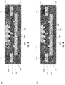
- Figures 6A and 6B each show a top-down plan view and corresponding cross-sectional view during different stages of the cavity sealing method.
- the cavity is sealed prior to application of the chip-package encapsulation.
- Figure 6A shows a first chip 500 coupled to the first side 502 of a carrier 504 by a coupling structure 506.
- the first chip 500 is a SAW filter chip and the resulting package forms an RF module.
- the SAW filter chip 500 may have a flip-chip configuration and a cavity 508 between the first chip 500 and the carrier 504 is sealed by a 2-part gluing process.
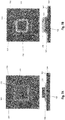
- Figure 6A shows the first part of the gluing process, in which a ring of glue 510 is dispensed on the carrier 504 around the perimeter of the first chip 500.
- the ring of glue 510 has a thixotropy in a range between 3.5 and 4.0.
- Figure 6B shows the second part of the gluing process, in which a glob of glue 512 is dispensed on the first chip 500 within the perimeter defined by the ring of glue 510.
- a glob of glue 512 is dispensed on the first chip 500 within the perimeter defined by the ring of glue 510.
- the glob of glue 512 has a thixotropy in a range between 3.5 and 4.0.
- the ring of glue 510 may have a thixotropy of about 3.5 and the glob of glue 512 may have a thixotropy of about 4.0.
- the ring of glue 510 together with the glob of glue 512 form a glue-based sealing structure which seals the air cavity 508, preventing mold compound from seeping under the first chip 500 during a subsequent mold process such as film-assisted molding, transfer molding, injection molding, etc.
- the glues 510, 512 used to seal the cavity 508 each comprise a silicone material such as silicone die attach material KJR 9602 series sold by Shin-Etsu MicroSi.
- the resulting glue-on-glue cavity sealing structure allows for reduced package size, and the use of epoxy-based glues provides better adhesion as compared to Si and metal lids.
- the carrier 504 may have various metal pads 514 and conductive vias 516, to facilitate electrical connections to the package and first chip 500.
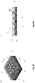
- Figure 6C shows an image of an actual exemplary package 600 having a cavity sealed 508 formed by the method shown in Figures 6A and 6B .
- the glues 510, 512 together form a glue-based sealing structure which seals the air cavity 508, preventing mold compound 602 from seeping under the first chip 500 during a subsequent mold process such as film-assisted molding, transfer molding, injection molding, etc.
- the glue-based sealing structure formed by the glues 510, 512 laterally surrounds the first chip 500 and, together with the chip 500 and the carrier 504, defines the cavity 508 between the carrier 504 and the chip 500.
- Figures 7A and 7B illustrate another embodiment of sealing a cavity of a chip-package.
- Figures 7A and 7B each show a top-down plan view and corresponding cross-sectional view during different stages of the cavity sealing method.
- the embodiment shown in Figures 7A and 7B is similar to the embodiment illustrated in Figures 6A and 6B .
- a glue writing/printing process is used instead of a glob-top process.
- Figure 7A shows a ring of glue 510 dispensed on the carrier 504 around the perimeter of the first chip 500.
- Figure 7B shows the second part of the gluing process, in which a second ring of glue 700 is dispensed into the gap 702 between the first chip 500 and the first ring of glue 510.
- the second ring of glue 700 is dispensed by a standard writing/printing process instead of a glob top process.
- the second ring of glue 700 may be printed by either screen or stencil.
- the glue-based cavity sealing structures described herein may be subject to pressure that build-ups during the glue curing process. If unmitigated, the pressure may cause the glue-based sealing structure to bulge and possibly rupture, providing a path for encapsulation material to subsequently enter.
- the cavity may be partly or completely filled with the encapsulation material if the glue-based cavity sealing structure ruptures, rendering the chip adjacent the filled cavity ineffective for its intended use.
- a MEMS-based pressure sensor or SAW filter would function poorly if at all if a mold compound entered the cavity and solidified against the sensitive area of the chip.
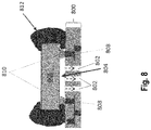
- Figure 8 illustrates a cross-sectional view of an embodiment of a carrier 800 which has one or more vent holes 802 for providing a passage to a cavity 804 formed between the carrier 800 and a chip 806 coupled to electrically conductive regions 808 of the carrier 800 by a coupling structure 810.
- a glue-based cavity sealing structure 812 e.g. of the kind previously described herein in connection with Figures 6A-6B or 7A-7B , seals the cavity 804 between the carrier 800 and the chip 806.
- the vent hole(s) 802 remain unplugged during the glue curing process, so that pressure which builds-up in the cavity 804 during glue curing can escape through the vent hole(s) 802.
- the escaping gas is illustrated as downward dashed arrows in Figure 8 .
- the passage formed by the vent hole(s) 802 may be sealed at the exit side after completion of the glue curing, e.g., to prevent encapsulation material from subsequently entering the cavity 804 through the vent hole(s) 802.
- a material (not shown) may at least partly fill the vent hole(s) 802 to close off the passage.
- the material at least partly filling the vent hole(s) 802 may comprises solder, a Cu pillar, a SnAg bump, glue and/or epoxy, etc.
- the passage formed by the vent hole(s) 802 may be designed to be resistant towards the air path sealing material, for example, with a partially or fully coated finish, and not limited to a copper finish with solder deposition to cover, gold finish for chip sealing, glue material, etc.
- Figures 9A through 9C illustrate an embodiment of forming vent holes in a carrier.
- Figure 9A shows a top plan view of the carrier 900 after vent holes 902 are formed in the carrier 900, and before a chip 904 is coupled to the carrier 900 by a coupling structure 906.
- the carrier 900 may include plated through-holes 908 for providing electrical connections between both sides of the carrier 900.
- the carrier 900 may also include metal pads 910 connected by metal traces 912 to the plated through-holes 908.
- the carrier 900 further includes vent holes 902.
- the vent holes 902 may be formed in the same way as the through-holes 908, e.g., by laser drilling, mechanical drilling using a drill bit, etc.
- the vent holes 902 may or may not be plated.
- Figure 9B shows the carrier 900 after the chip 904 is coupled to the carrier 900 by the coupling structure 906.
- the coupling structure 906 may include Cu pillars, filled vias, solder, etc. and provides a distance (d1) between the first chip 904 and the carrier 900, as previously described herein.
- the coupling structure 906 is connected to the metal pads 910 of the carrier 900.
- Figure 9C is a cross-sectional view along the line labelled C-C' in Figure 9B .
- the vent holes 902 remain unplugged until after the cavity 914 between the carrier 900 and the chip 904 is sealed, e.g., using a glue-based cavity sealing structure 916 of the kind previously described herein in connection with Figures 6A-6B or 7A-7B .
- the glue-based sealing structure 916 at least laterally surrounds the chip 904, and together with the chip 904 and the carrier 900, defines the cavity 914 between the carrier 900 and the chip 904. Pressure which builds-up in the cavity 914 during the glue curing process escapes through the vent holes 902.
- the vent holes 902 may be filled/sealed after completion of the glue curing, e.g., as previously described herein.
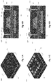
- Figure 10A illustrates a top-down plan view of a plurality of chips 1000 coupled to a PCB-based carrier 1002.
- a glue-based sealing structure 1004 is provided for each chip 1000, to seal the cavity between the carrier 1002 and the respective chips 1000.
- the carrier 1002 shown in Figure 10A does not include vent holes for releasing pressure during the glue curing process.
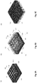
- Bulges 1006 in the glue-based sealing structures 1004 are plainly evident in Figure 10A .
- the glue curing process was performed at 150C for 2 hours in this example, and the bulging began to occur at 35C and continued even after the curing conditions were removed.
- Figure 10B illustrates a top-down plan view of the same PCB-based carrier 1002 as shown in Figure 10A , but vent holes which are out of view in Figure 10B below the chips 1000 are formed in the carrier 1002 as previously described herein.
- the vent holes provide a passage to the respective cavities under the chips 1000, allowing pressure which builds-up during the glue curing process to escape.
- the glue-based sealing structures 1004 in Figure 10B did experience bulging during the same curing conditions as in Figure 10A .
- the vent holes may be filled/sealed after the glue curing process, as previously described herein.
- Figures 11A through 11D illustrate another embodiment of a chip-package 1100 having an arrangement of stacked chips 408, 412.
- the embodiment shown in Figures 11A through 11D is similar to the embodiment illustrated in Figures 5A through 5G .
- the electrically conductive material 420 fills the vias 418 in the periphery of the upper portion 116a of the encapsulation 116 to form wire-like conductors 1102.
- a notch or recess 1104 may be formed in the outer side of the encapsulation material 416 at which the wire-like conductors 1102 terminate.
- a solder bump 1106 may be formed in each notch/recess 1104 for electrically contacting the wire-like conductors 1102 at a first end of the vias 418.
- FIG. 11A shows the chip-package 1100 after the notches/recesses 1104 are formed in the encapsulation 416, but before via plating and before solder bump formation.
- Figure 11B shows a corresponding cross-sectional view along the line labeled D-D' in Figure 11A , but after via plating.
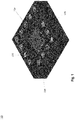
- Figure 11C shows the chip-package 1100 after the solder bumps 1106 are formed in the notches/recesses 1104 in the encapsulation 416, and Figure 11D shows a corresponding cross-sectional view along the line labeled D-D' in Figure 11C .
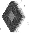
- Figure 12 illustrates a side perspective view of another embodiment of a chip-package 1200 having an arrangement of stacked chips.
- the embodiment shown in Figure 12 is similar to the embodiment illustrated in Figures 11A through 11D .
- the chip 408 adjacent the sealed cavity has an exposed surface 1202, which can be readily realized during the encapsulation process.
- Figure 12 shows certain internal details of the package 1200 in view in the lower part of the package 1200.
Landscapes
- Engineering & Computer Science (AREA)
- Microelectronics & Electronic Packaging (AREA)
- Manufacturing & Machinery (AREA)
- Computer Hardware Design (AREA)
- Chemical & Material Sciences (AREA)
- Analytical Chemistry (AREA)
- Structures Or Materials For Encapsulating Or Coating Semiconductor Devices Or Solid State Devices (AREA)
- Micromachines (AREA)
- Physics & Mathematics (AREA)
- Geometry (AREA)
Abstract
Description
- Two or more semiconductor chips (dies) are often integrated in the same package, e.g., in the case of a power transistor die and a driver die, a sensor die and a controller die, etc. Some conventional multi-chip packaging solutions use multiple PCBs (printed circuit boards) to stack chips, which increases overall packaging cost. Chip stacking also has increased manufacturing complexity. For example, a high precision wire bond technique may be needed which is costly. Also, the likelihood of chip damage increases due to the complex manufacturing process. Other conventional solutions use chip embedding. Chip embedding also is complex, and involves a serial manufacturing process. Chip embedding offers no flexibility in chip variation once a chip is fixed in place. Chip embedding may suffer from artificially high yield loss since a good chip will be lost if a faulty package cannot be reworked.
- Some package solutions require a cavity, e.g., in the case of a MEMS (microelectromechanical systems) sensor solution. The membrane of a MEMS sensor should not be contacted by the encapsulation material for the package. A metal lid may be used to cover and protect the MEMS sensor, but increases package height. A Si lid may instead be attached by silicone to cover and protect the MEMS sensor, but increases package cost. Silicone glue may instead be used to cover and protect the MEMS sensor, but may bleed which is hard to control.
- Thus, there is a need for improved chip-packages.
- According to an embodiment of a chip-package, the chip-package comprises: a carrier having a first side and a second side opposing the first side; a first chip coupled to the first side of the carrier; a second chip coupled to the second side of the carrier; an encapsulation with a first portion, which at least partially encloses the first chip on the first side of the carrier, and a second portion, which at least partially encloses the second chip on the second side of the carrier; a via extending through the first portion of the encapsulation, the carrier and the second portion of the encapsulation; and an electrically conductive material at least partly covering a sidewall of the via in the first portion or the second portion of the encapsulation, to electrically contact the carrier at either the first side or the second side.
- An upper half or a lower half of the via may be plated by the electrically conductive material, and the other half of the via may be devoid of the electrically conductive material.
- Separately or in combination, an upper half and a lower half of the via may each be plated by the electrically conductive material, one of the plated halves of the via electrically may contact the carrier at one of the sides of the carrier, and the other plated half of the via may provide a thermal conduction path to the other side of the carrier.
- Separately or in combination, the first chip and the second chip may be vertically aligned.
- Separately or in combination, the chip-package may further comprise a metallization layer located on the first portion or the second portion of the encapsulation, wherein the metallization layer comprises a metal pad and a metal trace which connects the metal pad to the electrically conductive material at a first end of the via, and wherein the electrically conductive material electrically contacts the carrier at a second end of the via opposite the first end.
- Separately or in combination, a ratio of a depth of the via to a width of the via may be greater than 1:1.
- Separately or in combination, the electrically conductive material may fill the via in the first portion or the second portion of the encapsulation.
- Separately or in combination, the chip-package may further comprise a solder bump electrically contacting the electrically conductive material at a first end of the via, wherein the electrically conductive material electrically contacts the carrier at a second end of the via opposite the first end.
- Separately or in combination, the chip-package may further comprise a cavity between the first chip and the carrier, or between the second chip and the carrier.
- Separately or in combination, the chip-package may further comprise a material sealing the cavity around a perimeter of a recess formed in the encapsulation and in which the first chip or the second chip is disposed.
- Separately or in combination, the material may be a polymer clay, an insulative rigid foam or a gel.
- Separately or in combination, the first chip or the second chip may be a MEMS chip, and the cavity may abut the MEMS chip.
- Separately or in combination, the chip-package may further comprise a glue-based sealing structure sealing the cavity.
- Separately or in combination, the glue-based sealing structure may comprise a first glue laterally surrounding the first chip or the second chip and a second glue covering the chip laterally surrounded by the first glue.
- Separately or in combination, the glue-based sealing structure may comprise a first glue laterally surrounding the first chip or the second chip and a second glue filling a gap between the first glue and the chip laterally surrounded by the first glue.
- Separately or in combination, the chip-package further comprises one or more vent holes formed in the carrier and providing a passage to the cavity.
- Separately or in combination, the chip-package may further comprise a material at least partly filling the one or more vent holes to close off the passage.
- Separately or in combination, the material at least partly filling the one or more vent holes may comprise solder, a Cu pillar, a SnAg bump, glue and/or epoxy.
- According to an embodiment of a chip-package, the chip-package comprises: a carrier having a first side and a second side opposing the first side; a first chip coupled to the first side of the carrier; an encapsulation which at least partially encloses the first chip on the first side of the carrier; a cavity between the first chip and the carrier; a glue laterally surrounding the first chip and partly defining the cavity; and one or more vent holes formed in the carrier and providing a passage to the cavity. The chip-package may further comprise a material at least partly filling the one or more vent holes to close off the passage. Separately or in combination, the material at least partly filling the one or more vent holes may comprise solder, a Cu pillar, a SnAg bump, glue and/or epoxy.
- According to an embodiment of a chip-package, the chip-package comprises: a carrier with a first side; a first chip coupled to the first side of the carrier by a coupling structure, wherein the coupling structure provides a distance between the first chip and the carrier; and an encapsulation on the first side of the carrier, wherein the encapsulation is at least partially laterally spaced apart from the first chip as to form a gap between the first chip and the encapsulation, wherein the gap extends to the first side of the carrier. The gap may comprise an air gap. Separately or in combination, the chip-package may further comprise a material in the gap between the first chip and the encapsulation, wherein a cavity is formed by the material in the gap, the carrier and the chip.
- Those skilled in the art will recognize additional features and advantages upon reading the following detailed description, and upon viewing the accompanying drawings.
- The elements of the drawings are not necessarily to scale relative to each other. Like reference numerals designate corresponding similar parts. The features of the various illustrated embodiments can be combined unless they exclude each other. Embodiments are depicted in the drawings and are detailed in the description which follows.
-
Figure 1 illustrates a side perspective view of an embodiment of a chip-package having an arrangement of stacked chips. -
Figures 2A and 2B illustrate the chip-package 100 at different stages of manufacturing. -
Figure 3 illustrates a cross-sectional view of the chip-package ofFigure 1 with a material provided in a lateral gap between a chip and an encapsulation. -
Figure 4 illustrates a cross-sectional view of the chip-package ofFigure 1 with a material provided in the lateral gap between the chip and the encapsulation, according to another embodiment. -
Figures 5A through 5G illustrate different views of another embodiment of a chip-package having an arrangement of stacked chips. -
Figures 6A and 6B illustrate an embodiment of sealing a cavity of a chip-package. -
Figure 6C illustrates an image of an actual exemplary package having a cavity sealed formed by the method shown inFigures 6A and 6B . -
Figures 7A and 7B illustrate another embodiment of sealing a cavity of a chip-package. -
Figure 8 illustrates a cross-sectional view of an embodiment of a chip-package carrier having one or more vent holes. -
Figures 9A through 9C illustrate an embodiment of forming vent holes in a chip-package carrier. -
Figure 10A illustrates a top-down plan view of a PCB-based carrier without vent holes in the chip-package carriers, andFigure 10B illustrates a top-down plan view of the same PCB-based carrier with vent holes in the carriers. -
Figures 11A through 11D illustrate different views of another embodiment of a chip-package having an arrangement of stacked chips. -
Figure 12 illustrates a side perspective view of another embodiment of a chip-package having an arrangement of stacked chips. - The embodiments described herein provide chip-packages and corresponding methods of manufacture. In some embodiments, the chip-package has one or more vias which extend through entire thickness of the package. One half of the via(s) may be used for electrical connections to a chip included in the package. The other half of the via(s) may provide a thermal conduction path at the opposite side of the package. This half of the via(s) may or may not also provide electrical connections, e.g., to the same or different chip included in the package. In some embodiments, the chip-package may have a cavity, e.g., in the case of a MEMS sensor or SAW (surface acoustic wave) filter application. The cavity may be partly defined by a cured solid material, cured glue, etc. In the case of glue being used to partly define the cavity, one or more vent holes may be formed in the carrier for the MEMS sensor to relieve pressure which builds-up in the cavity during curing of the glue. In some embodiments, the chip carrier included in the chip-package may be a lead frame instead of a PCB (printed circuit board) and the package encapsulation may be at least partially laterally spaced apart from the chip as to form a gap between the chip and the encapsulation. Still other embodiments are described. It is to be understood that the features of the various embodiments described herein may be combined with each other, unless specifically noted otherwise. Various examples are provided at the end of this section, as illustrative combinations of the embodiments described herein.
-
Figure 1 illustrates a side perspective view of an embodiment of a chip-package 100.Figures 2A and 2B illustrate the chip-package 100 at different stages of manufacturing. - The chip-
package 100 includes acarrier 102 with afirst side 104. In one embodiment, thecarrier 102 is a lead frame. Afirst chip 106 is coupled to thefirst side 104 of thecarrier 102 by acoupling structure 108. Thecoupling structure 108 may include Cu pillars, filled vias, solder, etc. Thecoupling structure 108 provides a distance (d1) between thefirst chip 106 and thecarrier 102. The chip-package 100 may include asecond chip 110 coupled to the opposingsecond side 112 of thecarrier 102 by acoupling structure 114 which may include Cu pillars, filled vias, solder, etc. and provides a distance (d2) between thesecond chip 110 and thecarrier 102. In one example, the chip-package 100 forms an RF module, thefirst chip 106 is a MEMS-based tunable filter and thesecond chip 110 is an RF chip. - An
encapsulation 116, such as a mold compound, is provided on the first andsecond sides carrier 102. Theencapsulation 116 is at least partially laterally spaced apart from thefirst chip 106 as to form alateral gap 118, e.g. an air gap, between thefirst chip 106 and theencapsulation 116. Thelateral gap 118 may extend to thefirst side 104 of thecarrier 102. Thelateral gap 118 allows for proper operation of asensitive area 120 such as a membrane or similar structure in the case of a MEMS-based tunable filter, MEMS sensor, etc., by preventing theencapsulation 116 from impinging upon thesensitive area 120 of thefirst chip 106. -
Figure 2A shows the chip-package 100 after thesecond chip 110 is coupled to thesecond side 112 of thecarrier 102 and theencapsulation 116 is formed. Thesecond chip 110 is embedded in theencapsulation 116 and coupled to thesecond side 112 of thecarrier 102 by acoupling structure 114. At the side of the encapsulation opposite thesecond chip 110, vias 122 formed e.g. by laser drilling to exposecontact areas 124 of thecarrier 102, e.g., leads in the case of a lead frame-based carrier or metal pads in the case of a PCB-based carrier. Thevias 122 may be plated or filled, to form electrical connections to thecoupling structure 114. Acavity 126 is formed in the side of theencapsulation 116 opposite thesecond chip 110. For example, in the case of a mold compound as theencapsulation 116, thecavity 126 may be molded into theencapsulation 116 during a standard molding process such as film-assisted molding, transfer molding, injection molding, etc. to form a pre-molded frame which includes thesecond chip 110. Electrical connections between thesecond chip 110 and thecarrier 102 are formed prior to molding, e.g., via thesecond coupling structure 114. -
Figure 2B shows the chip-package after thefirst chip 106 is positioned in thecavity 126 and coupled to thecarrier 102 by the correspondingcoupling structure 108. Thecavity 126 is larger than thefirst chip 106 so that theencapsulation 116 is at least partially laterally spaced apart from thefirst chip 106, thereby forming alateral gap 118 such as an air gap between thefirst chip 106 and theencapsulation 116.Bonds pads 128 of thecarrier 102 to which thefirst chip 106 is to be coupled are exposed in thecavity 126 prior to coupling of thefirst chip 106. In one embodiment, thefirst chip 106 has a flip-chip configuration and thecoupling structure 108 has Cu pillars or solder bumps which couple thefirst chip 106 to the exposedbond pads 128 of thecarrier 102. Laser direct imaging may be used to expose thebond pads 128 and form thevias 122 in the perimeter of theencapsulation 116. A typical die bond process may be used to land thefirst chip 106 into the pre-molded frame. -
Figure 3 shows the chip-package 100 ofFigure 1 after amaterial 200 is provided in thelateral gap 118 between thefirst chip 106 and theencapsulation 116. Thematerial 200 fills the perimeter of thelateral gap 118, thereby forming acavity 202 defined by thematerial 200 in thegap 118, thecarrier 102 and thefirst chip 106. Thecavity 202 may be sealed, depending on the contiguousness and porosity of the material 200 filling the perimeter of thelateral gap 118. In one embodiment, a semisolid material such as polymer clay, high-density insulative rigid foam (PE foam), gel, etc. is dispensed along the perimeter of thelateral gap 118 to fill the empty lateral space between thefirst chip 106 and theencapsulation 116 but not cover thesensitive area 120 of thefirst chip 106. The semisolid material may solidify after curing at elevated temperature. For example, polymer clay is essentially PVC (polyvinyl chloride) which is plastic, but until cured, is a very malleable plastic. Polymer clay can be shaped and reshaped a multitude of times without deterioration. Once cured, polymer clay is hard and durable. -
Figure 4 shows another embodiment of the chip-package 100 ofFigure 1 after amaterial 300 is provided in thelateral gap 118 between thefirst chip 106 and theencapsulation 116. As described above in connection withFigure 3 , a semisolid material such as polymer clay, high-density insulative rigid foam (PE foam), gel, etc. may be dispensed along the perimeter of thelateral gap 118 to fill the empty space but not cover thesensitive area 120 of thefirst chip 106, and then solidified by curing at elevated temperature. - The shape of the material 200/300 post-curing may differ depending on the type of material used, the manner in which the
material 200/300 is dispensed and shaped, etc., as shown inFigures 3 and 4 . For example, the top surface of the material 200 inFigure 3 has a convex shape, the top surface of the material 300 inFigure 4 has a concave shape, or thematerial 200/300 may have yet another shape (e.g., flat, undulating, etc.). The material 200 inFigure 3 laterally extends to the outermost part of thecoupling structure 108 for thefirst chip 106. The material 300 inFigure 4 terminates laterally before reaching the outermost part of thecoupling structure 108, so that there is alateral gap 302 between the material 300 and the outermost part of thecoupling structure 108. -
Figures 5A through 5G illustrate another embodiment of a chip-package 400 having an arrangement of stacked chips.Figure 5A shows a top-side perspective view of the chip-package 400,Figure 5B shows the same view asFigure 5A but with certain internal details of thepackage 400 in view, andFigure 5C shows a bottom-side perspective view of the chip-package 400.Figure 5D shows a cross-sectional view of the chip-package 400 along the line labelled A-A' inFigure 5B , andFigure 5E shows a corresponding side perspective view of the chip-package 500 of the cross-section shown inFigure 5D .Figure 5F shows a cross-sectional perspective view of the chip-package 500 taken along the line labelled B-B' inFigure 5B , andFigure 5G shows a corresponding side view of the chip-package 500 along the cross-sectioned plane illustrated inFigure 5F . - According to the embodiment illustrated in
Figures 5A through 5G , the chip-package 400 includes acarrier 402, such as a PCB, having afirst side 404 and asecond side 406 opposing thefirst side 404. Afirst chip 408 is coupled to thefirst side 404 of thecarrier 402 by acoupling structure 410. Thecoupling structure 410 may include Cu pillars, filled vias, solder, etc. Thecoupling structure 410 provides a distance (d1) between thefirst chip 408 and thecarrier 402. Asecond chip 412 is coupled to thesecond side 406 of thecarrier 402 by acoupling structure 414 which may include Cu pillars, filled vias, solder, etc. and provides a distance (d2) between thesecond chip 412 and thecarrier 402. Thechips package 400 and yielding a leadless package on both sides with surface I/O and having a small footprint. For example, the distance between thechips package 400 can be reduced by 40%. - The chip-
package 400 also includes anencapsulation 416 with afirst portion 416a and asecond portion 416b. Thefirst portion 416a of theencapsulation 416 at least partially encloses thefirst chip 408 at thefirst side 404 of thecarrier 402, and thesecond portion 416b of theencapsulation 416 at least partially encloses thesecond chip 412 at thesecond side 406 of thecarrier 402. One ormore vias 418 extend through thefirst portion 416a of theencapsulation 416, thecarrier 402 and thesecond portion 416b of theencapsulation 416. An electricallyconductive material 420 at least partly covers a sidewall of some or all of thevias 420 in thefirst portion 416a or thesecond portion 416b of theencapsulation 416, to electrically contactmetal contact areas 403 of thecarrier 402 at either thefirst side 404 or thesecond side 406. - In one embodiment, the electrically
conductive material 420 is formed by plating the upper half or the lower half of thevias 418. The other half of thevias 418 may be devoid of the electricallyconductive material 420. For example, the upper or lower half of thevias 418 may be precoated so that a plating solution does not adhere / plate this part of thevias 418. A mold compound is mixed with metal powder and insulation material to enable plating of the other half of thevias 418. A laser may be used to remove / burn-off the insulation material that insulates the metal powder to expose the metal, allowing the plating material to plate the metal. The coating remaining on the other part of the sidewall ensures the plating solution effectively passes through thevias 418. - In another embodiment, both the upper half and the lower half of the
vias 418 are plated by the electricallyconductive material 420. The upper or lower plated half of one or more of thevias 418 electrically contactsmetal contact areas 403 of thecarrier 402 at one of thesides carrier 402, and the other plated half provides a thermal conduction path to theother side carrier 402.Figures 5D through 5G show only the upper half of thevias 418 plated by the electricallyconductive material 420, however, the lower half may instead be plated, or both halves may be coated, e.g., omitting the pre-coating step described above. - Regardless of whether only one half or both halves of the
vias 418 are plated with the electricallyconductive material 420, a targeted laser may be used to form relativelysmall vias 418. The ratio of the depth / height (H) of thevias 418 to the width (W) of thevias 418 may be greater than 1:1, e.g., greater than 10:1. For example, the via height (H) may be 1mm and the width (W) may be 0.1mm.Other vias 422 may be formed which extend to thecarrier 402 through either thefirst portion 416a or thesecond portion 416b of the encapsulation, but not through bothportions vias 422 may be coated with the same or different electricallyconductive material 420, and may electrically contactmetal contact areas 403 of thecarrier 402 at oneside 404/406. - A
metallization layer 424 may be located on thefirst portion 416a or thesecond portion 416b of theencapsulation 416. Eachmetallization layer 424 may includemetal pads 426 and respective metal traces 428. Themetal pads 426 provide I/O interconnection points for thepackage 400. The metal traces 428 connect thecorresponding metal pads 426 to the electricallyconductive material 420 at a first end of a via 418/422, and the electricallyconductive material 420 electrically contacts ametal contact area 403 of thecarrier 402 at a second end of thevia 418/422 opposite the first end. - The chip-
package 400 may further include acavity 430 between thefirst chip 408 and thecarrier 402, or between thesecond chip 412 and thecarrier 402. In one embodiment, the chip-package 400 is a QFP (quad flat package) which forms an RF module, thefirst chip 408 is a MEMS-based tunable filter and thesecond chip 412 is an RF chip. According to this embodiment, thecavity 430 is provided between the MEMS-based tunable filter and thecarrier 402. Thecavity 430 may be sealed by amaterial 432 disposed in thecavity 430 and which surrounds the periphery of thefirst chip 408. -
Figures 6A and 6B illustrate an embodiment of sealing a cavity of a chip-package.Figures 6A and 6B each show a top-down plan view and corresponding cross-sectional view during different stages of the cavity sealing method. According to the embodiment illustrated inFigures 6A and 6B , the cavity is sealed prior to application of the chip-package encapsulation.Figure 6A shows afirst chip 500 coupled to thefirst side 502 of acarrier 504 by acoupling structure 506. In one embodiment, thefirst chip 500 is a SAW filter chip and the resulting package forms an RF module. TheSAW filter chip 500 may have a flip-chip configuration and acavity 508 between thefirst chip 500 and thecarrier 504 is sealed by a 2-part gluing process. -
Figure 6A shows the first part of the gluing process, in which a ring ofglue 510 is dispensed on thecarrier 504 around the perimeter of thefirst chip 500. In one embodiment, the ring ofglue 510 has a thixotropy in a range between 3.5 and 4.0. -
Figure 6B shows the second part of the gluing process, in which a glob ofglue 512 is dispensed on thefirst chip 500 within the perimeter defined by the ring ofglue 510. Such a process is commonly referred to as glob-top. In one embodiment, the glob ofglue 512 has a thixotropy in a range between 3.5 and 4.0. For example, the ring ofglue 510 may have a thixotropy of about 3.5 and the glob ofglue 512 may have a thixotropy of about 4.0. The ring ofglue 510 together with the glob ofglue 512 form a glue-based sealing structure which seals theair cavity 508, preventing mold compound from seeping under thefirst chip 500 during a subsequent mold process such as film-assisted molding, transfer molding, injection molding, etc. In one embodiment, theglues cavity 508 each comprise a silicone material such as silicone die attach material KJR 9602 series sold by Shin-Etsu MicroSi. The resulting glue-on-glue cavity sealing structure allows for reduced package size, and the use of epoxy-based glues provides better adhesion as compared to Si and metal lids. Thecarrier 504 may havevarious metal pads 514 andconductive vias 516, to facilitate electrical connections to the package andfirst chip 500. -
Figure 6C shows an image of an actualexemplary package 600 having a cavity sealed 508 formed by the method shown inFigures 6A and 6B . Theglues air cavity 508, preventingmold compound 602 from seeping under thefirst chip 500 during a subsequent mold process such as film-assisted molding, transfer molding, injection molding, etc. The glue-based sealing structure formed by theglues first chip 500 and, together with thechip 500 and thecarrier 504, defines thecavity 508 between thecarrier 504 and thechip 500. -
Figures 7A and 7B illustrate another embodiment of sealing a cavity of a chip-package.Figures 7A and 7B each show a top-down plan view and corresponding cross-sectional view during different stages of the cavity sealing method. The embodiment shown inFigures 7A and 7B is similar to the embodiment illustrated inFigures 6A and 6B . Different, however, a glue writing/printing process is used instead of a glob-top process. Similar toFigure 6A ,Figure 7A shows a ring ofglue 510 dispensed on thecarrier 504 around the perimeter of thefirst chip 500.Figure 7B shows the second part of the gluing process, in which a second ring ofglue 700 is dispensed into thegap 702 between thefirst chip 500 and the first ring ofglue 510. Different than the embodiment shown inFigure 6B , the second ring ofglue 700 is dispensed by a standard writing/printing process instead of a glob top process. For example, the second ring ofglue 700 may be printed by either screen or stencil. - The glue-based cavity sealing structures described herein may be subject to pressure that build-ups during the glue curing process. If unmitigated, the pressure may cause the glue-based sealing structure to bulge and possibly rupture, providing a path for encapsulation material to subsequently enter. The cavity may be partly or completely filled with the encapsulation material if the glue-based cavity sealing structure ruptures, rendering the chip adjacent the filled cavity ineffective for its intended use. For example, a MEMS-based pressure sensor or SAW filter would function poorly if at all if a mold compound entered the cavity and solidified against the sensitive area of the chip.
-
Figure 8 illustrates a cross-sectional view of an embodiment of acarrier 800 which has one or more vent holes 802 for providing a passage to acavity 804 formed between thecarrier 800 and achip 806 coupled to electricallyconductive regions 808 of thecarrier 800 by acoupling structure 810. A glue-basedcavity sealing structure 812, e.g. of the kind previously described herein in connection withFigures 6A-6B or7A-7B , seals thecavity 804 between thecarrier 800 and thechip 806. The vent hole(s) 802 remain unplugged during the glue curing process, so that pressure which builds-up in thecavity 804 during glue curing can escape through the vent hole(s) 802. The escaping gas is illustrated as downward dashed arrows inFigure 8 . - The passage formed by the vent hole(s) 802 may be sealed at the exit side after completion of the glue curing, e.g., to prevent encapsulation material from subsequently entering the
cavity 804 through the vent hole(s) 802. For example, a material (not shown) may at least partly fill the vent hole(s) 802 to close off the passage. The material at least partly filling the vent hole(s) 802 may comprises solder, a Cu pillar, a SnAg bump, glue and/or epoxy, etc. The passage formed by the vent hole(s) 802 may be designed to be resistant towards the air path sealing material, for example, with a partially or fully coated finish, and not limited to a copper finish with solder deposition to cover, gold finish for chip sealing, glue material, etc. -
Figures 9A through 9C illustrate an embodiment of forming vent holes in a carrier.Figure 9A shows a top plan view of thecarrier 900 after vent holes 902 are formed in thecarrier 900, and before achip 904 is coupled to thecarrier 900 by acoupling structure 906. Thecarrier 900 may include plated through-holes 908 for providing electrical connections between both sides of thecarrier 900. Thecarrier 900 may also includemetal pads 910 connected bymetal traces 912 to the plated through-holes 908. Thecarrier 900 further includes vent holes 902. The vent holes 902 may be formed in the same way as the through-holes 908, e.g., by laser drilling, mechanical drilling using a drill bit, etc. The vent holes 902 may or may not be plated.Figure 9B shows thecarrier 900 after thechip 904 is coupled to thecarrier 900 by thecoupling structure 906. Thecoupling structure 906 may include Cu pillars, filled vias, solder, etc. and provides a distance (d1) between thefirst chip 904 and thecarrier 900, as previously described herein. Thecoupling structure 906 is connected to themetal pads 910 of thecarrier 900.Figure 9C is a cross-sectional view along the line labelled C-C' inFigure 9B . As shown inFigure 9C , the vent holes 902 remain unplugged until after thecavity 914 between thecarrier 900 and thechip 904 is sealed, e.g., using a glue-basedcavity sealing structure 916 of the kind previously described herein in connection withFigures 6A-6B or7A-7B . The glue-basedsealing structure 916 at least laterally surrounds thechip 904, and together with thechip 904 and thecarrier 900, defines thecavity 914 between thecarrier 900 and thechip 904. Pressure which builds-up in thecavity 914 during the glue curing process escapes through the vent holes 902. The vent holes 902 may be filled/sealed after completion of the glue curing, e.g., as previously described herein. -
Figure 10A illustrates a top-down plan view of a plurality ofchips 1000 coupled to a PCB-basedcarrier 1002. A glue-basedsealing structure 1004 is provided for eachchip 1000, to seal the cavity between thecarrier 1002 and therespective chips 1000. Thecarrier 1002 shown inFigure 10A does not include vent holes for releasing pressure during the glue curing process.Bulges 1006 in the glue-basedsealing structures 1004 are plainly evident inFigure 10A . The glue curing process was performed at 150C for 2 hours in this example, and the bulging began to occur at 35C and continued even after the curing conditions were removed. -
Figure 10B illustrates a top-down plan view of the same PCB-basedcarrier 1002 as shown inFigure 10A , but vent holes which are out of view inFigure 10B below thechips 1000 are formed in thecarrier 1002 as previously described herein. The vent holes provide a passage to the respective cavities under thechips 1000, allowing pressure which builds-up during the glue curing process to escape. The glue-basedsealing structures 1004 inFigure 10B did experience bulging during the same curing conditions as inFigure 10A . The vent holes may be filled/sealed after the glue curing process, as previously described herein. -
Figures 11A through 11D illustrate another embodiment of a chip-package 1100 having an arrangement ofstacked chips Figures 11A through 11D is similar to the embodiment illustrated inFigures 5A through 5G . Different, however, the electricallyconductive material 420 fills thevias 418 in the periphery of the upper portion 116a of theencapsulation 116 to form wire-like conductors 1102. A notch orrecess 1104 may be formed in the outer side of theencapsulation material 416 at which the wire-like conductors 1102 terminate. Asolder bump 1106 may be formed in each notch/recess 1104 for electrically contacting the wire-like conductors 1102 at a first end of thevias 418. The wire-like conductors 1102 contact thecarrier 402 at a second end of thevias 418 opposite the first end.Figure 11A shows the chip-package 1100 after the notches/recesses 1104 are formed in theencapsulation 416, but before via plating and before solder bump formation.Figure 11B shows a corresponding cross-sectional view along the line labeled D-D' inFigure 11A , but after via plating.Figure 11C shows the chip-package 1100 after the solder bumps 1106 are formed in the notches/recesses 1104 in theencapsulation 416, andFigure 11D shows a corresponding cross-sectional view along the line labeled D-D' inFigure 11C . -
Figure 12 illustrates a side perspective view of another embodiment of a chip-package 1200 having an arrangement of stacked chips. The embodiment shown inFigure 12 is similar to the embodiment illustrated inFigures 11A through 11D . Different, however, thechip 408 adjacent the sealed cavity has an exposedsurface 1202, which can be readily realized during the encapsulation process.Figure 12 shows certain internal details of thepackage 1200 in view in the lower part of thepackage 1200. - Various chip-package embodiments have been illustrated and described. The following examples are also provided.
- Example 1: a chip-package comprises a carrier having a first side and a second side opposing the first side, a first chip coupled to the first side of the carrier, a second chip coupled to the second side of the carrier, an encapsulation with a first portion, which at least partially encloses the first chip on the first side of the carrier, and a second portion, which at least partially encloses the second chip on the second side of the carrier, at least one via, wherein the via extends through the first portion of the encapsulation, the carrier and the second portion of the encapsulation, and an electrically conductive material at least partially filling the at least one via to electrically contact the carrier. A corresponding method of forming a chip-package comprises: providing a carrier with a first side and a second side opposing the first side; coupling a first chip to the first side of the carrier; coupling a second chip to the second side of the carrier; at least partially encapsulating the first chip on the first side of the carrier with a first portion of an encapsulation and at least partially encapsulating the second chip on the second side of the carrier with a second portion of the encapsulation; forming at least one via, wherein the via extends through the first portion of the encapsulation, the carrier and the second portion of the encapsulation; and at least partially filling an electrically conductive material into the at least one via to electrically contact the carrier.
- Example 2: the chip-package / method of example 1 wherein the carrier comprises at least one metallization layer and the first chip and the second chip are electrically coupled to the metallization layer.
- Example 3: the chip-package / method of examples 1 or 2, wherein the carrier comprises at least a first metallization layer and a second metallization layer, wherein the first chip is electrically coupled to the first metallization layer and the second chip is electrically coupled to the second metallization layer, wherein optionally the carrier comprises vias electrically coupling at least parts of the first metallization layer to at least parts of the second metallization layer.
- Example 4: the chip-package / method of example 3, wherein the first metallization layer is located on the first side of the carrier and the second metallization layer is located on the second side of the carrier.
- Example 5: the chip-package / method of any one of examples 1 to 4, wherein the carrier comprises at least one electrically non-conductive layer.
- Example 6: the chip-package / method of any one of examples 1 to 5, wherein the carrier is a printed-circuit board.
- Example 7: the chip-package / method of any one of examples 1 to 6, wherein the first chip is one or a combination of two or more of the following group, the group consisting of a controller chip, a logic chip, a MEMS chip, a sensor chip, a power chip, a chip comprising a circuit with a tunable filter, a chip comprising a circuit with a SAW filter and/or a BAW filter, and wherein the second chip is one or a combination of two or more of the following group, the group containing a controller chip, a logic chip, a MEMS chip, a sensor chip, a power chip, a chip comprising a circuit with a tunable filter, a chip comprising a circuit with a SAW filter and/or a BAW filter.
- Example 8: the chip-package / method of any one of examples 1 to 7, wherein the first chip has a different configuration than the second chip.
- Example 9: the chip-package / method of any one of examples 1 to 8, wherein the first chip is electrically coupled to the second chip.
- Example 10: the chip-package / method of any one of examples 1 to 9, wherein at least one of the first chip or the second chip are electrically coupled to the carrier by a coupling structure, wherein optionally the coupling structure provides a distance between the first chip and the carrier and/or between the second chip and the carrier.
- Example 11: the chip-package / method of example 10, wherein the chip-package comprises a cavity between the first chip and at least one of the carrier or the chip-package comprises a cavity between the second chip and the carrier.
- Example 12: the chip-package / method of example 11, wherein the cavity comprises an air cavity.
- Example 13: the chip-package / method of examples 10 to 12, wherein the coupling structure coupling the first chip to the carrier comprises solder balls.
- Example 14: the chip-package / method of any one of examples 1 to 13, wherein the coupling structure coupling the second chip to the carrier comprises solder balls.
- Example 15: the chip-package / method of any one of examples 1 to 14, wherein the first portion of the encapsulation and the second portion of the encapsulation are in physical contact and optionally enclose the carrier.
- Example 16: the chip-package / method of any one of examples 1 to 15, wherein the first portion of the encapsulation is separated from the second portion of the encapsulation.
- Example 17: the chip-package / method of any one of examples 1 to 16, wherein the first portion of the of the encapsulation, the carrier and the first chip define a cavity between the first chip and the carrier.
- Example 18: the chip-package / method of any one of examples 1 to 17, wherein the second portion of the of the encapsulation, the carrier and the second chip define a cavity between the second chip and the carrier.
- Example 19: the chip-package / method of any one of examples 1 to 18, wherein at least one of the first portion of the encapsulation or the second portion of the encapsulation comprises a mold.
- Example 20: the chip-package / method of example 19, wherein the material of the first portion of the encapsulation differs from the material of the second portion of the encapsulation.
- Example 21: the chip-package / method of any one of examples 1 to 20, wherein the first chip comprises a first side which is coupled to a coupling structure to electrically couple the first chip to the carrier and the first chip comprises a second side opposing the first side, wherein the second side of the first chip part is at least partially free from the first portion of the encapsulation.
- Example 22: the chip-package / method of any one of examples 1 to 21, wherein the second chip comprises a first side which is coupled to a coupling structure to electrically couple the second chip to the carrier and the second chip comprises a second side opposing the first side, wherein second side of the second chip is at least partially free from the second portion of the encapsulation.
- Example 23: the chip-package / method of any one of examples 1 to 22, wherein the carrier comprises one or more metallization layers and the electrically conductive material in the via is electrically coupled to the one or more metallization layers.
- Example 24: the chip-package / method of any one of examples 1 to 23, wherein the electrically conductive material in the via is electrically coupled to the first chip and/or the second chip.
- Example 25: the chip-package / method of any one of examples 1 to 24, wherein the chip-package comprises a plurality of vias, each of which is partially filled with an electrically conductive material, and wherein at least one further via is electrically coupled to the second chip.
- Example 26: the chip-package / method of example 25, wherein the at least one via is free of an electrical coupling to the second chip, and wherein the at least one further via is free of an electrical coupling to the first chip.
- Example 27: the chip-package / method of any one of examples 1 to 26, wherein the electrically conductive material in the at least one via extends through the first portion of the encapsulation.
- Example 28: the chip-package / method of example 27, wherein a part of the at least one via extending through the second portion of the encapsulation is free of electrically conductive material.
- Example 29: the chip-package / method of any one of examples 1 to 28, wherein the electrically conductive material in the at least one via extends through the second portion of the encapsulation.
- Example 30: the chip-package / method of example 29, wherein a part of the at least one via extending through the first portion of the encapsulation is free of electrically conductive material.
- Example 31: the chip-package / method of any one of examples 1 to 30, wherein the at least one via comprises a cavity extending through the first portion of the encapsulation, the carrier and the second portion of the encapsulation.
- Example 32: the chip-package / method of example 31, wherein the electrically conductive material at least partially forms a sidewall of the cavity.
- Example 33: the chip-package / method of any one of examples 1 to 32, wherein the chip-package comprises an interface coupled to the at least one via.
- Example 34: the chip-package / method of example 33, wherein the interface is configured to introduce at least one of a gas or a liquid through the cavity of the at least one via.
- Example 35: the chip-package / method of any one of examples 1 to 34, wherein the structure of the electrically conductive material of the at least one via is defined by plating the electrically conductive material within the at least one via.
- Example 36: the chip-package / method of example 35, wherein the plating process comprises an electroless plating process.
- Example 37: the chip-package / method of any one of examples 1 to 36, wherein a metallization layer is located on the first portion of the encapsulation.
- Example 38: the chip-package / method of any one of examples 1 to 37, wherein a metallization layer is located on the second portion of the encapsulation.
- Example 39: the chip-package / method of any one of examples 1 to 38, wherein the electrically conductive material within the at least one via is electrically coupled to at least one of the metallization layer located on the first portion of the encapsulation or the metallization layer located on the second portion of the encapsulation.
- Example 40: the chip-package / method of any one of examples 37 to 39, wherein the metallization layer comprises a plurality of metallization layers.
- Example 41: the chip-package / method of any one of examples 37 to 40, wherein the metallization layer forms a re-distribution layer.
- Example 42: the chip-package / method of any one of examples 37 to 41, wherein the metallization layer comprises at least one contact pad.
- Example 43: the chip-package / method of any one of examples 37 to 42, wherein the metallization layer is electrically coupled to the first chip.
- Example 44: the chip-package / method of any one of examples 37 to 43, wherein the metallization layer is electrically coupled to the second chip.
- Example 45: a chip-package comprises a carrier with a first side, a first chip coupled to the first side of the carrier by a coupling structure, wherein the coupling structure provides a distance between the first chip and the carrier, and an encapsulation on the first side of the carrier, wherein the encapsulation is at least partially laterally spaced apart from the first chip as to form a gap between the first chip and the encapsulation, wherein the gap extends to the first side of the carrier.
- Example 46: the chip-package of example 45, wherein the gap comprises an air gap.
- Example 47: the chip-package of any one of examples 45 or 46, further comprising a material in the gap between the first chip and the encapsulation, wherein a cavity is formed by the material in the gap, the carrier and the chip.
- Example 48: the chip-package of example 47, wherein the geometrical form of the material is defined by the material being a hardened liquid material being filled in the gap as liquid material with a viscosity and a surface tension and a successive hardening to transform the liquid material to a solid material, and wherein the liquid material by its viscosity and its surface tension at least partially fills the gap between the first chip and the encapsulation but at most partly fills the cavity.
- Example 49: the chip-package of any one of examples 45 to 48, wherein a surface of the material in the gap between the first chip and the encapsulation closes form-fitting with a surface of the encapsulation and/or closes form-fitting with a surface of the first chip.
- Example 50: the chip-package of any one of the example 45 to 49, wherein the material at least partially covers the first chip.
- Example 51: the chip-package of example 50, wherein a surface of the material above the chip closes form-fitting with a surface of the encapsulation.
- Example 52: the chip-package of any one of examples 45 to 51, wherein the material in the gap between the first chip and the encapsulation is at least one of the following group, the group consisting of a polymer clay, a foam, a PE foam, a gel, polyvinyl chloride.
- Example 53: the chip-package of any one of examples 45 to 52, wherein the material in the gap between the first chip and the encapsulation is electrically insulating.
- Example 54: the chip-package of any one of examples 45 to 53, further comprising a second chip coupled to the second side of the carrier, a second portion of the encapsulation, which at least partially encloses the second chip on the second side of the carrier, and at least one via, wherein the via extends through the first portion of the encapsulation, the carrier and the second portion of the encapsulation.
- Example 55: the chip-package of any one of examples 45 to 54, wherein the carrier comprises at least one metallization layer and the first chip and/or the second chip are electrically coupled to the metallization layer.
- Example 56: the chip-package of any one of examples 45 to 55, wherein the carrier comprises at least a first and a second metallization layer, wherein the first chip is electrically coupled to the first metallization layer and/or the second chip is electrically coupled to the second metallization layer.
- Example 57: the chip-package of examples 56, wherein the carrier comprises vias electrically coupling at least parts of the first metallization layer to at least parts of the second metallization layer.
- Example 58: the chip-package of any one of examples 56 or 57, wherein the first metallization layer is located on the first side of the carrier and the second metallization layer is located on the second side of the carrier.
- Example 59: the chip-package of any one of examples 45 to 58, wherein the carrier comprises at least one electrically non-conductive layer.
- Example 60: the chip-package of any one of examples 45 to 59, wherein the carrier is a printed-circuit board.
- Example 61: the chip-package of any one of examples 45 to 60, wherein the first chip is one or a combination of two or more of the following group, the group consisting of a controller chip, a logic chip, a MEMS chip, a sensor chip, a power chip, a chip comprising a circuit with a tunable filter, a chip comprising a circuit with a SAW filter and/or a BAW filter.
- Example 62: the chip-package of any one of examples 54 to 61, wherein the second chip is one or a combination of two or more of the following group, the group containing a controller chip, a logic chip, a MEMS chip, a sensor chip, a power chip, a chip comprising a circuit with a tunable filter, a chip comprising a circuit with a SAW filter and/or a BAW filter.
- Example 63: a method of cooling a chip-package, wherein the chip-package is a chip-package according to any one of the previous examples, wherein a gas and/or a liquid is introduced into the cavity in the at least one via.
- Terms such as "first", "second", and the like, are used to describe various elements, regions, sections, etc. and are also not intended to be limiting. Like terms refer to like elements throughout the description.
- As used herein, the terms "having", "containing", "including", "comprising" and the like are open ended terms that indicate the presence of stated elements or features, but do not preclude additional elements or features. The articles "a", "an" and "the" are intended to include the plural as well as the singular, unless the context clearly indicates otherwise.
- Although specific embodiments have been illustrated and described herein, it will be appreciated by those of ordinary skill in the art that a variety of alternate and/or equivalent implementations may be substituted for the specific embodiments shown and described without departing from the scope of the present invention. This application is intended to cover any adaptations or variations of the specific embodiments discussed herein. Therefore, it is intended that this invention be limited only by the claims and the equivalents thereof.
Claims (15)
- A chip-package, comprising:a carrier having a first side and a second side opposing the first side;a first chip coupled to the first side of the carrier;a second chip coupled to the second side of the carrier;an encapsulation with a first portion, which at least partially encloses the first chip on the first side of the carrier, and a second portion, which at least partially encloses the second chip on the second side of the carrier;a via extending through the first portion of the encapsulation, the carrier and the second portion of the encapsulation; andan electrically conductive material at least partly covering a sidewall of the via in the first portion or the second portion of the encapsulation, to electrically contact the carrier at either the first side or the second side.
- The chip-package of claim 1, wherein an upper half or a lower half of the via is plated by the electrically conductive material, and wherein the other half of the via is devoid of the electrically conductive material.
- The chip-package of claim 1, wherein an upper half and a lower half of the via are each plated by the electrically conductive material, wherein one of the plated halves of the via electrically contacts the carrier at one of the sides of the carrier, and wherein the other plated half of the via provides a thermal conduction path to the other side of the carrier.
- The chip-package of claim 1, wherein the first chip and the second chip are vertically aligned.
- The chip-package of claim 1, further comprising a metallization layer located on the first portion or the second portion of the encapsulation, wherein the metallization layer comprises a metal pad and a metal trace which connects the metal pad to the electrically conductive material at a first end of the via, and wherein the electrically conductive material electrically contacts the carrier at a second end of the via opposite the first end.
- The chip-package of claim 1, wherein a ratio of a depth of the via to a width of the via is greater than 1:1.
- The chip-package of claim 1, wherein the electrically conductive material fills the via in the first portion or the second portion of the encapsulation.
- The chip-package of claim 7, further comprising a solder bump electrically contacting the electrically conductive material at a first end of the via, wherein the electrically conductive material electrically contacts the carrier at a second end of the via opposite the first end.
- The chip-package of claim 1, further comprising a cavity between the first chip and the carrier, or between the second chip and the carrier.
- A chip-package, comprising:a carrier having a first side and a second side opposing the first side;a first chip coupled to the first side of the carrier;an encapsulation which at least partially encloses the first chip on the first side of the carrier;a cavity between the first chip and the carrier;a glue-based sealing structure laterally surrounding the first chip and partly defining the cavity; andone or more vent holes formed in the carrier and providing a passage to the cavity.
- The chip-package of claim 10, further comprising a material at least partly filling the one or more vent holes to close off the passage.
- The chip-package of claim 11, wherein the material at least partly filling the one or more vent holes comprises solder, a Cu pillar, a SnAg bump, glue and/or epoxy.
- A chip-package, comprising:a carrier with a first side;a first chip coupled to the first side of the carrier by a coupling structure, wherein the coupling structure provides a distance between the first chip and the carrier; andan encapsulation on the first side of the carrier,wherein the encapsulation is at least partially laterally spaced apart from the first chip as to form a gap between the first chip and the encapsulation, wherein the gap extends to the first side of the carrier.
- The chip-package of claim 13, wherein the gap comprises an air gap.
- The chip-package of claim 13, further comprising a material in the gap between the first chip and the encapsulation, wherein a cavity is formed by the material in the gap, the carrier and the chip.
Applications Claiming Priority (1)
| Application Number | Priority Date | Filing Date | Title |
|---|---|---|---|
| US201762596177P | 2017-12-08 | 2017-12-08 |
Publications (2)
| Publication Number | Publication Date |
|---|---|
| EP3495318A2 true EP3495318A2 (en) | 2019-06-12 |
| EP3495318A3 EP3495318A3 (en) | 2019-08-21 |
Family
ID=64664061
Family Applications (1)
| Application Number | Title | Priority Date | Filing Date |
|---|---|---|---|
| EP18210961.1A Pending EP3495318A3 (en) | 2017-12-08 | 2018-12-07 | Semiconductor package with air cavity |
Country Status (4)
| Country | Link |
|---|---|
| US (1) | US10777536B2 (en) |
| EP (1) | EP3495318A3 (en) |
| KR (1) | KR102605122B1 (en) |
| CN (1) | CN110010559B (en) |
Families Citing this family (6)
| Publication number | Priority date | Publication date | Assignee | Title |
|---|---|---|---|---|
| US12489075B2 (en) * | 2020-10-20 | 2025-12-02 | Texas Instruments Incorporated | Enhanced mold compound thermal conductivity |
| CN113794461B (en) * | 2021-09-13 | 2022-06-17 | 江苏卓胜微电子股份有限公司 | Module chip packaging structure and circuit board |
| CN115377021B (en) * | 2022-08-29 | 2024-08-02 | 北京超材信息科技有限公司 | Electronic device module packaging structure and manufacturing method |
| US20240120321A1 (en) * | 2022-10-05 | 2024-04-11 | Nxp Usa, Inc. | Power amplifier packages containing electrically-routed lids and methods for the fabrication thereof |
| US12512434B2 (en) * | 2022-12-29 | 2025-12-30 | Texas Instruments Incorporated | Semiconductor package for stress isolation |
| CN121107346B (en) * | 2025-09-11 | 2026-03-24 | 河北美泰电子科技有限公司 | A MEMS sensor device packaging structure |
Citations (1)
| Publication number | Priority date | Publication date | Assignee | Title |
|---|---|---|---|---|
| US20160190107A1 (en) * | 2013-03-15 | 2016-06-30 | Intel Deutschland Gmbh | Chip package-in-package |
Family Cites Families (49)
| Publication number | Priority date | Publication date | Assignee | Title |
|---|---|---|---|---|
| JP2931936B2 (en) | 1992-01-17 | 1999-08-09 | 株式会社日立製作所 | Method for manufacturing lead frame for semiconductor device, lead frame for semiconductor device, and resin-sealed semiconductor device |
| US5729433A (en) | 1996-01-30 | 1998-03-17 | Micromodule Systems, Inc. | Multiple chip module assembly for top of mother board |
| TW434756B (en) | 1998-06-01 | 2001-05-16 | Hitachi Ltd | Semiconductor device and its manufacturing method |
| US6534876B1 (en) * | 2000-06-30 | 2003-03-18 | Amkor Technology, Inc. | Flip-chip micromachine package |
| US7633765B1 (en) | 2004-03-23 | 2009-12-15 | Amkor Technology, Inc. | Semiconductor package including a top-surface metal layer for implementing circuit features |
| US6873039B2 (en) | 2002-06-27 | 2005-03-29 | Tessera, Inc. | Methods of making microelectronic packages including electrically and/or thermally conductive element |
| US8169062B2 (en) | 2002-07-02 | 2012-05-01 | Alpha And Omega Semiconductor Incorporated | Integrated circuit package for semiconductior devices with improved electric resistance and inductance |
| US20040061213A1 (en) | 2002-09-17 | 2004-04-01 | Chippac, Inc. | Semiconductor multi-package module having package stacked over die-up flip chip ball grid array package and having wire bond interconnect between stacked packages |
| TWI303094B (en) * | 2005-03-16 | 2008-11-11 | Yamaha Corp | Semiconductor device, method for manufacturing semiconductor device, and cover frame |
| US20100044808A1 (en) * | 2005-06-30 | 2010-02-25 | Koninklijke Philips Electronics, N.V. | method of manufacturing a mems element |
| US7378300B2 (en) | 2005-09-22 | 2008-05-27 | Stats Chippac Ltd. | Integrated circuit package system |
| US7629675B2 (en) | 2006-05-03 | 2009-12-08 | Marvell International Technology Ltd. | System and method for routing signals between side-by-side die in lead frame type system in a package (SIP) devices |
| US7944034B2 (en) | 2007-06-22 | 2011-05-17 | Texas Instruments Incorporated | Array molded package-on-package having redistribution lines |
| US7868442B2 (en) | 2008-06-30 | 2011-01-11 | Headway Technologies, Inc. | Layered chip package and method of manufacturing same |
| SG163445A1 (en) * | 2009-01-12 | 2010-08-30 | Kolan Ravi Kanth | Method for manufacturing a low cost three dimensional stack package and resulting structures using through silicon vias and assemblies |
| US20100207257A1 (en) * | 2009-02-17 | 2010-08-19 | Advanced Semiconductor Engineering, Inc. | Semiconductor package and manufacturing method thereof |
| US8026589B1 (en) | 2009-02-23 | 2011-09-27 | Amkor Technology, Inc. | Reduced profile stackable semiconductor package |
| US9087850B2 (en) | 2009-07-06 | 2015-07-21 | Renesas Electronics Corporation | Method for manufacturing semiconductor device |
| US8367470B2 (en) * | 2009-08-07 | 2013-02-05 | Stats Chippac, Ltd. | Semiconductor device and method of forming cavity in build-up interconnect structure for short signal path between die |
| US9230883B1 (en) | 2010-01-20 | 2016-01-05 | Amkor Technology, Inc. | Trace stacking structure and method |
| US9196509B2 (en) | 2010-02-16 | 2015-11-24 | Deca Technologies Inc | Semiconductor device and method of adaptive patterning for panelized packaging |
| KR20120056624A (en) | 2010-11-25 | 2012-06-04 | 하나 마이크론(주) | Semiconductor package |
| US20130050227A1 (en) * | 2011-08-30 | 2013-02-28 | Qualcomm Mems Technologies, Inc. | Glass as a substrate material and a final package for mems and ic devices |
| US20130154106A1 (en) * | 2011-12-14 | 2013-06-20 | Broadcom Corporation | Stacked Packaging Using Reconstituted Wafers |
| US8759956B2 (en) | 2012-07-05 | 2014-06-24 | Infineon Technologies Ag | Chip package and method of manufacturing the same |
| US9224688B2 (en) | 2013-01-04 | 2015-12-29 | Taiwan Semiconductor Manufacturing Company, Ltd. | Metal routing architecture for integrated circuits |
| US9576932B2 (en) | 2013-03-09 | 2017-02-21 | Adventive Ipbank | Universal surface-mount semiconductor package |
| US9469527B2 (en) * | 2013-03-14 | 2016-10-18 | Taiwan Semiconductor Manufacturing Company, Ltd. | MEMS pressure sensor and microphone devices having through-vias and methods of forming same |
| KR20210029294A (en) | 2013-03-15 | 2021-03-15 | 셀가드 엘엘씨 | Multilayer hybrid battery separators for lithium ion secondary batteries and methods of making same |
| JP2014220439A (en) | 2013-05-10 | 2014-11-20 | ルネサスエレクトロニクス株式会社 | Method of manufacturing semiconductor device and semiconductor device |
| US9559064B2 (en) | 2013-12-04 | 2017-01-31 | Taiwan Semiconductor Manufacturing Company, Ltd. | Warpage control in package-on-package structures |
| US20150187608A1 (en) | 2013-12-26 | 2015-07-02 | Sanka Ganesan | Die package architecture with embedded die and simplified redistribution layer |
| US9589900B2 (en) | 2014-02-27 | 2017-03-07 | Taiwan Semiconductor Manufacturing Company, Ltd. | Metal pad for laser marking |
| US9330994B2 (en) | 2014-03-28 | 2016-05-03 | Stats Chippac, Ltd. | Semiconductor device and method of forming RDL and vertical interconnect by laser direct structuring |
| US20160005675A1 (en) | 2014-07-07 | 2016-01-07 | Infineon Technologies Ag | Double sided cooling chip package and method of manufacturing the same |
| CN104465584B (en) * | 2014-12-10 | 2017-08-11 | 华进半导体封装先导技术研发中心有限公司 | Microwave radio board structure based on active embedment and preparation method thereof |
| US9564409B2 (en) | 2015-01-27 | 2017-02-07 | Semiconductor Components Industries, Llc | Methods of forming semiconductor packages with an intermetallic layer comprising tin and at least one of silver, copper or nickel |
| US9676606B2 (en) * | 2015-04-29 | 2017-06-13 | Taiwan Semiconductor Manufacturing Co., Ltd. | Microelectromechanical systems (MEMS) structure to prevent stiction after a wet cleaning process |
| US10264664B1 (en) | 2015-06-04 | 2019-04-16 | Vlt, Inc. | Method of electrically interconnecting circuit assemblies |
| JP6654861B2 (en) * | 2015-11-09 | 2020-02-26 | Towa株式会社 | Resin sealing device and resin sealing method |
| DE102016103790B8 (en) | 2016-03-03 | 2021-06-02 | Infineon Technologies Ag | Production of a package using a platable encapsulation material |
| US10056319B2 (en) | 2016-04-29 | 2018-08-21 | Delta Electronics, Inc. | Power module package having patterned insulation metal substrate |
| CN108022899B (en) | 2016-10-28 | 2020-02-11 | 台达电子工业股份有限公司 | Power module having lead member and method of manufacturing the same |
| US10217728B2 (en) * | 2016-11-22 | 2019-02-26 | Advanced Semiconductor Engineering, Inc. | Semiconductor package and semiconductor process |
| US10607977B2 (en) | 2017-01-20 | 2020-03-31 | Google Llc | Integrated DRAM with low-voltage swing I/O |
| MY202342A (en) | 2017-06-08 | 2024-04-24 | Intel Corp | Over-molded ic package with in-mold capacitor |
| US10818578B2 (en) | 2017-10-12 | 2020-10-27 | Stmicroelectronics S.R.L. | Method of manufacturing semiconductor devices, corresponding device and circuit |
| US10741466B2 (en) | 2017-11-17 | 2020-08-11 | Infineon Technologies Ag | Formation of conductive connection tracks in package mold body using electroless plating |
| IT201800002903A1 (en) | 2018-02-21 | 2019-08-21 | St Microelectronics Srl | PROCEDURE FOR MANUFACTURING SEMICONDUCTOR DEVICES AND CORRESPONDING SEMICONDUCTOR DEVICE |
-
2018
- 2018-12-07 US US16/213,478 patent/US10777536B2/en active Active
- 2018-12-07 CN CN201811497305.2A patent/CN110010559B/en active Active
- 2018-12-07 EP EP18210961.1A patent/EP3495318A3/en active Pending
- 2018-12-07 KR KR1020180157064A patent/KR102605122B1/en active Active
Patent Citations (1)
| Publication number | Priority date | Publication date | Assignee | Title |
|---|---|---|---|---|
| US20160190107A1 (en) * | 2013-03-15 | 2016-06-30 | Intel Deutschland Gmbh | Chip package-in-package |
Also Published As
| Publication number | Publication date |
|---|---|
| EP3495318A3 (en) | 2019-08-21 |
| US20190181120A1 (en) | 2019-06-13 |
| US10777536B2 (en) | 2020-09-15 |
| KR20190068468A (en) | 2019-06-18 |
| CN110010559B (en) | 2024-09-06 |
| CN110010559A (en) | 2019-07-12 |
| KR102605122B1 (en) | 2023-11-24 |
Similar Documents
| Publication | Publication Date | Title |
|---|---|---|
| US10777536B2 (en) | Semiconductor package with air cavity | |
| US9305868B2 (en) | Manufacturing method of forming an etch-back type semiconductor package with locking anchorages | |
| US7211467B2 (en) | Method for fabricating leadless packages with mold locking characteristics | |
| US7772687B2 (en) | Multiple electronic component containing substrate | |
| US6638790B2 (en) | Leadframe and method for manufacturing resin-molded semiconductor device | |
| US6432742B1 (en) | Methods of forming drop-in heat spreader plastic ball grid array (PBGA) packages | |
| US5841192A (en) | Injection molded ball grid array casing | |
| US12476171B2 (en) | Land structure for semiconductor package and method therefor | |
| US7378301B2 (en) | Method for molding a small form factor digital memory card | |
| US20080160678A1 (en) | Method for fabricating semiconductor package | |
| JP3194917B2 (en) | Resin sealing method | |
| CN103000538A (en) | Method for manufacturing semiconductor package structure | |
| US20160064310A1 (en) | Semiconductor package having routing traces therein | |
| US11139233B2 (en) | Cavity wall structure for semiconductor packaging | |
| US7122407B2 (en) | Method for fabricating window ball grid array semiconductor package | |
| CN101989581B (en) | Packaging structure and packaging method | |
| US20090321920A1 (en) | Semiconductor device and method of manufacturing the same | |
| US20080303134A1 (en) | Semiconductor package and method for fabricating the same | |
| US20050062152A1 (en) | Window ball grid array semiconductor package with substrate having opening and mehtod for fabricating the same | |
| US20050062155A1 (en) | Window ball grid array semiconductor package and method for fabricating the same | |
| US20210098358A1 (en) | Semiconductor package | |
| CN113823605A (en) | Chip packaging structure and manufacturing method thereof | |
| CN104882386A (en) | Semiconductor device grid array package | |
| TWI420626B (en) | Package structure and packaging process | |
| US11239130B2 (en) | Selective molding for integrated circuit |
Legal Events
| Date | Code | Title | Description |
|---|---|---|---|
| PUAI | Public reference made under article 153(3) epc to a published international application that has entered the european phase |
Free format text: ORIGINAL CODE: 0009012 |
|
| STAA | Information on the status of an ep patent application or granted ep patent |
Free format text: STATUS: THE APPLICATION HAS BEEN PUBLISHED |
|
| AK | Designated contracting states |
Kind code of ref document: A2 Designated state(s): AL AT BE BG CH CY CZ DE DK EE ES FI FR GB GR HR HU IE IS IT LI LT LU LV MC MK MT NL NO PL PT RO RS SE SI SK SM TR |
|
| AX | Request for extension of the european patent |
Extension state: BA ME |
|
| PUAL | Search report despatched |
Free format text: ORIGINAL CODE: 0009013 |
|
| AK | Designated contracting states |
Kind code of ref document: A3 Designated state(s): AL AT BE BG CH CY CZ DE DK EE ES FI FR GB GR HR HU IE IS IT LI LT LU LV MC MK MT NL NO PL PT RO RS SE SI SK SM TR |
|
| AX | Request for extension of the european patent |
Extension state: BA ME |
|
| RIC1 | Information provided on ipc code assigned before grant |
Ipc: B81C 1/00 20060101ALI20190717BHEP Ipc: B81B 7/00 20060101AFI20190717BHEP |
|
| STAA | Information on the status of an ep patent application or granted ep patent |
Free format text: STATUS: REQUEST FOR EXAMINATION WAS MADE |
|
| STAA | Information on the status of an ep patent application or granted ep patent |
Free format text: STATUS: EXAMINATION IS IN PROGRESS |
|
| 17P | Request for examination filed |
Effective date: 20200210 |
|
| RBV | Designated contracting states (corrected) |
Designated state(s): AL AT BE BG CH CY CZ DE DK EE ES FI FR GB GR HR HU IE IS IT LI LT LU LV MC MK MT NL NO PL PT RO RS SE SI SK SM TR |
|
| 17Q | First examination report despatched |
Effective date: 20200309 |
|
| GRAP | Despatch of communication of intention to grant a patent |
Free format text: ORIGINAL CODE: EPIDOSNIGR1 |
|
| STAA | Information on the status of an ep patent application or granted ep patent |
Free format text: STATUS: GRANT OF PATENT IS INTENDED |
|
| INTG | Intention to grant announced |
Effective date: 20260323 |