EP3494581B1 - Connector with integrated resettable thermal fuse - Google Patents
Connector with integrated resettable thermal fuse Download PDFInfo
- Publication number
- EP3494581B1 EP3494581B1 EP17837461.7A EP17837461A EP3494581B1 EP 3494581 B1 EP3494581 B1 EP 3494581B1 EP 17837461 A EP17837461 A EP 17837461A EP 3494581 B1 EP3494581 B1 EP 3494581B1
- Authority
- EP
- European Patent Office
- Prior art keywords
- connector
- interface member
- substrate
- conductive material
- thermal fuse
- Prior art date
- Legal status (The legal status is an assumption and is not a legal conclusion. Google has not performed a legal analysis and makes no representation as to the accuracy of the status listed.)
- Active
Links
- 239000000758 substrate Substances 0.000 claims description 64
- 239000004020 conductor Substances 0.000 claims description 53
- 238000004891 communication Methods 0.000 claims description 21
- 239000012811 non-conductive material Substances 0.000 claims description 21
- 230000002093 peripheral effect Effects 0.000 claims description 20
- 239000000463 material Substances 0.000 description 26
- 229910052799 carbon Inorganic materials 0.000 description 25
- 238000000034 method Methods 0.000 description 7
- 239000002184 metal Substances 0.000 description 5
- 229910052751 metal Inorganic materials 0.000 description 5
- 238000012546 transfer Methods 0.000 description 4
- PXHVJJICTQNCMI-UHFFFAOYSA-N Nickel Chemical compound [Ni] PXHVJJICTQNCMI-UHFFFAOYSA-N 0.000 description 2
- 239000003990 capacitor Substances 0.000 description 2
- 239000006229 carbon black Substances 0.000 description 2
- 239000011231 conductive filler Substances 0.000 description 2
- 238000003384 imaging method Methods 0.000 description 2
- 238000012986 modification Methods 0.000 description 2
- 230000004048 modification Effects 0.000 description 2
- 238000013021 overheating Methods 0.000 description 2
- 230000037361 pathway Effects 0.000 description 2
- -1 polyethylene Polymers 0.000 description 2
- RYGMFSIKBFXOCR-UHFFFAOYSA-N Copper Chemical compound [Cu] RYGMFSIKBFXOCR-UHFFFAOYSA-N 0.000 description 1
- 239000004593 Epoxy Substances 0.000 description 1
- 239000004698 Polyethylene Substances 0.000 description 1
- 239000004743 Polypropylene Substances 0.000 description 1
- 230000006399 behavior Effects 0.000 description 1
- 239000000919 ceramic Substances 0.000 description 1
- 229920001940 conductive polymer Polymers 0.000 description 1
- 229920001577 copolymer Polymers 0.000 description 1
- 229910052802 copper Inorganic materials 0.000 description 1
- 239000010949 copper Substances 0.000 description 1
- 238000005516 engineering process Methods 0.000 description 1
- 239000011888 foil Substances 0.000 description 1
- 238000004519 manufacturing process Methods 0.000 description 1
- 229910052759 nickel Inorganic materials 0.000 description 1
- 229920000620 organic polymer Polymers 0.000 description 1
- 239000002245 particle Substances 0.000 description 1
- 229920000573 polyethylene Polymers 0.000 description 1
- 229920000642 polymer Polymers 0.000 description 1
- 239000002861 polymer material Substances 0.000 description 1
- 229920000098 polyolefin Polymers 0.000 description 1
- 229920001155 polypropylene Polymers 0.000 description 1
- 239000000843 powder Substances 0.000 description 1
- 238000000926 separation method Methods 0.000 description 1
- 229910000679 solder Inorganic materials 0.000 description 1
Images


Classifications
-
- H—ELECTRICITY
- H01—ELECTRIC ELEMENTS
- H01R—ELECTRICALLY-CONDUCTIVE CONNECTIONS; STRUCTURAL ASSOCIATIONS OF A PLURALITY OF MUTUALLY-INSULATED ELECTRICAL CONNECTING ELEMENTS; COUPLING DEVICES; CURRENT COLLECTORS
- H01R13/00—Details of coupling devices of the kinds covered by groups H01R12/70 or H01R24/00 - H01R33/00
- H01R13/66—Structural association with built-in electrical component
- H01R13/70—Structural association with built-in electrical component with built-in switch
- H01R13/713—Structural association with built-in electrical component with built-in switch the switch being a safety switch
- H01R13/7137—Structural association with built-in electrical component with built-in switch the switch being a safety switch with thermal interrupter
-
- H—ELECTRICITY
- H01—ELECTRIC ELEMENTS
- H01R—ELECTRICALLY-CONDUCTIVE CONNECTIONS; STRUCTURAL ASSOCIATIONS OF A PLURALITY OF MUTUALLY-INSULATED ELECTRICAL CONNECTING ELEMENTS; COUPLING DEVICES; CURRENT COLLECTORS
- H01R13/00—Details of coupling devices of the kinds covered by groups H01R12/70 or H01R24/00 - H01R33/00
- H01R13/66—Structural association with built-in electrical component
- H01R13/68—Structural association with built-in electrical component with built-in fuse
- H01R13/696—Structural association with built-in electrical component with built-in fuse the fuse being integral with the terminal, e.g. pin or socket
-
- H—ELECTRICITY
- H01—ELECTRIC ELEMENTS
- H01R—ELECTRICALLY-CONDUCTIVE CONNECTIONS; STRUCTURAL ASSOCIATIONS OF A PLURALITY OF MUTUALLY-INSULATED ELECTRICAL CONNECTING ELEMENTS; COUPLING DEVICES; CURRENT COLLECTORS
- H01R13/00—Details of coupling devices of the kinds covered by groups H01R12/70 or H01R24/00 - H01R33/00
- H01R13/66—Structural association with built-in electrical component
- H01R13/68—Structural association with built-in electrical component with built-in fuse
-
- H—ELECTRICITY
- H01—ELECTRIC ELEMENTS
- H01C—RESISTORS
- H01C1/00—Details
- H01C1/02—Housing; Enclosing; Embedding; Filling the housing or enclosure
- H01C1/028—Housing; Enclosing; Embedding; Filling the housing or enclosure the resistive element being embedded in insulation with outer enclosing sheath
-
- H—ELECTRICITY
- H01—ELECTRIC ELEMENTS
- H01C—RESISTORS
- H01C1/00—Details
- H01C1/14—Terminals or tapping points or electrodes specially adapted for resistors; Arrangements of terminals or tapping points or electrodes on resistors
- H01C1/1406—Terminals or electrodes formed on resistive elements having positive temperature coefficient
-
- H—ELECTRICITY
- H01—ELECTRIC ELEMENTS
- H01C—RESISTORS
- H01C1/00—Details
- H01C1/14—Terminals or tapping points or electrodes specially adapted for resistors; Arrangements of terminals or tapping points or electrodes on resistors
- H01C1/144—Terminals or tapping points or electrodes specially adapted for resistors; Arrangements of terminals or tapping points or electrodes on resistors the terminals or tapping points being welded or soldered
-
- H—ELECTRICITY
- H01—ELECTRIC ELEMENTS
- H01C—RESISTORS
- H01C1/00—Details
- H01C1/14—Terminals or tapping points or electrodes specially adapted for resistors; Arrangements of terminals or tapping points or electrodes on resistors
- H01C1/148—Terminals or tapping points or electrodes specially adapted for resistors; Arrangements of terminals or tapping points or electrodes on resistors the terminals embracing or surrounding the resistive element
-
- H—ELECTRICITY
- H01—ELECTRIC ELEMENTS
- H01C—RESISTORS
- H01C17/00—Apparatus or processes specially adapted for manufacturing resistors
- H01C17/02—Apparatus or processes specially adapted for manufacturing resistors adapted for manufacturing resistors with envelope or housing
-
- H—ELECTRICITY
- H01—ELECTRIC ELEMENTS
- H01C—RESISTORS
- H01C17/00—Apparatus or processes specially adapted for manufacturing resistors
- H01C17/28—Apparatus or processes specially adapted for manufacturing resistors adapted for applying terminals
-
- H—ELECTRICITY
- H01—ELECTRIC ELEMENTS
- H01C—RESISTORS
- H01C7/00—Non-adjustable resistors formed as one or more layers or coatings; Non-adjustable resistors made from powdered conducting material or powdered semi-conducting material with or without insulating material
- H01C7/02—Non-adjustable resistors formed as one or more layers or coatings; Non-adjustable resistors made from powdered conducting material or powdered semi-conducting material with or without insulating material having positive temperature coefficient
-
- H—ELECTRICITY
- H01—ELECTRIC ELEMENTS
- H01R—ELECTRICALLY-CONDUCTIVE CONNECTIONS; STRUCTURAL ASSOCIATIONS OF A PLURALITY OF MUTUALLY-INSULATED ELECTRICAL CONNECTING ELEMENTS; COUPLING DEVICES; CURRENT COLLECTORS
- H01R12/00—Structural associations of a plurality of mutually-insulated electrical connecting elements, specially adapted for printed circuits, e.g. printed circuit boards [PCB], flat or ribbon cables, or like generally planar structures, e.g. terminal strips, terminal blocks; Coupling devices specially adapted for printed circuits, flat or ribbon cables, or like generally planar structures; Terminals specially adapted for contact with, or insertion into, printed circuits, flat or ribbon cables, or like generally planar structures
- H01R12/70—Coupling devices
- H01R12/7076—Coupling devices for connection between PCB and component, e.g. display
-
- H—ELECTRICITY
- H01—ELECTRIC ELEMENTS
- H01R—ELECTRICALLY-CONDUCTIVE CONNECTIONS; STRUCTURAL ASSOCIATIONS OF A PLURALITY OF MUTUALLY-INSULATED ELECTRICAL CONNECTING ELEMENTS; COUPLING DEVICES; CURRENT COLLECTORS
- H01R13/00—Details of coupling devices of the kinds covered by groups H01R12/70 or H01R24/00 - H01R33/00
- H01R13/46—Bases; Cases
-
- H—ELECTRICITY
- H05—ELECTRIC TECHNIQUES NOT OTHERWISE PROVIDED FOR
- H05K—PRINTED CIRCUITS; CASINGS OR CONSTRUCTIONAL DETAILS OF ELECTRIC APPARATUS; MANUFACTURE OF ASSEMBLAGES OF ELECTRICAL COMPONENTS
- H05K1/00—Printed circuits
- H05K1/02—Details
- H05K1/0286—Programmable, customizable or modifiable circuits
- H05K1/0293—Individual printed conductors which are adapted for modification, e.g. fusable or breakable conductors, printed switches
-
- H—ELECTRICITY
- H01—ELECTRIC ELEMENTS
- H01C—RESISTORS
- H01C1/00—Details
- H01C1/14—Terminals or tapping points or electrodes specially adapted for resistors; Arrangements of terminals or tapping points or electrodes on resistors
-
- H—ELECTRICITY
- H01—ELECTRIC ELEMENTS
- H01C—RESISTORS
- H01C7/00—Non-adjustable resistors formed as one or more layers or coatings; Non-adjustable resistors made from powdered conducting material or powdered semi-conducting material with or without insulating material
- H01C7/13—Non-adjustable resistors formed as one or more layers or coatings; Non-adjustable resistors made from powdered conducting material or powdered semi-conducting material with or without insulating material current responsive
-
- H—ELECTRICITY
- H05—ELECTRIC TECHNIQUES NOT OTHERWISE PROVIDED FOR
- H05K—PRINTED CIRCUITS; CASINGS OR CONSTRUCTIONAL DETAILS OF ELECTRIC APPARATUS; MANUFACTURE OF ASSEMBLAGES OF ELECTRICAL COMPONENTS
- H05K1/00—Printed circuits
- H05K1/02—Details
- H05K1/0296—Conductive pattern lay-out details not covered by sub groups H05K1/02 - H05K1/0295
- H05K1/0298—Multilayer circuits
-
- H—ELECTRICITY
- H05—ELECTRIC TECHNIQUES NOT OTHERWISE PROVIDED FOR
- H05K—PRINTED CIRCUITS; CASINGS OR CONSTRUCTIONAL DETAILS OF ELECTRIC APPARATUS; MANUFACTURE OF ASSEMBLAGES OF ELECTRICAL COMPONENTS
- H05K2201/00—Indexing scheme relating to printed circuits covered by H05K1/00
- H05K2201/10—Details of components or other objects attached to or integrated in a printed circuit board
- H05K2201/10007—Types of components
- H05K2201/10181—Fuse
Definitions
- the field relates to a connector with an integrated resettable thermal fuse, and in particular to a connector with an integrated positive temperature coefficient (PTC) fuse.
- PTC positive temperature coefficient
- Various types of electronic devices can include one or more ports that enable the electronic device to be connected to assorted peripheral devices.
- An electronic device or a computing device (such as a laptop computer, a desktop computer, a smartphone, a tablet computing device, etc.) can include a port that connects to a cable associated with a desired peripheral device.
- the peripheral device may comprise another computing device, an external mouse or keyboard, a memory device (such as a portable memory stick), power supply electronics (such as a transformer for a power cord), and/or any other suitable types of peripheral devices.
- a connector for providing electronic communication with an electronic device can include a substrate comprising patterned layers of non-conductive material and conductive material.
- the connector can include an interface member mounted on the substrate and electrically connected with the conductive material.
- a positive temperature coefficient (PTC) fuse can be embedded in the substrate and electrically connected with the conductive material and the interface member. At least a portion of the PTC fuse can be disposed directly below the interface member.
- PTC positive temperature coefficient
- a connector according to the present invention for providing electronic communication with an electronic device is as defined by the appended claims.
- the connector includes a substrate comprising patterned layers of non-conductive material and conductive material.
- the connector includes an interface member mounted on the substrate and electrically connected with the conductive material.
- the connector includes a resettable thermal fuse embedded in the substrate and electrically connected with the conductive material and the interface member. At least a portion of the resettable thermal fuse is disposed directly below the interface member.
- a connector for providing electronic communication with an electronic device can comprise a substrate comprising patterned layers of non-conductive material and conductive material.
- the connector includes an interface member mounted on an upper surface of the substrate and electrically connected with the conductive material.
- the connector can comprise a resettable thermal fuse mounted to the upper surface of the substrate and electrically connected with the conductive material and the interface member, the resettable thermal fuse laterally offset in close proximity to the interface member.
- the connector can include a conductive tab providing electrical communication between the interface member and the resettable thermal fuse, the conductive tab disposed over an upper surface of the substrate.
- a method for manufacturing a connector which is not covered by the present invention, is disclosed.
- the method can include providing a substrate comprising patterned layers of non-conductive material and conductive material and a resettable thermal fuse embedded in the substrate and electrically connected with the conductive material.
- the method can include mounting an interface member on the substrate.
- the method can include electrically connecting the interface member with the conductive material and the resettable thermal fuse. At least a portion of the resettable thermal fuse can be disposed directly below the interface member.
- a connector with an integrated thermally resettable fuse e.g., a positive temperature coefficient (PTC) element or fuse.
- PTC positive temperature coefficient
- various types of electronic devices can exchange data with a peripheral device along one or more data lines and can transfer power with the peripheral device along one or more power lines. In such devices, it can be important to ensure that the connector does not experience excessive temperatures and/or currents in order to reduce the risk of damage to the larger electronic device and/or to the peripheral device.
- references to larger devices and peripheral devices herein are merely examples and not intended to be limiting.
- connectors as described herein can be employed in numerous different applications, including data/power cables, such as USB cables, which can connect any of a number of different types of devices. It will also be understood that, while described as serving to connect first and second electronic devices in operation, that the connector described herein can exist in a cable, such as a USB cable, which may be unconnected to any electronic devices.
- the connector can include a substrate comprising a non-conductive material and a conductor formed with the non-conductive material.
- the substrate can comprise a printed circuit board (PCB) in which layers of nonconductive material (e.g., FR4 or FR5, also known as "prepreg") and conductive material (e.g., metal, such as copper) are laminated together.
- PCB printed circuit board
- the connector can also include an interface member mounted to the substrate and electrically connected with the conductor.
- the interface member can comprise various input-output (I/O) terminals that provide data communication to and/or from the electronic device (e.g., by way of one or more data lines), and/or that provide power to and/or draw power from the electronic device (e.g., by way of one or more power lines).
- the connector can also include a positive temperature coefficient (PTC) element embedded in the substrate and electrically connected with the conductor and the interface member. At least a portion of the PTC element can be disposed directly below the interface member.
- PTC positive temperature coefficient
- the connector disclosed herein can be used with cables and devices that utilize the Universal Serial Bus (USB) standard.
- USB Universal Serial Bus
- the connector disclosed herein can be incorporated into a cable having one or more data lines and/or one or more power lines.
- the embodiments disclosed herein can be used with any suitable version of the USB standard.
- the disclosed embodiments can be used in connection with USB 2.0, in which four I/O terminals (two for power and two for data) are used.
- the disclosed embodiments may also be used in USB 3.1 in which 10 I/O terminals (8 for data and 2 for power) are provided.
- the disclosed embodiments can be used in connection with USB 3.0 as well.
- the connector disclosed herein can be utilized with any suitable version of USB, and indeed with cables and devices conforming to other standards.
- the connector can be removably inserted into an electronic device to transfer data to and/or from the electronic device over the data line(s), and to supply power to and/or draw power from the electronic device over the power line(s).
- the connector may be incorporated into a device other than a cable, such as a memory stick, a computing device, etc.
- the connector may be integrated with a cable, and in other embodiments, the connector may be integrated with a particular electronic device.
- the connector may comprise a male connector. In other embodiments, the connector may comprise a female connector.
- the connector may experience elevated temperature and/or excessive current. For example, surges in current along the power line(s) may damage the electronic device and/or the peripheral device that is connected to the electronic device.
- a positive temperature coefficient (PTC) element which serves as a resettable fuse, into the connector.
- the fuse can incorporate a PTC material, in which the resistivity of a normally conductive material increases as the temperature of the material increases. Examples of such a material used in PTC elements are organic polymers, made electrically conductive by dispersing conductive fillers therein. These polymers may include polyolefins such as polyethylene, polypropylene and ethylene/propylene copolymers. Conductive fillers can include carbon black and metal powders.
- a PTC fuse comprises a layer of conductive polymer PTC material sandwiched between conductive layers, e.g ., between upper and lower metal foil electrodes.
- a PTC element may exhibit a relatively low resistivity (which may be relatively constant). However, as the temperature of the PTC element increases beyond the predetermined temperature, the resistivity of the material of the PTC element sharply increases with temperature. In various embodiments, for example, the resistivity may increase to such an extent so as to significantly impede current from passing through the PTC element. Wien the temperature of the material in the PTC element cools down below the predetermined temperature, the resistivity reverts to its lower value such that electrical current can pass through without significant losses. Due to the hysteresis properties of the PTC element, therefore, the PTC element can be used in a first, normal operating state in which current passes through the PTC element with little resistance.
- the predetermined temperature at which the PTC element switches from the first state to the second state is in a range of 65°C to 170°C. In some embodiments, the predetermined temperature at which the PTC element switches from the first state to the second state is in a range of 65°C to 90°C, in a range of 65°C to 80°C, or in a range of 68°C to 72°C.
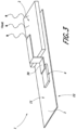
- Figure 1A is a schematic perspective view of a connector 1, according to various embodiments.
- Figure 1B is a schematic side cross-sectional view of a portion of the connector 1.
- the connector 1 is configured to provide electronic communication (including, e.g ., data communication and/or electrical power) between a first electronic device and a second electronic device.
- the first electronic device can comprise a computing device (such as a laptop computer, a desktop computer, a smartphone, a tablet computing device, etc.), an imaging system, an audio system, etc.
- the second electronic device can comprise another device, e.g., peripheral, electronic or computing device, an external mouse or keyboard, a memory device (such as a portable memory stick), power supply electronics (for a power cord), an imaging system, an audio system, and/or any other suitable types of peripheral devices.
- the connector 1 can conform to the USB standards as set forth at usb.org, such as USB 2.0 or USB 3.1.
- the connector 1 comprises a substrate 3 and an interface member 2 mounted to an upper surface 11 of the substrate 3.
- the interface member 2 which is illustrated schematically as a simple block, can comprise various I/O terminals that provide data communication to and/or from the electronic device ( e.g. , by way of one or more data lines), and/or that provide power to and/or draw power from the electronic device ( e.g., by way of one or more power lines).
- the interface member 2 can be removeably inserted into (or can receive) a corresponding portion of the electronic device so as to provide mechanical connection and electronic communication between the first and second electronic devices.
- the interface member 2 may comprise suitable mechanical connections or latches to mechanically connect to the electronic device, as well as I/O terminals for data and/or electrical communication with the electronic device.
- the connector 1 can be formed at the terminal end of a cable (e.g., a USB cable), or can extend integrally from one of the electronic devices (e.g., from a memory stick).
- the substrate 3, in turn, can electrically connect the connector 1 with the cable wiring or the electronic device with which the connector is integrated.
- the substrate 3 can comprise one or more patterned layers, e.g ., a non-conductive material 6 and a conductive material comprising one or more conductors (e.g., first and second conductors 10, 15) formed with and/or embedded in the non-conductive material 6.
- the substrate 3 can comprise a laminate substrate, such as a PCB substrate, in which the conductors 10, 15 may be embedded in the non-conductive material 6 (such as FR-4 or FR-5 board).
- the substrate 3 may comprise a flexible substrate.
- the substrate 3 may comprise any suitable type of material, such as a ceramic non-conductive material formed with the one or more conductors.
- the first and second conductors 10, 15 can act as metallic traces and/or contact pads to transfer signals between the interface member 2 and the first electronic device ( e.g., by way of a cable extending from the interface member 2 to the second electronic device).
- the connector 1 can comprise a thermally resettable fuse 18.
- the fuse 18 of Figures 1A and 1B can include a PTC material 4 sandwiched between a first metal electrode 17a and a second metal electrode 17b.
- the PTC material 4 can comprise a polymer material filled with conductive particles (e . g ., carbon black) that conducts under normal operating conditions but becomes insulating above a trip threshold temperature.
- the fuse 18 may exhibit hysteresis behavior such that the fuse 18 can become conducting once the temperature falls below a reset threshold.
- the two electrodes 17a, 17b and the PTC material 4 form the fuse 18, which is disposed directly below and horizontally overlapping with the interface member 2.
- the PTC material 4 can be positioned as closely as possible to the interface member 2 (which connects to the larger electronic device) such that there is high thermal conductivity between the PTC material 4 of the fuse 18 and the interface member 2. If, on the other hand, the PTC material 4 is positioned at a large distance from the connector 1, then the temperature of the PTC material 4 may be significantly different from the temperature of the connector 1. Thus, as shown in Figures 1A-1B , at least a portion of the fuse 18 can be positioned directly below the interface member 2 such that a plane perpendicular to the substrate 3 passes through the interface member 2 and at least a portion of the PTC material 4.
- the fuse 18 can be smaller than, larger than, or about the same size as the substrate 3.
- the fuse 18 may be sufficiently sized relative to the substrate 3 so as to provide at least partial lateral overlap between the fuse 18 and the substrate 3.
- the fuse 18 can be completely embedded in the substrate 3 such that the fuse 18 is not exposed at the upper surface 11 of the substrate 3. In such arrangements, for example, the fuse 18 can be sandwiched between different layers of the non-conductive material 6
- the fuse 18 can be electrically connected with the first conductor 10 and the interface member 2.
- the interface member 2 (shown schematically in dashed lines in Figure 1B ) can electrically connect to a contact pad 8 of the first conductor 10 that is exposed on the upper surface 11 of the substrate 3.
- the interface member 2 can be attached to the contact pad 8 with any suitable conductive interconnect 16, such as solder, conductive epoxy, etc.
- a first conductive via 7a can pass through the non-conductive material 6 to expose the first electrode 17a of the fuse 18, such that the first conductor 10 provides electrical communication between the interface member 2 and the fuse 18.
- a second conductor 15 can be formed with the non-conductive material 6 and a second via 7b can pass through the non-conductive material 6 to expose the second electrode 17b of the fuse 18, such that the second conductor 15 provides electrical communication between the fuse 18 and the second electronic device.
- the second conductor 15 can be disposed at or near a lower surface 12 of the substrate 3.
- the first and second conductors 10, 15 can form part of a power line that supplies electrical current through the connector 1 between the first electronic device and the second electronic device.
- current can flow between the interface member 2 and the second conductor 15 by way of the contact pad 8, the first via 7a, the first electrode 17a of the fuse 18, the PTC material 4 of the fuse 18, the second electrode 17b of the fuse 18 and the second via 7b.
- the second conductor 15 can convey the current to and/or from the second electronic device.
- the interface member 2 can convey the current to and/or from the first electronic device to which the connector 1 is to be connected.
- the first conductive via 7a can provide a short thermal pathway by which the PTC element 4 can be heated.
- the temperature of the PTC material 4 can closely track the temperature of the interface member 2 and significant heat can be transferred even through the non-conductive material 6.
- the fuse 18 can be spaced below the interface member 2 by a distance ( e .
- the fuse 18 can be spaced below the interface member 2 by a distance such that the difference in temperature between the interface member 2 and the PTC element 4 during operation is in a range of 5 °C to 20 °C, in a range of 5°C to 15 °C, or in a range of 8 °C to 12 °C.
- the fuse 18 can be spaced below the interface member 2 by a distance such that the difference in temperature between the interface member 2 and the PTC element 4 during operation is in a range of 40 °C to 50 °C, or in a range of 43°C to 50 °C.
- the PTC element 4 can be spaced below the interface member 2 by a distance less than 5 mm, or more particularly, by a distance less than 3 mm, e.g., by a distance less than 1 mm.
- the PTC element 4 can be spaced below the interface member 2 by a distance in a range of 0.1 mm to 5 mm, in a range of 0.1 mm to 3 mm, in a range of 0.1 mm to 2 mm, in a range of 0.1 mm to 1 mm, in a range of 0.2 mm to 1 mm, in a range of 0.3 mm to 1 mm, in a range of 0.3 mm to 0.9 mm, in a range of 0.4 mm to 1 mm, or in a range of 0.4 mm to 0.9 mm.
- the fuse 18 can have a low resistance state and a high resistance state, such that the fuse 18 is configured to move from the low resistance state to the high resistance state when the temperature of the interface member 2 exceeds a predetermined temperature.
- the predetermined temperature of the interface member 2 can be in a range of 65 °C to 170 °C, in a range of 65 °C to 120 °C, in a range of 70 °C to 100 °C, in a range of 65 °C to 90 °C, in a range of 65 °C to 80 °C, or in a range of 68 °C to 72 °C.
- the predetermined temperature of the interface member 2 can be in a range of 100 °C to 170 °C, in a range of 110 °C to 150 °C, or in a range of 115 °C to 125 °C.
- the fuse 18 may exhibit asymmetrical hysteresis properties such that the fuse 18 can be configured to move from the high resistance state to the low resistance state when a second predetermined temperature of the interface member 2 is less than 50 °C, e.g. , less than 40 °C.
- the fuse 18 can be configured to move from the high resistance state to the low resistance state when the predetermined temperature of the interface member 2 is in a range of 20 °C to 50 °C, in a range of 25°C to 40 °C, or in a range of 30 °C to 40 °C.
- the fuse 18 can have a low resistance state and a high resistance state, such that the fuse 18 is configured to move from the low resistance state to the high resistance state when the temperature of the fuse 18 exceeds a predetermined temperature.
- the predetermined temperature of the fuse 18 can be in a range of 65 °C to 170 °C, in a range of 65 °C to 120 °C, in a range of 70 °C to 100 °C, in a range of 65 °C to 90 °C, in a range of 65 °C to 80 °C, or in a range of 68 °C to 72 °C.
- the predetermined temperature of the interface member 2 can be in a range of 100 °C to 170 °C, in a range of 110 °C to 150 °C, or in a range of 115 °C to 125 °C.
- the fuse 18 can be configured to move from the high resistance state to the low resistance state when a second predetermined temperature of the fuse 18 is less than 55 °C, e.g., less than 50 °C.
- the fuse 18 can be configured to move from the high resistance state to the low resistance state when the predetermined temperature of the fuse 18 is in a range of 25 °C to 55 °C, in a range of 30 °C to 50 °C, or in a range of 35°C to 45 °C.
- the resistance of the fuse 18 may accordingly increase so as to significantly impede current from flowing through the PTC material 4.
- the high resistance of the PTC material 4 in the fault condition or state may act to protect the electronic device and/or the peripheral device.
- the temperature of the PTC material 4 also subsides.
- the drop in temperature of the PTC material 4 can accordingly decrease the resistance of the fuse 18, enabling more current to pass through the fuse 18 between the interface member 2 and the second conductor 15.
- one or more data lines may be provided in the substrate 3 to transmit data between the interface member 2 and the peripheral device.
- the one or more data lines may be provided at or near the upper surface 11 of the substrate.
- the data line(s) may be provided along or near the upper surface 11, and the power line(s) may extend into the substrate 3, e.g., from the contact pad 8 at or near the upper surface 11 to the second conductor 15 at or near the lower surface 12.
- the second conductor 15 is illustrated as being disposed at or near the lower surface 12, in some embodiments, the second conductor 15 can be embedded within the substrate 3.
- one or more insulating layers such as FR-4 board
- the current from the second conductor 15 may be routed back to at or near the upper surface 11, e.g., by way of one or more vias 19 and traces 21 (see Figure 2B ).
- Figure 2A is a schematic top plan view of a substrate 3, according to various embodiments.
- Figure 2B is a schematic side cross-section of the substrate 3 shown in Figure 2A .
- the interface member 2 is not shown in Figures 2A-2B .
- the reference numerals of Figures 2A-2B represent components that are the same as or similar to the components shown in Figures 1A-1B .
- Figure 2A illustrates that one or more additional electrical components 20 (such as integrated device dies, active components, passive components such as capacitors, resistors, etc.) can be provided on the substrate 3 of the connector 1.
- the electrical components 20 can be configured to control the operation of the connector 1 and how the connector 1 interfaces with the peripheral device and/or the electronic device.
- various types of integrated device dies such as controller dies
- active components such as active components
- passive components can be provided on the substrate 3.
- various resistors, capacitors, inductors, diodes, and control chips can be provided on the substrate 3 as surface mount devices.
- one or more vias 19 can route electrical signals from the second conductor 15 back to a trace 21 at or near the upper surface of the substrate 3.
- Figure 3 is a schematic perspective view of a connector 1, according to another embodiment.
- the reference numerals of Figure 3 represent components that are the same as or similar to the components shown in Figures 1A-2B .
- the connector 1 can comprise an interface member 2 mounted to a substrate 3.
- the fuse 18 can be mounted to the upper surface 11 of the substrate 3 and can be laterally displaced relative to the interface member 2.
- a conductive tab 30 can be provided to thermally connect the fuse 18 and the interface member 2.
- the conductive tab 30 can be provided over an upper surface of the substrate 3. In some embodiments, the conductive tab 30 may contact an upper surface of the substrate 3.
- the conductive tab 30 may not contact the substrate 3 but may instead be vertically offset over the upper surface of the substrate 3.
- the conductive tab 30 can be wrapped around portions of the fuse 18 and the interface member 2.
- the conductive tab 30 can comprise any suitable type of conductor, such as nickel.
- the tab 30 can beneficially provide a direct thermally conductive pathway between the interface member 2 and the PTC element 4 such that the temperature of the fuse 18 closely tracks the temperature of the interface member 2.
- the fuse 18 can be placed in close proximity to the interface member 2 so as to ensure that the temperature of the fuse 18 is as close as possible to the temperature of the interface member 2.
- the fuse 18 can be laterally spaced from the interface member 2 by a separation distance in a range of 0.1 mm to 0.8 mm, in a range of 0.1 mm to 0.5 mm, or in a range of 0.1 mm to 0.3 mm, e.g ., about 0.2 mm in some embodiments, or about 0.6 mm in some embodiments.
- the conductive tab 30 can be bent or shaped to conform to the surfaces of the interface member 2, the substrate 3, and/or the fuse 18.
- the conductive tab 30 can connect to an upper surface of the interface member 2, can be bent or angled downwardly along a side wall of the interface member 2, and can be further angled laterally outward to connect to the fuse 18.
- Figure 4 is a schematic perspective view of a connector 1 coupled with a cable 25, according to various embodiments.
- the interface member 2 can be disposed inside an encapsulating material 26.
- a distal end portion of the interface member 2 can extend distally outside and beyond the encapsulating material 26.
- the distally-extending portion of the interface member 2 can comprise a male connector to electrically and/or electronically connect to the electronic device.
- the connector 1 can be sized and configured to conform to any suitable standard, such as the USB standard(s), as explained above.
- the connector 1 can be dimensioned to comply with the USB standard(s).
- a width w of the interface member 2 can be in a range of 5 mm to 15 mm, in a range of 7 mm to 14 mm, in a range of 8 mm to 13 mm.
- the width w can be in a range of 6 mm to 7 mm, in a range of 8 mm to 9 mm, or in a range of 11 mm to 13 mm.
- a height h of the interface member 2 can be in a range of 1 mm to 12 mm, e.g., in a range of 4 mm to 5 mm, in a range of 7 mm to 8 mm, in a range of 10 mm to 11 mm, in a range of 1.5 mm to 3.5 mm, or in a range of 2 mm to 3 mm.
Description
- The field relates to a connector with an integrated resettable thermal fuse, and in particular to a connector with an integrated positive temperature coefficient (PTC) fuse.
- Various types of electronic devices can include one or more ports that enable the electronic device to be connected to assorted peripheral devices. An electronic device or a computing device (such as a laptop computer, a desktop computer, a smartphone, a tablet computing device, etc.) can include a port that connects to a cable associated with a desired peripheral device. For example, the peripheral device may comprise another computing device, an external mouse or keyboard, a memory device (such as a portable memory stick), power supply electronics (such as a transformer for a power cord), and/or any other suitable types of peripheral devices.
- When the cable is inserted into the port, data can be exchanged between the peripheral device and the electronic device along one or more data lines of the cable, and/or electrical power can be transferred between the peripheral device and the electronic device along one or more power lines of the cable. In some arrangements, the transfer of electrical energy along the cable can result in overheating and/or excessive current within the electronic device and/or the peripheral device. Such overheating and/or overcurrent conditions may damage the electronic device and/or the peripheral device.
Documents EP 2 372 827 A1 ,US 2011/003179 A1 andUS 2015/0288110 A1 described connectors with thermal protection circuit in the power line. However, there remains a continuing need to reduce or eliminate damage caused by excessive temperature and/or current in the cable. - A connector for providing electronic communication with an electronic device is disclosed. The connector can include a substrate comprising patterned layers of non-conductive material and conductive material. The connector can include an interface member mounted on the substrate and electrically connected with the conductive material. A positive temperature coefficient (PTC) fuse can be embedded in the substrate and electrically connected with the conductive material and the interface member. At least a portion of the PTC fuse can be disposed directly below the interface member.
- A connector according to the present invention for providing electronic communication with an electronic device is as defined by the appended claims. The connector includes a substrate comprising patterned layers of non-conductive material and conductive material. The connector includes an interface member mounted on the substrate and electrically connected with the conductive material. The connector includes a resettable thermal fuse embedded in the substrate and electrically connected with the conductive material and the interface member. At least a portion of the resettable thermal fuse is disposed directly below the interface member.
- A connector for providing electronic communication with an electronic device is disclosed. The connector can comprise a substrate comprising patterned layers of non-conductive material and conductive material. The connector includes an interface member mounted on an upper surface of the substrate and electrically connected with the conductive material. The connector can comprise a resettable thermal fuse mounted to the upper surface of the substrate and electrically connected with the conductive material and the interface member, the resettable thermal fuse laterally offset in close proximity to the interface member. The connector can include a conductive tab providing electrical communication between the interface member and the resettable thermal fuse, the conductive tab disposed over an upper surface of the substrate.
- A method for manufacturing a connector, which is not covered by the present invention, is disclosed. The method can include providing a substrate comprising patterned layers of non-conductive material and conductive material and a resettable thermal fuse embedded in the substrate and electrically connected with the conductive material. The method can include mounting an interface member on the substrate. The method can include electrically connecting the interface member with the conductive material and the resettable thermal fuse. At least a portion of the resettable thermal fuse can be disposed directly below the interface member.
- These and other embodiments will become readily apparent to those skilled in the art from the following detailed description of the preferred embodiments having reference to the attached figures, the invention not being limited to any particular preferred embodiment(s) disclosed.
- Specific implementations of the invention will now be described with reference to the following drawings, which are provided by way of example, and not limitation.
-
Figure 1A is a schematic perspective view of a connector, according to various embodiments. -
Figure 1B is a schematic side cross-sectional view of a portion of the connector shown inFigure 1A . -
Figure 2A is a schematic top plan view of a substrate, according to various embodiments. -
Figure 2B is a schematic side cross-section of the substrate shown inFigure 2A . -
Figure 3 is a schematic perspective view of a connector, according to another embodiment. -
Figure 4 is a schematic perspective view of a connector coupled with a cable, according to various embodiments. - Various embodiments disclosed herein relate to a connector with an integrated thermally resettable fuse, e.g., a positive temperature coefficient (PTC) element or fuse. For example, as explained above, various types of electronic devices can exchange data with a peripheral device along one or more data lines and can transfer power with the peripheral device along one or more power lines. In such devices, it can be important to ensure that the connector does not experience excessive temperatures and/or currents in order to reduce the risk of damage to the larger electronic device and/or to the peripheral device. Note that references to larger devices and peripheral devices herein are merely examples and not intended to be limiting. The skilled artisan will appreciate that connectors as described herein can be employed in numerous different applications, including data/power cables, such as USB cables, which can connect any of a number of different types of devices. It will also be understood that, while described as serving to connect first and second electronic devices in operation, that the connector described herein can exist in a cable, such as a USB cable, which may be unconnected to any electronic devices.
- In some embodiments, for example, the connector can include a substrate comprising a non-conductive material and a conductor formed with the non-conductive material. For example, in some embodiments, the substrate can comprise a printed circuit board (PCB) in which layers of nonconductive material (e.g., FR4 or FR5, also known as "prepreg") and conductive material (e.g., metal, such as copper) are laminated together. The connector can also include an interface member mounted to the substrate and electrically connected with the conductor. The interface member can comprise various input-output (I/O) terminals that provide data communication to and/or from the electronic device (e.g., by way of one or more data lines), and/or that provide power to and/or draw power from the electronic device (e.g., by way of one or more power lines). The connector can also include a positive temperature coefficient (PTC) element embedded in the substrate and electrically connected with the conductor and the interface member. At least a portion of the PTC element can be disposed directly below the interface member.
- The connector disclosed herein can be used with cables and devices that utilize the Universal Serial Bus (USB) standard. For example, the connector disclosed herein can be incorporated into a cable having one or more data lines and/or one or more power lines. The embodiments disclosed herein can be used with any suitable version of the USB standard. As an example, the disclosed embodiments can be used in connection with USB 2.0, in which four I/O terminals (two for power and two for data) are used. The disclosed embodiments may also be used in USB 3.1 in which 10 I/O terminals (8 for data and 2 for power) are provided. In some arrangements, the disclosed embodiments can be used in connection with USB 3.0 as well. Indeed, the connector disclosed herein can be utilized with any suitable version of USB, and indeed with cables and devices conforming to other standards. The connector can be removably inserted into an electronic device to transfer data to and/or from the electronic device over the data line(s), and to supply power to and/or draw power from the electronic device over the power line(s). In other embodiments, the connector may be incorporated into a device other than a cable, such as a memory stick, a computing device, etc. Thus, in some embodiments, the connector may be integrated with a cable, and in other embodiments, the connector may be integrated with a particular electronic device. In various embodiments, the connector may comprise a male connector. In other embodiments, the connector may comprise a female connector.
- In various arrangements, the connector may experience elevated temperature and/or excessive current. For example, surges in current along the power line(s) may damage the electronic device and/or the peripheral device that is connected to the electronic device. One way to mitigate or prevent damage to the electronic device and/or the peripheral device is to incorporate a positive temperature coefficient (PTC) element, which serves as a resettable fuse, into the connector. The fuse can incorporate a PTC material, in which the resistivity of a normally conductive material increases as the temperature of the material increases. Examples of such a material used in PTC elements are organic polymers, made electrically conductive by dispersing conductive fillers therein. These polymers may include polyolefins such as polyethylene, polypropylene and ethylene/propylene copolymers. Conductive fillers can include carbon black and metal powders. In some arrangements, a PTC fuse comprises a layer of conductive polymer PTC material sandwiched between conductive layers, e.g., between upper and lower metal foil electrodes.
- At temperatures below a predetermined value, a PTC element may exhibit a relatively low resistivity (which may be relatively constant). However, as the temperature of the PTC element increases beyond the predetermined temperature, the resistivity of the material of the PTC element sharply increases with temperature. In various embodiments, for example, the resistivity may increase to such an extent so as to significantly impede current from passing through the PTC element. Wien the temperature of the material in the PTC element cools down below the predetermined temperature, the resistivity reverts to its lower value such that electrical current can pass through without significant losses. Due to the hysteresis properties of the PTC element, therefore, the PTC element can be used in a first, normal operating state in which current passes through the PTC element with little resistance. If the temperature of the PTC element rises above the predetermined temperature so as to indicate an overtemperature or overcurrent condition, then the PTC element switches to a second, fault state in which little to no current passes through the PTC element to protect the connected device(s). Once the temperatures drop to desired levels, the PTC element can revert to the normal operating state. In various embodiments, the predetermined temperature at which the PTC element switches from the first state to the second state is in a range of 65°C to 170°C. In some embodiments, the predetermined temperature at which the PTC element switches from the first state to the second state is in a range of 65°C to 90°C, in a range of 65°C to 80°C, or in a range of 68°C to 72°C. In some embodiments, the predetermined temperature at which the PTC element switches from the first state to the second state is in a range of 100°C to 170°C, in a range of 110°C to 150°C, or in a range of 115°C to 125°C. In various arrangements, temperature and/or current can be used to define when the PTC element switches from the first state to the second state. For example, the PTC element can switch from the first state to the second state at a current in a range of 1A to 5A, in a range of 2A to 4A, or in a range of 2.5A to 3.5A. Additional details of PTC elements or materials that can be used in conjunction with any of the disclosed embodiments may be found throughout U.S. Patent Publication No.
US 2006/0055501 , the disclosure of which is incorporated by reference herein in its entirety and for all purposes. -
Figure 1A is a schematic perspective view of aconnector 1, according to various embodiments.Figure 1B is a schematic side cross-sectional view of a portion of theconnector 1. Theconnector 1 is configured to provide electronic communication (including, e.g., data communication and/or electrical power) between a first electronic device and a second electronic device. As explained above, the first electronic device can comprise a computing device (such as a laptop computer, a desktop computer, a smartphone, a tablet computing device, etc.), an imaging system, an audio system, etc. The second electronic device can comprise another device, e.g., peripheral, electronic or computing device, an external mouse or keyboard, a memory device (such as a portable memory stick), power supply electronics (for a power cord), an imaging system, an audio system, and/or any other suitable types of peripheral devices. In some embodiments, theconnector 1 can conform to the USB standards as set forth at usb.org, such as USB 2.0 or USB 3.1. - The
connector 1 comprises asubstrate 3 and aninterface member 2 mounted to anupper surface 11 of thesubstrate 3. Theinterface member 2, which is illustrated schematically as a simple block, can comprise various I/O terminals that provide data communication to and/or from the electronic device (e.g., by way of one or more data lines), and/or that provide power to and/or draw power from the electronic device (e.g., by way of one or more power lines). In various embodiments, theinterface member 2 can be removeably inserted into (or can receive) a corresponding portion of the electronic device so as to provide mechanical connection and electronic communication between the first and second electronic devices. Thus, theinterface member 2 may comprise suitable mechanical connections or latches to mechanically connect to the electronic device, as well as I/O terminals for data and/or electrical communication with the electronic device. Theconnector 1 can be formed at the terminal end of a cable (e.g., a USB cable), or can extend integrally from one of the electronic devices (e.g., from a memory stick). Thesubstrate 3, in turn, can electrically connect theconnector 1 with the cable wiring or the electronic device with which the connector is integrated. - As shown in
Figure 1B , thesubstrate 3 can comprise one or more patterned layers, e.g., anon-conductive material 6 and a conductive material comprising one or more conductors (e.g., first andsecond conductors 10, 15) formed with and/or embedded in thenon-conductive material 6. In some embodiments, thesubstrate 3 can comprise a laminate substrate, such as a PCB substrate, in which theconductors substrate 3 may comprise a flexible substrate. In other embodiments, thesubstrate 3 may comprise any suitable type of material, such as a ceramic non-conductive material formed with the one or more conductors. The first andsecond conductors interface member 2 and the first electronic device (e.g., by way of a cable extending from theinterface member 2 to the second electronic device). - As shown in
Figures 1A and1B , theconnector 1 can comprise a thermallyresettable fuse 18. Thefuse 18 ofFigures 1A and1B can include a PTC material 4 sandwiched between afirst metal electrode 17a and asecond metal electrode 17b. For example, the PTC material 4 can comprise a polymer material filled with conductive particles (e.g., carbon black) that conducts under normal operating conditions but becomes insulating above a trip threshold temperature. As explained above, thefuse 18 may exhibit hysteresis behavior such that thefuse 18 can become conducting once the temperature falls below a reset threshold. Together the twoelectrodes fuse 18, which is disposed directly below and horizontally overlapping with theinterface member 2. It can be important to position the PTC material 4 as closely as possible to the interface member 2 (which connects to the larger electronic device) such that there is high thermal conductivity between the PTC material 4 of thefuse 18 and theinterface member 2. If, on the other hand, the PTC material 4 is positioned at a large distance from theconnector 1, then the temperature of the PTC material 4 may be significantly different from the temperature of theconnector 1. Thus, as shown inFigures 1A-1B , at least a portion of thefuse 18 can be positioned directly below theinterface member 2 such that a plane perpendicular to thesubstrate 3 passes through theinterface member 2 and at least a portion of the PTC material 4. In some embodiments, only a portion of thefuse 18 is disposed directly below theinterface member 2, and another portion of thefuse 18 is disposed laterally outside theinterface member 2. In other embodiments, theentire fuse 18 is disposed directly below theinterface member 2. In some embodiments, thefuse 18 can be smaller than, larger than, or about the same size as thesubstrate 3. For example, in some embodiments, thefuse 18 may be sufficiently sized relative to thesubstrate 3 so as to provide at least partial lateral overlap between thefuse 18 and thesubstrate 3. - In some embodiments, the
fuse 18 can be completely embedded in thesubstrate 3 such that thefuse 18 is not exposed at theupper surface 11 of thesubstrate 3. In such arrangements, for example, thefuse 18 can be sandwiched between different layers of thenon-conductive material 6 Thefuse 18 can be electrically connected with thefirst conductor 10 and theinterface member 2. For example, the interface member 2 (shown schematically in dashed lines inFigure 1B ) can electrically connect to acontact pad 8 of thefirst conductor 10 that is exposed on theupper surface 11 of thesubstrate 3. For example, theinterface member 2 can be attached to thecontact pad 8 with any suitableconductive interconnect 16, such as solder, conductive epoxy, etc. A first conductive via 7a can pass through thenon-conductive material 6 to expose thefirst electrode 17a of thefuse 18, such that thefirst conductor 10 provides electrical communication between theinterface member 2 and thefuse 18. - Further, as shown in
Figure 1B , asecond conductor 15 can be formed with thenon-conductive material 6 and a second via 7b can pass through thenon-conductive material 6 to expose thesecond electrode 17b of thefuse 18, such that thesecond conductor 15 provides electrical communication between thefuse 18 and the second electronic device. As shown inFigure 1B , thesecond conductor 15 can be disposed at or near alower surface 12 of thesubstrate 3. - In the embodiment of
Figures 1A-1B , the first andsecond conductors connector 1 between the first electronic device and the second electronic device. For example, in operation, current can flow between theinterface member 2 and thesecond conductor 15 by way of thecontact pad 8, the first via 7a, thefirst electrode 17a of thefuse 18, the PTC material 4 of thefuse 18, thesecond electrode 17b of thefuse 18 and the second via 7b. Thesecond conductor 15 can convey the current to and/or from the second electronic device. Theinterface member 2 can convey the current to and/or from the first electronic device to which theconnector 1 is to be connected. - If the
interface member 2 experiences excessive temperature and/or current, the first conductive via 7a can provide a short thermal pathway by which the PTC element 4 can be heated. Beneficially, positioning at least a portion of thefuse 18 directly below and in close proximity to theinterface member 2, the temperature of the PTC material 4 can closely track the temperature of theinterface member 2 and significant heat can be transferred even through thenon-conductive material 6. For example, in various embodiments, the fuse 18 can be spaced below the interface member 2 by a distance (e.g., defined between an upper surface of the fuse 18 and a lower surface of the interface member 2) such that the difference in temperature between the interface member 2 and the PTC element 4 during operation is in a range of 5 °C to 55 °C, or more particularly in a range of 10 °C to 50 °C, e.g., in a range of 10 °C to 40 °C. In some embodiments, the fuse 18 can be spaced below the interface member 2 by a distance such that the difference in temperature between the interface member 2 and the PTC element 4 during operation is in a range of 5 °C to 20 °C, in a range of 5°C to 15 °C, or in a range of 8 °C to 12 °C. In some embodiments, the fuse 18 can be spaced below the interface member 2 by a distance such that the difference in temperature between the interface member 2 and the PTC element 4 during operation is in a range of 40 °C to 50 °C, or in a range of 43°C to 50 °C. In some embodiments, the PTC element 4 can be spaced below the interface member 2 by a distance less than 5 mm, or more particularly, by a distance less than 3 mm, e.g., by a distance less than 1 mm. For example, the PTC element 4 can be spaced below theinterface member 2 by a distance in a range of 0.1 mm to 5 mm, in a range of 0.1 mm to 3 mm, in a range of 0.1 mm to 2 mm, in a range of 0.1 mm to 1 mm, in a range of 0.2 mm to 1 mm, in a range of 0.3 mm to 1 mm, in a range of 0.3 mm to 0.9 mm, in a range of 0.4 mm to 1 mm, or in a range of 0.4 mm to 0.9 mm. - As explained herein, the
fuse 18 can have a low resistance state and a high resistance state, such that thefuse 18 is configured to move from the low resistance state to the high resistance state when the temperature of theinterface member 2 exceeds a predetermined temperature. The predetermined temperature of the interface member 2 can be in a range of 65 °C to 170 °C, in a range of 65 °C to 120 °C, in a range of 70 °C to 100 °C, in a range of 65 °C to 90 °C, in a range of 65 °C to 80 °C, or in a range of 68 °C to 72 °C. In some embodiments, the predetermined temperature of the interface member 2 can be in a range of 100 °C to 170 °C, in a range of 110 °C to 150 °C, or in a range of 115 °C to 125 °C. The fuse 18 may exhibit asymmetrical hysteresis properties such that the fuse 18 can be configured to move from the high resistance state to the low resistance state when a second predetermined temperature of the interface member 2 is less than 50 °C, e.g., less than 40 °C. For example, the fuse 18 can be configured to move from the high resistance state to the low resistance state when the predetermined temperature of the interface member 2 is in a range of 20 °C to 50 °C, in a range of 25°C to 40 °C, or in a range of 30 °C to 40 °C. - In some embodiments, the
fuse 18 can have a low resistance state and a high resistance state, such that thefuse 18 is configured to move from the low resistance state to the high resistance state when the temperature of thefuse 18 exceeds a predetermined temperature. The predetermined temperature of thefuse 18 can be in a range of 65 °C to 170 °C, in a range of 65 °C to 120 °C, in a range of 70 °C to 100 °C, in a range of 65 °C to 90 °C, in a range of 65 °C to 80 °C, or in a range of 68 °C to 72 °C. In some embodiments, the predetermined temperature of theinterface member 2 can be in a range of 100 °C to 170 °C, in a range of 110 °C to 150 °C, or in a range of 115 °C to 125 °C. Thefuse 18 can be configured to move from the high resistance state to the low resistance state when a second predetermined temperature of thefuse 18 is less than 55 °C, e.g., less than 50 °C. For example, thefuse 18 can be configured to move from the high resistance state to the low resistance state when the predetermined temperature of thefuse 18 is in a range of 25 °C to 55 °C, in a range of 30 °C to 50 °C, or in a range of 35°C to 45 °C. - As the temperature of the PTC material 4 rises above the predetermined temperature, the resistance of the
fuse 18 may accordingly increase so as to significantly impede current from flowing through the PTC material 4. The high resistance of the PTC material 4 in the fault condition or state may act to protect the electronic device and/or the peripheral device. As the overcurrent or overtemperature fault condition subsides, the temperature of the PTC material 4 also subsides. The drop in temperature of the PTC material 4 can accordingly decrease the resistance of thefuse 18, enabling more current to pass through thefuse 18 between theinterface member 2 and thesecond conductor 15. - Although only a single power line is shown (with respect to the
conductors 10, 15), in various embodiments, additional power lines may be provided, for example, so as to provide a ground line and a power supply line. Moreover, although not illustrated, one or more data lines may be provided in thesubstrate 3 to transmit data between theinterface member 2 and the peripheral device. For example, in some embodiments, the one or more data lines may be provided at or near theupper surface 11 of the substrate. Thus, in some arrangements, the data line(s) may be provided along or near theupper surface 11, and the power line(s) may extend into thesubstrate 3, e.g., from thecontact pad 8 at or near theupper surface 11 to thesecond conductor 15 at or near thelower surface 12. Although thesecond conductor 15 is illustrated as being disposed at or near thelower surface 12, in some embodiments, thesecond conductor 15 can be embedded within thesubstrate 3. For example, in some embodiments, one or more insulating layers (such as FR-4 board) can be disposed underneath and above thesecond conductor 15. In some embodiments, moreover, the current from thesecond conductor 15 may be routed back to at or near theupper surface 11, e.g., by way of one ormore vias 19 and traces 21 (seeFigure 2B ). - U.S. Patent Publication No.
US 2006/0055501 ("the '501 publication") teaches a method of forming afuse 18 using PCB technology. The process can be used to form the embeddedfuse 18 taught herein by omitting the portions of the process of the '501 publication that singulate fuses to form surface mount devices. Instead, thefuse 18 can remain embedded within the PCB material and the remainder of thesubstrate 3 can be processed as normal for routing signal and power lines and interconnecting surface mounted devices as shown inFigures 2A and 2B , discussed below. -
Figure 2A is a schematic top plan view of asubstrate 3, according to various embodiments.Figure 2B is a schematic side cross-section of thesubstrate 3 shown inFigure 2A . Theinterface member 2 is not shown inFigures 2A-2B . Unless otherwise noted, the reference numerals ofFigures 2A-2B represent components that are the same as or similar to the components shown inFigures 1A-1B .Figure 2A illustrates that one or more additional electrical components 20 (such as integrated device dies, active components, passive components such as capacitors, resistors, etc.) can be provided on thesubstrate 3 of theconnector 1. Theelectrical components 20 can be configured to control the operation of theconnector 1 and how theconnector 1 interfaces with the peripheral device and/or the electronic device. For example, various types of integrated device dies (such as controller dies), active components, and/or passive components can be provided on thesubstrate 3. In some arrangements, various resistors, capacitors, inductors, diodes, and control chips can be provided on thesubstrate 3 as surface mount devices. Moreover, as shown inFigure 2B , in some embodiments, one ormore vias 19 can route electrical signals from thesecond conductor 15 back to atrace 21 at or near the upper surface of thesubstrate 3. -
Figure 3 is a schematic perspective view of aconnector 1, according to another embodiment. Unless otherwise noted, the reference numerals ofFigure 3 represent components that are the same as or similar to the components shown inFigures 1A-2B . For example, theconnector 1 can comprise aninterface member 2 mounted to asubstrate 3. Unlike the embodiment ofFigures 1 A-2B , however, thefuse 18 can be mounted to theupper surface 11 of thesubstrate 3 and can be laterally displaced relative to theinterface member 2. To enhance thermal conductivity between theinterface member 2 and thefuse 18, aconductive tab 30 can be provided to thermally connect thefuse 18 and theinterface member 2. As shown inFigure 3 , theconductive tab 30 can be provided over an upper surface of thesubstrate 3. In some embodiments, theconductive tab 30 may contact an upper surface of thesubstrate 3. In other embodiments, theconductive tab 30 may not contact thesubstrate 3 but may instead be vertically offset over the upper surface of thesubstrate 3. Theconductive tab 30 can be wrapped around portions of thefuse 18 and theinterface member 2. Theconductive tab 30 can comprise any suitable type of conductor, such as nickel. Thetab 30 can beneficially provide a direct thermally conductive pathway between theinterface member 2 and the PTC element 4 such that the temperature of thefuse 18 closely tracks the temperature of theinterface member 2. Thefuse 18 can be placed in close proximity to theinterface member 2 so as to ensure that the temperature of thefuse 18 is as close as possible to the temperature of theinterface member 2. For example, thefuse 18 can be laterally spaced from theinterface member 2 by a separation distance in a range of 0.1 mm to 0.8 mm, in a range of 0.1 mm to 0.5 mm, or in a range of 0.1 mm to 0.3 mm, e.g., about 0.2 mm in some embodiments, or about 0.6 mm in some embodiments. Moreover, as shown inFigure 3 , theconductive tab 30 can be bent or shaped to conform to the surfaces of theinterface member 2, thesubstrate 3, and/or thefuse 18. For example, theconductive tab 30 can connect to an upper surface of theinterface member 2, can be bent or angled downwardly along a side wall of theinterface member 2, and can be further angled laterally outward to connect to thefuse 18. -
Figure 4 is a schematic perspective view of aconnector 1 coupled with acable 25, according to various embodiments. Theinterface member 2 can be disposed inside an encapsulatingmaterial 26. In some embodiments, as shown inFigure 4 , a distal end portion of theinterface member 2 can extend distally outside and beyond the encapsulatingmaterial 26. For example, the distally-extending portion of theinterface member 2 can comprise a male connector to electrically and/or electronically connect to the electronic device. - As explained above, the
connector 1 can be sized and configured to conform to any suitable standard, such as the USB standard(s), as explained above. For example, theconnector 1 can be dimensioned to comply with the USB standard(s). In various embodiments, a width w of theinterface member 2 can be in a range of 5 mm to 15 mm, in a range of 7 mm to 14 mm, in a range of 8 mm to 13 mm. In some embodiments, the width w can be in a range of 6 mm to 7 mm, in a range of 8 mm to 9 mm, or in a range of 11 mm to 13 mm. A height h of theinterface member 2 can be in a range of 1 mm to 12 mm, e.g., in a range of 4 mm to 5 mm, in a range of 7 mm to 8 mm, in a range of 10 mm to 11 mm, in a range of 1.5 mm to 3.5 mm, or in a range of 2 mm to 3 mm. - Although this invention has been disclosed in the context of certain embodiments and examples, it will be understood by those skilled in the art that the present invention extends beyond the specifically disclosed embodiments to other alternative embodiments and/or uses of the invention and obvious modifications and equivalents thereof. In addition, while several variations of the invention have been shown and described in detail, other modifications will be readily apparent to those of skill in the art based upon this disclosure. It is also contemplated that various combinations or sub-combinations of the specific features and aspects of the embodiments may be made. It should be understood that various features and aspects of the disclosed embodiments can be combined with, or substituted for, one another in order to form varying modes of the disclosed invention. Thus, it is intended that the scope of the present invention herein disclosed should not be limited by the particular disclosed embodiments described above, but should be determined only by a fair reading of the claims that follow.
Claims (15)
- A connector for providing electronic communication with an electronic device, the connector comprising:a substrate (3) comprising patterned layers of non-conductive material and conductive material;an interface member (2) mounted on the substrate (3) and electrically connected with the conductive material; anda resettable thermal fuse (18) embedded in the substrate (3) and electrically connected with the conductive material and the interface member (2),wherein at least a portion of the resettable thermal fuse (3) is disposed directly below the interface member (2),wherein the interface member (2) includes one or more terminals configured to provide at least one or more of power and data communication between the electronic device and another electronic device, andcharacterized in that the interface member (2) is configured to be removeably connected with the electronic device and to provide mechanical connection and electrical communication between the electronic device and the another electronic device.
- The connector of Claim 1, wherein the resettable thermal fuse (18) comprises a positive temperature coefficient (PTC) fuse.
- The connector of any one of Claims 1 to 2, wherein the resettable thermal fuse (18) is completely embedded within the non-conductive material.
- The connector of any one of Claims 1 to 2, wherein a portion of the resettable thermal fuse (18) is disposed directly below the interface member (2), and another portion of the resettable thermal fuse (18) is disposed laterally outside the interface member (2).
- The connector of any one of Claims 1 to 2, wherein the entire resettable thermal fuse (18) is disposed directly below the interface member (2).
- The connector of any one of Claims 1 to 2, wherein the conductive material comprises a contact pad (8) on an upper surface (11) of the substrate (3), the interface member (2) being electrically connected to the contact pad (8).
- The connector of Claim 6, wherein the conductive material comprises a first conductor line (10) and a first via (7a) passing through a first layer of the non-conductive material between the contact pad (8) and a first electrode (17a) of the resettable thermal fuse (18), to provide electrical communication between the interface member (2) and the resettable thermal fuse (18).
- The connector of Claim 7, wherein the conductive material further comprises a second conductor line (15) including a second via (7b) passing through a second layer of the non-conductive material to provide electrical communication to a second electrode (17b) of the resettable thermal fuse (18), wherein the second conductor line (15) is disposed at or near a lower surface (12) of the substrate (3).
- The connector of Claim 8, further comprising a third via (19) and a third conductor line (21) at or near an upper surface of the substrate (3), the third via (19) passing through the non-conductive material to electrically connect to the second conductor line (15) with the third conductor line (21).
- The connector of any one of Claims 1 to 9, wherein the substrate (3) comprises a printed circuit board (PCB).
- The connector of any one of Claims 1 to 10, further comprising one or more data lines configured to convey the data communication to and/or from the electronic device, wherein the one or more data lines are disposed at or near an upper surface of the substrate (3) and in communication with the interface member (2).
- The connector of any one of Claims 1 to 11, further comprising one or more power lines configured to convey electrical power to and/or from the electronic device, wherein the one or more power lines are disposed at or near a lower surface of the substrate (3) and in communication with the resettable thermal fuse (18) and the interface member (2).
- The connector of any one of Claims 1 to 12, wherein the resettable thermal fuse (18) has a low resistance state and a high resistance state, wherein the resettable thermal fuse (18) is configured to move from the low resistance state to the high resistance state when the temperature of the interface member (2) exceeds a predetermined temperature.
- The connector of any one of Claims 1 to 13, further comprising one or more device chips configured to control the operation of the connector.
- A cable for providing electronic communication between a computing device and a peripheral device, the cable comprising the connector of any one of Claims 1 to 14, the connector disposed at an end portion of the cable.
Applications Claiming Priority (2)
| Application Number | Priority Date | Filing Date | Title |
|---|---|---|---|
| US201662369956P | 2016-08-02 | 2016-08-02 | |
| PCT/US2017/044607 WO2018026689A1 (en) | 2016-08-02 | 2017-07-31 | Connector with integrated resettable thermal fuse |
Publications (4)
| Publication Number | Publication Date |
|---|---|
| EP3494581A1 EP3494581A1 (en) | 2019-06-12 |
| EP3494581A4 EP3494581A4 (en) | 2020-07-08 |
| EP3494581B1 true EP3494581B1 (en) | 2024-01-10 |
| EP3494581C0 EP3494581C0 (en) | 2024-01-10 |
Family
ID=61073504
Family Applications (1)
| Application Number | Title | Priority Date | Filing Date |
|---|---|---|---|
| EP17837461.7A Active EP3494581B1 (en) | 2016-08-02 | 2017-07-31 | Connector with integrated resettable thermal fuse |
Country Status (6)
| Country | Link |
|---|---|
| US (1) | US11456565B2 (en) |
| EP (1) | EP3494581B1 (en) |
| JP (2) | JP7291621B2 (en) |
| KR (1) | KR102449996B1 (en) |
| CN (2) | CN115425481A (en) |
| WO (1) | WO2018026689A1 (en) |
Families Citing this family (3)
| Publication number | Priority date | Publication date | Assignee | Title |
|---|---|---|---|---|
| KR102342740B1 (en) * | 2014-09-15 | 2021-12-23 | 삼성전자주식회사 | Method and transmitter for transmitting and receiving a signal |
| KR102449996B1 (en) | 2016-08-02 | 2022-09-30 | 보우린스, 인크. | Connector with integrated resettable thermal fuse |
| DE102021132442A1 (en) | 2021-12-09 | 2023-06-15 | Bayerische Motoren Werke Aktiengesellschaft | Electrical connector and vehicle therewith |
Family Cites Families (33)
| Publication number | Priority date | Publication date | Assignee | Title |
|---|---|---|---|---|
| US5691688A (en) | 1994-07-20 | 1997-11-25 | Therm-O-Disc, Incorporated | PTC device |
| US5712610C1 (en) * | 1994-08-19 | 2002-06-25 | Sony Chemicals Corp | Protective device |
| US5884391A (en) * | 1996-01-22 | 1999-03-23 | Littelfuse, Inc. | Process for manufacturing an electrical device comprising a PTC element |
| JPH11330665A (en) | 1998-05-15 | 1999-11-30 | Rohm Co Ltd | Structure for mounting temperature fuse onto circuit board |
| US6239977B1 (en) * | 1999-05-17 | 2001-05-29 | 3Com Corporation | Technique for mounting electronic components on printed circuit boards |
| TW487272U (en) | 2001-03-20 | 2002-05-11 | Polytronics Technology Corp | Multilayer circuit boards |
| US20060055501A1 (en) * | 2002-12-10 | 2006-03-16 | Bourns., Inc | Conductive polymer device and method of manufacturing same |
| AU2003224689A1 (en) * | 2002-12-11 | 2004-06-30 | Bourns, Inc. | Conductive polymer device and method of manufacturing same |
| EP1573753B1 (en) | 2002-12-11 | 2006-05-31 | Bourns, Inc. | Encapsulated electronic device and method of manufacturing the same |
| ATE357123T1 (en) | 2004-11-11 | 2007-04-15 | Dbk David & Baader Gmbh | ELECTRICAL BOARD HEATING UNIT, ELECTRONIC BOARD AND HEATING METHOD |
| TWI313877B (en) | 2006-11-01 | 2009-08-21 | Polytronics Technology Corp | High voltage over-current protection device |
| US20090027821A1 (en) * | 2007-07-26 | 2009-01-29 | Littelfuse, Inc. | Integrated thermistor and metallic element device and method |
| KR20090081649A (en) * | 2008-01-24 | 2009-07-29 | 엘지이노텍 주식회사 | Method for manufacturing battery pack |
| KR20110002616A (en) | 2009-07-02 | 2011-01-10 | 삼성에스디아이 주식회사 | Protection circuit board and secondary battery and battery pack |
| EP2372827A1 (en) | 2010-03-29 | 2011-10-05 | Samsung SDI Co., Ltd. | Sencodary battery pack |
| US20110236727A1 (en) | 2010-03-29 | 2011-09-29 | Young-Cheol Jang | Secondary battery pack |
| US8982578B2 (en) | 2010-10-14 | 2015-03-17 | Tyco Electronics Corporation | Connector system and assembly having integrated protection circuitry |
| US8842406B2 (en) * | 2012-01-06 | 2014-09-23 | Polytronics Technology Corp. | Over-current protection device |
| CN202475937U (en) | 2012-03-13 | 2012-10-03 | 常州乐士雷利电机有限公司 | Gear motor circuit board protection system |
| CN202697037U (en) | 2012-04-13 | 2013-01-23 | 瑞侃电子(上海)有限公司 | Circuit protection module |
| TWI486988B (en) | 2013-01-31 | 2015-06-01 | Polytronics Technology Corp | Over-current protection device and circuit board containing the same |
| CN203491732U (en) * | 2013-08-13 | 2014-03-19 | 中兴通讯股份有限公司 | Mobile terminal charger |
| JP6249336B2 (en) * | 2013-12-13 | 2017-12-20 | パナソニックIpマネジメント株式会社 | Power cord |
| DE102013114006A1 (en) | 2013-12-13 | 2015-06-18 | Endress + Hauser Conducta Gesellschaft für Mess- und Regeltechnik mbH + Co. KG | circuit board |
| JP6280482B2 (en) * | 2014-04-03 | 2018-02-14 | ホシデン株式会社 | connector |
| KR20150143195A (en) * | 2014-06-13 | 2015-12-23 | 삼성전자주식회사 | Connector device |
| US10574004B2 (en) * | 2014-06-13 | 2020-02-25 | Sony Corporaton | Cable and power supply device |
| CN204289919U (en) * | 2014-12-10 | 2015-04-22 | 博硕科技(江西)有限公司 | Overtemperature protection data transmission device |
| TWI594524B (en) * | 2015-11-03 | 2017-08-01 | 聚鼎科技股份有限公司 | Connector |
| CN205960251U (en) * | 2016-07-11 | 2017-02-15 | 德积科技股份有限公司 | Immediately, listen overheated electric connector |
| KR102449996B1 (en) | 2016-08-02 | 2022-09-30 | 보우린스, 인크. | Connector with integrated resettable thermal fuse |
| US9960545B2 (en) | 2016-10-05 | 2018-05-01 | Littelfuse, Inc. | USB cable with thermal protection |
| US10333294B2 (en) * | 2016-10-05 | 2019-06-25 | Littelfuse, Inc. | USB cable with thermal protection |
-
2017
- 2017-07-31 KR KR1020197004859A patent/KR102449996B1/en active IP Right Grant
- 2017-07-31 CN CN202211021463.7A patent/CN115425481A/en active Pending
- 2017-07-31 CN CN201780048983.8A patent/CN109643595A/en active Pending
- 2017-07-31 EP EP17837461.7A patent/EP3494581B1/en active Active
- 2017-07-31 JP JP2019505495A patent/JP7291621B2/en active Active
- 2017-07-31 WO PCT/US2017/044607 patent/WO2018026689A1/en unknown
- 2017-07-31 US US16/322,736 patent/US11456565B2/en active Active
-
2022
- 2022-08-19 JP JP2022130970A patent/JP2022169666A/en not_active Withdrawn
Also Published As
| Publication number | Publication date |
|---|---|
| CN115425481A (en) | 2022-12-02 |
| EP3494581A4 (en) | 2020-07-08 |
| JP2019525416A (en) | 2019-09-05 |
| KR102449996B1 (en) | 2022-09-30 |
| WO2018026689A1 (en) | 2018-02-08 |
| JP7291621B2 (en) | 2023-06-15 |
| JP2022169666A (en) | 2022-11-09 |
| KR20190037266A (en) | 2019-04-05 |
| US20210384683A1 (en) | 2021-12-09 |
| EP3494581A1 (en) | 2019-06-12 |
| EP3494581C0 (en) | 2024-01-10 |
| CN109643595A (en) | 2019-04-16 |
| US11456565B2 (en) | 2022-09-27 |
Similar Documents
| Publication | Publication Date | Title |
|---|---|---|
| JP2022169666A (en) | Connector with integrated resettable thermal fuse | |
| US7180719B2 (en) | Integrated overvoltage and overcurrent device | |
| US9190833B2 (en) | Integrated thermistor and metallic element device and method | |
| CN104934954B (en) | Fuse-resistor | |
| US6646886B1 (en) | Power connection structure | |
| US20110061930A1 (en) | Junction box | |
| CN106611759A (en) | Integrated power package | |
| JP4708338B2 (en) | Telecommunications circuit protection device | |
| US10978835B2 (en) | Power connector | |
| US11721510B2 (en) | Active metal fuses for DC-EOS and surge protection | |
| CN105430896B (en) | Flexible PCB and mobile terminal | |
| CN209964382U (en) | Printed circuit protection board and USB interface circuit board | |
| TWI829861B (en) | Protection device assembly and polymeric positive temperature coefficient (pptc) device and method of forming the same | |
| US10312003B2 (en) | Circuit board with thermal paths for thermistor | |
| WO2020191648A1 (en) | Usb cable with integrated overcurrent and over temperature protection | |
| WO2001086721A2 (en) | A semiconductor device including an integrated circuit housed in an array package having signal terminals arranged about centrally located power supply terminals | |
| CN111479386A (en) | Printed circuit protection board and USB interface circuit board | |
| CN209948664U (en) | Overcurrent and overvoltage synthesis module | |
| CZ29068U1 (en) | Overvoltage protection element | |
| CN110741524B (en) | Printed circuit board with integrated positive temperature coefficient device | |
| CN114830439A (en) | Semiconductor device, Printed Circuit Board (PCB) and method for interfacing control pins (gate pins) of a power semiconductor device (MOSFET) to a Printed Circuit Board (PCB) in a Battery Management System (BMS) | |
| KR20210131741A (en) | Connector having a function as a ground or a ESD protector | |
| CN115136303A (en) | Embedded substrate, circuit board assembly and electronic equipment |
Legal Events
| Date | Code | Title | Description |
|---|---|---|---|
| STAA | Information on the status of an ep patent application or granted ep patent |
Free format text: STATUS: THE INTERNATIONAL PUBLICATION HAS BEEN MADE |
|
| PUAI | Public reference made under article 153(3) epc to a published international application that has entered the european phase |
Free format text: ORIGINAL CODE: 0009012 |
|
| STAA | Information on the status of an ep patent application or granted ep patent |
Free format text: STATUS: REQUEST FOR EXAMINATION WAS MADE |
|
| 17P | Request for examination filed |
Effective date: 20190204 |
|
| AK | Designated contracting states |
Kind code of ref document: A1 Designated state(s): AL AT BE BG CH CY CZ DE DK EE ES FI FR GB GR HR HU IE IS IT LI LT LU LV MC MK MT NL NO PL PT RO RS SE SI SK SM TR |
|
| AX | Request for extension of the european patent |
Extension state: BA ME |
|
| DAV | Request for validation of the european patent (deleted) | ||
| DAX | Request for extension of the european patent (deleted) | ||
| A4 | Supplementary search report drawn up and despatched |
Effective date: 20200608 |
|
| RIC1 | Information provided on ipc code assigned before grant |
Ipc: H01C 17/02 20060101ALI20200602BHEP Ipc: H01C 7/13 20060101ALI20200602BHEP Ipc: H05K 3/44 20060101ALI20200602BHEP Ipc: H01C 17/28 20060101ALI20200602BHEP Ipc: H01C 1/142 20060101ALI20200602BHEP Ipc: H05K 3/42 20060101ALI20200602BHEP Ipc: H01C 1/028 20060101AFI20200602BHEP Ipc: H05K 1/05 20060101ALI20200602BHEP Ipc: H05K 3/40 20060101ALI20200602BHEP Ipc: H01C 7/02 20060101ALI20200602BHEP Ipc: H01C 1/14 20060101ALI20200602BHEP Ipc: H01C 1/148 20060101ALI20200602BHEP |
|
| STAA | Information on the status of an ep patent application or granted ep patent |
Free format text: STATUS: EXAMINATION IS IN PROGRESS |
|
| 17Q | First examination report despatched |
Effective date: 20220614 |
|
| P01 | Opt-out of the competence of the unified patent court (upc) registered |
Effective date: 20230527 |
|
| GRAP | Despatch of communication of intention to grant a patent |
Free format text: ORIGINAL CODE: EPIDOSNIGR1 |
|
| STAA | Information on the status of an ep patent application or granted ep patent |
Free format text: STATUS: GRANT OF PATENT IS INTENDED |
|
| RIC1 | Information provided on ipc code assigned before grant |
Ipc: H01C 7/13 20060101ALN20230810BHEP Ipc: H01C 1/14 20060101ALN20230810BHEP Ipc: H05K 1/02 20060101ALI20230810BHEP Ipc: H01R 13/696 20110101ALI20230810BHEP Ipc: H01R 12/70 20110101ALI20230810BHEP Ipc: H01C 7/02 20060101ALI20230810BHEP Ipc: H01C 1/144 20060101ALI20230810BHEP Ipc: H01C 1/028 20060101AFI20230810BHEP |
|
| INTG | Intention to grant announced |
Effective date: 20230828 |
|
| GRAS | Grant fee paid |
Free format text: ORIGINAL CODE: EPIDOSNIGR3 |
|
| GRAA | (expected) grant |
Free format text: ORIGINAL CODE: 0009210 |
|
| STAA | Information on the status of an ep patent application or granted ep patent |
Free format text: STATUS: THE PATENT HAS BEEN GRANTED |
|
| AK | Designated contracting states |
Kind code of ref document: B1 Designated state(s): AL AT BE BG CH CY CZ DE DK EE ES FI FR GB GR HR HU IE IS IT LI LT LU LV MC MK MT NL NO PL PT RO RS SE SI SK SM TR |
|
| REG | Reference to a national code |
Ref country code: GB Ref legal event code: FG4D |
|
| REG | Reference to a national code |
Ref country code: CH Ref legal event code: EP |
|
| REG | Reference to a national code |
Ref country code: DE Ref legal event code: R096 Ref document number: 602017078408 Country of ref document: DE |
|
| REG | Reference to a national code |
Ref country code: IE Ref legal event code: FG4D |
|
| U01 | Request for unitary effect filed |
Effective date: 20240110 |
|
| U07 | Unitary effect registered |
Designated state(s): AT BE BG DE DK EE FI FR IT LT LU LV MT NL PT SE SI Effective date: 20240115 |
|
| P04 | Withdrawal of opt-out of the competence of the unified patent court (upc) registered |
Effective date: 20240110 |