EP3493660B1 - Metal housing of mobile device and manufacturing method therefor, and mobile device - Google Patents
Metal housing of mobile device and manufacturing method therefor, and mobile device Download PDFInfo
- Publication number
- EP3493660B1 EP3493660B1 EP17854451.6A EP17854451A EP3493660B1 EP 3493660 B1 EP3493660 B1 EP 3493660B1 EP 17854451 A EP17854451 A EP 17854451A EP 3493660 B1 EP3493660 B1 EP 3493660B1
- Authority
- EP
- European Patent Office
- Prior art keywords
- housing
- gap
- metal enclosure
- metal
- film
- Prior art date
- Legal status (The legal status is an assumption and is not a legal conclusion. Google has not performed a legal analysis and makes no representation as to the accuracy of the status listed.)
- Active
Links
Images







Classifications
-
- H—ELECTRICITY
- H05—ELECTRIC TECHNIQUES NOT OTHERWISE PROVIDED FOR
- H05K—PRINTED CIRCUITS; CASINGS OR CONSTRUCTIONAL DETAILS OF ELECTRIC APPARATUS; MANUFACTURE OF ASSEMBLAGES OF ELECTRICAL COMPONENTS
- H05K5/00—Casings, cabinets or drawers for electric apparatus
- H05K5/04—Metal casings
-
- H—ELECTRICITY
- H01—ELECTRIC ELEMENTS
- H01Q—ANTENNAS, i.e. RADIO AERIALS
- H01Q1/00—Details of, or arrangements associated with, antennas
- H01Q1/12—Supports; Mounting means
- H01Q1/22—Supports; Mounting means by structural association with other equipment or articles
- H01Q1/24—Supports; Mounting means by structural association with other equipment or articles with receiving set
- H01Q1/241—Supports; Mounting means by structural association with other equipment or articles with receiving set used in mobile communications, e.g. GSM
- H01Q1/242—Supports; Mounting means by structural association with other equipment or articles with receiving set used in mobile communications, e.g. GSM specially adapted for hand-held use
- H01Q1/243—Supports; Mounting means by structural association with other equipment or articles with receiving set used in mobile communications, e.g. GSM specially adapted for hand-held use with built-in antennas
-
- G—PHYSICS
- G02—OPTICS
- G02B—OPTICAL ELEMENTS, SYSTEMS OR APPARATUS
- G02B6/00—Light guides; Structural details of arrangements comprising light guides and other optical elements, e.g. couplings
- G02B6/0001—Light guides; Structural details of arrangements comprising light guides and other optical elements, e.g. couplings specially adapted for lighting devices or systems
- G02B6/0011—Light guides; Structural details of arrangements comprising light guides and other optical elements, e.g. couplings specially adapted for lighting devices or systems the light guides being planar or of plate-like form
- G02B6/0013—Means for improving the coupling-in of light from the light source into the light guide
- G02B6/0023—Means for improving the coupling-in of light from the light source into the light guide provided by one optical element, or plurality thereof, placed between the light guide and the light source, or around the light source
- G02B6/0031—Reflecting element, sheet or layer
-
- H—ELECTRICITY
- H01—ELECTRIC ELEMENTS
- H01Q—ANTENNAS, i.e. RADIO AERIALS
- H01Q1/00—Details of, or arrangements associated with, antennas
- H01Q1/27—Adaptation for use in or on movable bodies
- H01Q1/273—Adaptation for carrying or wearing by persons or animals
-
- H—ELECTRICITY
- H01—ELECTRIC ELEMENTS
- H01Q—ANTENNAS, i.e. RADIO AERIALS
- H01Q1/00—Details of, or arrangements associated with, antennas
- H01Q1/52—Means for reducing coupling between antennas; Means for reducing coupling between an antenna and another structure
- H01Q1/526—Electromagnetic shields
-
- H—ELECTRICITY
- H04—ELECTRIC COMMUNICATION TECHNIQUE
- H04M—TELEPHONIC COMMUNICATION
- H04M1/00—Substation equipment, e.g. for use by subscribers
- H04M1/02—Constructional features of telephone sets
-
- H—ELECTRICITY
- H04—ELECTRIC COMMUNICATION TECHNIQUE
- H04M—TELEPHONIC COMMUNICATION
- H04M1/00—Substation equipment, e.g. for use by subscribers
- H04M1/02—Constructional features of telephone sets
- H04M1/0202—Portable telephone sets, e.g. cordless phones, mobile phones or bar type handsets
-
- H—ELECTRICITY
- H04—ELECTRIC COMMUNICATION TECHNIQUE
- H04M—TELEPHONIC COMMUNICATION
- H04M1/00—Substation equipment, e.g. for use by subscribers
- H04M1/02—Constructional features of telephone sets
- H04M1/0202—Portable telephone sets, e.g. cordless phones, mobile phones or bar type handsets
- H04M1/0249—Details of the mechanical connection between the housing parts or relating to the method of assembly
-
- H—ELECTRICITY
- H04—ELECTRIC COMMUNICATION TECHNIQUE
- H04M—TELEPHONIC COMMUNICATION
- H04M1/00—Substation equipment, e.g. for use by subscribers
- H04M1/02—Constructional features of telephone sets
- H04M1/0202—Portable telephone sets, e.g. cordless phones, mobile phones or bar type handsets
- H04M1/026—Details of the structure or mounting of specific components
-
- H—ELECTRICITY
- H04—ELECTRIC COMMUNICATION TECHNIQUE
- H04M—TELEPHONIC COMMUNICATION
- H04M1/00—Substation equipment, e.g. for use by subscribers
- H04M1/02—Constructional features of telephone sets
- H04M1/0202—Portable telephone sets, e.g. cordless phones, mobile phones or bar type handsets
- H04M1/0279—Improving the user comfort or ergonomics
- H04M1/0283—Improving the user comfort or ergonomics for providing a decorative aspect, e.g. customization of casings, exchangeable faceplate
-
- H—ELECTRICITY
- H05—ELECTRIC TECHNIQUES NOT OTHERWISE PROVIDED FOR
- H05K—PRINTED CIRCUITS; CASINGS OR CONSTRUCTIONAL DETAILS OF ELECTRIC APPARATUS; MANUFACTURE OF ASSEMBLAGES OF ELECTRICAL COMPONENTS
- H05K5/00—Casings, cabinets or drawers for electric apparatus
- H05K5/0086—Casings, cabinets or drawers for electric apparatus portable, e.g. battery operated apparatus
-
- H—ELECTRICITY
- H05—ELECTRIC TECHNIQUES NOT OTHERWISE PROVIDED FOR
- H05K—PRINTED CIRCUITS; CASINGS OR CONSTRUCTIONAL DETAILS OF ELECTRIC APPARATUS; MANUFACTURE OF ASSEMBLAGES OF ELECTRICAL COMPONENTS
- H05K5/00—Casings, cabinets or drawers for electric apparatus
- H05K5/02—Details
- H05K5/03—Covers
Definitions
- This invention relates to the field of electronic devices, and in particular, to a metal enclosure of a mobile device.
- a metal enclosure has obvious advantages in terms of structural strength, heat dissipation performance, appearance quality, and the like.
- a variety of electronic products (such as a smartphone, a smartwatch, and a tablet computer) usually have a communications function, and therefore, when a metal enclosure is selected for such an electronic product, electromagnetic wave shielding performance of a metal material needs to be considered, and impact exerted on the communications function by the metal enclosure needs to be considered too.
- a smartphone is used an example.
- a groove usually needs to be provided on the metal enclosure to form a partition, to ensure that an antenna signal can pass through.
- CN104735942A discloses a communication equipment metal shell comprising a metal shell body and plastic parts. A plurality of gaps are formed in the metal shell body, the width of each gap is 5-40 micrometers, and the distance between two adjacent gaps is 0.3-1.6 mm.
- CN105322290A discloses an antenna structure comprising a shell and a main board, wherein the shell at least comprises a first metal body, a second metal body and at least one micro-layer structure; each micro-layer structure comprises stacked metal layers and filing layers; the micro-layer structures are positioned between the first metal body and the second metal body, and are completely or partially separated.
- US 2010/291361 A1 discloses a housing for an electronic device including a metallic base, a chemical plating layer, a prime layer, a colour coating layer, a decorative layer, and a transparent protection layer.
- the colour coating layer defines a pattern embedded in the colour coating layer.
- the decorative layer is coated on the colour coating layer and the pattern.
- the decorative layer has light reflective capability, and a thickness of the decorative layer is less than a depth of the pattern.
- the object of the present invention is to provide a metal enclosure of a mobile device, and a mobile device, such that the metal enclosure of the mobile device has an integrated appearance, and an electromagnetic wave is not shielded, so that a communications function of the mobile device is ensured.
- This object is solved by a metal enclosure of a mobile device according to claim 1, and by a mobile device according to claim 8. Further advantageous embodiments and improvements of the invention are listed in the dependent claims and are listed below.
- the invention provides a metal enclosure of a mobile device, wherein the metal enclosure comprises a housing having a first side and a second side opposite the first side and a plastic reinforcement layer fastened to a cavity of the housing at the second side, wherein at least one gap is provided on the housing, the at least one gap divides the housing into at least two electrically insulated parts, and each gap is filled with an insulation object; and further comprising an insulation film attached to a surface at the first side of the housing (1); further comprising a groove located on the surface at the first side of the housing, wherein the at least one gap is provided on a bottom wall of the groove, and a reflective film covering the bottom wall of the groove is further disposed in the groove, wherein a width of the groove matches a width, a spacing, and a quantity of the at least one gap, and a depth of the groove matches a thickness of a filler disposed in the groove between the reflective film and the surface at the first side.
- the insulation film is a metal oxide film.
- a width of each gap falls within a range from 0.01 mm to 2.0 mm.
- a thickness of the insulation film falls within a range from 0.003 mm to 0.10 mm.
- a reflective film between the housing and the insulation film, wherein the reflective film is configured to cover the entire surface of the housing.
- the reflective film is an imitated metal coating.
- the reflective film is made from indium, tin, or an indium-tin alloy by means of deposition.
- the invention also provides, according to claim 8, a mobile device, comprising a device body and the metal enclosure according to any one of claims 1 to 7 that is fixedly connected to the device body, and further comprising an antenna disposed on the device body, wherein at least one of at least two electrically insulated parts in the metal enclosure is used as a radiating element of the antenna.
- the present invention provides a metal enclosure of a mobile device.
- the metal enclosure of a mobile device includes the housing, where at least one gap is provided on the housing, the at least one gap divides the housing into at least two electrically insulated parts, and each gap is filled with an insulation object; and further includes an insulation film attached to a surface of the housing.
- the gap is provided on the housing, so that the housing is divided into the at least two electrically insulated parts.
- Each gap is filled with the insulation object, and the gap on the surface of the housing and the insulation object in the gap form a partition, so that impact exerted on electromagnetic wave transmission by electromagnetic shielding generated by the housing is avoided, and a communications function of the mobile device is ensured.
- the insulation film is further on the surface of the housing, and the insulation film covers the gap on the surface of the housing, so that the gap is invisible in appearance, and the metal enclosure has an integrated appearance.
- FIG. 1 is a diagram of an integrated appearance of a metal enclosure provided in this embodiment
- FIG. 2 is a cross sectional view of FIG. 1 at A-A.
- Embodiment 1 provides a metal enclosure.
- the metal enclosure includes a housing 1. At least one gap 3 is provided on the housing 1, the at least one gap 3 divides the housing 1 into at least two electrically insulated parts, and each gap 3 is filled with an insulation object 4.
- the metal enclosure further includes an insulation film 5 attached to a surface of the housing 1.
- the gap 3 is provided on the housing 1, the gap 3 divides the housing 1 into the at least two electrically insulated parts, each gap is filled with the insulation object 4, and the divided parts of the housing 1 are spliced into a whole by using the insulation object 4.
- the insulation object 4 can be epoxy resin, a silicone sealant, or the like. In this way, the gap 3 and the insulation object 4 form a partition on the housing 1, so that impact exerted on electromagnetic wave transmission by electromagnetic shielding generated by the housing 1 is avoided, and a communications function of a mobile device is ensured.
- a width of the gap 3 can fall, according to the embodiment claimed with claim 3, within a range from 0.01 mm to 2.0 mm, such as 0.01 mm, 0.05 mm, 0.1 mm, 0.3 mm, 0.5 mm, 1.0 mm, or 2.0 mm.
- the gap 3 is specifically provided in a manner shown in FIG. 1 .
- a length direction of the gap 3 is perpendicular to a length direction of the housing 1. That is, the gap 3 is horizontally arranged on the housing 1.
- the insulation film 5 is further attached to the surface of the housing 1, and a thickness of the insulation film 5 can fall, according to the embodiment claimed with claim 4, within a range from 0.003 mm to 0.1 mm, such as 0.01 mm, 0.03 mm, 0.05 mm, or 0.08 mm.
- the insulation film 5 enables the partition that is on the housing 1 and that is formed by the gap 3 and the insulation object 4 to be invisible in appearance, so that the metal enclosure has an integrated appearance.
- the insulation film 5 can be a metal oxide film.
- the metal oxide film enables the metal enclosure to have metallic luster while ensuring that the metal enclosure has an integrated appearance, so that texture of the metal enclosure is improved.
- the metal enclosure includes a housing 1.
- a plastic reinforcement layer 2 is fastened to a cavity of the housing 1.
- Four gaps 3 may be provided on a surface of the housing 1, a width of the gap 3 may be 0.05 mm, and a spacing between the gaps may be 0.8 mm.
- Each gap is filled with an insulation object 4 such as epoxy resin or a silicone sealant.
- an insulation film 5 is further attached to the surface of the housing 1, and a thickness of the insulation film 5 can be 0.02 mm. Because of limitation of a production technology, there may be an error of 0.01 mm for the thickness of the insulation film 5, and therefore, the thickness of the insulation film 5 may range from 0.02-0.01 mm to 0.02+0.01 mm.
- a metal film 7 is first formed on the surface of the housing 1, and a thickness of the metal film 7 may be 0.02+/-0.005 mm; and then, as shown in FIG. 2.6 , the metal film 7 is converted into a metal oxide film by means of anodic oxidation.
- a color of an obtained metal oxide film layer may further be adjusted by means of electrolytic coloring.
- the metal oxide film enables the metal enclosure to have metallic luster while ensuring that the metal enclosure has an integrated appearance.
- coloring may be performed as needed, so that texture of the metal enclosure is improved.
- an aluminum film may be plated on the surface of the housing 1 usually by using a technology such as PVD (physical vapor deposition), CVD (chemical vapor deposition), ion plating, physical ejecting, or electroplating, and aluminum is converted into aluminum oxide by means of anodic oxidation, and is attached to the surface of the housing 1.
- a technology such as PVD (physical vapor deposition), CVD (chemical vapor deposition), ion plating, physical ejecting, or electroplating
- aluminum is converted into aluminum oxide by means of anodic oxidation, and is attached to the surface of the housing 1.
- the aluminum oxide has advantages such as high hardness and fine abrasion resistance, so that the texture of the metal enclosure is improved.
- the metal enclosure in the foregoing embodiment may be produced by using the following production method, and the following steps are specifically included.
- an aluminum oxide film is formed on the surface of the housing 1 by using an anodic oxidation technology.
- Aluminum oxide has advantages such as high hardness and fine abrasion resistance, so that the texture of the metal enclosure is improved.
- FIG. 3 is a cross sectional view of a metal enclosure provided in this embodiment at a location perpendicular to a gap.
- This embodiment provides a metal enclosure.
- the metal enclosure includes the housing 1, the gap 3, the insulation object 4, and the insulation film 5 in Embodiment 1, all the foregoing structures are the same as the structures and the dispositions in Embodiment 1, and details are not described herein again.
- a difference between the metal enclosure provided in this embodiment and the metal enclosure in Embodiment 1 is that the metal enclosure provided in this embodiment further includes a reflective film 6.
- the reflective film 6 is specifically disposed between the housing 1 and the insulation film 5, and covers an entire surface of the housing 1.
- the reflective film 6 may provide a reflective rate approximate to that of metal of the housing 1, so that a partition that is on the surface of the housing 1 and that is formed by the gap 3 and the insulation object 4 has no obvious brightness difference in appearance from the housing 1.
- the reflective film 6 may be an imitated metal coating, or the reflective film 6 may be made from indium, tin, or an indium-tin alloy by means of deposition.
- the metal enclosure includes a housing 1.
- a plastic reinforcement layer 2 is fastened to a cavity of the housing 1as in embodiment 4 relating to the embodiment of the present invention as claimed.
- Four gaps 3 are provided on a surface of the housing 1, a width of the gap 3 may be 0.1 mm, and a spacing between the gaps may be 0.8 mm.
- Each gap may be filled with an insulation object 4 such as epoxy resin or a silicone sealant.
- An insulation film 5 is further attached to the surface of the housing 1, and a thickness of the insulation film 5 is 0.03 mm.
- the thickness of the insulation film 5 may range from 0.03-0.01 mm to 0.03+0.01 mm.
- a reflective film 6 is further included, the reflective film 6 is between the housing 1 and the insulation film 5, and the reflective film 6 covers the entire surface of the housing 1.
- step 1, step 2, step 3, and step 4 in a production method provided in this embodiment is the same as step 1, step 2, step 3, and step 4 in Embodiment 1 shown in FIG. 2.1 to FIG. 2.4 , and details are not described herein again.
- the production method provided in this embodiment further includes the following steps.
- Step 5 As shown in FIG. 3.5 , form a reflective film 6 on the surface of the housing 1. Specifically, a reflective film 6 with a thickness at a nanometer level is formed on the surface of the housing 1, and the reflective film 6 covers the entire surface of the housing 1.
- the reflective film 6 may provide a reflective rate approximate to that of metal of the housing 1, so that the four partitions on the housing 1 that are formed by the gaps 3 and the insulation object 4 have no obvious brightness difference in appearance from the housing 1.
- the reflective film 6 is an imitated metal coating, or the reflective film 6 may be made from indium, tin, or an indium-tin alloy by means of deposition.
- Step 6 As shown in FIG. 3.6 and FIG. 3.7 , form an insulation film 5 on the surface of the housing 1. Specifically, an insulation film 5 whose thickness may be 0.03+/-0.01 mm is formed on the reflective film 6. The insulation film 5 enables the four partitions on the housing 1 that are formed by the gaps 3 and the insulation object 4 to be invisible in appearance, so that the metal enclosure has an integrated appearance.
- a metal film 7 is first formed on a surface of the reflective film 6, and a thickness of the metal film 7 may be 0.03+/-0.005 mm; and then, as shown in FIG. 3.7 , the metal film 7 is converted into a metal oxide film by means of anodic oxidation.
- a color of an obtained metal oxide film layer may be adjusted by means of electrolytic coloring.
- the metal oxide film enables the metal enclosure to have metallic luster while ensuring that the metal enclosure has an integrated appearance.
- coloring may be performed as needed, so that texture of the metal enclosure is improved.
- an aluminum oxide film may be formed on the surface of the housing 1.
- a specific production method is the same as the method used for producing the aluminum oxide film in Embodiment 1, and details are not described herein again.
- the aluminum oxide has advantages such as high hardness and fine abrasion resistance, so that the texture of the metal enclosure is improved.
- FIG. 4 is a cross sectional view of a metal enclosure provided in this embodiment at a location perpendicular to a gap.
- This embodiment provides a metal enclosure.
- a difference between the metal enclosure and the metal enclosure in Embodiment 2 lies only in that a reflective film 6 is disposed at a different location, other structures are the same, and details are not described herein again.
- the reflective film 6 is between a housing 1 and an insulation film 5, and the reflective film 6 covers a surface of at least one gap 3.
- the reflective film 6 further covers an area between neighboring gaps 3 in the two or more gaps 3.
- the reflective film 6 provided in this embodiment has a same effect as the reflective film 6 in Embodiment 2, and both may provide a reflective rate approximate to that of metal of the housing 1, so that partitions on a surface of the housing 1 that are formed by the gaps 3 and the insulation object 4 have no obvious brightness difference in appearance from the housing 1.
- the reflective film 6 may be an imitated metal coating, or the reflective film 6 may be made from indium, tin, or an indium-tin alloy by means of deposition.
- the metal enclosure includes a housing 1.
- a plastic reinforcement layer 2 is fastened to a cavity of the housing 1.
- Four gaps 3 are provided on a surface of the housing 1, a width of the gap 3 may be 0.2 mm, and a spacing between the gaps may be 0.8 mm.
- Each gap is filled with an insulation object 4 such as epoxy resin or a silicone sealant.
- An insulation film 5 is further attached to the surface of the housing 1, and a thickness of the insulation film 5 may be 0.04 mm. Because of limitation of a production technology, there is an error of 0.01 mm for the thickness of the insulation film 5, and therefore, the thickness of the insulation film 5 ranges from 0.04-0.01 mm to 0.04+0.01 mm.
- a reflective film 6 is further included, the reflective film 6 is between the housing 1 and the insulation film 5, and the reflective film 6 covers surfaces of the four gaps 3 and covers an area between neighboring gaps 3 in the four gaps 3.
- step 1, step 2, step 3, and step 4 in a production method provided in this embodiment is the same as step 1, step 2, step 3, and step 4 in Embodiment 1 shown in FIG. 2.1 to FIG. 2.4 , and details are not described herein again.
- the production method provided in this embodiment further includes the following steps.
- Step 5 As shown in FIG. 4.5 , form a reflective film 6 on the surface of the housing 1. Specifically, a reflective film 6 with a thickness at a nanometer level is formed on the surface of the housing 1, and the reflective film 6 covers surfaces of the four gaps 3 and an area between neighboring gaps 3 in the four gaps 3.
- the reflective film 6 may provide a reflective rate approximate to that of metal of the housing 1, so that the four partitions on the housing 1 that are formed by the gaps 3 and the insulation object 4 have no obvious brightness difference in appearance from the housing 1.
- the reflective film 6 may be an imitated metal coating, or the reflective film 6 may be made from indium, tin, or an indium-tin alloy by means of deposition.
- Step 6 As shown in FIG. 4.6 and FIG. 4.7 , form an insulation film 5 on the surface of the housing 1. Specifically, an insulation film 5 whose thickness may be 0.04+/-0.01 mm is formed on the surface of the housing 1, and the insulation film 5 covers an entire surface area of the housing 1. The insulation film 5 enables the four partitions on the housing 1 that are formed by the gaps 3 and the insulation object 4 to be invisible in appearance, so that the metal enclosure has an integrated appearance.
- a metal film 7 is first formed on the surface of the housing 1 and a surface of the reflective film 6, and a thickness of the metal film 7 may be 0.04+/-0.005 mm; and then, as shown in FIG. 4.7 , the metal film 7 is converted into a metal oxide film by means of anodic oxidation.
- a color of an obtained metal oxide film layer may be adjusted by means of electrolytic coloring.
- the metal oxide film enables the metal enclosure to have metallic luster while ensuring that the metal enclosure has an integrated appearance.
- coloring may be performed as needed, so that texture of the metal enclosure is improved.
- an aluminum oxide film may be formed on the surface of the housing 1.
- a specific production manner is the same as the method used for producing the aluminum oxide film in Embodiment 1, and details are not described herein again.
- the aluminum oxide has advantages such as high hardness and fine abrasion resistance, so that the texture of the metal enclosure is improved.
- FIG. 5 is a cross sectional view of a metal enclosure provided in this embodiment of the present invention at a location perpendicular to a gap.
- This embodiment of the present invention provides a metal enclosure.
- a difference between the metal enclosure and the metal enclosure in Embodiment 3 lies only in that a groove is further provided on an area at which a gap 3 is provided.
- a reflective film 6 is disposed in the groove, that is, the groove is provided on a surface of a housing 1, the gap 3 is provided on a bottom wall of the groove, and the reflective film 6 covering the bottom wall of the groove is further in the groove.
- the reflective film 6 provided in this embodiment has a same effect as the reflective film 6 in Embodiment 3, and both may provide a reflective rate approximate to that of metal of the housing 1, so that a partition that is on the surface of the housing and that is formed by the gap 3 and the insulation object 4 has no obvious brightness difference in appearance from the housing 1.
- the reflective film 6 may be, as claimed with the embodiment of claim 2, an imitated metal coating, or the reflective film 6 may be made, as claimed with the embodiment of claim 7, from indium, tin, or an indium-tin alloy by means of deposition.
- the metal enclosure includes a housing 1.
- a plastic reinforcement layer 2 is fastened to a cavity of the housing 1.
- Four gaps 3 are provided on the surface of the housing 1, a width of the gap 3 may be 0.3 mm, and a spacing between the gaps may be 0.8 mm.
- Each gap is filled with an insulation object 4 such as epoxy resin or a silicone sealant.
- An insulation film 5 is further attached to the surface of the housing 1, and a thickness of the insulation film 5 may be 0.05 mm. Because of limitation of a production technology, there may be an error of 0.01 mm for the thickness of the insulation film 5, and therefore, the thickness of the insulation film 5 ranges from 0.05-0.01 mm to 0.05+0.01 mm.
- a groove on the surface of the housing 1 is further included, the gap 3 is provided on a bottom wall of the groove, and a reflective film 6 covering the bottom wall of the groove is further in the groove.
- an aluminum oxide film is formed on the surface of the housing 1 by means of anodic oxidation.
- Aluminum oxide has advantages such as high hardness and fine abrasion resistance, so that the texture of the metal enclosure is improved.
- the metal enclosures provided in Embodiment 1 to Embodiment 4 include a housing 1.
- a gap 3 is provided on the housing 1, the gap 3 divides the housing 1 into at least two electrically insulated parts, each gap 3 is filled with an insulation object 4, and the divided parts of the housing 1 are spliced into a whole by using the insulation object 4.
- the gap 3 and the insulation object 4 form a partition on the housing 1, so that impact exerted on electromagnetic wave transmission by electromagnetic shielding generated by the housing 1 is avoided.
- An insulation film 5 is further attached to a surface of the housing 1, and the insulation film 5 enables the partition formed by the gap 3 and the insulation object 4 to be invisible in appearance, so that the metal enclosure has an integrated appearance.
- the embodiments further provide a production method for the metal enclosure in the foregoing embodiment, and the following steps are included.
- the at least one gap 3 divides the housing 1 into at least two electrically insulated parts.
- a metal oxide film may be specifically formed on the surface of the housing 1.
- a metal enclosure with the structure shown in FIG. 2 is produced by using the two production methods in Embodiment 1.
- a reflective film 6 may be further laid between the housing 1 and the insulation film 5, and the reflective film 6, according to the embodiment claimed with claim 5, covers the entire surface of the housing 1.
- a metal enclosure with the structure in FIG. 3 is produced by using the production method in Embodiment 2.
- the reflective film 6 may cover only an area that is on the housing 1 and at which the at least one gap 3 is formed by means of cutting.
- the reflective film 6 covers a surface of the at least one gap 3, and when two or more gaps 3 are formed on the housing 1 by means of cutting, the reflective film 6 further covers an area between neighboring gaps 3 in the two or more gaps 3.
- a metal enclosure with the structure in FIG. 4 is produced by using the method in Embodiment 3.
- a groove is provided on the surface of the housing 1, the at least one gap 3 is provided on a bottom wall of the groove, and a reflective film 6 is laid on the bottom wall of the groove.
- a metal enclosure with the structure in FIG. 5 is produced by using the production method in Embodiment 4 of the invention.
- the present invention further provides, according to the invention in claim 8, a mobile device.
- the mobile device includes a device body and the metal enclosure according to Embodiment 4 that is fixedly connected to the device body, and further includes an antenna disposed on the device body. At least one of at least two electrically insulated parts in the metal enclosure is used as a radiating element of the antenna.
- a gap 3 is provided on a housing 1, the gap 3 divides the housing 1 into at least two electrically insulated parts, and each gap 3 is filled with an insulation object 4.
- An insulation film 5 is further attached to a surface of the housing 1, and the insulation film 5 enables the partition formed by the gap 3 and the insulation object 4 to be invisible in appearance, so that the metal enclosure has an integrated appearance.
Landscapes
- Engineering & Computer Science (AREA)
- Microelectronics & Electronic Packaging (AREA)
- Signal Processing (AREA)
- Physics & Mathematics (AREA)
- Computer Networks & Wireless Communication (AREA)
- Electromagnetism (AREA)
- General Physics & Mathematics (AREA)
- Optics & Photonics (AREA)
- Casings For Electric Apparatus (AREA)
- Support Of Aerials (AREA)
- Telephone Set Structure (AREA)
- Shielding Devices Or Components To Electric Or Magnetic Fields (AREA)
- Details Of Aerials (AREA)
Description
- This invention relates to the field of electronic devices, and in particular, to a metal enclosure of a mobile device.
- Currently, metal materials are widely used as outer housings of various types of electronic devices. Unlike a conventional plastic housing, a metal enclosure has obvious advantages in terms of structural strength, heat dissipation performance, appearance quality, and the like. A variety of electronic products (such as a smartphone, a smartwatch, and a tablet computer) usually have a communications function, and therefore, when a metal enclosure is selected for such an electronic product, electromagnetic wave shielding performance of a metal material needs to be considered, and impact exerted on the communications function by the metal enclosure needs to be considered too. A smartphone is used an example. Currently, for a mobile phone with a metal enclosure, a groove usually needs to be provided on the metal enclosure to form a partition, to ensure that an antenna signal can pass through. To ensure integrity of the metal enclosure, an antenna groove partition is filled with nonmetal. Consequently, the metal enclosure is divided into two segments, three segments, or even more segments by the nonmetal, and appearance integrity of the metal enclosure is affected.
CN104735942A discloses a communication equipment metal shell comprising a metal shell body and plastic parts. A plurality of gaps are formed in the metal shell body, the width of each gap is 5-40 micrometers, and the distance between two adjacent gaps is 0.3-1.6 mm.CN105322290A discloses an antenna structure comprising a shell and a main board, wherein the shell at least comprises a first metal body, a second metal body and at least one micro-layer structure; each micro-layer structure comprises stacked metal layers and filing layers; the micro-layer structures are positioned between the first metal body and the second metal body, and are completely or partially separated.US 2010/291361 A1 discloses a housing for an electronic device including a metallic base, a chemical plating layer, a prime layer, a colour coating layer, a decorative layer, and a transparent protection layer. - The colour coating layer defines a pattern embedded in the colour coating layer. The decorative layer is coated on the colour coating layer and the pattern. The decorative layer has light reflective capability, and a thickness of the decorative layer is less than a depth of the pattern.
- The object of the present invention is to provide a metal enclosure of a mobile device, and a mobile device, such that the metal enclosure of the mobile device has an integrated appearance, and an electromagnetic wave is not shielded, so that a communications function of the mobile device is ensured. This object is solved by a metal enclosure of a mobile device according to
claim 1, and by a mobile device according to claim 8. Further advantageous embodiments and improvements of the invention are listed in the dependent claims and are listed below. - According to
claim 1, the invention provides a metal enclosure of a mobile device, wherein the metal enclosure comprises a housing having a first side and a second side opposite the first side and a plastic reinforcement layer fastened to a cavity of the housing at the second side, wherein at least one gap is provided on the housing, the at least one gap divides the housing into at least two electrically insulated parts, and each gap is filled with an insulation object; and further comprising an insulation film attached to a surface at the first side of the housing (1); further comprising a groove located on the surface at the first side of the housing, wherein the at least one gap is provided on a bottom wall of the groove, and a reflective film covering the bottom wall of the groove is further disposed in the groove, wherein a width of the groove matches a width, a spacing, and a quantity of the at least one gap, and a depth of the groove matches a thickness of a filler disposed in the groove between the reflective film and the surface at the first side. - According to the advantageous embodiment in
claim 2, the insulation film is a metal oxide film. - According to the advantageous embodiment in
claim 3, a width of each gap falls within a range from 0.01 mm to 2.0 mm. - According to the advantageous embodiment in claim 4 a thickness of the insulation film falls within a range from 0.003 mm to 0.10 mm.
- According to the advantageous embodiment in
claim 5, there is provided a reflective film between the housing and the insulation film, wherein the reflective film is configured to cover the entire surface of the housing. - According to the advantageous embodiment in
claim 6, the reflective film is an imitated metal coating. - According to the advantageous embodiment in
claim 7, the reflective film is made from indium, tin, or an indium-tin alloy by means of deposition. - The invention also provides, according to claim 8, a mobile device, comprising a device body and the metal enclosure according to any one of
claims 1 to 7 that is fixedly connected to the device body, and further comprising an antenna disposed on the device body, wherein at least one of at least two electrically insulated parts in the metal enclosure is used as a radiating element of the antenna. - As explained above, the present invention according to
claim 1 provides a metal enclosure of a mobile device. The metal enclosure of a mobile device includes the housing, where at least one gap is provided on the housing, the at least one gap divides the housing into at least two electrically insulated parts, and each gap is filled with an insulation object; and further includes an insulation film attached to a surface of the housing. - The gap is provided on the housing, so that the housing is divided into the at least two electrically insulated parts. Each gap is filled with the insulation object, and the gap on the surface of the housing and the insulation object in the gap form a partition, so that impact exerted on electromagnetic wave transmission by electromagnetic shielding generated by the housing is avoided, and a communications function of the mobile device is ensured. The insulation film is further on the surface of the housing, and the insulation film covers the gap on the surface of the housing, so that the gap is invisible in appearance, and the metal enclosure has an integrated appearance.
-
-
FIG. 1 is a diagram of an integrated appearance of a metal enclosure in anEmbodiment 1; -
FIG. 2 is a cross sectional view ofFIG. 1 at A-A; -
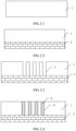
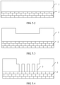
FIG. 2.1 toFIG. 2.6 are a processing flowchart of producing a metal enclosure with a structure shown inFIG. 2 ; -
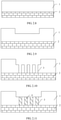
FIG. 2.7 to FIG. 2.13 are another processing flowchart of producing a metal enclosure with a structure shown inFIG. 2 ; -
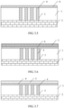
FIG. 3 is a cross sectional view of a metal enclosure in anEmbodiment 2 at a location perpendicular to a gap; -
FIG. 3.1 to FIG. 3.7 are a processing flowchart of producing a metal enclosure with a structure shown inFIG. 3 ; -
FIG. 4 is a cross sectional view of a metal enclosure in anEmbodiment 3 at a location perpendicular to a gap; -
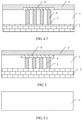
FIG. 4.1 to FIG. 4.7 are a processing flowchart of producing a metal enclosure with a structure shown inFIG. 4 ; -
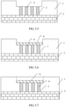
FIG. 5 is a cross sectional view of a metal enclosure in anEmbodiment 4 at a location perpendicular to a gap where theembodiment 4 embodies the technical teaching ofclaim 1; and -
FIG. 5.1 to FIG. 5.8 are a processing flowchart of producing a metal enclosure with a structure shown inFIG. 5 . - 1: Housing; 2: Plastic reinforcement layer; 3: Gap; 4: Insulation object; 5: Insulation film; 6: Reflective film; 7: Metal film
- Although hereinafter, several "embodiments" of the invention are listed, it should be understood that
claim 1 is embodied in particular with theembodiment 4 as described below but some steps and features used in theembodiment 4 are also used in the other embodiments to which the invention is not directly related. - As shown in
FIG. 1 and FIG. 2, FIG. 1 is a diagram of an integrated appearance of a metal enclosure provided in this embodiment, andFIG. 2 is a cross sectional view ofFIG. 1 at A-A. -
Embodiment 1 provides a metal enclosure. The metal enclosure includes ahousing 1. At least onegap 3 is provided on thehousing 1, the at least onegap 3 divides thehousing 1 into at least two electrically insulated parts, and eachgap 3 is filled with aninsulation object 4. The metal enclosure further includes aninsulation film 5 attached to a surface of thehousing 1. - An integrated metal enclosure generates electromagnetic shielding, electromagnetic wave transmission is blocked, and a communications function of an electronic device is accordingly affected. Therefore, in the foregoing embodiment, the
gap 3 is provided on thehousing 1, thegap 3 divides thehousing 1 into the at least two electrically insulated parts, each gap is filled with theinsulation object 4, and the divided parts of thehousing 1 are spliced into a whole by using theinsulation object 4. In a specific embodiment, theinsulation object 4 can be epoxy resin, a silicone sealant, or the like. In this way, thegap 3 and theinsulation object 4 form a partition on thehousing 1, so that impact exerted on electromagnetic wave transmission by electromagnetic shielding generated by thehousing 1 is avoided, and a communications function of a mobile device is ensured. A width of thegap 3 can fall, according to the embodiment claimed withclaim 3, within a range from 0.01 mm to 2.0 mm, such as 0.01 mm, 0.05 mm, 0.1 mm, 0.3 mm, 0.5 mm, 1.0 mm, or 2.0 mm. In addition, in a specific disposition, thegap 3 is specifically provided in a manner shown inFIG. 1 . A length direction of thegap 3 is perpendicular to a length direction of thehousing 1. That is, thegap 3 is horizontally arranged on thehousing 1. - In addition, the
insulation film 5 is further attached to the surface of thehousing 1, and a thickness of theinsulation film 5 can fall, according to the embodiment claimed withclaim 4, within a range from 0.003 mm to 0.1 mm, such as 0.01 mm, 0.03 mm, 0.05 mm, or 0.08 mm. Theinsulation film 5 enables the partition that is on thehousing 1 and that is formed by thegap 3 and theinsulation object 4 to be invisible in appearance, so that the metal enclosure has an integrated appearance. In a specific embodiment, theinsulation film 5 can be a metal oxide film. The metal oxide film enables the metal enclosure to have metallic luster while ensuring that the metal enclosure has an integrated appearance, so that texture of the metal enclosure is improved. - According to the invention, the metal enclosure includes a
housing 1. Aplastic reinforcement layer 2 is fastened to a cavity of thehousing 1. Fourgaps 3 may be provided on a surface of thehousing 1, a width of thegap 3 may be 0.05 mm, and a spacing between the gaps may be 0.8 mm. Each gap is filled with aninsulation object 4 such as epoxy resin or a silicone sealant. In addition, aninsulation film 5 is further attached to the surface of thehousing 1, and a thickness of theinsulation film 5 can be 0.02 mm. Because of limitation of a production technology, there may be an error of 0.01 mm for the thickness of theinsulation film 5, and therefore, the thickness of theinsulation film 5 may range from 0.02-0.01 mm to 0.02+0.01 mm. During production of the metal enclosure in the foregoing embodiment, the following steps are included. - Step 1: As shown in
FIG. 2.1 , produce ahousing 1 by using a metal formation technology such as die casting, stamping, forging, or CNC computer numerical control machining. - Step 2: As shown in
FIG. 2.2 , form aplastic reinforcement layer 2 in a cavity of thehousing 1 by using a metal-plastic combination technology such as nano injection molding, in-film injection molding, glue adhering, hot melting, or ultrasonic welding. Theplastic reinforcement layer 2 increases strength of thehousing 1, and further improves a cavity structure of thehousing 1. - Step 3: As shown in
FIG. 2.3 , cut thehousing 1 to form at least onegap 3. The at least onegap 3 divides thehousing 1 into at least two electrically insulated parts. Specifically, thehousing 1 is cut to form fourgaps 3 whose widths are 0.05 mm, a spacing between thegaps 3 is 0.8 mm, and the fourgaps 3 are arranged on thehousing 1 in parallel. - Step 4: As shown in
FIG. 2.4 , fill eachgap 3 with aninsulation object 4. Specifically, eachgap 3 may be filled with theinsulation object 4 such as epoxy resin or a silicone sealant, and after theinsulation object 4 is solidified, a surface of thehousing 1 may be smoothed, polished, and cleaned. In this way, thegaps 3 and theinsulation object 4 form four partitions on thehousing 1, so that impact exerted on electromagnetic wave transmission by electromagnetic shielding generated by thehousing 1 is avoided. - Step 5: As shown in
FIG. 2.5 and FIG. 2.6 , form aninsulation film 5 on the surface of thehousing 1. Specifically, aninsulation film 5 whose thickness may be 0.02+/-0.01 mm is formed on the surface of thehousing 1. Theinsulation film 5 enables the four partitions on thehousing 1 that are formed by thegaps 3 and theinsulation object 4 to be invisible in appearance, so that the metal enclosure has an integrated appearance. - During specific production of the
insulation film 5, as shown inFIG. 2.5 , ametal film 7 is first formed on the surface of thehousing 1, and a thickness of themetal film 7 may be 0.02+/-0.005 mm; and then, as shown inFIG. 2.6 , themetal film 7 is converted into a metal oxide film by means of anodic oxidation. In an anodic oxidation process, a color of an obtained metal oxide film layer may further be adjusted by means of electrolytic coloring. The metal oxide film enables the metal enclosure to have metallic luster while ensuring that the metal enclosure has an integrated appearance. In addition, coloring may be performed as needed, so that texture of the metal enclosure is improved. - In a specific embodiment, an aluminum film may be plated on the surface of the
housing 1 usually by using a technology such as PVD (physical vapor deposition), CVD (chemical vapor deposition), ion plating, physical ejecting, or electroplating, and aluminum is converted into aluminum oxide by means of anodic oxidation, and is attached to the surface of thehousing 1. The aluminum oxide has advantages such as high hardness and fine abrasion resistance, so that the texture of the metal enclosure is improved. - Alternatively, the metal enclosure in the foregoing embodiment may be produced by using the following production method, and the following steps are specifically included.
- Step 1: As shown in
FIG. 2.7 , produce ahousing 1 by using a metal formation technology such as die casting, stamping, forging, or CNC computer numerical control machining. - Step 2: As shown in
FIG. 2.8 , form aplastic reinforcement layer 2 in a cavity of thehousing 1 by using a metal-plastic combination technology such as nano injection molding, in-film injection molding, glue adhering, hot melting, or ultrasonic welding, and theplastic reinforcement layer 2 increases strength of thehousing 1, and further improves a cavity structure of thehousing 1. - Step 3: As shown in
FIG. 2.9 , provide a groove on a surface of thehousing 1. Specifically, the groove is provided on the surface of thehousing 1, a width of the groove matches a width, a spacing, and a quantity of agap 3 provided instep 4, and a depth of the groove matches a thickness of filler disposed instep 6. This is the same as in theembodiment 4 relating to the embodiment of the present invention as claimed. The width of the groove may be 2.6 mm, and the depth of the groove may be 0.02 mm. - Step 4: As shown in
FIG. 2.10 , cut a bottom wall of the groove to form at least onegap 3. The at least onegap 3 divides thehousing 1 into at least two electrically insulated parts. Specifically, the bottom wall of the groove is cut to form fourgaps 3 whose widths may be 0.05 mm, a spacing between thegaps 3 may be 0.8 mm, and the fourgaps 3 are arranged in parallel. - Step 5: As shown in
FIG. 2.11 , fill eachgap 3 with aninsulation object 4. Specifically, eachgap 3 is filled with theinsulation object 4 such as epoxy resin or a silicone sealant, and after theinsulation object 4 is solidified, the surface of thehousing 1 is smoothed, polished, and cleaned. In this way, thegaps 3 and theinsulation object 4 form four partitions on thehousing 1, so that impact exerted on electromagnetic wave transmission by electromagnetic shielding generated by thehousing 1 is avoided. - Step 6: As shown in
FIG. 2.12 , deposit, in the groove, filler of a same material as thehousing 1. A cavity of the groove is filled with the filler as inembodiment 4 relating to the embodiment of the present invention as claimed. Thehousing 1 may be made of an aluminum material, and an aluminum layer is deposited in the groove by using a technology such as PVD, CVD, ion plating, physical ejecting, or electroplating. - Step 7: As shown in
FIG. 2.13 , form aninsulation film 5 on the surface of thehousing 1. Specifically, anodic oxidation processing is performed on thehousing 1, to form a metal oxide film on the surface of thehousing 1. In an anodic oxidation process, a color of an obtained metal oxide film layer may further be adjusted by means of electrolytic coloring. The metal oxide film enables the metal enclosure to have metallic luster while ensuring that the metal enclosure has an integrated appearance. In addition, coloring may be performed as needed, so that texture of the metal enclosure is improved. - When the
housing 1 is made of an aluminum material, an aluminum oxide film is formed on the surface of thehousing 1 by using an anodic oxidation technology. Aluminum oxide has advantages such as high hardness and fine abrasion resistance, so that the texture of the metal enclosure is improved. - As shown in
FIG. 3, FIG. 3 is a cross sectional view of a metal enclosure provided in this embodiment at a location perpendicular to a gap. - This embodiment provides a metal enclosure. The metal enclosure includes the
housing 1, thegap 3, theinsulation object 4, and theinsulation film 5 inEmbodiment 1, all the foregoing structures are the same as the structures and the dispositions inEmbodiment 1, and details are not described herein again. A difference between the metal enclosure provided in this embodiment and the metal enclosure inEmbodiment 1 is that the metal enclosure provided in this embodiment further includes areflective film 6. Thereflective film 6 is specifically disposed between thehousing 1 and theinsulation film 5, and covers an entire surface of thehousing 1. - The
reflective film 6 may provide a reflective rate approximate to that of metal of thehousing 1, so that a partition that is on the surface of thehousing 1 and that is formed by thegap 3 and theinsulation object 4 has no obvious brightness difference in appearance from thehousing 1. Specifically, thereflective film 6 may be an imitated metal coating, or thereflective film 6 may be made from indium, tin, or an indium-tin alloy by means of deposition. - In a specific embodiment, the metal enclosure includes a
housing 1. Aplastic reinforcement layer 2 is fastened to a cavity of the housing 1as inembodiment 4 relating to the embodiment of the present invention as claimed. Fourgaps 3 are provided on a surface of thehousing 1, a width of thegap 3 may be 0.1 mm, and a spacing between the gaps may be 0.8 mm. Each gap may be filled with aninsulation object 4 such as epoxy resin or a silicone sealant. Aninsulation film 5 is further attached to the surface of thehousing 1, and a thickness of theinsulation film 5 is 0.03 mm. Because of limitation of a production technology, there may be an error of 0.01 mm for the thickness of theinsulation film 5, and therefore, the thickness of theinsulation film 5 may range from 0.03-0.01 mm to 0.03+0.01 mm. In addition, areflective film 6 is further included, thereflective film 6 is between thehousing 1 and theinsulation film 5, and thereflective film 6 covers the entire surface of thehousing 1. During production of the metal enclosure in the foregoing embodiment, the following steps are included. - As shown in
FIG. 3.1 to FIG. 3.4 ,step 1,step 2,step 3, andstep 4 in a production method provided in this embodiment is the same asstep 1,step 2,step 3, andstep 4 inEmbodiment 1 shown inFIG. 2.1 to FIG. 2.4 , and details are not described herein again. The production method provided in this embodiment further includes the following steps. - Step 5: As shown in
FIG. 3.5 , form areflective film 6 on the surface of thehousing 1. Specifically, areflective film 6 with a thickness at a nanometer level is formed on the surface of thehousing 1, and thereflective film 6 covers the entire surface of thehousing 1. Thereflective film 6 may provide a reflective rate approximate to that of metal of thehousing 1, so that the four partitions on thehousing 1 that are formed by thegaps 3 and theinsulation object 4 have no obvious brightness difference in appearance from thehousing 1. Specifically, thereflective film 6 is an imitated metal coating, or thereflective film 6 may be made from indium, tin, or an indium-tin alloy by means of deposition. - Step 6: As shown in
FIG. 3.6 and FIG. 3.7 , form aninsulation film 5 on the surface of thehousing 1. Specifically, aninsulation film 5 whose thickness may be 0.03+/-0.01 mm is formed on thereflective film 6. Theinsulation film 5 enables the four partitions on thehousing 1 that are formed by thegaps 3 and theinsulation object 4 to be invisible in appearance, so that the metal enclosure has an integrated appearance. - During specific production of the
insulation film 5, as shown inFIG. 3.6 , ametal film 7 is first formed on a surface of thereflective film 6, and a thickness of themetal film 7 may be 0.03+/-0.005 mm; and then, as shown inFIG. 3.7 , themetal film 7 is converted into a metal oxide film by means of anodic oxidation. In an anodic oxidation process, a color of an obtained metal oxide film layer may be adjusted by means of electrolytic coloring. The metal oxide film enables the metal enclosure to have metallic luster while ensuring that the metal enclosure has an integrated appearance. In addition, coloring may be performed as needed, so that texture of the metal enclosure is improved. - In a specific embodiment, an aluminum oxide film may be formed on the surface of the
housing 1. A specific production method is the same as the method used for producing the aluminum oxide film inEmbodiment 1, and details are not described herein again. The aluminum oxide has advantages such as high hardness and fine abrasion resistance, so that the texture of the metal enclosure is improved. - As shown in
FIG. 4, FIG. 4 is a cross sectional view of a metal enclosure provided in this embodiment at a location perpendicular to a gap. - This embodiment provides a metal enclosure. A difference between the metal enclosure and the metal enclosure in
Embodiment 2 lies only in that areflective film 6 is disposed at a different location, other structures are the same, and details are not described herein again. In this embodiment, thereflective film 6 is between ahousing 1 and aninsulation film 5, and thereflective film 6 covers a surface of at least onegap 3. When two ormore gaps 3 are formed on thehousing 1 by means of cutting, thereflective film 6 further covers an area betweenneighboring gaps 3 in the two ormore gaps 3. - In addition, the
reflective film 6 provided in this embodiment has a same effect as thereflective film 6 inEmbodiment 2, and both may provide a reflective rate approximate to that of metal of thehousing 1, so that partitions on a surface of thehousing 1 that are formed by thegaps 3 and theinsulation object 4 have no obvious brightness difference in appearance from thehousing 1. Specifically, thereflective film 6 may be an imitated metal coating, or thereflective film 6 may be made from indium, tin, or an indium-tin alloy by means of deposition. - In a specific embodiment, the metal enclosure includes a
housing 1. Aplastic reinforcement layer 2 is fastened to a cavity of thehousing 1. Fourgaps 3 are provided on a surface of thehousing 1, a width of thegap 3 may be 0.2 mm, and a spacing between the gaps may be 0.8 mm. Each gap is filled with aninsulation object 4 such as epoxy resin or a silicone sealant. Aninsulation film 5 is further attached to the surface of thehousing 1, and a thickness of theinsulation film 5 may be 0.04 mm. Because of limitation of a production technology, there is an error of 0.01 mm for the thickness of theinsulation film 5, and therefore, the thickness of theinsulation film 5 ranges from 0.04-0.01 mm to 0.04+0.01 mm. In addition, areflective film 6 is further included, thereflective film 6 is between thehousing 1 and theinsulation film 5, and thereflective film 6 covers surfaces of the fourgaps 3 and covers an area betweenneighboring gaps 3 in the fourgaps 3. During production of the metal enclosure in the foregoing embodiment, the following steps are included. - As shown in
FIG. 4.1 to FIG. 4.4 ,step 1,step 2,step 3, andstep 4 in a production method provided in this embodiment is the same asstep 1,step 2,step 3, andstep 4 inEmbodiment 1 shown inFIG. 2.1 to FIG. 2.4 , and details are not described herein again. The production method provided in this embodiment further includes the following steps. - Step 5: As shown in
FIG. 4.5 , form areflective film 6 on the surface of thehousing 1. Specifically, areflective film 6 with a thickness at a nanometer level is formed on the surface of thehousing 1, and thereflective film 6 covers surfaces of the fourgaps 3 and an area betweenneighboring gaps 3 in the fourgaps 3. Thereflective film 6 may provide a reflective rate approximate to that of metal of thehousing 1, so that the four partitions on thehousing 1 that are formed by thegaps 3 and theinsulation object 4 have no obvious brightness difference in appearance from thehousing 1. Specifically, thereflective film 6 may be an imitated metal coating, or thereflective film 6 may be made from indium, tin, or an indium-tin alloy by means of deposition. - Step 6: As shown in
FIG. 4.6 andFIG. 4.7 , form aninsulation film 5 on the surface of thehousing 1. Specifically, aninsulation film 5 whose thickness may be 0.04+/-0.01 mm is formed on the surface of thehousing 1, and theinsulation film 5 covers an entire surface area of thehousing 1. Theinsulation film 5 enables the four partitions on thehousing 1 that are formed by thegaps 3 and theinsulation object 4 to be invisible in appearance, so that the metal enclosure has an integrated appearance. - During the specific production of the
insulation film 5, as shown inFIG. 4.6 , ametal film 7 is first formed on the surface of thehousing 1 and a surface of thereflective film 6, and a thickness of themetal film 7 may be 0.04+/-0.005 mm; and then, as shown inFIG. 4.7 , themetal film 7 is converted into a metal oxide film by means of anodic oxidation. In an anodic oxidation process, a color of an obtained metal oxide film layer may be adjusted by means of electrolytic coloring. The metal oxide film enables the metal enclosure to have metallic luster while ensuring that the metal enclosure has an integrated appearance. In addition, coloring may be performed as needed, so that texture of the metal enclosure is improved. - In a specific embodiment, an aluminum oxide film may be formed on the surface of the
housing 1. A specific production manner is the same as the method used for producing the aluminum oxide film inEmbodiment 1, and details are not described herein again. The aluminum oxide has advantages such as high hardness and fine abrasion resistance, so that the texture of the metal enclosure is improved. - As explained above,
Embodiment 4 is the embodiment of the present invention as claimed. As shown inFIG. 5, FIG. 5 is a cross sectional view of a metal enclosure provided in this embodiment of the present invention at a location perpendicular to a gap. - This embodiment of the present invention provides a metal enclosure. A difference between the metal enclosure and the metal enclosure in
Embodiment 3 lies only in that a groove is further provided on an area at which agap 3 is provided. According to the invention inclaim 1, areflective film 6 is disposed in the groove, that is, the groove is provided on a surface of ahousing 1, thegap 3 is provided on a bottom wall of the groove, and thereflective film 6 covering the bottom wall of the groove is further in the groove. - In addition, the
reflective film 6 provided in this embodiment has a same effect as thereflective film 6 inEmbodiment 3, and both may provide a reflective rate approximate to that of metal of thehousing 1, so that a partition that is on the surface of the housing and that is formed by thegap 3 and theinsulation object 4 has no obvious brightness difference in appearance from thehousing 1. Specifically, thereflective film 6 may be, as claimed with the embodiment ofclaim 2, an imitated metal coating, or thereflective film 6 may be made, as claimed with the embodiment ofclaim 7, from indium, tin, or an indium-tin alloy by means of deposition. - In this
embodiment 4 relating to the embodiment of the present invention as claimed, the metal enclosure includes ahousing 1. Aplastic reinforcement layer 2 is fastened to a cavity of thehousing 1. Fourgaps 3 are provided on the surface of thehousing 1, a width of thegap 3 may be 0.3 mm, and a spacing between the gaps may be 0.8 mm. Each gap is filled with aninsulation object 4 such as epoxy resin or a silicone sealant. Aninsulation film 5 is further attached to the surface of thehousing 1, and a thickness of theinsulation film 5 may be 0.05 mm. Because of limitation of a production technology, there may be an error of 0.01 mm for the thickness of theinsulation film 5, and therefore, the thickness of theinsulation film 5 ranges from 0.05-0.01 mm to 0.05+0.01 mm. According to the invention claimed inclaim 1, a groove on the surface of thehousing 1 is further included, thegap 3 is provided on a bottom wall of the groove, and areflective film 6 covering the bottom wall of the groove is further in the groove. During production of the metal enclosure in the foregoing embodiment, the following steps are included. - Step 1: As shown in
FIG. 5.1 , produce ahousing 1 by using a metal formation technology such as die casting, stamping, forging, or CNC computer numerical control machining. - Step 2: As shown in
FIG. 5.2 , form aplastic reinforcement layer 2 in a cavity of thehousing 1 by using a metal-plastic combination technology such as nano injection molding, in-film injection molding, glue adhering, hot melting, or ultrasonic welding. Theplastic reinforcement layer 2 increases strength of thehousing 1, and further improves a cavity structure of thehousing 1. - Step 3: As shown in
FIG. 5.3 , provide a groove on a surface of thehousing 1. Specifically, according to the invention as claimed inclaium 1, the groove is provided on the surface of thehousing 1, a width of the groove matches a width, a spacing, and a quantity of a gap disposed instep 4, and a depth of the groove matches a thickness of filler disposed instep 7. In this embodiment, the width of the groove is 3.6 mm, and the depth of the groove is 0.05 mm. - Step 4: As shown in
FIG. 5.4 , cut a bottom wall of the groove to form at least onegap 3. The at least onegap 3 divides thehousing 1 into at least two electrically insulated parts. Specifically, the bottom wall of the groove is cut to form fourgaps 3 whose widths are 0.3 mm, a spacing between the gaps is 0.8 mm, and the fourgaps 3 are arranged in parallel. - Step 5: As shown in
FIG. 5.5 , fill eachgap 3 with aninsulation object 4. Specifically, eachgap 3 is filled with theinsulation object 4 such as epoxy resin or a silicone sealant, and after theinsulation object 4 is solidified, the surface of thehousing 1 is smoothed, polished, and cleaned. Thegaps 3 and theinsulation object 4 form four partitions on thehousing 1, so that impact exerted on electromagnetic wave transmission by electromagnetic shielding generated by thehousing 1 is avoided. - Step 6: As shown in
FIG. 5.6 , according to the present invention, lay areflective film 6 in the groove. Specifically, areflective film 6 with a thickness at a nanometer level is disposed in the groove, and according to the present invention, thereflective film 6 covers the bottom wall of the groove. Thereflective film 6 may provide a reflective rate approximate to that of metal of thehousing 1, so that thegaps 3 have no obvious brightness difference in appearance. Specifically, thereflective film 6 as claimed inclaim 6 is an imitated metal coating, or thereflective film 6 as claimed inclaim 7 is made from indium, tin, or an indium-tin alloy by means of deposition. - Step 7: As shown in
FIG. 5.7 , according to the invention, deposit, in the groove, a filler of a same material as thehousing 1. A cavity of the groove is filled with the filler. In a specific embodiment, thehousing 1 is made of an aluminum material, and an aluminum layer is deposited in the groove by using a technology such as PVD, CVD, ion plating, physical ejecting, or electroplating. - Step 8: As shown in
FIG. 5.8 , form aninsulation film 5 on the surface of thehousing 1. Specifically, anodic oxidation processing is performed on thehousing 1, to form a metal oxide film on the surface of thehousing 1. In an anodic oxidation process, a color of an obtained metal oxide film layer may be adjusted by means of electrolytic coloring. The metal oxide film enables the metal enclosure to have metallic luster while ensuring that the metal enclosure has an integrated appearance. In addition, coloring may be performed as needed, so that texture of the metal enclosure is improved. - When the
housing 1 is made by using an aluminum material, an aluminum oxide film is formed on the surface of thehousing 1 by means of anodic oxidation. Aluminum oxide has advantages such as high hardness and fine abrasion resistance, so that the texture of the metal enclosure is improved. - It can be learned from the foregoing description that the metal enclosures provided in
Embodiment 1 to Embodiment 4 (which is the embodiment of the present invention) include ahousing 1. Agap 3 is provided on thehousing 1, thegap 3 divides thehousing 1 into at least two electrically insulated parts, eachgap 3 is filled with aninsulation object 4, and the divided parts of thehousing 1 are spliced into a whole by using theinsulation object 4. In this way, thegap 3 and theinsulation object 4 form a partition on thehousing 1, so that impact exerted on electromagnetic wave transmission by electromagnetic shielding generated by thehousing 1 is avoided. Aninsulation film 5 is further attached to a surface of thehousing 1, and theinsulation film 5 enables the partition formed by thegap 3 and theinsulation object 4 to be invisible in appearance, so that the metal enclosure has an integrated appearance. - The embodiments further provide a production method for the metal enclosure in the foregoing embodiment, and the following steps are included.
- Cut a
housing 1 to form at least onegap 3. The at least onegap 3 divides thehousing 1 into at least two electrically insulated parts. - Fill each
gap 3 with aninsulation object 4. - Form an
insulation film 5 on a surface of thehousing 1. - To enable the metal enclosure to have an integrated appearance and have metallic luster, a metal oxide film may be specifically formed on the surface of the
housing 1. A metal enclosure with the structure shown inFIG. 2 is produced by using the two production methods inEmbodiment 1. To improve texture of the metal enclosure, areflective film 6 may be further laid between thehousing 1 and theinsulation film 5, and thereflective film 6, according to the embodiment claimed withclaim 5, covers the entire surface of thehousing 1. A metal enclosure with the structure inFIG. 3 is produced by using the production method inEmbodiment 2. In addition, alternatively, thereflective film 6 may cover only an area that is on thehousing 1 and at which the at least onegap 3 is formed by means of cutting. Specifically, thereflective film 6 covers a surface of the at least onegap 3, and when two ormore gaps 3 are formed on thehousing 1 by means of cutting, thereflective film 6 further covers an area betweenneighboring gaps 3 in the two ormore gaps 3. A metal enclosure with the structure inFIG. 4 is produced by using the method inEmbodiment 3. - According to the invention as claimed in
claim 1, a groove is provided on the surface of thehousing 1, the at least onegap 3 is provided on a bottom wall of the groove, and areflective film 6 is laid on the bottom wall of the groove. A metal enclosure with the structure inFIG. 5 is produced by using the production method inEmbodiment 4 of the invention. - The present invention further provides, according to the invention in claim 8, a mobile device. The mobile device includes a device body and the metal enclosure according to
Embodiment 4 that is fixedly connected to the device body, and further includes an antenna disposed on the device body. At least one of at least two electrically insulated parts in the metal enclosure is used as a radiating element of the antenna. For the metal enclosure of the mobile device, agap 3 is provided on ahousing 1, thegap 3 divides thehousing 1 into at least two electrically insulated parts, and eachgap 3 is filled with aninsulation object 4. In this way, thegap 3 and theinsulation object 4 form a partition on thehousing 1, so that impact exerted on electromagnetic wave transmission by electromagnetic shielding generated by thehousing 1 is avoided. Aninsulation film 5 is further attached to a surface of thehousing 1, and theinsulation film 5 enables the partition formed by thegap 3 and theinsulation object 4 to be invisible in appearance, so that the metal enclosure has an integrated appearance.
Claims (8)
- A metal enclosure of a mobile device, wherein the metal enclosure comprises a housing (1) having a first side and a second side opposite the first side and a plastic reinforcement layer (2) fastened to a cavity of the housing (1) at the second side, wherein at least one gap (3) is provided on the housing (1), the at least one gap (3) divides the housing (1) into at least two electrically insulated parts, and each gap (3) is filled with an insulation object (4); and further comprising an insulation film (5) attached to a surface at the first side of the housing (1); further comprising
a groove located on the surface at the first side of the housing (1), wherein the at least one gap (3) is provided on a bottom wall of the groove, and a reflective film (6) covering the bottom wall of the groove is further disposed in the groove, wherein a width of the groove matches a width, a spacing, and a quantity of the at least one gap, and a depth of the groove matches a thickness of a filler disposed in the groove between the reflective film (6) and the surface at the first side. - The metal enclosure of a mobile device according to claim 1, wherein the insulation film (5) is a metal oxide film.
- The metal enclosure of a mobile device according to claim 1, wherein a width of each gap (3) falls within a range from 0.01 mm to 2.0 mm.
- The metal enclosure of a mobile device according to claim 1, wherein a thickness of the insulation film (5) falls within a range from 0.003 mm to 0.10 mm.
- The metal enclosure of a mobile device according to claim 1, further comprising a reflective film (6) between the housing (1) and the insulation film (5), wherein the reflective film (6) is configured to cover the entire surface of the housing (1).
- The metal enclosure of a mobile device according to claim 5, wherein the reflective film (6) is an imitated metal coating.
- The metal enclosure of a mobile device according to claim 5, wherein the reflective film (6) is made from indium, tin, or an indium-tin alloy by means of deposition.
- A mobile device, comprising a device body and the metal enclosure according to any one of claims 1 to 7 that is fixedly connected to the device body, and further comprising an antenna disposed on the device body, wherein at least one of at least two electrically insulated parts in the metal enclosure is used as a radiating element of the antenna.
Applications Claiming Priority (2)
| Application Number | Priority Date | Filing Date | Title |
|---|---|---|---|
| CN201610867934.4A CN107872936B (en) | 2016-09-28 | 2016-09-28 | Metal shell of mobile device, preparation method of metal shell and mobile device |
| PCT/CN2017/086631 WO2018058995A1 (en) | 2016-09-28 | 2017-05-31 | Metal housing of mobile device and manufacturing method therefor, and mobile device |
Publications (3)
| Publication Number | Publication Date |
|---|---|
| EP3493660A1 EP3493660A1 (en) | 2019-06-05 |
| EP3493660A4 EP3493660A4 (en) | 2019-07-10 |
| EP3493660B1 true EP3493660B1 (en) | 2022-01-26 |
Family
ID=61761956
Family Applications (1)
| Application Number | Title | Priority Date | Filing Date |
|---|---|---|---|
| EP17854451.6A Active EP3493660B1 (en) | 2016-09-28 | 2017-05-31 | Metal housing of mobile device and manufacturing method therefor, and mobile device |
Country Status (6)
| Country | Link |
|---|---|
| US (1) | US11178785B2 (en) |
| EP (1) | EP3493660B1 (en) |
| JP (1) | JP2019537238A (en) |
| KR (1) | KR102282120B1 (en) |
| CN (1) | CN107872936B (en) |
| WO (1) | WO2018058995A1 (en) |
Families Citing this family (9)
| Publication number | Priority date | Publication date | Assignee | Title |
|---|---|---|---|---|
| CN110444855B (en) * | 2018-05-02 | 2021-03-02 | 惠州硕贝德无线科技股份有限公司 | Dual-polarized 5G antenna integrated on metal frame of mobile terminal |
| CN110662379B (en) * | 2018-06-28 | 2022-02-18 | 华为机器有限公司 | Shell of terminal |
| CN110650605A (en) * | 2019-09-18 | 2020-01-03 | Oppo广东移动通信有限公司 | Shell assembly, preparation method thereof and electronic equipment |
| KR102612938B1 (en) * | 2019-10-23 | 2023-12-12 | 삼성전자 주식회사 | Electronic device including antenna module |
| CN114554739B (en) * | 2020-11-25 | 2025-07-25 | 华为技术有限公司 | Shell, electronic equipment and shell manufacturing method |
| KR20220077611A (en) * | 2020-12-02 | 2022-06-09 | 삼성전자주식회사 | Electronic device including housing |
| CN114976586A (en) * | 2021-02-25 | 2022-08-30 | 北京小米移动软件有限公司 | Frame body of communication terminal and communication terminal |
| TWI765743B (en) * | 2021-06-11 | 2022-05-21 | 啓碁科技股份有限公司 | Antenna structure |
| CN117319534A (en) * | 2023-09-07 | 2023-12-29 | 深圳市零壹创新科技有限公司 | A protective case for electronic equipment |
Family Cites Families (25)
| Publication number | Priority date | Publication date | Assignee | Title |
|---|---|---|---|---|
| JP3869255B2 (en) * | 2001-06-14 | 2007-01-17 | 富士通株式会社 | Metal molded body manufacturing method and metal molded body manufactured thereby |
| DE602006015290D1 (en) | 2006-05-19 | 2010-08-19 | Amc Centurion Ab | Metal housing with slotted antennas for radio communication device |
| US7886437B2 (en) * | 2007-05-25 | 2011-02-15 | Electro Scientific Industries, Inc. | Process for forming an isolated electrically conductive contact through a metal package |
| JP5017207B2 (en) * | 2007-09-18 | 2012-09-05 | 信越ポリマー株式会社 | Radio wave transmitting decorative member |
| JP5314300B2 (en) * | 2008-03-12 | 2013-10-16 | シチズン時計株式会社 | Decorative material |
| CN101888754A (en) * | 2009-05-14 | 2010-11-17 | 富准精密工业(深圳)有限公司 | Shell and manufacturing method thereof |
| FR2957749A1 (en) * | 2010-03-22 | 2011-09-23 | Sorin Crm Sas | METHOD FOR PRODUCING AN ELECTRICAL CROSSROAD IN THE METAL WALL OF A HOUSING, IN PARTICULAR AN ACTIVE MEDICAL DEVICE, AND DEVICE COMPRISING SUCH A TRAVERSEE |
| US9413861B2 (en) * | 2012-10-05 | 2016-08-09 | Nokia Technologies Oy | Metallization and anodization of plastic and conductive parts of the body of an apparatus |
| US9655261B2 (en) * | 2013-03-21 | 2017-05-16 | Htc Corporation | Casing of electronic device and method of manufacturing the same |
| US9209513B2 (en) * | 2013-06-07 | 2015-12-08 | Apple Inc. | Antenna window and antenna pattern for electronic devices and methods of manufacturing the same |
| CN104377424A (en) | 2013-08-14 | 2015-02-25 | 三星电机株式会社 | Cover for electronic device, antenna assembly, electronic device, and method for manufacturing the same |
| CN104735942A (en) * | 2013-12-20 | 2015-06-24 | 惠州比亚迪电子有限公司 | Communication equipment metal shell and manufacturing method thereof |
| CN104735941B (en) * | 2013-12-20 | 2019-01-11 | 比亚迪股份有限公司 | A kind of communication apparatus metal shell and preparation method thereof |
| US9264090B2 (en) * | 2014-01-07 | 2016-02-16 | Otter Products, Llc | Metallic protective case for electronic device |
| CN104168730B (en) * | 2014-02-26 | 2019-06-11 | 深圳富泰宏精密工业有限公司 | Shell, using electronic device of the shell and preparation method thereof |
| CA2953629C (en) * | 2014-03-28 | 2021-10-26 | Huawei Device Co., Ltd. | Integrated structure of metal housing and antenna of electronic apparatus |
| CN105282998B (en) * | 2014-05-30 | 2019-07-26 | 光宝电子(广州)有限公司 | The shell of electronic equipment and electronic equipment including the shell |
| CN105530786A (en) * | 2014-12-26 | 2016-04-27 | 比亚迪股份有限公司 | Communication equipment metal case and preparation method thereof |
| CN105530791B (en) | 2014-12-26 | 2016-10-12 | 比亚迪股份有限公司 | A kind of electronic product metal shell being formed with antenna slot and preparation method thereof |
| CN105530783B (en) * | 2014-12-26 | 2016-10-12 | 比亚迪股份有限公司 | A kind of communication apparatus metal shell and preparation method thereof |
| CN105530788A (en) | 2014-12-26 | 2016-04-27 | 比亚迪股份有限公司 | Communication equipment metal case and preparation method thereof |
| CN105744015A (en) * | 2014-12-26 | 2016-07-06 | 小米科技有限责任公司 | Electronic communication device with metal shell and processing method of metal shell |
| CN105517389A (en) * | 2016-01-08 | 2016-04-20 | 广东欧珀移动通信有限公司 | Mobile terminal casing and processing method thereof |
| CN105960131A (en) * | 2016-06-23 | 2016-09-21 | 东莞劲胜精密组件股份有限公司 | 3C electronic product shell and preparation method thereof |
| US10321590B2 (en) * | 2016-09-06 | 2019-06-11 | Apple Inc. | Interlock features of a portable electronic device |
-
2016
- 2016-09-28 CN CN201610867934.4A patent/CN107872936B/en active Active
-
2017
- 2017-05-31 JP JP2019510611A patent/JP2019537238A/en active Pending
- 2017-05-31 KR KR1020197007479A patent/KR102282120B1/en active Active
- 2017-05-31 WO PCT/CN2017/086631 patent/WO2018058995A1/en not_active Ceased
- 2017-05-31 EP EP17854451.6A patent/EP3493660B1/en active Active
-
2019
- 2019-03-27 US US16/366,726 patent/US11178785B2/en active Active
Non-Patent Citations (1)
| Title |
|---|
| None * |
Also Published As
| Publication number | Publication date |
|---|---|
| KR20190038655A (en) | 2019-04-08 |
| CN107872936B (en) | 2020-10-23 |
| US11178785B2 (en) | 2021-11-16 |
| KR102282120B1 (en) | 2021-07-26 |
| WO2018058995A1 (en) | 2018-04-05 |
| EP3493660A1 (en) | 2019-06-05 |
| EP3493660A4 (en) | 2019-07-10 |
| CN107872936A (en) | 2018-04-03 |
| JP2019537238A (en) | 2019-12-19 |
| US20190223311A1 (en) | 2019-07-18 |
Similar Documents
| Publication | Publication Date | Title |
|---|---|---|
| US11178785B2 (en) | Metal enclosure of mobile device, production method for metal enclosure, and mobile device | |
| CN103781296B (en) | Electronic device housing manufacture method | |
| US10862186B2 (en) | Waveguide device comprising a core having a waveguide channel, where a smoothing layer and a conductive layer of at least 5 skin depth are formed on an inner surface of the waveguide channel | |
| KR102045537B1 (en) | Deco film manufacturing method of deco film having three dimensional pattern, glass structure forming method and composite sheet structure forming method using deco film | |
| CN102039699B (en) | Metal foil laminated film and manufacture method thereof | |
| JP6665781B2 (en) | Housing parts, electronic equipment, and manufacturing method of housing parts | |
| TW202018879A (en) | Multi-layer thin-film coatings for system-in-package assemblies in portable electronic devices | |
| CN104853576A (en) | Electromagnetic shielding membrane with excellent shielding performance and production technology thereof | |
| CN106455391B (en) | 3C electronic product shell and preparation method thereof | |
| EP3451448B1 (en) | Insulator, metallic shell, method for manufacturing the same and mobile terminal having the same | |
| CN106211684B (en) | Shell, using electronic device of the shell and preparation method thereof | |
| KR20190028704A (en) | Electrical connection for electro-optical elements | |
| CN106159132A (en) | Battery cover plate, preparation method thereof, and electronic device | |
| CN104527307A (en) | Method for realizing monochromatic double-luster, plastic housing and terminal | |
| CN105813411A (en) | Housing, electronic device provided with housing, and manufacturing method thereof | |
| CN104538735A (en) | Metal outer frame antenna used for mobile terminal | |
| CN101887860A (en) | Electronic element manufacturing method and packaging structure thereof | |
| CN105862037B (en) | Stainless steel plate, preparation method and electronic equipment | |
| WO2021027063A1 (en) | Antenna structure for electronic device | |
| CN104868226A (en) | Electronic device and manufacturing method | |
| EP1401646B1 (en) | Layered structure providing shielding characteristics | |
| CN106710690A (en) | Electromagnetic shielding film for cables, manufacturing method of electromagnetic shielding film and manufacturing method of cables | |
| EP3281777B1 (en) | Cover plate, method for manufacturing cover plate and electronic device | |
| US20250219668A1 (en) | Communication apparatus and case for a communication apparatus | |
| US20150111047A1 (en) | Chemical plating product and method forming thereof |
Legal Events
| Date | Code | Title | Description |
|---|---|---|---|
| STAA | Information on the status of an ep patent application or granted ep patent |
Free format text: STATUS: THE INTERNATIONAL PUBLICATION HAS BEEN MADE |
|
| PUAI | Public reference made under article 153(3) epc to a published international application that has entered the european phase |
Free format text: ORIGINAL CODE: 0009012 |
|
| STAA | Information on the status of an ep patent application or granted ep patent |
Free format text: STATUS: REQUEST FOR EXAMINATION WAS MADE |
|
| 17P | Request for examination filed |
Effective date: 20190301 |
|
| AK | Designated contracting states |
Kind code of ref document: A1 Designated state(s): AL AT BE BG CH CY CZ DE DK EE ES FI FR GB GR HR HU IE IS IT LI LT LU LV MC MK MT NL NO PL PT RO RS SE SI SK SM TR |
|
| AX | Request for extension of the european patent |
Extension state: BA ME |
|
| A4 | Supplementary search report drawn up and despatched |
Effective date: 20190611 |
|
| RIC1 | Information provided on ipc code assigned before grant |
Ipc: H05K 5/04 20060101AFI20190604BHEP Ipc: G02B 6/00 20060101ALI20190604BHEP Ipc: H01Q 1/24 20060101ALI20190604BHEP Ipc: F21V 8/00 20060101ALI20190604BHEP Ipc: H04M 1/02 20060101ALI20190604BHEP |
|
| DAV | Request for validation of the european patent (deleted) | ||
| DAX | Request for extension of the european patent (deleted) | ||
| STAA | Information on the status of an ep patent application or granted ep patent |
Free format text: STATUS: EXAMINATION IS IN PROGRESS |
|
| 17Q | First examination report despatched |
Effective date: 20200312 |
|
| RIC1 | Information provided on ipc code assigned before grant |
Ipc: H01Q 1/52 20060101ALI20210812BHEP Ipc: G02B 6/00 20060101ALI20210812BHEP Ipc: F21V 8/00 20060101ALI20210812BHEP Ipc: H01Q 1/24 20060101ALI20210812BHEP Ipc: H04M 1/02 20060101ALI20210812BHEP Ipc: H05K 5/04 20060101AFI20210812BHEP |
|
| GRAP | Despatch of communication of intention to grant a patent |
Free format text: ORIGINAL CODE: EPIDOSNIGR1 |
|
| STAA | Information on the status of an ep patent application or granted ep patent |
Free format text: STATUS: GRANT OF PATENT IS INTENDED |
|
| INTG | Intention to grant announced |
Effective date: 20210924 |
|
| GRAS | Grant fee paid |
Free format text: ORIGINAL CODE: EPIDOSNIGR3 |
|
| GRAA | (expected) grant |
Free format text: ORIGINAL CODE: 0009210 |
|
| STAA | Information on the status of an ep patent application or granted ep patent |
Free format text: STATUS: THE PATENT HAS BEEN GRANTED |
|
| AK | Designated contracting states |
Kind code of ref document: B1 Designated state(s): AL AT BE BG CH CY CZ DE DK EE ES FI FR GB GR HR HU IE IS IT LI LT LU LV MC MK MT NL NO PL PT RO RS SE SI SK SM TR |
|
| REG | Reference to a national code |
Ref country code: GB Ref legal event code: FG4D |
|
| REG | Reference to a national code |
Ref country code: CH Ref legal event code: EP |
|
| REG | Reference to a national code |
Ref country code: AT Ref legal event code: REF Ref document number: 1466320 Country of ref document: AT Kind code of ref document: T Effective date: 20220215 |
|
| REG | Reference to a national code |
Ref country code: IE Ref legal event code: FG4D |
|
| REG | Reference to a national code |
Ref country code: DE Ref legal event code: R096 Ref document number: 602017052894 Country of ref document: DE |
|
| REG | Reference to a national code |
Ref country code: LT Ref legal event code: MG9D |
|
| REG | Reference to a national code |
Ref country code: NL Ref legal event code: MP Effective date: 20220126 |
|
| REG | Reference to a national code |
Ref country code: AT Ref legal event code: MK05 Ref document number: 1466320 Country of ref document: AT Kind code of ref document: T Effective date: 20220126 |
|
| PG25 | Lapsed in a contracting state [announced via postgrant information from national office to epo] |
Ref country code: NL Free format text: LAPSE BECAUSE OF FAILURE TO SUBMIT A TRANSLATION OF THE DESCRIPTION OR TO PAY THE FEE WITHIN THE PRESCRIBED TIME-LIMIT Effective date: 20220126 |
|
| PG25 | Lapsed in a contracting state [announced via postgrant information from national office to epo] |
Ref country code: SE Free format text: LAPSE BECAUSE OF FAILURE TO SUBMIT A TRANSLATION OF THE DESCRIPTION OR TO PAY THE FEE WITHIN THE PRESCRIBED TIME-LIMIT Effective date: 20220126 Ref country code: RS Free format text: LAPSE BECAUSE OF FAILURE TO SUBMIT A TRANSLATION OF THE DESCRIPTION OR TO PAY THE FEE WITHIN THE PRESCRIBED TIME-LIMIT Effective date: 20220126 Ref country code: PT Free format text: LAPSE BECAUSE OF FAILURE TO SUBMIT A TRANSLATION OF THE DESCRIPTION OR TO PAY THE FEE WITHIN THE PRESCRIBED TIME-LIMIT Effective date: 20220526 Ref country code: NO Free format text: LAPSE BECAUSE OF FAILURE TO SUBMIT A TRANSLATION OF THE DESCRIPTION OR TO PAY THE FEE WITHIN THE PRESCRIBED TIME-LIMIT Effective date: 20220426 Ref country code: LT Free format text: LAPSE BECAUSE OF FAILURE TO SUBMIT A TRANSLATION OF THE DESCRIPTION OR TO PAY THE FEE WITHIN THE PRESCRIBED TIME-LIMIT Effective date: 20220126 Ref country code: HR Free format text: LAPSE BECAUSE OF FAILURE TO SUBMIT A TRANSLATION OF THE DESCRIPTION OR TO PAY THE FEE WITHIN THE PRESCRIBED TIME-LIMIT Effective date: 20220126 Ref country code: ES Free format text: LAPSE BECAUSE OF FAILURE TO SUBMIT A TRANSLATION OF THE DESCRIPTION OR TO PAY THE FEE WITHIN THE PRESCRIBED TIME-LIMIT Effective date: 20220126 Ref country code: BG Free format text: LAPSE BECAUSE OF FAILURE TO SUBMIT A TRANSLATION OF THE DESCRIPTION OR TO PAY THE FEE WITHIN THE PRESCRIBED TIME-LIMIT Effective date: 20220426 |
|
| PG25 | Lapsed in a contracting state [announced via postgrant information from national office to epo] |
Ref country code: PL Free format text: LAPSE BECAUSE OF FAILURE TO SUBMIT A TRANSLATION OF THE DESCRIPTION OR TO PAY THE FEE WITHIN THE PRESCRIBED TIME-LIMIT Effective date: 20220126 Ref country code: LV Free format text: LAPSE BECAUSE OF FAILURE TO SUBMIT A TRANSLATION OF THE DESCRIPTION OR TO PAY THE FEE WITHIN THE PRESCRIBED TIME-LIMIT Effective date: 20220126 Ref country code: GR Free format text: LAPSE BECAUSE OF FAILURE TO SUBMIT A TRANSLATION OF THE DESCRIPTION OR TO PAY THE FEE WITHIN THE PRESCRIBED TIME-LIMIT Effective date: 20220427 Ref country code: FI Free format text: LAPSE BECAUSE OF FAILURE TO SUBMIT A TRANSLATION OF THE DESCRIPTION OR TO PAY THE FEE WITHIN THE PRESCRIBED TIME-LIMIT Effective date: 20220126 Ref country code: AT Free format text: LAPSE BECAUSE OF FAILURE TO SUBMIT A TRANSLATION OF THE DESCRIPTION OR TO PAY THE FEE WITHIN THE PRESCRIBED TIME-LIMIT Effective date: 20220126 |
|
| PG25 | Lapsed in a contracting state [announced via postgrant information from national office to epo] |
Ref country code: IS Free format text: LAPSE BECAUSE OF FAILURE TO SUBMIT A TRANSLATION OF THE DESCRIPTION OR TO PAY THE FEE WITHIN THE PRESCRIBED TIME-LIMIT Effective date: 20220526 |
|
| REG | Reference to a national code |
Ref country code: DE Ref legal event code: R097 Ref document number: 602017052894 Country of ref document: DE |
|
| PG25 | Lapsed in a contracting state [announced via postgrant information from national office to epo] |
Ref country code: SM Free format text: LAPSE BECAUSE OF FAILURE TO SUBMIT A TRANSLATION OF THE DESCRIPTION OR TO PAY THE FEE WITHIN THE PRESCRIBED TIME-LIMIT Effective date: 20220126 Ref country code: SK Free format text: LAPSE BECAUSE OF FAILURE TO SUBMIT A TRANSLATION OF THE DESCRIPTION OR TO PAY THE FEE WITHIN THE PRESCRIBED TIME-LIMIT Effective date: 20220126 Ref country code: RO Free format text: LAPSE BECAUSE OF FAILURE TO SUBMIT A TRANSLATION OF THE DESCRIPTION OR TO PAY THE FEE WITHIN THE PRESCRIBED TIME-LIMIT Effective date: 20220126 Ref country code: EE Free format text: LAPSE BECAUSE OF FAILURE TO SUBMIT A TRANSLATION OF THE DESCRIPTION OR TO PAY THE FEE WITHIN THE PRESCRIBED TIME-LIMIT Effective date: 20220126 Ref country code: DK Free format text: LAPSE BECAUSE OF FAILURE TO SUBMIT A TRANSLATION OF THE DESCRIPTION OR TO PAY THE FEE WITHIN THE PRESCRIBED TIME-LIMIT Effective date: 20220126 Ref country code: CZ Free format text: LAPSE BECAUSE OF FAILURE TO SUBMIT A TRANSLATION OF THE DESCRIPTION OR TO PAY THE FEE WITHIN THE PRESCRIBED TIME-LIMIT Effective date: 20220126 |
|
| PG25 | Lapsed in a contracting state [announced via postgrant information from national office to epo] |
Ref country code: AL Free format text: LAPSE BECAUSE OF FAILURE TO SUBMIT A TRANSLATION OF THE DESCRIPTION OR TO PAY THE FEE WITHIN THE PRESCRIBED TIME-LIMIT Effective date: 20220126 |
|
| PLBE | No opposition filed within time limit |
Free format text: ORIGINAL CODE: 0009261 |
|
| STAA | Information on the status of an ep patent application or granted ep patent |
Free format text: STATUS: NO OPPOSITION FILED WITHIN TIME LIMIT |
|
| REG | Reference to a national code |
Ref country code: CH Ref legal event code: PL |
|
| 26N | No opposition filed |
Effective date: 20221027 |
|
| REG | Reference to a national code |
Ref country code: BE Ref legal event code: MM Effective date: 20220531 |
|
| GBPC | Gb: european patent ceased through non-payment of renewal fee |
Effective date: 20220531 |
|
| PG25 | Lapsed in a contracting state [announced via postgrant information from national office to epo] |
Ref country code: MC Free format text: LAPSE BECAUSE OF FAILURE TO SUBMIT A TRANSLATION OF THE DESCRIPTION OR TO PAY THE FEE WITHIN THE PRESCRIBED TIME-LIMIT Effective date: 20220126 Ref country code: LU Free format text: LAPSE BECAUSE OF NON-PAYMENT OF DUE FEES Effective date: 20220531 Ref country code: LI Free format text: LAPSE BECAUSE OF NON-PAYMENT OF DUE FEES Effective date: 20220531 Ref country code: CH Free format text: LAPSE BECAUSE OF NON-PAYMENT OF DUE FEES Effective date: 20220531 |
|
| PG25 | Lapsed in a contracting state [announced via postgrant information from national office to epo] |
Ref country code: SI Free format text: LAPSE BECAUSE OF FAILURE TO SUBMIT A TRANSLATION OF THE DESCRIPTION OR TO PAY THE FEE WITHIN THE PRESCRIBED TIME-LIMIT Effective date: 20220126 |
|
| PG25 | Lapsed in a contracting state [announced via postgrant information from national office to epo] |
Ref country code: IE Free format text: LAPSE BECAUSE OF NON-PAYMENT OF DUE FEES Effective date: 20220531 |
|
| PG25 | Lapsed in a contracting state [announced via postgrant information from national office to epo] |
Ref country code: GB Free format text: LAPSE BECAUSE OF NON-PAYMENT OF DUE FEES Effective date: 20220531 Ref country code: BE Free format text: LAPSE BECAUSE OF NON-PAYMENT OF DUE FEES Effective date: 20220531 |
|
| PG25 | Lapsed in a contracting state [announced via postgrant information from national office to epo] |
Ref country code: IT Free format text: LAPSE BECAUSE OF FAILURE TO SUBMIT A TRANSLATION OF THE DESCRIPTION OR TO PAY THE FEE WITHIN THE PRESCRIBED TIME-LIMIT Effective date: 20220126 |
|
| PG25 | Lapsed in a contracting state [announced via postgrant information from national office to epo] |
Ref country code: HU Free format text: LAPSE BECAUSE OF FAILURE TO SUBMIT A TRANSLATION OF THE DESCRIPTION OR TO PAY THE FEE WITHIN THE PRESCRIBED TIME-LIMIT; INVALID AB INITIO Effective date: 20170531 |
|
| PG25 | Lapsed in a contracting state [announced via postgrant information from national office to epo] |
Ref country code: MK Free format text: LAPSE BECAUSE OF FAILURE TO SUBMIT A TRANSLATION OF THE DESCRIPTION OR TO PAY THE FEE WITHIN THE PRESCRIBED TIME-LIMIT Effective date: 20220126 Ref country code: CY Free format text: LAPSE BECAUSE OF FAILURE TO SUBMIT A TRANSLATION OF THE DESCRIPTION OR TO PAY THE FEE WITHIN THE PRESCRIBED TIME-LIMIT Effective date: 20220126 |
|
| PG25 | Lapsed in a contracting state [announced via postgrant information from national office to epo] |
Ref country code: MT Free format text: LAPSE BECAUSE OF FAILURE TO SUBMIT A TRANSLATION OF THE DESCRIPTION OR TO PAY THE FEE WITHIN THE PRESCRIBED TIME-LIMIT Effective date: 20220126 |
|
| PGFP | Annual fee paid to national office [announced via postgrant information from national office to epo] |
Ref country code: DE Payment date: 20250402 Year of fee payment: 9 |
|
| PGFP | Annual fee paid to national office [announced via postgrant information from national office to epo] |
Ref country code: FR Payment date: 20250401 Year of fee payment: 9 |
|
| PG25 | Lapsed in a contracting state [announced via postgrant information from national office to epo] |
Ref country code: TR Free format text: LAPSE BECAUSE OF FAILURE TO SUBMIT A TRANSLATION OF THE DESCRIPTION OR TO PAY THE FEE WITHIN THE PRESCRIBED TIME-LIMIT Effective date: 20220126 |