EP3493658A1 - Soldering device - Google Patents
Soldering device Download PDFInfo
- Publication number
- EP3493658A1 EP3493658A1 EP16911575.5A EP16911575A EP3493658A1 EP 3493658 A1 EP3493658 A1 EP 3493658A1 EP 16911575 A EP16911575 A EP 16911575A EP 3493658 A1 EP3493658 A1 EP 3493658A1
- Authority
- EP
- European Patent Office
- Prior art keywords
- soldering
- component
- lead
- lead component
- solder
- Prior art date
- Legal status (The legal status is an assumption and is not a legal conclusion. Google has not performed a legal analysis and makes no representation as to the accuracy of the status listed.)
- Granted
Links
Images





Classifications
-
- B—PERFORMING OPERATIONS; TRANSPORTING
- B23—MACHINE TOOLS; METAL-WORKING NOT OTHERWISE PROVIDED FOR
- B23K—SOLDERING OR UNSOLDERING; WELDING; CLADDING OR PLATING BY SOLDERING OR WELDING; CUTTING BY APPLYING HEAT LOCALLY, e.g. FLAME CUTTING; WORKING BY LASER BEAM
- B23K1/00—Soldering, e.g. brazing, or unsoldering
- B23K1/08—Soldering by means of dipping in molten solder
-
- B—PERFORMING OPERATIONS; TRANSPORTING
- B23—MACHINE TOOLS; METAL-WORKING NOT OTHERWISE PROVIDED FOR
- B23K—SOLDERING OR UNSOLDERING; WELDING; CLADDING OR PLATING BY SOLDERING OR WELDING; CUTTING BY APPLYING HEAT LOCALLY, e.g. FLAME CUTTING; WORKING BY LASER BEAM
- B23K1/00—Soldering, e.g. brazing, or unsoldering
- B23K1/0008—Soldering, e.g. brazing, or unsoldering specially adapted for particular articles or work
- B23K1/0016—Soldering of electronic components
-
- B—PERFORMING OPERATIONS; TRANSPORTING
- B23—MACHINE TOOLS; METAL-WORKING NOT OTHERWISE PROVIDED FOR
- B23K—SOLDERING OR UNSOLDERING; WELDING; CLADDING OR PLATING BY SOLDERING OR WELDING; CUTTING BY APPLYING HEAT LOCALLY, e.g. FLAME CUTTING; WORKING BY LASER BEAM
- B23K1/00—Soldering, e.g. brazing, or unsoldering
- B23K1/08—Soldering by means of dipping in molten solder
- B23K1/085—Wave soldering
-
- B—PERFORMING OPERATIONS; TRANSPORTING
- B23—MACHINE TOOLS; METAL-WORKING NOT OTHERWISE PROVIDED FOR
- B23K—SOLDERING OR UNSOLDERING; WELDING; CLADDING OR PLATING BY SOLDERING OR WELDING; CUTTING BY APPLYING HEAT LOCALLY, e.g. FLAME CUTTING; WORKING BY LASER BEAM
- B23K20/00—Non-electric welding by applying impact or other pressure, with or without the application of heat, e.g. cladding or plating
-
- B—PERFORMING OPERATIONS; TRANSPORTING
- B23—MACHINE TOOLS; METAL-WORKING NOT OTHERWISE PROVIDED FOR
- B23K—SOLDERING OR UNSOLDERING; WELDING; CLADDING OR PLATING BY SOLDERING OR WELDING; CUTTING BY APPLYING HEAT LOCALLY, e.g. FLAME CUTTING; WORKING BY LASER BEAM
- B23K3/00—Tools, devices or special appurtenances for soldering, e.g. brazing, or unsoldering, not specially adapted for particular methods
- B23K3/06—Solder feeding devices; Solder melting pans
- B23K3/0646—Solder baths
- B23K3/0653—Solder baths with wave generating means, e.g. nozzles, jets, fountains
-
- H—ELECTRICITY
- H05—ELECTRIC TECHNIQUES NOT OTHERWISE PROVIDED FOR
- H05K—PRINTED CIRCUITS; CASINGS OR CONSTRUCTIONAL DETAILS OF ELECTRIC APPARATUS; MANUFACTURE OF ASSEMBLAGES OF ELECTRICAL COMPONENTS
- H05K3/00—Apparatus or processes for manufacturing printed circuits
- H05K3/30—Assembling printed circuits with electric components, e.g. with resistors
- H05K3/32—Assembling printed circuits with electric components, e.g. with resistors electrically connecting electric components or wires to printed circuits
- H05K3/34—Assembling printed circuits with electric components, e.g. with resistors electrically connecting electric components or wires to printed circuits by soldering
-
- B—PERFORMING OPERATIONS; TRANSPORTING
- B23—MACHINE TOOLS; METAL-WORKING NOT OTHERWISE PROVIDED FOR
- B23K—SOLDERING OR UNSOLDERING; WELDING; CLADDING OR PLATING BY SOLDERING OR WELDING; CUTTING BY APPLYING HEAT LOCALLY, e.g. FLAME CUTTING; WORKING BY LASER BEAM
- B23K2101/00—Articles made by soldering, welding or cutting
- B23K2101/36—Electric or electronic devices
- B23K2101/40—Semiconductor devices
-
- B—PERFORMING OPERATIONS; TRANSPORTING
- B23—MACHINE TOOLS; METAL-WORKING NOT OTHERWISE PROVIDED FOR
- B23K—SOLDERING OR UNSOLDERING; WELDING; CLADDING OR PLATING BY SOLDERING OR WELDING; CUTTING BY APPLYING HEAT LOCALLY, e.g. FLAME CUTTING; WORKING BY LASER BEAM
- B23K2101/00—Articles made by soldering, welding or cutting
- B23K2101/36—Electric or electronic devices
- B23K2101/42—Printed circuits
Definitions
- the present invention relates to a soldering device
- Patent Literature 1 describes a soldering device for soldering leads that are inserted in through holes by jetting molten solder towards the leads.
- Patent Literature 1 JP-A-10-209622
- lead components have their own appropriate parameter values that differ from lead component to lead component, and as this point has never been taken into consideration heretofore, different types of lead components have been soldered using the same parameter value. For this reason, there has been an increase in the probability of soldering defects occurring on certain types of lead components.
- the invention has been made to solve the technical problem described above, and a main object of the invention is to appropriately solder leads of each lead component of a circuit board on which a number of lead components are mounted.
- a soldering device comprising: a soldering means for soldering leads of multiple lead component types mounted on a board by jetting molten solder reserved in a solder bath; a memory means for storing correspondences between the lead component types and a value of a soldering parameter; and a control means configured to identify the lead component type to be soldered when sequentially soldering the multiple types of lead components by the soldering means, read out a value of the soldering parameter corresponding to the lead component type identified from the correspondences stored in the memory means, and control the soldering means so that the lead of the lead component is soldered based on the value of the soldering parameter read out.
- this soldering device In sequentially soldering the multiple types of lead components using the soldering means, this soldering device identifies the type of lead component to be soldered and reads out the value of the soldering parameter that corresponds to the lead component type from the memory means. Then, the soldering device controls the soldering means so that the lead component is soldered based on the value of the soldering parameter. As a result, the lead of the lead component is soldered with the value of the soldering parameter corresponding to the type of the lead component. Therefore, according to the soldering device of the invention, leads of each lead component of a circuit board on which a number of lead components are mounted can be soldered as required.
- the soldering parameter may include at least one of : a flux heating time during which flux adhering to the board is heated before the molten solder is applied to the lead of the lead component; a solder application time during which the molten solder is applied to the lead of the lead component; a solder withdrawal speed at which the soldering means is moved downwards below the lead component after the soldering means ends its soldering operation; a solder curing waiting time during which solder is allowed to cure while the lead component is supported to be raised away from the board; a tracing soldering speed at which the soldering means is moved in the direction in which leads are aligned in a case where the lead component includes a number of leads; a height of the soldering means relative to the lead of the lead component, and a jetting height of the molten solder. Since the soldering parameters listed here often differ from one lead component type to another, applying the invention is highly meaningful.
- the soldering parameter may include the flux heating time
- the soldering means may have a gas injecting section configured to inject a nitrogen gas heated by making use of a heat of the molten solder
- the control means may control the gas injecting section so that the nitrogen gas injected from the gas injecting section heats the flux by the flux heating time included in the value of the soldering parameter read out.
- Flux is preferably heated to an activation temperature at a point in time immediately before soldering is performed. In general, flux is preheated before it is conveyed into a component mounter; however, the flux is deprived of heat due to a lead component mounted inside the component mounter, thereby reducing the temperature of the flux and causing the flux to deactivate.
- the nitrogen gas heated by the heat of the molten solder is applied to the flux or the periphery thereof to heat and activate the flux. Therefore, not only can the oxidation of the flux be prevented by the nitrogen gas, but also the heat of the molten solder can be effectively used to heat the flux.
- the soldering device of the invention may include a moving means for moving the soldering means, wherein the soldering parameter includes the solder withdrawal speed, and the control means controls the moving means so that the soldering means is moved downwards below the lead component at the solder withdrawal speed included in the value of the soldering parameter read out.
- the solder withdrawal speed is set according to the type of the lead component, for example, the soldering means is allowed to move away from below the lead component at low speeds, move away at high speeds, or move away at low speeds initially and then to move away at high speeds.
- the soldering parameter may include the solder curing waiting time
- the soldering means may include a component support section configured to support the lead component to be raised away from the board
- the control means may control the component support section so that the component support section supports the lead component with being raised away from the board for the duration of the solder curing waiting time included in the value of the soldering parameter read out.
- the soldering device of the present invention may be integrated with a component mounting device configured to hold the lead component supplied from a component supply device and move the lead component to a predetermined position on the board so that the lead of the lead component is inserted into a through hole provided in the predetermined position.
- Fig. 1 is a perspective view showing a schematic configuration of component mounter 10
- Fig. 2 is a perspective view (a view shown from a direction indicated by an arrow A in Fig. 1 ) of component mounting device 32
- Fig. 3 is a perspective view of soldering device 60
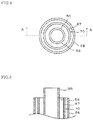
- Fig. 4 is a plan view of a periphery of jet nozzle 66
- Fig. 5 is a sectional view taken along a line A-A in Fig. 4
- Fig. 6 is a block diagram showing electrical connections of control device 82.
- FIG. 1 shows component mounter 10.
- Component mounter 10 performs mounting work of mounting an electronic component on circuit board 12 and soldering work of soldering the electronic component mounted on circuit board 12.
- Component mounter 10 includes mounting machine main body 20, board conveyance and holding device 26, component mounting device 32, mark camera 52, parts camera 54, component supply device 56, bulk component supply device 59, soldering device 60 (refer to Fig. 3 ), and control device 82 (refer to Fig. 6 ).
- the left-right direction (X axis), the front-rear direction (Y axis), and the up-down direction (Z axis) are as shown in Figs. 1 and 3 .
- Mounting machine main body 20 is made up of frame section 22, and beam section 24 provided to extend over frame section 22.
- Board conveyance and holding device 26 is provided at a center of frame section 22 in the front-rear direction and has conveyance device 28 and clamping device 30.
- Conveyance device 28 conveys circuit board 12 in the left-right direction using a conveyor belt and a shuttle arm, which are not shown.
- Conveyance device 28 conveys circuit board 12 in the left-right direction using a conveyor belt and a shuttle arm, which are not shown.
- flux is already applied to locations to be soldered, and the flux is already preheated.
- Clamping device 30 lifts up circuit board 12 from the conveyor belt and holds circuit board 12 while pressing it against a guide, not shown, or lowers circuit board 12 back onto the conveyor belt and releases circuit board 12 from being held. That is, in addition to conveying circuit board 12 in the left-right direction, board conveyance and holding device 26 also fixes and holds circuit board 12 in a predetermined position.
- Component mounting device 32 is disposed in beam section 24 and includes two work heads 34, 36 and work head moving device 40.
- suction nozzle 38 is provided on the lower end face of work heads 34, 36.
- Suction nozzle 38 picks up and holds an electronic component by negative pressure supplied from a vacuum pump, not shown, and releases the electronic component that it holds when atmospheric pressure or positive pressure is supplied thereto.
- Work head moving device 40 includes X-axis moving device 42, Y-axis moving device 44, and Z-axis moving device 46. Two work heads 34, 36 are moved together to an arbitrary position on the XY plane of frame section 22 by X-axis moving device 42 and Y-axis moving device 44. As shown in Fig.
- work heads 34, 36 are detachably mounted on sliders 48, 50, respectively, and Z-axis moving device 46 moves sliders 48, 50 in an up-down direction along slider rails 48a, 50a, respectively. This enables work heads 34, 36 to be moved individually in the up-down direction by Z-axis moving device 46.
- Mark camera 52 is mounted on slider 48 while being directed to face downwards as shown in Fig. 2 and is moved together with work head 34 in the front-rear direction, laterally, and vertically. Mark camera 52 is used to capture an image of a board mark (not shown) provided on circuit board 12 for use in positioning circuit board 12.
- parts camera 54 is installed above frame section 22 between board conveyance and holding device 26 and component supply device 56 while being directed to face upwards.
- Parts camera 54 captures images of electronic components picked up and held by suction by suction nozzles 38 of work heads 34, 36 from below when the electronic component passes over parts camera 54.
- Component supply device 56 is disposed at both ends of frame section 22 in the front-rear direction.
- tray-type component supply device 58 is disposed at a first end side and bulk component supply device 59 is disposed at a second end side of frame portion 22.
- Tray-type component supply device 58 supplies electronic components that are placed on a tray.
- Bulk component supply device 59 aligns multiple electronic components scattered in a bulky fashion and supplies electronic components that are aligned.
- a feeder-type component supply device may be provided. In the feeder-type component supply device, electronic components are supplied by a tape feeder or a stick feeder.
- Soldering device 60 is provided below conveyance device 28 and includes jet device 62 and jet device moving device 72, as shown in Fig. 3 .
- Jet device 62 includes solder bath 64, jet nozzle 66, nozzle cover 68, and gas injection section 70.
- Solder bath 64 has a substantially rectangular parallelepiped shape and reserves molten solder in the interior thereof. Jet nozzle 66 is provided on the upper surface of solder bath 64. Molten solder is pumped up from solder bath 64 by a pump (not shown) and is jetted upwards from an upper end opening of jet nozzle 66.
- cylindrical nozzle cover 68 is lower in height than jet nozzle 66 and is provided on the upper surface of solder bath 64 so as to surround jet nozzle cover 66.
- Partition pipe 67 is disposed concentrically with jet nozzle 66 between jet nozzle 66 and nozzle cover 68.
- Gas injection section 70 constitutes a section defined by an outer peripheral surface of partition pipe 67, which is lower in height than jet nozzle 66, and an inner peripheral surface of nozzle cover 68 and has an annular upper end opening.
- Gas injection section 70 is connected to a nitrogen gas cylinder, not shown. Nitrogen gas from the nitrogen gas cylinder is heated by molten solder and is then injected upwards from the annular upper end opening of gas injection section 70. Molten solder jetted from jet nozzle 66 passes through return passage 69 defined between the outer peripheral surface of jet nozzle 66 and the inner peripheral surface of partition pipe 67 to return to the interior of solder bath 64.
- jet device moving device 72 includes slider 74, X-axis moving device 76, Y-axis moving device 78, and Z-axis moving device 80.
- Slider 74 has a generally horizontal plate shape, and jet device 62 is disposed on the upper surface of slider 74.
- X-axis moving device 76 moves slider 74 in a conveyance direction of circuit board 12 by conveyance device 28, that is, in the left-right direction.
- Y-axis moving device 78 moves slider 74 in the front-rear direction.
- Z-axis moving device 80 moves slider 74 in the up-down direction.
- control device 82 is configured as a microprocessor mainly made up of CPU 82a and includes ROM 82b configured to store a process program, HDD 82c configured to store various types of data, RAM 82d configured to be used as a working region, and the like.
- Control device 82 is connected to input device 82e such as a mouse and a keyboard and display device 82f such as a liquid crystal display.
- Control device 82 is connected to board conveyance and holding device 26, component mounting device 32, mark camera 52, parts camera 54, component supply device 56, bulk component supply device 59, and soldering device 60 so that signals can be transmitted and received therebetween.
- Component mounter 10 mounts an electronic component on circuit board 12 and solders the electronic component to circuit board 12 based on a production job received from a management device, not shown, and these operations of component mounter 10 will be described below with reference to Fig. 7.
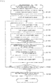
- Fig. 7 is a flow chart of a component mounting and soldering process.
- component mounter 10 can mount various types of electronic components on circuit board 12, here, a case will be described in which component mounter 10 mounts a lead component on circuit board 12 as an electronic component.
- the production job defines types of electronic components that are mounted on circuit board 12, as well as the order in which such electronic components are mounted on circuit board 12 in component mounter 10.
- CPU 82a of control device 82 reads out a program of a component mounting and soldering process routine from ROM 82b when a command to start the production job is inputted. Firstly, CPU 82a controls board conveyance and holding device 26 so that circuit board 12 is conveyed to a working position in component mounter 10 and is fixedly held by clamping device 30 in the working position (Step S100). Next, CPU 82a controls component mounting device 32 and mark camera 52 so that mark camera 52 is moved to a location above circuit board 12 to capture an image of a board mark, not shown, of circuit board 12 (Step S110). As a result, CPU 82a obtains positional information on circuit board 12 from a captured image of the board mark on circuit board 12.
- CPU 82a obtains information on a processing target lead component (Step S120).
- the information on the processing target lead component includes the type of the processing target lead component. Such information can be obtained from the production job.
- four types of lead components are to be mounted, and the four types of lead components are first to fourth lead components P1 to P4, as a matter of convenience.
- Figs. 8 to 11 show front views of lead components P1 to P4.
- First lead component P1 is such that two rectilinear leads P1b are attached to the lower surface of a rectangular parallelepiped component main body P1a, as shown in Fig. 8 .
- Second lead component P2 is a component larger in size than first lead component P1 and has two rectilinear leads P2b attached to the lower surface of component main body P2a, as shown in Fig. 9 .
- Third lead component P3 is such that two (only one is shown in Fig. 10 ) L-shaped leads P3b are attached to a lateral surface of rectangular parallelepiped component main body P3a, as shown in Fig. 10 .
- Fourth lead component P4 is such that a number of (here, six) rectilinear leads P4b are aligned in a row on the lower surface of horizontally elongated rectangular parallelepiped component main body P4a, as shown in Fig. 11 .
- CPU 82a controls component supply device 56 and bulk component supply device 59 so that a lead component is supplied to a predetermined supply position and then controls component mounting device 32 so that either of work heads 34, 36 is moved to a location above the predetermined supply position so as to pick up the lead component using suction nozzle 38 (Step S130).
- CPU 82a controls component mounting device 32 and parts camera 54 so that work heads 34, 36 holding the lead component are moved to a location above component camera 54 so that parts camera 54 captures an image of the lead component held by suction nozzle 38 (Step S140).
- CPU 82a obtains information on the orientation of the lead component or the like.
- CPU 82a controls component mounting device 32 so that work heads 34, 36 holding the lead component are moved to a location above the predetermined position on circuit board 12 (Step S150). As this occurs, CPU 82a corrects the position of work heads 34, 36 based on the information on the orientation of the lead component or the like. Following this, CPU 82a controls component mounting device 32 so that leads of the lead component picked up and held by suction nozzle 38 are inserted into through holes formed in a predetermined mounting position on circuit board 12 (Step S160). As a result, the lead component is mounted on circuit board 12.
- CPU 82a obtains a soldering parameter for the lead component mounted on circuit board 12 this time based on the information (including the type of the lead component) obtained in Step S120 (Step S170).
- the soldering parameter includes (1) a flux heating time, (2) a solder application time, (3) a solder withdrawal speed, (4) a solder curing waiting time, (5) a tracing soldering speed, (6) a height of the soldering device, and (7) a jetting height of molten solder.
- the set values for each parameter are set in accordance with the lead component type. Correspondences between the lead component types and set values for the parameters are stored in HDD 82c in the form of a table. An example of this table is shown in Fig. 12 . Each parameter will be described below.
- Flux heating time constitutes a time during which flux on circuit board 12 is heated before soldering leads of a lead component.
- Fig. 13 shows an example of heating flux F on first lead component P1.
- Lead component P1 is held by suction nozzle 38 with leads P1b inserted into through holes 14. Molten solder jetted from jet nozzle 66 does not reach the rear surface of circuit board 12.
- Through holes 14 into which leads P1b of first lead component P1 are inserted are provided in circuit board 12, and flux F is applied to peripheries of through holes 14.
- This flux F is preferably heated to an activation temperature immediately before soldering is performed.
- nitrogen gas is injected at all times from ringshaped gas injection section 70 to prevent oxidation of jetted solder.
- Control device 82 heats and activates flux F by making use of the nitrogen gas. Specifically, control device 82 controls the position of gas injection section 70 (for example, the position in the Z-axis direction) so that nitrogen gas injected from gas injection section 70 is injected against flux F applied to peripheries of through holes 14. The position of gas injection section 70 is controlled by operating jet device moving device 72.
- flux F is preheated before circuit board 12 is conveyed into component mounter 10
- flux F is deprived of heat by first lead component P1 mounted in component mounter 10, thereby reducing the temperature of flux F and causing flux F to deactivate. Since the heat capacity of a lead component increases as the size of the lead component increases, the temperature of flux F tends to be reduced to a low temperature.
- the flux heating time is set to increase the flux heating time to handle an increase in size of a lead component. For example, since second lead component P2 is larger in size than first lead component P1, the flux heating time is set to be longer for second lead component P2 than for first lead component P1.
- Solder application time constitutes a time during which molten solder is applied to the leads of the lead component which are inserted into the through holes of circuit board 12 and the peripheries of the through holes.
- Fig. 14 shows an example of soldering the leads P1b of first lead component P1.
- Lead component P1 is held by suction nozzle 38 with leads P1b inserted into through holes 14.
- Molten solder jetted from jet nozzle 66 sufficiently reaches leads P1b and the peripheries of through holes 14.
- Nitrogen gas is injected continuously from gas injection section 70 to prevent oxidation of solder or the like. To form a good fillet, molten solder is preferably applied steadily to a lead component while being kept warm.
- solder application time is set so that the solder application time is long enough to be handle an increase in size of a lead component. For example, since second lead component P2 is larger in size than first lead component P1, the soldering time is set to be longer for second lead component P2 than for first lead component P1.
- Solder withdrawal speed constitutes a speed at which jet device 62 is moved downwards below the lead component after soldering is completed.
- the solder withdrawal speed constitutes a speed at which jet device 62 is moved from a state where molten solder is applied to leads P1b and the peripheries of through holes 14 as shown in Fig. 14 to a state where molten solder does not reach leads P1b as shown in Fig. 13 .
- jet device 62 is set to be moved away from below a lead component at low speeds, to be moved away from below a lead component at high speeds, or to be moved away from below a lead component at low speeds initially and at high speeds thereafter.
- Solder curing waiting time constitutes a waiting time for solder to cure with the lead component while being kept raised from circuit board 12 and supported after soldering is completed.
- Fig. 15 shows an example of soldering L-shaped leads P3b of third lead component P3.
- jet device 62 is withdrawn low enough so that molten solder does not reach leads P3b.
- Suction nozzle 38 supports third lead component P3 while being kept raised away from circuit board 12 so that molten solder does not reach leads P3b until molten solder hardens. Since first, second, and fourth lead components P1, P2, P4, do not have to be raised from circuit board 12, the solder curing waiting time is not set therefor.
- the tracing soldering speed constitutes a speed at which jet device 62 of soldering device 60 is moved in a direction in which leads are aligned when a lead component includes a number of leads.
- Fig. 16 shows an example of soldering a number of (here, six) leads P4b of fourth lead component P4.
- fourth lead component P4 is held by suction nozzle 38 with six leads P4b inserted in six through holes 14 in circuit board 12.
- jet device 62 moves from end to end of a row where multiple leads P4b are aligned and solders leads P4b sequentially. Since first to third lead components P1 to P3 do not have to be soldered sequentially by moving jet device 62, the tracing soldering speed do not have to be set for those lead components.
- the height of a soldering device is the height of jet device 62 of soldering device 60 relative to the leads of the lead component.
- the height of jet device 62 is set so that the leads of the lead components do not interfere with jet nozzle 66. However, when leads of a lead component are long, the height of jet device 62 is set so that the leads enter inside of jet nozzle 66.
- the jetting height of molten solder constitutes a height of molten solder that is jetted from jet device 62.
- the height of molten solder jetted is set so that molten solder reaches through holes 14 in circuit board 12 into which leads are inserted.
- the height of jetted molten solder can be controlled by the pumping amount of a pump.
- CPU 82a solders the current lead component (Step S180). That is, CPU 82a performs a series of operations heating the flux based on the soldering parameter obtained in Step S170, applying the solder to the leads of the lead component and peripheries thereof, and withdrawing the solder thereafter. As this occurs, CPU 82a waits for the solder to cure as required. While soldering, suction nozzle 38 holds the lead component so that the lead component is not raised from circuit board 12. While soldering, nitrogen gas continues to be injected from gas injection section 70 without any interruption. This is because oxidation of the solder and flux is prevented by the nitrogen gas.
- CPU 82a determines whether all the mounting target components have been mounted on and soldered to circuit board 12 (Step S190), and when determining that the mounting and soldering of all the mounting target components has not yet been completed, CPU 82a returns to Step S120, where CPU 82a mounts and solders the next lead component.
- CPU 82a releases the fixing of circuit board 12 by clamping device 30 and controls board conveyance and holding device 26 so that circuit board 12 is conveyed out from the working position in component mounter 10 to an external portion thereof (Step S200), thereby ending this process routine.
- the soldering device 60 of this embodiment corresponds to a soldering device of the invention, jet device 62 to a soldering means, HDD 82c to a memory means, and CPU 82a to a control means.
- gas injection section 70 corresponds to a gas injection section, suction nozzle 38 to a component support section, and jet device moving device 72 to a moving means.
- component mounting device 32 corresponds to a component mounting device.
- leads of a lead component are soldered with a value of a soldering parameter corresponding to the lead component type. Therefore, leads of each lead component of circuit board 12 on which a number of lead components are mounted can be soldered as required.
- soldering parameters listed in the table in Fig. 12 often have different values depending on the type of lead component, applying the invention is highly meaningful.
- flux is preheated before the flux is conveyed into component mounter 10; however, the flux is deprived of heat by the lead component that is mounted within component mounter 10, thereby reducing the temperature of the flux and causing the flux to deactivate from time to time.
- the flux is heated and activated by injecting nitrogen gas heated by the heat of molten solder toward the flux. Therefore, not only can the oxidation of the flux be prevented by the nitrogen gas, but also the heat of the molten solder can be effectively used to heat the flux.
- jet device 62 can be withdrawn away from below the lead component at low speeds or high speeds, or can be withdrawn away at low speeds initially and then withdrawn away at high speeds.
- the lead component is supported in a raised state by use of suction nozzle 38 of component mounting device 32.
- suction nozzle 38 of component mounting device 32 the lead component can be reliably supported during the solder curing waiting time.
- the cost can be reduced and the size can also be made compact.
- soldering device 60 is integrated with component mounting device 32, compared with a case where both devices are provided separately, it is possible for a component to be shared, such as when suction nozzle 38 of component mounting device 32 is used as a component support section of soldering device 60. Therefore, not only a reduction in cost but also a reduction in size can be achieved. Additionally, since circuit board 12 does not have to be conveyed in and out of soldering device 60 and component mounting device 32 separately, a reduction in working time can be achieved.
- component mounting device 32 is described as including two work heads 34, 36, only one work head may be provided, or three or more work heads may be provided.
- suction nozzle 38 is described as picking up and holding electronic component by negative pressure
- a configuration may be adopted in which an openable and closable arm is utilized in place of suction nozzle 38 so that electronic component is gripped or released by closing or opening the arm.
- soldering device 60 may be configured as a single separate body.
- nitrogen gas may be injected intermittently from gas injection section 70.
- control device 82 may control gas injection section 70 so that nitrogen gas is injected during the flux heating time to heat flux F, or control device 82 may control gas injection section 70 so that nitrogen gas is not injected outside of the flux heating time.
- nitrogen gas may be applied to the periphery of flux F of circuit board 12 as shown in Fig. 13 , nitrogen gas may be applied directly to flux F.
- the invention can be applied to the electronic component industry, and more particularly to an electronic component assembler such as a chip mounter.
Landscapes
- Engineering & Computer Science (AREA)
- Mechanical Engineering (AREA)
- Manufacturing & Machinery (AREA)
- Microelectronics & Electronic Packaging (AREA)
- Electric Connection Of Electric Components To Printed Circuits (AREA)
- Molten Solder (AREA)
Abstract
Description
- The present invention relates to a soldering device
- In a case of mounting a lead component on a circuit board, leads are inserted into through holes formed in the circuit board, and the leads are soldered.
Patent Literature 1 describes a soldering device for soldering leads that are inserted in through holes by jetting molten solder towards the leads. - Patent Literature 1:
JP-A-10-209622 - Incidentally, lead components have their own appropriate parameter values that differ from lead component to lead component, and as this point has never been taken into consideration heretofore, different types of lead components have been soldered using the same parameter value. For this reason, there has been an increase in the probability of soldering defects occurring on certain types of lead components.
- The invention has been made to solve the technical problem described above, and a main object of the invention is to appropriately solder leads of each lead component of a circuit board on which a number of lead components are mounted.
- According to the invention, there is provided a soldering device comprising: a soldering means for soldering leads of multiple lead component types mounted on a board by jetting molten solder reserved in a solder bath; a memory means for storing correspondences between the lead component types and a value of a soldering parameter; and a control means configured to identify the lead component type to be soldered when sequentially soldering the multiple types of lead components by the soldering means, read out a value of the soldering parameter corresponding to the lead component type identified from the correspondences stored in the memory means, and control the soldering means so that the lead of the lead component is soldered based on the value of the soldering parameter read out.
- In sequentially soldering the multiple types of lead components using the soldering means, this soldering device identifies the type of lead component to be soldered and reads out the value of the soldering parameter that corresponds to the lead component type from the memory means. Then, the soldering device controls the soldering means so that the lead component is soldered based on the value of the soldering parameter. As a result, the lead of the lead component is soldered with the value of the soldering parameter corresponding to the type of the lead component. Therefore, according to the soldering device of the invention, leads of each lead component of a circuit board on which a number of lead components are mounted can be soldered as required.
- In the soldering device of the invention, the soldering parameter may include at least one of : a flux heating time during which flux adhering to the board is heated before the molten solder is applied to the lead of the lead component; a solder application time during which the molten solder is applied to the lead of the lead component; a solder withdrawal speed at which the soldering means is moved downwards below the lead component after the soldering means ends its soldering operation; a solder curing waiting time during which solder is allowed to cure while the lead component is supported to be raised away from the board; a tracing soldering speed at which the soldering means is moved in the direction in which leads are aligned in a case where the lead component includes a number of leads; a height of the soldering means relative to the lead of the lead component, and a jetting height of the molten solder. Since the soldering parameters listed here often differ from one lead component type to another, applying the invention is highly meaningful.
- In the soldering device of the invention, the soldering parameter may include the flux heating time, the soldering means may have a gas injecting section configured to inject a nitrogen gas heated by making use of a heat of the molten solder, and the control means may control the gas injecting section so that the nitrogen gas injected from the gas injecting section heats the flux by the flux heating time included in the value of the soldering parameter read out. Flux is preferably heated to an activation temperature at a point in time immediately before soldering is performed. In general, flux is preheated before it is conveyed into a component mounter; however, the flux is deprived of heat due to a lead component mounted inside the component mounter, thereby reducing the temperature of the flux and causing the flux to deactivate. The larger the lead component, the more heat the flux tends to be deprived of. Therefore, it is preferable to appropriately reheat and activate the flux of the lead component by setting a flux heating time corresponding to the lead component type. Here, the nitrogen gas heated by the heat of the molten solder is applied to the flux or the periphery thereof to heat and activate the flux. Therefore, not only can the oxidation of the flux be prevented by the nitrogen gas, but also the heat of the molten solder can be effectively used to heat the flux.
- The soldering device of the invention may include a moving means for moving the soldering means, wherein the soldering parameter includes the solder withdrawal speed, and the control means controls the moving means so that the soldering means is moved downwards below the lead component at the solder withdrawal speed included in the value of the soldering parameter read out. By adopting this configuration, since the solder withdrawal speed is set according to the type of the lead component, for example, the soldering means is allowed to move away from below the lead component at low speeds, move away at high speeds, or move away at low speeds initially and then to move away at high speeds.
- In the soldering device of the invention, the soldering parameter may include the solder curing waiting time, the soldering means may include a component support section configured to support the lead component to be raised away from the board, and the control means may control the component support section so that the component support section supports the lead component with being raised away from the board for the duration of the solder curing waiting time included in the value of the soldering parameter read out. By adopting this configuration, the lead component can be reliably kept raised away from the board and supported by making use of the component support section for the duration of the solder curing waiting time. In relation to a lead component that does not have to be raised away from the board, the component mounting process preferably proceeds to the next step without setting the solder curing waiting time, thereby improving the productivity.
- The soldering device of the present invention may be integrated with a component mounting device configured to hold the lead component supplied from a component supply device and move the lead component to a predetermined position on the board so that the lead of the lead component is inserted into a through hole provided in the predetermined position. By adopting this configuration, compared with a case where the component mounting device and the soldering device are provided separately, components can be processed in the common area shared between the component mounting device and the soldering device, thereby making it possible to reduce cost but also to reduce size. Further, since circuit boards do not have to be conveyed in and out of the component mounting device and the soldering device separately, working time can be reduced.
-
-
Fig. 1 is a perspective view showing a schematic configuration ofcomponent mounter 10. - [
Fig. 2] Fig. 2 is a perspective view ofcomponent mounting device 32. -
Fig. 3 is a perspective view ofsoldering device 60. -
Fig. 4 is a plan view of a periphery ofjet nozzle 66. -
Fig. 5 is a sectional view taken along line A-A inFig. 4 . -
Fig. 6 is a block diagram showing electrical connections ofcontrol device 82. -
Fig. 7 is a flow chart of a component mounting and soldering process routine. -
Fig. 8 is a front view of first lead component P1. -
Fig. 9 is a front view of second lead component P2. -
Fig. 10 is a front view of third lead component P3. -
Fig. 11 is a front view of fourth lead component P4. -
Fig. 12 is a table showing the correspondences between lead component types and soldering parameters. -
Fig. 13 is a diagram of an example of heating flux F for first lead component P1. -
Fig. 14 is a diagram of an example of soldering leads P1b of first lead component P1. -
Fig. 15 is a diagram of an example of soldering leads P3b of third lead component P3. -
Fig. 16 is a diagram of an example of soldering leads P4 of fourth lead component P4. - Referring to drawings, a preferred embodiment of the invention will be described below.
Fig. 1 is a perspective view showing a schematic configuration ofcomponent mounter 10,Fig. 2 is a perspective view (a view shown from a direction indicated by an arrow A inFig. 1 ) ofcomponent mounting device 32,Fig. 3 is a perspective view ofsoldering device 60,Fig. 4 is a plan view of a periphery ofjet nozzle 66,Fig. 5 is a sectional view taken along a line A-A inFig. 4 , andFig. 6 is a block diagram showing electrical connections ofcontrol device 82. -
FIG. 1 showscomponent mounter 10.Component mounter 10 performs mounting work of mounting an electronic component oncircuit board 12 and soldering work of soldering the electronic component mounted oncircuit board 12.Component mounter 10 includes mounting machinemain body 20, board conveyance andholding device 26,component mounting device 32,mark camera 52,parts camera 54,component supply device 56, bulkcomponent supply device 59, soldering device 60 (refer toFig. 3 ), and control device 82 (refer toFig. 6 ). In this embodiment, the left-right direction (X axis), the front-rear direction (Y axis), and the up-down direction (Z axis) are as shown inFigs. 1 and3 . - Mounting machine
main body 20 is made up of frame section 22, and beam section 24 provided to extend over frame section 22. - Board conveyance and
holding device 26 is provided at a center of frame section 22 in the front-rear direction and hasconveyance device 28 andclamping device 30.Conveyance device 28 conveyscircuit board 12 in the left-right direction using a conveyor belt and a shuttle arm, which are not shown. Oncircuit board 12 that is conveyed intocomponent mounter 10, flux is already applied to locations to be soldered, and the flux is already preheated. Clampingdevice 30 lifts upcircuit board 12 from the conveyor belt and holdscircuit board 12 while pressing it against a guide, not shown, or lowerscircuit board 12 back onto the conveyor belt and releasescircuit board 12 from being held. That is, in addition to conveyingcircuit board 12 in the left-right direction, board conveyance andholding device 26 also fixes and holdscircuit board 12 in a predetermined position. -
Component mounting device 32 is disposed in beam section 24 and includes twowork heads head moving device 40. As shown inFig. 2 ,suction nozzle 38 is provided on the lower end face of work heads 34, 36.Suction nozzle 38 picks up and holds an electronic component by negative pressure supplied from a vacuum pump, not shown, and releases the electronic component that it holds when atmospheric pressure or positive pressure is supplied thereto. Workhead moving device 40 includesX-axis moving device 42, Y-axis moving device 44, and Z-axis moving device 46. Two work heads 34, 36 are moved together to an arbitrary position on the XY plane of frame section 22 byX-axis moving device 42 and Y-axis moving device 44. As shown inFig. 2 , work heads 34, 36 are detachably mounted onsliders axis moving device 46 movessliders slider rails axis moving device 46. -
Mark camera 52 is mounted onslider 48 while being directed to face downwards as shown inFig. 2 and is moved together withwork head 34 in the front-rear direction, laterally, and vertically.Mark camera 52 is used to capture an image of a board mark (not shown) provided oncircuit board 12 for use inpositioning circuit board 12. - As shown in
Fig. 1 ,parts camera 54 is installed above frame section 22 between board conveyance and holdingdevice 26 andcomponent supply device 56 while being directed to face upwards.Parts camera 54 captures images of electronic components picked up and held by suction bysuction nozzles 38 of work heads 34, 36 from below when the electronic component passes overparts camera 54. -
Component supply device 56 is disposed at both ends of frame section 22 in the front-rear direction. InFig. 1 , tray-typecomponent supply device 58 is disposed at a first end side and bulkcomponent supply device 59 is disposed at a second end side of frame portion 22. Tray-typecomponent supply device 58 supplies electronic components that are placed on a tray. Bulkcomponent supply device 59 aligns multiple electronic components scattered in a bulky fashion and supplies electronic components that are aligned. In place of or in addition to tray-typecomponent supply device 58 and bulkcomponent supply device 59, a feeder-type component supply device may be provided. In the feeder-type component supply device, electronic components are supplied by a tape feeder or a stick feeder. -
Soldering device 60 is provided belowconveyance device 28 and includesjet device 62 and jetdevice moving device 72, as shown inFig. 3 . -
Jet device 62 includessolder bath 64,jet nozzle 66,nozzle cover 68, andgas injection section 70.Solder bath 64 has a substantially rectangular parallelepiped shape and reserves molten solder in the interior thereof.Jet nozzle 66 is provided on the upper surface ofsolder bath 64. Molten solder is pumped up fromsolder bath 64 by a pump (not shown) and is jetted upwards from an upper end opening ofjet nozzle 66. As shown inFigs. 4 and 5 ,cylindrical nozzle cover 68 is lower in height thanjet nozzle 66 and is provided on the upper surface ofsolder bath 64 so as to surroundjet nozzle cover 66.Partition pipe 67 is disposed concentrically withjet nozzle 66 betweenjet nozzle 66 andnozzle cover 68.Gas injection section 70 constitutes a section defined by an outer peripheral surface ofpartition pipe 67, which is lower in height thanjet nozzle 66, and an inner peripheral surface ofnozzle cover 68 and has an annular upper end opening.Gas injection section 70 is connected to a nitrogen gas cylinder, not shown. Nitrogen gas from the nitrogen gas cylinder is heated by molten solder and is then injected upwards from the annular upper end opening ofgas injection section 70. Molten solder jetted fromjet nozzle 66 passes throughreturn passage 69 defined between the outer peripheral surface ofjet nozzle 66 and the inner peripheral surface ofpartition pipe 67 to return to the interior ofsolder bath 64. - As shown in
Fig. 3 , jetdevice moving device 72 includesslider 74,X-axis moving device 76, Y-axis moving device 78, and Z-axis moving device 80.Slider 74 has a generally horizontal plate shape, andjet device 62 is disposed on the upper surface ofslider 74.X-axis moving device 76moves slider 74 in a conveyance direction ofcircuit board 12 byconveyance device 28, that is, in the left-right direction. Y-axis moving device 78moves slider 74 in the front-rear direction. Further, Z-axis moving device 80moves slider 74 in the up-down direction. By using these moving devices,jet device 62 is moved to any position below conveyance device 28 (refer toFig. 1 ) by the action of jetdevice moving device 72. - As shown in
Fig. 6 ,control device 82 is configured as a microprocessor mainly made up ofCPU 82a and includesROM 82b configured to store a process program,HDD 82c configured to store various types of data, RAM 82d configured to be used as a working region, and the like.Control device 82 is connected to input device 82e such as a mouse and a keyboard and display device 82f such as a liquid crystal display.Control device 82 is connected to board conveyance and holdingdevice 26,component mounting device 32,mark camera 52,parts camera 54,component supply device 56, bulkcomponent supply device 59, andsoldering device 60 so that signals can be transmitted and received therebetween. -
Component mounter 10 mounts an electronic component oncircuit board 12 and solders the electronic component tocircuit board 12 based on a production job received from a management device, not shown, and these operations ofcomponent mounter 10 will be described below with reference toFig. 7. Fig. 7 is a flow chart of a component mounting and soldering process. Althoughcomponent mounter 10 can mount various types of electronic components oncircuit board 12, here, a case will be described in whichcomponent mounter 10 mounts a lead component oncircuit board 12 as an electronic component. The production job defines types of electronic components that are mounted oncircuit board 12, as well as the order in which such electronic components are mounted oncircuit board 12 incomponent mounter 10. -
CPU 82a ofcontrol device 82 reads out a program of a component mounting and soldering process routine fromROM 82b when a command to start the production job is inputted. Firstly,CPU 82a controls board conveyance and holdingdevice 26 so thatcircuit board 12 is conveyed to a working position incomponent mounter 10 and is fixedly held by clampingdevice 30 in the working position (Step S100). Next,CPU 82a controlscomponent mounting device 32 andmark camera 52 so thatmark camera 52 is moved to a location abovecircuit board 12 to capture an image of a board mark, not shown, of circuit board 12 (Step S110). As a result,CPU 82a obtains positional information oncircuit board 12 from a captured image of the board mark oncircuit board 12. - Next,
CPU 82a obtains information on a processing target lead component (Step S120). The information on the processing target lead component includes the type of the processing target lead component. Such information can be obtained from the production job. In this embodiment, four types of lead components are to be mounted, and the four types of lead components are first to fourth lead components P1 to P4, as a matter of convenience.Figs. 8 to 11 show front views of lead components P1 to P4. First lead component P1 is such that two rectilinear leads P1b are attached to the lower surface of a rectangular parallelepiped component main body P1a, as shown inFig. 8 . Second lead component P2 is a component larger in size than first lead component P1 and has two rectilinear leads P2b attached to the lower surface of component main body P2a, as shown inFig. 9 . Third lead component P3 is such that two (only one is shown inFig. 10 ) L-shaped leads P3b are attached to a lateral surface of rectangular parallelepiped component main body P3a, as shown inFig. 10 . Fourth lead component P4 is such that a number of (here, six) rectilinear leads P4b are aligned in a row on the lower surface of horizontally elongated rectangular parallelepiped component main body P4a, as shown inFig. 11 . - Next,
CPU 82a controlscomponent supply device 56 and bulkcomponent supply device 59 so that a lead component is supplied to a predetermined supply position and then controlscomponent mounting device 32 so that either of work heads 34, 36 is moved to a location above the predetermined supply position so as to pick up the lead component using suction nozzle 38 (Step S130). Following this,CPU 82a controlscomponent mounting device 32 andparts camera 54 so that work heads 34, 36 holding the lead component are moved to a location abovecomponent camera 54 so thatparts camera 54 captures an image of the lead component held by suction nozzle 38 (Step S140). As a result,CPU 82a obtains information on the orientation of the lead component or the like. Following this,CPU 82a controlscomponent mounting device 32 so that work heads 34, 36 holding the lead component are moved to a location above the predetermined position on circuit board 12 (Step S150). As this occurs,CPU 82a corrects the position of work heads 34, 36 based on the information on the orientation of the lead component or the like. Following this,CPU 82a controlscomponent mounting device 32 so that leads of the lead component picked up and held bysuction nozzle 38 are inserted into through holes formed in a predetermined mounting position on circuit board 12 (Step S160). As a result, the lead component is mounted oncircuit board 12. - Next,
CPU 82a obtains a soldering parameter for the lead component mounted oncircuit board 12 this time based on the information (including the type of the lead component) obtained in Step S120 (Step S170). The soldering parameter includes (1) a flux heating time, (2) a solder application time, (3) a solder withdrawal speed, (4) a solder curing waiting time, (5) a tracing soldering speed, (6) a height of the soldering device, and (7) a jetting height of molten solder. The set values for each parameter are set in accordance with the lead component type. Correspondences between the lead component types and set values for the parameters are stored inHDD 82c in the form of a table. An example of this table is shown inFig. 12 . Each parameter will be described below. - Flux heating time constitutes a time during which flux on
circuit board 12 is heated before soldering leads of a lead component.Fig. 13 shows an example of heating flux F on first lead component P1. Lead component P1 is held bysuction nozzle 38 with leads P1b inserted into throughholes 14. Molten solder jetted fromjet nozzle 66 does not reach the rear surface ofcircuit board 12. Throughholes 14 into which leads P1b of first lead component P1 are inserted are provided incircuit board 12, and flux F is applied to peripheries of throughholes 14. This flux F is preferably heated to an activation temperature immediately before soldering is performed. In this embodiment, nitrogen gas is injected at all times from ringshapedgas injection section 70 to prevent oxidation of jetted solder.Control device 82 heats and activates flux F by making use of the nitrogen gas. Specifically,control device 82 controls the position of gas injection section 70 (for example, the position in the Z-axis direction) so that nitrogen gas injected fromgas injection section 70 is injected against flux F applied to peripheries of throughholes 14. The position ofgas injection section 70 is controlled by operating jetdevice moving device 72. Although flux F is preheated beforecircuit board 12 is conveyed intocomponent mounter 10, flux F is deprived of heat by first lead component P1 mounted incomponent mounter 10, thereby reducing the temperature of flux F and causing flux F to deactivate. Since the heat capacity of a lead component increases as the size of the lead component increases, the temperature of flux F tends to be reduced to a low temperature. For this reason, the flux heating time is set to increase the flux heating time to handle an increase in size of a lead component. For example, since second lead component P2 is larger in size than first lead component P1, the flux heating time is set to be longer for second lead component P2 than for first lead component P1. - Solder application time constitutes a time during which molten solder is applied to the leads of the lead component which are inserted into the through holes of
circuit board 12 and the peripheries of the through holes.Fig. 14 shows an example of soldering the leads P1b of first lead component P1. Lead component P1 is held bysuction nozzle 38 with leads P1b inserted into throughholes 14. Molten solder jetted fromjet nozzle 66 sufficiently reaches leads P1b and the peripheries of throughholes 14. Nitrogen gas is injected continuously fromgas injection section 70 to prevent oxidation of solder or the like. To form a good fillet, molten solder is preferably applied steadily to a lead component while being kept warm. The thermal capacity of a lead component increases as the size thereof increases,and hence, a large lead component tends to be difficult to warm. Therefore, a solder application time is set so that the solder application time is long enough to be handle an increase in size of a lead component. For example, since second lead component P2 is larger in size than first lead component P1, the soldering time is set to be longer for second lead component P2 than for first lead component P1. - Solder withdrawal speed constitutes a speed at which
jet device 62 is moved downwards below the lead component after soldering is completed. For example, the solder withdrawal speed constitutes a speed at whichjet device 62 is moved from a state where molten solder is applied to leads P1b and the peripheries of throughholes 14 as shown inFig. 14 to a state where molten solder does not reach leads P1b as shown inFig. 13 . Depending on types of lead components,jet device 62 is set to be moved away from below a lead component at low speeds, to be moved away from below a lead component at high speeds, or to be moved away from below a lead component at low speeds initially and at high speeds thereafter. - Solder curing waiting time constitutes a waiting time for solder to cure with the lead component while being kept raised from
circuit board 12 and supported after soldering is completed.Fig. 15 shows an example of soldering L-shaped leads P3b of third lead component P3. Here,jet device 62 is withdrawn low enough so that molten solder does not reach leads P3b.Suction nozzle 38 supports third lead component P3 while being kept raised away fromcircuit board 12 so that molten solder does not reach leads P3b until molten solder hardens. Since first, second, and fourth lead components P1, P2, P4, do not have to be raised fromcircuit board 12, the solder curing waiting time is not set therefor. - The tracing soldering speed constitutes a speed at which
jet device 62 ofsoldering device 60 is moved in a direction in which leads are aligned when a lead component includes a number of leads.Fig. 16 shows an example of soldering a number of (here, six) leads P4b of fourth lead component P4. InFig. 16 , fourth lead component P4 is held bysuction nozzle 38 with six leads P4b inserted in six throughholes 14 incircuit board 12. In this state,jet device 62 moves from end to end of a row where multiple leads P4b are aligned and solders leads P4b sequentially. Since first to third lead components P1 to P3 do not have to be soldered sequentially by movingjet device 62, the tracing soldering speed do not have to be set for those lead components. - The height of a soldering device is the height of
jet device 62 ofsoldering device 60 relative to the leads of the lead component. The height ofjet device 62 is set so that the leads of the lead components do not interfere withjet nozzle 66. However, when leads of a lead component are long, the height ofjet device 62 is set so that the leads enter inside ofjet nozzle 66. - The jetting height of molten solder constitutes a height of molten solder that is jetted from
jet device 62. The height of molten solder jetted is set so that molten solder reaches throughholes 14 incircuit board 12 into which leads are inserted. The height of jetted molten solder can be controlled by the pumping amount of a pump. - Then,
CPU 82a solders the current lead component (Step S180). That is,CPU 82a performs a series of operations heating the flux based on the soldering parameter obtained in Step S170, applying the solder to the leads of the lead component and peripheries thereof, and withdrawing the solder thereafter. As this occurs,CPU 82a waits for the solder to cure as required. While soldering,suction nozzle 38 holds the lead component so that the lead component is not raised fromcircuit board 12. While soldering, nitrogen gas continues to be injected fromgas injection section 70 without any interruption. This is because oxidation of the solder and flux is prevented by the nitrogen gas. - Subsequently,
CPU 82a determines whether all the mounting target components have been mounted on and soldered to circuit board 12 (Step S190), and when determining that the mounting and soldering of all the mounting target components has not yet been completed,CPU 82a returns to Step S120, whereCPU 82a mounts and solders the next lead component. On the other hand, when it is determined that the mounting and soldering of all the mounting target components that are to be mounted oncircuit board 12 has been completed,CPU 82a releases the fixing ofcircuit board 12 by clampingdevice 30 and controls board conveyance and holdingdevice 26 so thatcircuit board 12 is conveyed out from the working position incomponent mounter 10 to an external portion thereof (Step S200), thereby ending this process routine. - Here, correspondence between the constituent elements of the embodiment and constituent elements of the invention will be described. The
soldering device 60 of this embodiment corresponds to a soldering device of the invention,jet device 62 to a soldering means,HDD 82c to a memory means, andCPU 82a to a control means. In addition,gas injection section 70 corresponds to a gas injection section,suction nozzle 38 to a component support section, and jetdevice moving device 72 to a moving means. Further,component mounting device 32 corresponds to a component mounting device. - According to
component mounter 10 of the embodiment that has been described heretofore, leads of a lead component are soldered with a value of a soldering parameter corresponding to the lead component type. Therefore, leads of each lead component ofcircuit board 12 on which a number of lead components are mounted can be soldered as required. In particular, since the soldering parameters listed in the table inFig. 12 often have different values depending on the type of lead component, applying the invention is highly meaningful. - Normally, flux is preheated before the flux is conveyed into
component mounter 10; however, the flux is deprived of heat by the lead component that is mounted withincomponent mounter 10, thereby reducing the temperature of the flux and causing the flux to deactivate from time to time. The larger the lead component, the more heat the flux tends to be deprived of. Therefore, it is preferable to appropriately reheat and activate the flux of the lead component by setting a flux heating time corresponding to the lead component type. Here, the flux is heated and activated by injecting nitrogen gas heated by the heat of molten solder toward the flux. Therefore, not only can the oxidation of the flux be prevented by the nitrogen gas, but also the heat of the molten solder can be effectively used to heat the flux. - Furthermore, since the solder withdrawal speed is set according to the type of lead component, for example,
jet device 62 can be withdrawn away from below the lead component at low speeds or high speeds, or can be withdrawn away at low speeds initially and then withdrawn away at high speeds. - Furthermore, for a lead component like third lead component P3 that needs to be cured while being supported in a raised state after solder is applied, the lead component is supported in a raised state by use of
suction nozzle 38 ofcomponent mounting device 32. As a result, the lead component can be reliably supported during the solder curing waiting time. In addition, since no other component support section thansuction nozzle 38 needs to be provided, the cost can be reduced and the size can also be made compact. - Then, since soldering
device 60 is integrated withcomponent mounting device 32, compared with a case where both devices are provided separately, it is possible for a component to be shared, such as whensuction nozzle 38 ofcomponent mounting device 32 is used as a component support section ofsoldering device 60. Therefore, not only a reduction in cost but also a reduction in size can be achieved. Additionally, sincecircuit board 12 does not have to be conveyed in and out ofsoldering device 60 andcomponent mounting device 32 separately, a reduction in working time can be achieved. - The invention is not limited to the embodiment described above, and the invention can be carried out in various forms without departing from the sprit and technical scope of the invention.
- For example, in the embodiment described above, while
component mounting device 32 is described as including two work heads 34, 36, only one work head may be provided, or three or more work heads may be provided. - In the embodiment described above, while
suction nozzle 38 is described as picking up and holding electronic component by negative pressure, a configuration may be adopted in which an openable and closable arm is utilized in place ofsuction nozzle 38 so that electronic component is gripped or released by closing or opening the arm. - In the embodiment described above, while
component mounter 10 is described as havingsoldering device 60 andcomponent mounting device 32 integrated with each other,soldering device 60 may be configured as a single separate body. - In the embodiment described above, while nitrogen gas is described as being injected from
gas injection section 70 at all times, nitrogen gas may be injected intermittently fromgas injection section 70. For example,control device 82 may controlgas injection section 70 so that nitrogen gas is injected during the flux heating time to heat flux F, orcontrol device 82 may controlgas injection section 70 so that nitrogen gas is not injected outside of the flux heating time. Although nitrogen gas may be applied to the periphery of flux F ofcircuit board 12 as shown inFig. 13 , nitrogen gas may be applied directly to flux F. - The invention can be applied to the electronic component industry, and more particularly to an electronic component assembler such as a chip mounter.
- 10 component mounter, 12 circuit board, 14 through hole, 20 mounting machine main body, 22 frame section, 24 beam section, 26 board conveyance and holding device, 28 conveyance device, 30 clamping device, 32 component mounting device, 34, 36 work head, 38 suction nozzle, 40 work head moving device, 42 X-axis moving device, 44 Y-axis moving device, 46 Z-axis moving device48, 50 slider, 48a, 50a slider rail, 52mark camera, 54 parts camera, 56 component supply device, 58 tray-type component supply device, 59 bulk component supply device, 60 soldering device, 62 jet device, 64 solder bath, 66 jet nozzle, 67 partition pipe, 68 nozzle cover, 69 return passage, 70 gas injection section, 72 jet device moving device, 74 slider, 76 X-axis moving device, 78 Y-axis moving device, 80 Z-axis moving device, 82 control device, 82a CPU, 82b ROM, 82c HDD, 82d RAM, 82e input device, 82f display device, F flux, P1 to P4 first to fourth lead components, P1a to P4a component main body, P1b to P4b lead.
Claims (6)
- A soldering device comprising:a soldering means for soldering leads of multiple lead component types mounted on a board by jetting molten solder reserved in a solder bath;a memory means for storing correspondences between the lead component types and a value of a soldering parameter; anda control means configured to identify the lead component type to be soldered when sequentially soldering the multiple types of lead components by the soldering means, read out a value of the soldering parameter corresponding to the lead component type identified from the correspondences stored in the memory means, and control the soldering means so that the lead of the lead component is soldered based on the value of the soldering parameter read out.
- The soldering device of claim 1, wherein the soldering parameter may include at least one of:a flux heating time during which flux adhering to the board is heated before the molten solder is applied to the lead of the lead component;a solder application time during which the molten solder is applied to the lead of the lead component;a solder withdrawal speed at which the soldering means is moved downwards below the lead component after the soldering means ends its soldering operation;a solder curing waiting time during which solder is allowed to cure while the lead component is supported to be raised from the board;a tracing soldering speed at which the soldering means is moved in the direction in which leads are aligned in a case where the lead component includes a number of leads;a height of the soldering means relative to the lead of the lead component, anda jetting height of the molten solder.
- The soldering device according to claim 2, wherein the soldering parameter includes the flux heating time, the soldering means has a gas injecting section configured to inject nitrogen gas heated by heat of the molten solder, and
the control means controls the gas injecting section so that the nitrogen gas injected from the gas injecting section heats the flux during the flux heating time included in the value of the soldering parameter read out. - The soldering device according to Claim 2 or 3, comprising: a moving means configured to move the soldering means, wherein the soldering parameter includes the solder withdrawal speed, and the control means controls the moving means so that the soldering means is moved downwards below the lead component at the solder withdrawal speed included in the value of the soldering parameter read out.
- The soldering device according to any one of Claims 1 to 4, wherein the soldering parameter includes the solder curing waiting time, the soldering means having a component support section configured to support the lead component to be raised away from the board, and the control means controls the component support section so that the component support section supports the lead component with being raised away from the board for the duration of the solder curing waiting time included in the value of the soldering parameter read out.
- The soldering device according to any one of claims 1 to 5, wherein
the soldering device being integrated with a component mounting device configured to hold the lead component supplied from a component supply device and move the lead component to a predetermined position on the board so that the lead of the lead component is inserted into a through hole provided in the predetermined position.
Applications Claiming Priority (1)
| Application Number | Priority Date | Filing Date | Title |
|---|---|---|---|
| PCT/JP2016/072554 WO2018025314A1 (en) | 2016-08-01 | 2016-08-01 | Soldering device |
Publications (3)
| Publication Number | Publication Date |
|---|---|
| EP3493658A1 true EP3493658A1 (en) | 2019-06-05 |
| EP3493658A4 EP3493658A4 (en) | 2019-08-14 |
| EP3493658B1 EP3493658B1 (en) | 2023-03-08 |
Family
ID=61073707
Family Applications (1)
| Application Number | Title | Priority Date | Filing Date |
|---|---|---|---|
| EP16911575.5A Active EP3493658B1 (en) | 2016-08-01 | 2016-08-01 | Soldering device |
Country Status (5)
| Country | Link |
|---|---|
| US (1) | US10569351B2 (en) |
| EP (1) | EP3493658B1 (en) |
| JP (1) | JP6788674B2 (en) |
| CN (1) | CN109565938B (en) |
| WO (1) | WO2018025314A1 (en) |
Families Citing this family (6)
| Publication number | Priority date | Publication date | Assignee | Title |
|---|---|---|---|---|
| JP6849909B2 (en) * | 2017-02-07 | 2021-03-31 | 富士通株式会社 | Soldering method, soldering equipment, and method of keeping the solder wet of the jet nozzle |
| US10780515B2 (en) | 2018-04-26 | 2020-09-22 | Raytheon Technologies Corporation | Auto-adaptive braze dispensing systems and methods |
| CN110282341A (en) * | 2019-06-25 | 2019-09-27 | 英业达科技有限公司 | Fetching device |
| JP7209094B2 (en) * | 2019-07-24 | 2023-01-19 | 株式会社Fuji | Information processing device, information processing method and program |
| GB2588599B (en) * | 2019-10-24 | 2021-11-17 | Apollo Fire Detectors Ltd | Soldering Process |
| CN118789080B (en) * | 2024-08-20 | 2025-08-01 | 山东鲁华容器有限公司 | Arc welding machine for processing liquefied gas steel cylinders and operation method thereof |
Family Cites Families (9)
| Publication number | Priority date | Publication date | Assignee | Title |
|---|---|---|---|---|
| US4890781A (en) | 1988-08-04 | 1990-01-02 | Texas Instruments Incorporated | Automated flow solder machine |
| JPH10209622A (en) | 1997-01-27 | 1998-08-07 | Denso Corp | How to mount insertable parts |
| US6367677B1 (en) | 1999-09-28 | 2002-04-09 | Hill-Rom Services, Inc. | Wave solder apparatus and method |
| JP2005167142A (en) * | 2003-12-05 | 2005-06-23 | Nec Tohoku Ltd | Soldering equipment |
| JP2006156767A (en) | 2004-11-30 | 2006-06-15 | Hitachi Ltd | Soldering equipment |
| JP2008109034A (en) * | 2006-10-27 | 2008-05-08 | Koki Tec Corp | Solder jet nozzle and soldering device |
| JP5121954B2 (en) | 2010-03-31 | 2013-01-16 | パナソニック株式会社 | Point solder NC data creation method |
| JP2011254034A (en) * | 2010-06-04 | 2011-12-15 | Fuji Electric Co Ltd | Flow soldering method |
| JP2014130948A (en) * | 2012-12-28 | 2014-07-10 | Toshiba Corp | Component mounting device, component mounting system, and component mounting method |
-
2016
- 2016-08-01 CN CN201680088148.2A patent/CN109565938B/en active Active
- 2016-08-01 US US16/321,981 patent/US10569351B2/en active Active
- 2016-08-01 EP EP16911575.5A patent/EP3493658B1/en active Active
- 2016-08-01 JP JP2018531002A patent/JP6788674B2/en active Active
- 2016-08-01 WO PCT/JP2016/072554 patent/WO2018025314A1/en not_active Ceased
Also Published As
| Publication number | Publication date |
|---|---|
| CN109565938A (en) | 2019-04-02 |
| EP3493658B1 (en) | 2023-03-08 |
| WO2018025314A1 (en) | 2018-02-08 |
| EP3493658A4 (en) | 2019-08-14 |
| US20190176256A1 (en) | 2019-06-13 |
| US10569351B2 (en) | 2020-02-25 |
| JP6788674B2 (en) | 2020-11-25 |
| JPWO2018025314A1 (en) | 2019-05-23 |
| CN109565938B (en) | 2022-06-03 |
Similar Documents
| Publication | Publication Date | Title |
|---|---|---|
| EP3493658B1 (en) | Soldering device | |
| CN108886888B (en) | Action confirmation device of electronic component mounting machine | |
| EP3522687B1 (en) | Machine for performing work on substrate, and insertion method | |
| JP4126762B2 (en) | Electronic component mounting method | |
| US10506750B2 (en) | Board work machine and recognition method | |
| JP6009695B2 (en) | Component mounting apparatus and component mounting method | |
| EP3291658B1 (en) | Working machine | |
| US20230247772A1 (en) | Coating device and component mounting machine | |
| EP3310147B1 (en) | Component mounting machine | |
| US10959361B2 (en) | Substrate working machine | |
| JP6259331B2 (en) | Component mounting equipment | |
| JP6307278B2 (en) | Surface mounter and position shift detection method | |
| JP2019057685A (en) | Component mounting apparatus and mounting board manufacturing method | |
| JP6714730B2 (en) | Working machine and soldering method | |
| EP4734691A1 (en) | Component mounter and component mounting method | |
| WO2016056045A1 (en) | Substrate working machine and mounting method | |
| CN114208406A (en) | Substrate working machine | |
| JP2004311554A (en) | Device and method for mounting electronic component | |
| JP2004111448A (en) | Component mounting device | |
| EP3826446A1 (en) | Component supply device | |
| JP2017017349A (en) | Component mounting equipment |
Legal Events
| Date | Code | Title | Description |
|---|---|---|---|
| STAA | Information on the status of an ep patent application or granted ep patent |
Free format text: STATUS: THE INTERNATIONAL PUBLICATION HAS BEEN MADE |
|
| PUAI | Public reference made under article 153(3) epc to a published international application that has entered the european phase |
Free format text: ORIGINAL CODE: 0009012 |
|
| STAA | Information on the status of an ep patent application or granted ep patent |
Free format text: STATUS: REQUEST FOR EXAMINATION WAS MADE |
|
| 17P | Request for examination filed |
Effective date: 20190130 |
|
| AK | Designated contracting states |
Kind code of ref document: A1 Designated state(s): AL AT BE BG CH CY CZ DE DK EE ES FI FR GB GR HR HU IE IS IT LI LT LU LV MC MK MT NL NO PL PT RO RS SE SI SK SM TR |
|
| AX | Request for extension of the european patent |
Extension state: BA ME |
|
| A4 | Supplementary search report drawn up and despatched |
Effective date: 20190716 |
|
| RIC1 | Information provided on ipc code assigned before grant |
Ipc: B23K 3/06 20060101ALI20190710BHEP Ipc: B23K 101/42 20060101ALN20190710BHEP Ipc: B23K 1/08 20060101ALI20190710BHEP Ipc: B23K 1/00 20060101ALI20190710BHEP Ipc: H05K 3/34 20060101AFI20190710BHEP Ipc: B23K 101/40 20060101ALN20190710BHEP |
|
| DAV | Request for validation of the european patent (deleted) | ||
| DAX | Request for extension of the european patent (deleted) | ||
| GRAP | Despatch of communication of intention to grant a patent |
Free format text: ORIGINAL CODE: EPIDOSNIGR1 |
|
| STAA | Information on the status of an ep patent application or granted ep patent |
Free format text: STATUS: GRANT OF PATENT IS INTENDED |
|
| RIC1 | Information provided on ipc code assigned before grant |
Ipc: B23K 101/40 20060101ALN20220906BHEP Ipc: B23K 101/42 20060101ALN20220906BHEP Ipc: B23K 3/06 20060101ALI20220906BHEP Ipc: B23K 1/08 20060101ALI20220906BHEP Ipc: B23K 1/00 20060101ALI20220906BHEP Ipc: H05K 3/34 20060101AFI20220906BHEP |
|
| INTG | Intention to grant announced |
Effective date: 20220922 |
|
| GRAS | Grant fee paid |
Free format text: ORIGINAL CODE: EPIDOSNIGR3 |
|
| GRAA | (expected) grant |
Free format text: ORIGINAL CODE: 0009210 |
|
| STAA | Information on the status of an ep patent application or granted ep patent |
Free format text: STATUS: THE PATENT HAS BEEN GRANTED |
|
| AK | Designated contracting states |
Kind code of ref document: B1 Designated state(s): AL AT BE BG CH CY CZ DE DK EE ES FI FR GB GR HR HU IE IS IT LI LT LU LV MC MK MT NL NO PL PT RO RS SE SI SK SM TR |
|
| REG | Reference to a national code |
Ref country code: GB Ref legal event code: FG4D |
|
| REG | Reference to a national code |
Ref country code: CH Ref legal event code: EP Ref country code: AT Ref legal event code: REF Ref document number: 1553447 Country of ref document: AT Kind code of ref document: T Effective date: 20230315 |
|
| REG | Reference to a national code |
Ref country code: DE Ref legal event code: R096 Ref document number: 602016078252 Country of ref document: DE |
|
| REG | Reference to a national code |
Ref country code: IE Ref legal event code: FG4D |
|
| P01 | Opt-out of the competence of the unified patent court (upc) registered |
Effective date: 20230328 |
|
| REG | Reference to a national code |
Ref country code: LT Ref legal event code: MG9D |
|
| REG | Reference to a national code |
Ref country code: NL Ref legal event code: MP Effective date: 20230308 |
|
| PG25 | Lapsed in a contracting state [announced via postgrant information from national office to epo] |
Ref country code: RS Free format text: LAPSE BECAUSE OF FAILURE TO SUBMIT A TRANSLATION OF THE DESCRIPTION OR TO PAY THE FEE WITHIN THE PRESCRIBED TIME-LIMIT Effective date: 20230308 Ref country code: NO Free format text: LAPSE BECAUSE OF FAILURE TO SUBMIT A TRANSLATION OF THE DESCRIPTION OR TO PAY THE FEE WITHIN THE PRESCRIBED TIME-LIMIT Effective date: 20230608 Ref country code: LV Free format text: LAPSE BECAUSE OF FAILURE TO SUBMIT A TRANSLATION OF THE DESCRIPTION OR TO PAY THE FEE WITHIN THE PRESCRIBED TIME-LIMIT Effective date: 20230308 Ref country code: LT Free format text: LAPSE BECAUSE OF FAILURE TO SUBMIT A TRANSLATION OF THE DESCRIPTION OR TO PAY THE FEE WITHIN THE PRESCRIBED TIME-LIMIT Effective date: 20230308 Ref country code: HR Free format text: LAPSE BECAUSE OF FAILURE TO SUBMIT A TRANSLATION OF THE DESCRIPTION OR TO PAY THE FEE WITHIN THE PRESCRIBED TIME-LIMIT Effective date: 20230308 Ref country code: ES Free format text: LAPSE BECAUSE OF FAILURE TO SUBMIT A TRANSLATION OF THE DESCRIPTION OR TO PAY THE FEE WITHIN THE PRESCRIBED TIME-LIMIT Effective date: 20230308 |
|
| REG | Reference to a national code |
Ref country code: AT Ref legal event code: MK05 Ref document number: 1553447 Country of ref document: AT Kind code of ref document: T Effective date: 20230308 |
|
| PG25 | Lapsed in a contracting state [announced via postgrant information from national office to epo] |
Ref country code: SE Free format text: LAPSE BECAUSE OF FAILURE TO SUBMIT A TRANSLATION OF THE DESCRIPTION OR TO PAY THE FEE WITHIN THE PRESCRIBED TIME-LIMIT Effective date: 20230308 Ref country code: NL Free format text: LAPSE BECAUSE OF FAILURE TO SUBMIT A TRANSLATION OF THE DESCRIPTION OR TO PAY THE FEE WITHIN THE PRESCRIBED TIME-LIMIT Effective date: 20230308 Ref country code: GR Free format text: LAPSE BECAUSE OF FAILURE TO SUBMIT A TRANSLATION OF THE DESCRIPTION OR TO PAY THE FEE WITHIN THE PRESCRIBED TIME-LIMIT Effective date: 20230609 Ref country code: FI Free format text: LAPSE BECAUSE OF FAILURE TO SUBMIT A TRANSLATION OF THE DESCRIPTION OR TO PAY THE FEE WITHIN THE PRESCRIBED TIME-LIMIT Effective date: 20230308 |
|
| PG25 | Lapsed in a contracting state [announced via postgrant information from national office to epo] |
Ref country code: SM Free format text: LAPSE BECAUSE OF FAILURE TO SUBMIT A TRANSLATION OF THE DESCRIPTION OR TO PAY THE FEE WITHIN THE PRESCRIBED TIME-LIMIT Effective date: 20230308 Ref country code: RO Free format text: LAPSE BECAUSE OF FAILURE TO SUBMIT A TRANSLATION OF THE DESCRIPTION OR TO PAY THE FEE WITHIN THE PRESCRIBED TIME-LIMIT Effective date: 20230308 Ref country code: PT Free format text: LAPSE BECAUSE OF FAILURE TO SUBMIT A TRANSLATION OF THE DESCRIPTION OR TO PAY THE FEE WITHIN THE PRESCRIBED TIME-LIMIT Effective date: 20230710 Ref country code: EE Free format text: LAPSE BECAUSE OF FAILURE TO SUBMIT A TRANSLATION OF THE DESCRIPTION OR TO PAY THE FEE WITHIN THE PRESCRIBED TIME-LIMIT Effective date: 20230308 Ref country code: CZ Free format text: LAPSE BECAUSE OF FAILURE TO SUBMIT A TRANSLATION OF THE DESCRIPTION OR TO PAY THE FEE WITHIN THE PRESCRIBED TIME-LIMIT Effective date: 20230308 Ref country code: AT Free format text: LAPSE BECAUSE OF FAILURE TO SUBMIT A TRANSLATION OF THE DESCRIPTION OR TO PAY THE FEE WITHIN THE PRESCRIBED TIME-LIMIT Effective date: 20230308 |
|
| PG25 | Lapsed in a contracting state [announced via postgrant information from national office to epo] |
Ref country code: SK Free format text: LAPSE BECAUSE OF FAILURE TO SUBMIT A TRANSLATION OF THE DESCRIPTION OR TO PAY THE FEE WITHIN THE PRESCRIBED TIME-LIMIT Effective date: 20230308 Ref country code: PL Free format text: LAPSE BECAUSE OF FAILURE TO SUBMIT A TRANSLATION OF THE DESCRIPTION OR TO PAY THE FEE WITHIN THE PRESCRIBED TIME-LIMIT Effective date: 20230308 Ref country code: IS Free format text: LAPSE BECAUSE OF FAILURE TO SUBMIT A TRANSLATION OF THE DESCRIPTION OR TO PAY THE FEE WITHIN THE PRESCRIBED TIME-LIMIT Effective date: 20230708 |
|
| REG | Reference to a national code |
Ref country code: DE Ref legal event code: R097 Ref document number: 602016078252 Country of ref document: DE |
|
| PLBE | No opposition filed within time limit |
Free format text: ORIGINAL CODE: 0009261 |
|
| STAA | Information on the status of an ep patent application or granted ep patent |
Free format text: STATUS: NO OPPOSITION FILED WITHIN TIME LIMIT |
|
| PG25 | Lapsed in a contracting state [announced via postgrant information from national office to epo] |
Ref country code: SI Free format text: LAPSE BECAUSE OF FAILURE TO SUBMIT A TRANSLATION OF THE DESCRIPTION OR TO PAY THE FEE WITHIN THE PRESCRIBED TIME-LIMIT Effective date: 20230308 Ref country code: DK Free format text: LAPSE BECAUSE OF FAILURE TO SUBMIT A TRANSLATION OF THE DESCRIPTION OR TO PAY THE FEE WITHIN THE PRESCRIBED TIME-LIMIT Effective date: 20230308 |
|
| 26N | No opposition filed |
Effective date: 20231211 |
|
| PG25 | Lapsed in a contracting state [announced via postgrant information from national office to epo] |
Ref country code: MC Free format text: LAPSE BECAUSE OF FAILURE TO SUBMIT A TRANSLATION OF THE DESCRIPTION OR TO PAY THE FEE WITHIN THE PRESCRIBED TIME-LIMIT Effective date: 20230308 |
|
| REG | Reference to a national code |
Ref country code: CH Ref legal event code: PL |
|
| PG25 | Lapsed in a contracting state [announced via postgrant information from national office to epo] |
Ref country code: MC Free format text: LAPSE BECAUSE OF FAILURE TO SUBMIT A TRANSLATION OF THE DESCRIPTION OR TO PAY THE FEE WITHIN THE PRESCRIBED TIME-LIMIT Effective date: 20230308 |
|
| PG25 | Lapsed in a contracting state [announced via postgrant information from national office to epo] |
Ref country code: LU Free format text: LAPSE BECAUSE OF NON-PAYMENT OF DUE FEES Effective date: 20230801 |
|
| GBPC | Gb: european patent ceased through non-payment of renewal fee |
Effective date: 20230801 |
|
| PG25 | Lapsed in a contracting state [announced via postgrant information from national office to epo] |
Ref country code: LU Free format text: LAPSE BECAUSE OF NON-PAYMENT OF DUE FEES Effective date: 20230801 Ref country code: CH Free format text: LAPSE BECAUSE OF NON-PAYMENT OF DUE FEES Effective date: 20230831 |
|
| REG | Reference to a national code |
Ref country code: BE Ref legal event code: MM Effective date: 20230831 |
|
| REG | Reference to a national code |
Ref country code: IE Ref legal event code: MM4A |
|
| PG25 | Lapsed in a contracting state [announced via postgrant information from national office to epo] |
Ref country code: IT Free format text: LAPSE BECAUSE OF FAILURE TO SUBMIT A TRANSLATION OF THE DESCRIPTION OR TO PAY THE FEE WITHIN THE PRESCRIBED TIME-LIMIT Effective date: 20230308 |
|
| PG25 | Lapsed in a contracting state [announced via postgrant information from national office to epo] |
Ref country code: IE Free format text: LAPSE BECAUSE OF NON-PAYMENT OF DUE FEES Effective date: 20230801 |
|
| PG25 | Lapsed in a contracting state [announced via postgrant information from national office to epo] |
Ref country code: GB Free format text: LAPSE BECAUSE OF NON-PAYMENT OF DUE FEES Effective date: 20230801 |
|
| PG25 | Lapsed in a contracting state [announced via postgrant information from national office to epo] |
Ref country code: IE Free format text: LAPSE BECAUSE OF NON-PAYMENT OF DUE FEES Effective date: 20230801 Ref country code: GB Free format text: LAPSE BECAUSE OF NON-PAYMENT OF DUE FEES Effective date: 20230801 Ref country code: FR Free format text: LAPSE BECAUSE OF NON-PAYMENT OF DUE FEES Effective date: 20230831 |
|
| PG25 | Lapsed in a contracting state [announced via postgrant information from national office to epo] |
Ref country code: BE Free format text: LAPSE BECAUSE OF NON-PAYMENT OF DUE FEES Effective date: 20230831 |
|
| PG25 | Lapsed in a contracting state [announced via postgrant information from national office to epo] |
Ref country code: BG Free format text: LAPSE BECAUSE OF FAILURE TO SUBMIT A TRANSLATION OF THE DESCRIPTION OR TO PAY THE FEE WITHIN THE PRESCRIBED TIME-LIMIT Effective date: 20230308 |
|
| PG25 | Lapsed in a contracting state [announced via postgrant information from national office to epo] |
Ref country code: BG Free format text: LAPSE BECAUSE OF FAILURE TO SUBMIT A TRANSLATION OF THE DESCRIPTION OR TO PAY THE FEE WITHIN THE PRESCRIBED TIME-LIMIT Effective date: 20230308 |
|
| PG25 | Lapsed in a contracting state [announced via postgrant information from national office to epo] |
Ref country code: CY Free format text: LAPSE BECAUSE OF FAILURE TO SUBMIT A TRANSLATION OF THE DESCRIPTION OR TO PAY THE FEE WITHIN THE PRESCRIBED TIME-LIMIT; INVALID AB INITIO Effective date: 20160801 |
|
| PG25 | Lapsed in a contracting state [announced via postgrant information from national office to epo] |
Ref country code: HU Free format text: LAPSE BECAUSE OF FAILURE TO SUBMIT A TRANSLATION OF THE DESCRIPTION OR TO PAY THE FEE WITHIN THE PRESCRIBED TIME-LIMIT; INVALID AB INITIO Effective date: 20160801 |
|
| PGFP | Annual fee paid to national office [announced via postgrant information from national office to epo] |
Ref country code: DE Payment date: 20250702 Year of fee payment: 10 |
|
| PG25 | Lapsed in a contracting state [announced via postgrant information from national office to epo] |
Ref country code: TR Free format text: LAPSE BECAUSE OF FAILURE TO SUBMIT A TRANSLATION OF THE DESCRIPTION OR TO PAY THE FEE WITHIN THE PRESCRIBED TIME-LIMIT Effective date: 20230308 |