EP3492881A1 - Leiterplatte für ein radar-füllstandmessgerät mit hohlleitereinkopplung - Google Patents
Leiterplatte für ein radar-füllstandmessgerät mit hohlleitereinkopplung Download PDFInfo
- Publication number
- EP3492881A1 EP3492881A1 EP17205156.7A EP17205156A EP3492881A1 EP 3492881 A1 EP3492881 A1 EP 3492881A1 EP 17205156 A EP17205156 A EP 17205156A EP 3492881 A1 EP3492881 A1 EP 3492881A1
- Authority
- EP
- European Patent Office
- Prior art keywords
- circuit board
- printed circuit
- recess
- waveguide
- board substrate
- Prior art date
- Legal status (The legal status is an assumption and is not a legal conclusion. Google has not performed a legal analysis and makes no representation as to the accuracy of the status listed.)
- Granted
Links
Images

Classifications
-
- H—ELECTRICITY
- H05—ELECTRIC TECHNIQUES NOT OTHERWISE PROVIDED FOR
- H05K—PRINTED CIRCUITS; CASINGS OR CONSTRUCTIONAL DETAILS OF ELECTRIC APPARATUS; MANUFACTURE OF ASSEMBLAGES OF ELECTRICAL COMPONENTS
- H05K1/00—Printed circuits
- H05K1/02—Details
- H05K1/0213—Electrical arrangements not otherwise provided for
- H05K1/0237—High frequency adaptations
- H05K1/0243—Printed circuits associated with mounted high frequency components
-
- G—PHYSICS
- G01—MEASURING; TESTING
- G01F—MEASURING VOLUME, VOLUME FLOW, MASS FLOW OR LIQUID LEVEL; METERING BY VOLUME
- G01F23/00—Indicating or measuring liquid level or level of fluent solid material, e.g. indicating in terms of volume or indicating by means of an alarm
- G01F23/22—Indicating or measuring liquid level or level of fluent solid material, e.g. indicating in terms of volume or indicating by means of an alarm by measuring physical variables, other than linear dimensions, pressure or weight, dependent on the level to be measured, e.g. by difference of heat transfer of steam or water
- G01F23/28—Indicating or measuring liquid level or level of fluent solid material, e.g. indicating in terms of volume or indicating by means of an alarm by measuring physical variables, other than linear dimensions, pressure or weight, dependent on the level to be measured, e.g. by difference of heat transfer of steam or water by measuring the variations of parameters of electromagnetic or acoustic waves applied directly to the liquid or fluent solid material
- G01F23/284—Electromagnetic waves
-
- G—PHYSICS
- G01—MEASURING; TESTING
- G01S—RADIO DIRECTION-FINDING; RADIO NAVIGATION; DETERMINING DISTANCE OR VELOCITY BY USE OF RADIO WAVES; LOCATING OR PRESENCE-DETECTING BY USE OF THE REFLECTION OR RERADIATION OF RADIO WAVES; ANALOGOUS ARRANGEMENTS USING OTHER WAVES
- G01S13/00—Systems using the reflection or reradiation of radio waves, e.g. radar systems; Analogous systems using reflection or reradiation of waves whose nature or wavelength is irrelevant or unspecified
- G01S13/02—Systems using reflection of radio waves, e.g. primary radar systems; Analogous systems
-
- G—PHYSICS
- G01—MEASURING; TESTING
- G01S—RADIO DIRECTION-FINDING; RADIO NAVIGATION; DETERMINING DISTANCE OR VELOCITY BY USE OF RADIO WAVES; LOCATING OR PRESENCE-DETECTING BY USE OF THE REFLECTION OR RERADIATION OF RADIO WAVES; ANALOGOUS ARRANGEMENTS USING OTHER WAVES
- G01S13/00—Systems using the reflection or reradiation of radio waves, e.g. radar systems; Analogous systems using reflection or reradiation of waves whose nature or wavelength is irrelevant or unspecified
- G01S13/88—Radar or analogous systems specially adapted for specific applications
-
- G—PHYSICS
- G01—MEASURING; TESTING
- G01S—RADIO DIRECTION-FINDING; RADIO NAVIGATION; DETERMINING DISTANCE OR VELOCITY BY USE OF RADIO WAVES; LOCATING OR PRESENCE-DETECTING BY USE OF THE REFLECTION OR RERADIATION OF RADIO WAVES; ANALOGOUS ARRANGEMENTS USING OTHER WAVES
- G01S7/00—Details of systems according to groups G01S13/00, G01S15/00, G01S17/00
- G01S7/02—Details of systems according to groups G01S13/00, G01S15/00, G01S17/00 of systems according to group G01S13/00
- G01S7/03—Details of HF subsystems specially adapted therefor, e.g. common to transmitter and receiver
-
- G—PHYSICS
- G01—MEASURING; TESTING
- G01S—RADIO DIRECTION-FINDING; RADIO NAVIGATION; DETERMINING DISTANCE OR VELOCITY BY USE OF RADIO WAVES; LOCATING OR PRESENCE-DETECTING BY USE OF THE REFLECTION OR RERADIATION OF RADIO WAVES; ANALOGOUS ARRANGEMENTS USING OTHER WAVES
- G01S7/00—Details of systems according to groups G01S13/00, G01S15/00, G01S17/00
- G01S7/02—Details of systems according to groups G01S13/00, G01S15/00, G01S17/00 of systems according to group G01S13/00
- G01S7/03—Details of HF subsystems specially adapted therefor, e.g. common to transmitter and receiver
- G01S7/032—Constructional details for solid-state radar subsystems
-
- H—ELECTRICITY
- H01—ELECTRIC ELEMENTS
- H01P—WAVEGUIDES; RESONATORS, LINES, OR OTHER DEVICES OF THE WAVEGUIDE TYPE
- H01P3/00—Waveguides; Transmission lines of the waveguide type
- H01P3/02—Waveguides; Transmission lines of the waveguide type with two longitudinal conductors
- H01P3/08—Microstrips; Strip lines
- H01P3/081—Microstriplines
-
- H—ELECTRICITY
- H01—ELECTRIC ELEMENTS
- H01P—WAVEGUIDES; RESONATORS, LINES, OR OTHER DEVICES OF THE WAVEGUIDE TYPE
- H01P3/00—Waveguides; Transmission lines of the waveguide type
- H01P3/12—Hollow waveguides
- H01P3/121—Hollow waveguides integrated in a substrate
-
- H—ELECTRICITY
- H01—ELECTRIC ELEMENTS
- H01P—WAVEGUIDES; RESONATORS, LINES, OR OTHER DEVICES OF THE WAVEGUIDE TYPE
- H01P5/00—Coupling devices of the waveguide type
- H01P5/08—Coupling devices of the waveguide type for linking dissimilar lines or devices
- H01P5/10—Coupling devices of the waveguide type for linking dissimilar lines or devices for coupling balanced lines or devices with unbalanced lines or devices
- H01P5/107—Hollow-waveguide/strip-line transitions
-
- H—ELECTRICITY
- H01—ELECTRIC ELEMENTS
- H01P—WAVEGUIDES; RESONATORS, LINES, OR OTHER DEVICES OF THE WAVEGUIDE TYPE
- H01P7/00—Resonators of the waveguide type
- H01P7/08—Strip line resonators
- H01P7/082—Microstripline resonators
-
- H—ELECTRICITY
- H05—ELECTRIC TECHNIQUES NOT OTHERWISE PROVIDED FOR
- H05K—PRINTED CIRCUITS; CASINGS OR CONSTRUCTIONAL DETAILS OF ELECTRIC APPARATUS; MANUFACTURE OF ASSEMBLAGES OF ELECTRICAL COMPONENTS
- H05K1/00—Printed circuits
- H05K1/02—Details
- H05K1/0213—Electrical arrangements not otherwise provided for
- H05K1/0237—High frequency adaptations
-
- H—ELECTRICITY
- H05—ELECTRIC TECHNIQUES NOT OTHERWISE PROVIDED FOR
- H05K—PRINTED CIRCUITS; CASINGS OR CONSTRUCTIONAL DETAILS OF ELECTRIC APPARATUS; MANUFACTURE OF ASSEMBLAGES OF ELECTRICAL COMPONENTS
- H05K1/00—Printed circuits
- H05K1/02—Details
- H05K1/0213—Electrical arrangements not otherwise provided for
- H05K1/0237—High frequency adaptations
- H05K1/0242—Structural details of individual signal conductors, e.g. related to the skin effect
-
- H—ELECTRICITY
- H05—ELECTRIC TECHNIQUES NOT OTHERWISE PROVIDED FOR
- H05K—PRINTED CIRCUITS; CASINGS OR CONSTRUCTIONAL DETAILS OF ELECTRIC APPARATUS; MANUFACTURE OF ASSEMBLAGES OF ELECTRICAL COMPONENTS
- H05K1/00—Printed circuits
- H05K1/02—Details
- H05K1/11—Printed elements for providing electric connections to or between printed circuits
- H05K1/115—Via connections; Lands around holes or via connections
-
- G—PHYSICS
- G01—MEASURING; TESTING
- G01F—MEASURING VOLUME, VOLUME FLOW, MASS FLOW OR LIQUID LEVEL; METERING BY VOLUME
- G01F23/00—Indicating or measuring liquid level or level of fluent solid material, e.g. indicating in terms of volume or indicating by means of an alarm
- G01F23/22—Indicating or measuring liquid level or level of fluent solid material, e.g. indicating in terms of volume or indicating by means of an alarm by measuring physical variables, other than linear dimensions, pressure or weight, dependent on the level to be measured, e.g. by difference of heat transfer of steam or water
- G01F23/28—Indicating or measuring liquid level or level of fluent solid material, e.g. indicating in terms of volume or indicating by means of an alarm by measuring physical variables, other than linear dimensions, pressure or weight, dependent on the level to be measured, e.g. by difference of heat transfer of steam or water by measuring the variations of parameters of electromagnetic or acoustic waves applied directly to the liquid or fluent solid material
- G01F23/284—Electromagnetic waves
- G01F23/292—Light, e.g. infrared or ultraviolet
-
- G—PHYSICS
- G01—MEASURING; TESTING
- G01S—RADIO DIRECTION-FINDING; RADIO NAVIGATION; DETERMINING DISTANCE OR VELOCITY BY USE OF RADIO WAVES; LOCATING OR PRESENCE-DETECTING BY USE OF THE REFLECTION OR RERADIATION OF RADIO WAVES; ANALOGOUS ARRANGEMENTS USING OTHER WAVES
- G01S7/00—Details of systems according to groups G01S13/00, G01S15/00, G01S17/00
- G01S7/02—Details of systems according to groups G01S13/00, G01S15/00, G01S17/00 of systems according to group G01S13/00
- G01S7/027—Constructional details of housings, e.g. form, type, material or ruggedness
-
- H—ELECTRICITY
- H05—ELECTRIC TECHNIQUES NOT OTHERWISE PROVIDED FOR
- H05K—PRINTED CIRCUITS; CASINGS OR CONSTRUCTIONAL DETAILS OF ELECTRIC APPARATUS; MANUFACTURE OF ASSEMBLAGES OF ELECTRICAL COMPONENTS
- H05K2201/00—Indexing scheme relating to printed circuits covered by H05K1/00
- H05K2201/03—Conductive materials
- H05K2201/0332—Structure of the conductor
- H05K2201/0364—Conductor shape
- H05K2201/037—Hollow conductors, i.e. conductors partially or completely surrounding a void, e.g. hollow waveguides
Definitions
- the present invention relates to the measurement of levels, for example in containers.
- the invention relates to a circuit board for a microwave-based or radar-based level meter with a coupling of microwaves in a waveguide.
- Known level gauges increasingly use principles that rely on the propagation of electromagnetic waves or a reflection behavior and runtime behavior of these waves for the determination of levels.
- a high-frequency electromagnetic wave for example a microwave pulse emitted by a filling level measuring device in the direction of a surface of a filling material in a container, is reflected by this surface and a fill level is calculated on the basis of the transit times of the reflected microwave signal.
- higher frequencies in the upper two-digit gigahertz range are increasingly used for level measurements.
- the high Frequencies and the resulting physical properties of wave propagation increase the demands on, in particular, the high-frequency components of such level gauges.
- the high frequency assembly is realized on a circuit board, which includes the electronics for generating the microwave pulses and the antenna technology.
- One way of forwarding the generated high-frequency vibrations is in the connection of a waveguide.
- These waveguides are advantageously used in the frequency range used for forwarding microwave signals.
- a particular challenge lies in the waveguide transition, ie the radiation of the electromagnetic wave from a conductor (for example on the printed circuit board) into the interior of a waveguide and vice versa.
- This conductor may for example be designed as a micro-strip, the end of which projects into a waveguide.
- the waveguides can be designed, for example, as an air hollow conductor.
- the waveguide at its end for low-loss or lossless coupling of the signal must have a resonator whose size, diameter and geometric design minimizes the losses in the range of frequencies used.
- a technical solution may be to integrate the various functions as possible and to obtain so simple and inexpensive assemblies. For example, from the EP 1 949 491 B1 a waveguide junction known in which the resonator of the waveguide is integrated into the circuit board.
- Embodiments of the invention may increase mechanical stability and electromagnetic reliability and accuracy of a radar-based or microwave-based level gauge.
- the invention described below is based on the following considerations:
- a resonator which is often configured cup-shaped, is required.
- this resonator spatially directly at the end of the waveguide in order to realize a lossless or low-loss termination of the waveguide.
- the waveguide is usually introduced at an angle of 90 ° to the circuit board, there is the need to incorporate the resonator in the direction of a substrate of the circuit board.
- a printed circuit board for a radar level gauge which has a non-conductive planar printed circuit board substrate as a carrier material.
- the printed circuit board substrate is designed to be insulating for the frequency range of the electromagnetic waves used. This can be, for example, a so-called HF substrate.
- a microwave conductor for coupling a microwave signal is arranged in a waveguide. This can be embodied, for example, as a micro-strip conductor. In one example, it is arranged on the surface of the printed circuit board substrate. In another example, the microwave conductor extends at least partially in an interior of the printed circuit board substrate.
- a circumferential, that is annular, for example, round or square, connecting region for receiving a front end of a waveguide is arranged on a front side of the printed circuit substrate.
- the printed circuit board substrate is embodied as a backing plate or base plate, which is often a composite of RF substrate and a backing (e.g., FR4).
- a front can be defined, which may have, for example, components. Accordingly, a back or bottom is often provided for contacts and connections.
- annular connection region means an area on the front side of the printed circuit board substrate which, for example, comes into direct contact with the waveguide or else with a wall of a waveguide or permits a corresponding mechanical reception.
- this range adapts at least partially in its general shape to a cross-sectional shape of the waveguide. If a cross-sectional shape of the waveguide, for example, circular, so the connection region is also modeled approximately circular.
- connection area is made rectangular to accommodate a waveguide of rectangular cross-section.
- the waveguide can be mechanically fixed by appropriate mechanical means or in combination with electrical contact.
- the waveguide can be glued, screwed or soldered to the connection area, for example.
- One end of the microwave conductor protrudes into the connection region so that microwave signals can pass from the microwave conductor into the waveguide and vice versa.
- one end of the microwave conductor is located approximately in the middle of the cross section of the waveguide.
- the end of the microwave conductor functions like an antenna that transmits the microwave signals to the antenna Waveguide radiates or receives from this.
- the microwave conductor is guided inside the printed circuit board substrate, whereby the production of a separate recess for the isolated implementation of the microwave waveguide at the end of the waveguide can be dispensed with.
- an annular recess for example corresponding to the cross-sectional surface of the waveguide, is arranged in the direction of the waveguide.
- the cross-sectional area of the connection area can make a jump in comparison to the cross-sectional area of the waveguide, since the rear area is filled with a dielectric and could thus be smaller.
- the recess extends on the rear side of the printed circuit board substrate opposite the region where a wall of the waveguide adjoins the front side of the printed circuit board substrate.
- the goal here is to reduce a distance between a surface of the back of the printed circuit board substrate and the waveguide. This should be done over the largest possible area of the wall of the waveguide, ideally over its entire area.
- the resulting structure forms approximately a pot-shaped form, which ultimately forms the shape of a resonator or a Resonatortopfes.
- the geometric shape of a resonator is generated here as negative forms or inversely, that is to say over the back side of the printed circuit board substrate.
- the recess does not necessarily have to have a closed shape, but also various shapes such as grooves, notches, gaps and the like are conceivable. Also, it is not absolutely necessary to implement a closed ring shape, but the recess may, according to one example, consist of several sections, partial arcs or a combination of different shapes.
- the recess is designed as an open circular arc or as an open rectangular shape.
- the area of the rear side of the printed circuit board substrate which is surrounded by the wall of the recess and a recess which is surrounded by the recess has a microwave-reflecting coating, so that together they form a resonator for the injected microwave signals.
- a microwave-reflecting coating so that together they form a resonator for the injected microwave signals.
- an approximately cup-shaped form that is to say a so-called resonator pot as the electromagnetic termination of the waveguide, is formed by the recess and the region surrounded by this recess.
- the geometric shape and the dimensions result in a resonance in the relevant frequency range.
- the coating in the recess and the coating are bonded together in the area surrounded by the recess.
- the coating in the recess and the coating in the surrounding area are separated.
- the reflective coating is designed as a metallic coating.
- Metallic coatings can be made of various materials, preferably highly conductive metals, to achieve the electromagnetic and reflective effect.
- the advantage of metallic coatings can be good contactability and durability.
- plated-through holes are arranged between the front side and the metallic coating in the region of the recess so that the metallic coating can be electrically connected to the waveguide. In other words, an electrical connection is made between the resonator pot and, for example, a metallic wall of the waveguide.
- an electrical connection to the other side of the printed circuit board substrate can be created. It can by the For example, as an electrically conductive and metallized bore running through holes simultaneously preserving the stability of the printed circuit board substrate and at the same time a sufficient quality of the electrical connection can be achieved.
- a connection between the plated-through holes and the waveguide can be made, for example, via welded connections or soldered connections.
- a distance between two adjacent vias is less than a quarter of the wavelength of the microwaves. This can advantageously prevent a spread of the microwaves from an inner region of the waveguide or an inner region of the connecting region into regions outside the waveguide. As it were, the respective adjacently arranged plated-through holes act electromagnetically overall like a continuous barrier for the microwaves.
- the area of the rear side enclosed by the recess is lowered in the direction of the front side. For example, this can be done by mechanical removal of this area. This reduces a distance of this area with the microwave reflective coating to the waveguide. By a degree of lowering, for example, an electromagnetic tuning of the resonator can be made to the frequencies used.
- the recess and / or the area enclosed by the recess are filled with a synthetic resin. This can have the advantage that the original thickness of the printed circuit board substrate can be restored by casting and thus increased mechanical stability of the entire printed circuit board substrate and the printed circuit board can be achieved. Without this filling, the resonator pot can be mechanically held over the stationary circuit board layer. Whether this is practicable, for example, the degree of depression determines.
- the lowering of the area surrounded by the recess may thus additionally allow the inclusion of a layer of synthetic resin in the abraded area and thus provide additional stability in connection with the resin incorporated in the recess.
- a filling with synthetic resin takes place in such a way that an original planar surface shape of the rear side of the printed circuit board substrate is reproduced.
- connection area and the recess are rectangular. This can have the advantage that it is also possible to fall back on a circular or annular waveguide to rectangular configured cross-sections of waveguides. Accordingly, in a further embodiment of the invention, a circular configuration of this connection region and the recess is proposed.
- the circuit board having a plurality of line levels, which may be made of copper, for example.
- the printed circuit board is designed as a Land Grid Array or Ball Grid Array. This may mean, for example, that contact pads are provided on a rear side of the printed circuit board substrate for contacting with further components and assemblies. This can further advantageously enable an embodiment of the printed circuit board in SMD construction. According to one example, connections of the printed circuit board or of the printed circuit board substrate are guided onto the rear side of the printed circuit board substrate and connected to contact pads. These can connect other assemblies, for example via solder joints.
- the printed circuit board has a plurality of line levels.
- the printed circuit board substrate is surrounded by a plastic.
- This plastic can advantageously map functions of a housing while achieving stability and small size.
- the printed circuit board substrate is surrounded by the plastic such that the connection region is recessed. It can thereby be achieved that, in spite of the surrounding plastic, an electrical contact and mechanical contact of the waveguide with the plated-through holes or with the printed circuit board substrate is made possible.
- the printed circuit board on the front side of the printed circuit substrate has a second recess for receiving a high-frequency chip (HF chip), the microwave conductor extending between the second recess and the connecting region.
- HF chip high-frequency chip
- the microwave conductor extending between the second recess and the connecting region.
- this second recess of the semiconductor chip is placed and then sealed with a so-called Glob-top or a lid.
- this arrangement is well suited for transmitting microwave signals from an HF chip into a waveguide.
- the spatially arranged, for example, in the immediate vicinity of the connection region second recess can thus be used advantageously at low losses and compact mechanical implementation that the board can simultaneously implement the generation of high-frequency electromagnetic signals and the processing of the received RF signals as a functional unit.
- the RF chip may also be without a second recess be arranged on the printed circuit board substrate.
- the second recess is filled with a synthetic resin. This can advantageously serve the mechanical stability and protection against environmental influences.
- a method for producing a resonator for microwaves in a printed circuit board is presented.
- This method initially includes the step of providing a nonconductive planar printed circuit board substrate.
- an annular circumferential recess is produced on a rear side of this printed circuit board substrate.
- This may consist of several sections according to one example, but may preferably also be designed as a closed ring.
- This is followed by application of a microwave-reflective coating on a wall of the recess and on a region of the rear side of the printed circuit substrate enclosed by the recess.
- This may be, for example, a metallic layer, wherein in the prior art various methods for applying metallic layers on surfaces of printed circuit substrate are known.
- only a partial area of the wall and / or a partial area of the area enclosed by the recess are provided with a metallic or at least reflective coating.
- via connections are made between a front side of the printed circuit board substrate and the reflective coating in the recess, wherein the plated-through holes are arranged on the front side such that one end side of the hollow fiber end can be electrically connected to the plated-through holes.
- These plated-through holes can be designed, for example, as tubular bores with subsequent metallization.
- generating the recess further includes ablating a printed circuit board substrate for lowering a region enclosed by the recess in the direction of the front side.
- the final shape and dimension of the resonator for example in the course of an electromagnetic vote, are generated. This can also be done by adjusting the shape and size of the recess on the back side of the printed circuit substrate according to one example.
- the recess and / or the surrounding area is produced by means of milling.
- This method can have efficiency advantages while producing the desired shapes comparatively accurately with the small dimensions prevailing here.
- filling of the recess and / or the area enclosed by the recess takes place with a synthetic resin.
- a synthetic resin for example, heated and liquid synthetic resin by casting or spraying, for example, via a via-filling process, are applied to the printed circuit board substrate and so the removed or milled areas are compensated.
- the advantage here is improved stability, since predetermined breaking points can be avoided by thinner areas and at the same time the resin can form a mechanically stable and durable connection with the printed circuit board substrate.
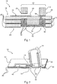
- Fig. 1 shows a portion of a printed circuit board 10 according to the invention for coupling a waveguide 14.
- a microwave conductor 16 is arranged on a printed circuit substrate 12, here on a front side 18.
- the microwave conductor 16 is guided in an interior of the printed circuit board substrate 12. This can have the advantage that contrary to the representation in Fig. 1 no additional separation or shortening of the waveguide 14 for the purpose of isolation at this point is necessary, but the waveguide 14 may have a circumferential plan or flat finish with the advantage of simplified production (for example, cutting).
- the printed circuit board substrate 12 is made of an RF-neutral or for high frequencies in the relevant area insulating material, such as LCP or a PTFE substrate of various manufacturers. Within the printed circuit board substrate 12 a plurality of line levels 20 are arranged to image the corresponding electrical connections of an electronic circuit.
- a connection region 22 describes the region on the front side 18 of the printed circuit substrate 12, which is opposite to the waveguide 14 or where the waveguide 14 is connected to the printed circuit board substrate 12.
- This connection region 22 is annular, so that it can receive a front end 26 of the waveguide 14.
- the connection region 22 is rectangular.
- the connection of likewise rectangular waveguides 14 is possible. It should be noted that various cross-sectional shapes of waveguides 14 and connecting portions 22 are possible, it is useful that the wall of the waveguide 14 and the connecting portion 22 overlap or lie directly opposite each other.
- One end of the microwave conductor 24 protrudes into the connection region 22, so that microwave signals can pass from the microwave conductor 16 or via the end of the microwave conductor 24 into the waveguide 14 and vice versa.
- the end 24 of the microwave conductor 16 acts like a transmitting and receiving antenna that emits and outputs microwave signals into the waveguide 14 can receive the waveguide 14.
- a peripheral recess 30 corresponding to the cross-sectional area of the waveguide 14 is arranged opposite the annular connecting region 22. In the following figures, the spatial configurations of this recess are illustrated.
- a metallic coating 32 is applied, which is shown here as a dashed line.
- other types of coatings or substances are generally possible which have a reflective effect for microwaves in the gigahertz range which is relevant here. This may include, for example, fluids or even gases that have corresponding physical properties or elements such as ions.
- Metallic coatings 32 may be advantageous here, since they can be produced with known methods at relatively low cost and unfold good reflective effect.
- the recess 30 has a width of about 1 mm and a depth and length in the range of less than 1 mm. The dimensions are based on the frequency range of the microwaves used. In one example, a thickness of a metallic coating 32 is about a few microns.
- a lowered portion 34 is surrounded by the recess 30 and forms together with the recess 30 on its side facing the front side 18 a resonator or resonator in cooperation with the waveguide 14.
- the lowered portion 34 can also without lowering according to an example of a metallic coating 32nd respectively.
- the lowering here has the advantage that the resulting space can be potted together with the recess with a synthetic resin 36 and thus a stability of the circuit board 10 can be increased.
- synthetic resin other filling and stabilizing and durable materials such as plastics, adhesives, fillers or the like can be used.
- Through-connections 38 are provided in the printed circuit board substrate 12, which are arranged such that they produce an electrical connection between, for example, a metallic wall of the waveguide 14 and the metallic coating 32 on the rear side 28 of the printed circuit board substrate 12. This can also be achieved, for example, by the plated-through holes contacting a subarea of a line plane 20, which in turn is in electrical contact with the waveguide 14.
- the waveguide 14 may be secured by various mechanisms to the printed circuit board 10 and the printed circuit board substrate 12, for example by soldering, welding or gluing.
- FIG. 2 a circuit board 10 according to the invention with a waveguide 14 is shown in a sectional view.
- a printed circuit board substrate 12 has a plurality of line levels 20.
- a circular encircling recess 30 is introduced on a rear side 28 of the printed circuit board substrate 12.
- a diameter of a lowered region 34 here corresponds approximately to an inner diameter of the waveguide 14.
- the end 24 of a microwave conductor 16 projects into the interior of the waveguide 14 and is thereby guided in isolation from the wall of the waveguide 14.
- a recess may be provided for this purpose.
- the microwave conductor 16 is routed within the printed circuit board substrate, which may eliminate the need for a recess.
- a second recess 40 for receiving an RF chip (not shown) is provided.
- the microwave conductor 16 can advantageously lead into the connection region 22 or the inner region of the waveguide 14. This can be advantageous by a allow adjacent arrangement of high-frequency electronics and thus implement space-saving.
- the second recess 40 may be potted with a synthetic resin to increase mechanical stability and reliability.
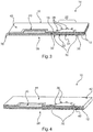
- a further exemplary embodiment of a printed circuit board 10 according to the invention with a printed circuit board substrate 12 and with a plurality of line levels 20 is shown.
- a recess 30 filled with synthetic resin 36 is present on a rear side 28 of the printed circuit board substrate 12, forming a resonator for a hollow conductor (not shown) adjoining the opposite front side 18.
- a microwave conductor 16 extends between a second recess 40 and a connecting region 22.
- Through holes 38 serve to establish an electrical connection between a metallic coating 32 in the recess 30 with the depressed region 34 surrounded by the recess and a connectable waveguide 14 (not shown).
- two adjacent vias 38 are spaced apart less than one quarter of the wavelength of the microwaves. As a result, microwaves can be prevented from escaping between the plated-through holes, thus resulting in unwanted losses.
- Fig. 4 a simplified variant of a printed circuit board 10 according to the invention is shown, with a printed circuit board substrate 12 without line levels 20. This may allow that easily configured and thus inexpensive starting materials for the printed circuit substrate 12 can be used.
- a metallic layer 42 may be applied to a front side 18 of the printed circuit board substrate 12.
- the plated-through holes 38 can be seen, which electrically connect a metallic layer 42 to the front side 18 of the printed circuit board substrate 12.
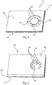
- Fig. 5 shows a simplified example of an inventive Printed circuit board 10, wherein here is a view of a back side 28 of a printed circuit board substrate 12 is shown. Good to see is a circular shaped circumferential recess 30, which includes a lowered portion 34. In this case, plated-through holes 38 are likewise arranged in a circular manner in the recess 30. In the area where a microwave conductor (not shown) is guided on a front side 18 of the printed circuit board substrate 12 in the connection region (not visible here) from the lowered region 34, a larger gap 44 is arranged between the plated through holes 38 for passing through the microwave conductor 16 ,
- a circuit board 10 which has a printed circuit board substrate 12 with a plurality of line levels 20.
- a visible front side 18 of the printed circuit board substrate 12 is surrounded by a plastic 46, which serves as a housing by its stabilizing effect.
- the connection region 22 with plated-through holes 38 and one end of a microwave conductor 24 is recessed in such a way that a tubular waveguide 14 (not shown) can be fastened to the front side 18 of the printed circuit substrate with the plated-through holes 38.
- the circuit board is implemented as a Land Grid Array (LGA).
- LGA Land Grid Array
- the connections of an HF chip can be routed via lines and plated-through holes of bonding pads to the rear side 28 of the printed circuit board substrate 12 and connected there, for example, to soldering pads (not shown).
- a method 100 for generating a resonator for microwaves in a printed circuit board 10 is shown by way of example.
- a provision 110 of a nonconductive planar printed circuit board substrate 12 takes place.
- a ring-shaped recessed hole 30 is produced on a rear side 28 of the printed circuit board substrate 12, in the next step 120. This can be done, for example, by milling or similar methods.
- a coating of microwave-reflecting coating is applied in the latter Recess 30 and on a recessed area 30 enclosed by the region 34 (lowered area) on the back side 28 of the printed circuit board substrate 12.
- the reflective coating is a metallic coating 32nd
- the reflective coating of the recess 30 and the reflective coating of the depressed area 34 on the backside 28 are electrically connected together.
- a vias 38 are made. These run between the front side 18 of the printed circuit board substrate 12 and the reflective coating or metallic layer 42 in the recess 30, wherein the plated-through holes 30 are arranged on the front side 18, that an end face of a waveguide 14 is electrically connected to the vias 38.
- a step 150 of the selective removal of printed circuit board substrate (12) for lowering a region 32 enclosed by the recess 30 in the direction of the front side 18 can take place. This can be done for example by milling.
- the recess 30 and / or the area enclosed by the recess can be coated with a reflective coating in step 160 and stabilized by filling with a synthetic resin. This can be done for example by a via-filling process.
Landscapes
- Engineering & Computer Science (AREA)
- Physics & Mathematics (AREA)
- Radar, Positioning & Navigation (AREA)
- Remote Sensing (AREA)
- General Physics & Mathematics (AREA)
- Electromagnetism (AREA)
- Computer Networks & Wireless Communication (AREA)
- Microelectronics & Electronic Packaging (AREA)
- Thermal Sciences (AREA)
- Fluid Mechanics (AREA)
- Radar Systems Or Details Thereof (AREA)
- Structure Of Printed Boards (AREA)
- Control Of Motors That Do Not Use Commutators (AREA)
- Waveguides (AREA)
Abstract
Description
- Die vorliegende Erfindung betrifft die Messung von Füllständen, beispielsweise in Behältern. Insbesondere betrifft die Erfindung eine Leiterplatte für ein mikrowellenbasiertes oder radarbasiertes Füllstandmessgerät mit einer Einkopplung von Mikrowellen in einen Hohlleiter.
- Bekannte Füllstandmessgeräte nutzen in zunehmendem Maße Prinzipien, die auf der Ausbreitung elektromagnetischer Wellen bzw. ein Reflexionsverhalten und Laufzeitverhalten dieser Wellen zur Bestimmung von Füllständen benutzen. Dabei wird eine hochfrequente elektromagnetische Welle, beispielsweise ein Mikrowellenpuls von einem Füllstandmessgerät in Richtung einer Oberfläche eines Füllgutes in einem Behälter ausgesendet, von dieser Oberfläche reflektiert und auf Basis der Laufzeiten des reflektierten Mikrowellensignals ein Füllstand berechnet. Durch technische Weiterentwicklungen, insbesondere der Elektronik und der Halbleitertechnologie, werden zunehmend auch höhere Frequenzen im oberen zweistelligen Gigahertzbereich zu Füllstandmessungen genutzt. Durch die hohen Frequenzen und die daraus resultierenden physikalischen Eigenschaften der Wellenausbreitung steigen die Anforderungen an insbesondere die Hochfrequenzbauteile solcher Füllstandmessgeräte. Häufig wird hierbei die Hochfrequenzbaugruppe auf einer Leiterplatte realisiert, die die Elektronik für die Erzeugung der Mikrowellenpulse sowie die Antennentechnik beinhaltet.
- Eine Möglichkeit, die erzeugten hochfrequenten Schwingungen weiterzuleiten, beispielsweise an eine externe Antenne, besteht im Anschluss eines Hohlleiters. Diese Hohlleiter sind im verwendeten Frequenzbereich vorteilhaft zum Weiterleiten von Mikrowellensignalen einsetzbar. Eine besondere Herausforderung liegt im Hohlleiterübergang, also der Abstrahlung der elektromagnetischen Welle von einem Leiter (z.B. auf der Leiterplatte) in das Innere eines Hohlleiters und umgekehrt. Dieser Leiter kann beispielsweise als Mikro-Strip ausgeführt sein, dessen Ende in einen Hohlleiter hineinragt. Die Hohlleiter können beispielsweise als Lufthohlleiter ausgeführt sein.
- Um elektrische Verluste und eine gute Anpassung zu erreichen, können hierbei besondere technische Vorkehrungen notwendig sein. So muss beispielsweise der Hohlleiter an seinem Ende zur verlustarmen oder verlustfreien Einkopplung des Signals einen Resonator aufweisen, dessen Größe, Durchmesser und geometrische Ausführung die Verluste im Bereich der verwendeten Frequenzen minimiert. Gleichzeitig ist es wünschenswert, die Größe der Baugruppen zu verkleinern und einen Aufbau bei gleichzeitig hoher Qualität zu vereinfachen. Ein technischer Lösungsansatz kann darin bestehen, die verschiedenen Funktionen möglichst zu integrieren und so einfache und preisgünstige Baugruppen zu erhalten. So ist beispielsweise aus der
EP 1 949 491 B1 ein Hohlleiterübergang bekannt, bei dem der Resonator des Hohlleiters in die Leiterplatte integriert ist. - Ausführungsformen der Erfindung können eine mechanische Stabilität und elektromagnetische Zuverlässigkeit und Genauigkeit eines radarbasierten oder mikrowellenbasierten Füllstandmessgerätes erhöhen. Der im Folgenden beschriebenen Erfindung liegen die folgenden Überlegungen zugrunde: Bei den derzeit bekannten Lösungen wird ein Resonator, der häufig topfförmig ausgestaltet ist, benötigt. Gleichzeitig besteht die Notwendigkeit, diesen Resonator räumlich unmittelbar am Ende des Hohlleiters anzuordnen, um einen verlustfreien oder verlustarmen Abschluss des Hohlleiters zu realisieren. Wird nun der Hohlleiter üblicherweise in einem Winkel von 90° an die Leiterplatte herangeführt, ergibt sich die Notwendigkeit, den Resonator in Richtung eines Substrates der Leiterplatte einzuarbeiten. Im Stand der Technik wird dies beispielsweise dadurch realisiert, dass eine Vertiefung oder Einfräsung in eine Schicht des Leiterplattensubstrates in Verlängerung des Hohlleiters eingebracht wird, die dann, um Verunreinigungen zu vermeiden, meist mit einer Abdeckung aus HF-Substrat oder einem Kunststoffdeckel verschlossen werden muss. Dies kann Nachteile hinsichtlich der elektrischen, elektromagnetischen und mechanischen Eigenschaften der Leiterplatte haben.
- Als Lösung hierfür wird eine Leiterplatte für ein Radar-Füllstandmessgerät vorgeschlagen, die ein nichtleitendes flächiges Leiterplattensubstrat als Trägermaterial aufweist. Neben der Funktion als mechanische Stabilisierung und Trägerfunktion ist das Leiterplattensubstrat isolierend für den verwendeten Frequenzbereich der elektromagnetischen Wellen ausgeführt. Dies kann beispielsweise ein sogenanntes HF-Substrat sein. Auf dem Leiterplattensubstrat ist ein Mikrowellenleiter zur Einkopplung eines Mikrowellensignals in einen Hohlleiter angeordnet. Dies kann beispielsweise als Mikro-Strip-Leiter ausgeführt sein. In einem Beispiel ist dieser auf der Oberfläche des Leiterplattensubstrates angeordnet. In einem weiteren Beispiel verläuft der Mikrowellenleiter zumindest teilweise in einem Inneren des Leiterplattensubstrates.
- Auf einer Vorderseite des Leiterplattensubstrates ist ein umlaufender, also ringförmiger, beispielsweise runder oder eckiger, Verbindungsbereich zur Aufnahme eines stirnseitigen Endes eines Hohlleiters angeordnet. In den meisten Fällen ist das Leiterplattensubstrat beispielsweise als Trägerplatte oder Grundplatte ausgeführt, wobei es sich oft um einen Verbund aus HF-Substrat und einem Grundträger (z.B. FR4) handelt. Durch diese flächige Ausführung kann eine Vorderseite definiert werden, die beispielsweise Bauelemente aufweisen kann. Entsprechend ist eine Rückseite oder Unterseite häufig für Kontaktierungen und Anschlüsse vorgesehen.
- Unter einem ringförmigen Verbindungsbereich ist mit anderen Worten ein Bereich auf der Vorderseite des Leiterplattensubstrates gemeint, der beispielsweise direkt mit dem Hohlleiter, oder auch mit einer Wandung eines Hohlleiters in Berührung kommt oder eine entsprechende mechanische Aufnahme erlaubt. Unter ringförmig ist hier zu verstehen, dass dieser Bereich sich zumindest teilweise in seiner generellen Ausformung an eine Querschnittsform des Hohlleiters anpasst. Ist eine Querschnittsform des Hohlleiters beispielsweise kreisförmig, so ist der Verbindungsbereich ebenfalls in etwa kreisförmig nachgebildet.
- In einem Beispiel ist der Verbindungsbereich rechteckig ausgeführt, um einen Hohlleiter mit rechteckigem Querschnitt aufzunehmen. Der Hohlleiter kann durch entsprechende mechanische Mittel oder auch in Kombination mit elektrischer Kontaktierung mechanisch befestigt werden. Hierzu kann der Hohlleiter am Verbindungsbereich beispielsweise angeklebt, angeschraubt oder angelötet werden.
- Ein Ende des Mikrowellenleiters ragt in den Verbindungsbereich hinein, sodass Mikrowellensignale vom Mikrowellenleiter in den Hohlleiter übergehen können und umgekehrt. In einem Beispiel befindet sich ein Ende des Mikrowellenleiters in etwa in der Mitte des Querschnittes des Hohlleiters. Mit anderen Worten funktioniert das Ende des Mikrowellenleiters wie eine Antenne, die die Mikrowellensignale in den Hohlleiter abstrahlt bzw. von diesem empfängt. In einem Beispiel wird der Mikrowellenleiter innerhalb des Leiterplattensubstrates geführt, wodurch sich die Herstellung einer separaten Aussparung zur isolierten Durchführung des Mikrowellenleiters am Ende des Hohlleiters erübrigen kann.
- Auf einer Rückseite des Leiterplattensubstrates ist gegenüber dem ringförmigen Verbindungsbereich eine, beispielsweise der Querschnittsfläche des Hohlleiters entsprechende und ringförmige, umlaufende Eintiefung in Richtung des Hohlleiters angeordnet. Grundsätzlich kann die Querschnittsfläche des Verbindungsbereichs im Vergleich zur Querschnittsfläche des Hohlleiters einen Sprung machen, da der hintere Bereich mit einem Dielektrikum gefüllt ist und somit kleiner sein könnte.
- Mit anderen Worten verläuft die Eintiefung auf der Rückseite des Leiterplattensubstrates gegenüber dem Bereich, wo eine Wandung des Hohlleiters an die Vorderseite des Leiterplattensubstrates angrenzt. Ziel soll hier sein, einen Abstand zwischen einer Fläche der Rückseite des Leiterplattensubstrates und dem Hohlleiter zu verringern. Dies sollte über einen möglichst großen Bereich der Wandung des Hohlleiters, idealerweise über seinen gesamten Bereich geschehen. Die hierdurch entstehende Struktur bildet in etwa eine topfförmige Form aus, die letztendlich die Form eines Resonators bzw. eines Resonatortopfes bildet. Mit anderen Worten wird hier entgegen den bekannten Lösungen die geometrische Form eines Resonators als negative Formen bzw. invers, also über die Rückseite des Leiterplattensubstrates erzeugt.
- Die Eintiefung muss nicht notwendigerweise eine geschlossene Form aufweisen, sondern es sind auch verschiedenste Formen wie Nute, Kerben, Spalte und Ähnliches denkbar. Auch ist es nicht zwingend notwendig, eine geschlossene Ringform zu implementieren, sondern die Eintiefung kann gemäß einem Beispiel aus mehreren Teilstücken, Teilbögen oder einer Kombination aus verschiedenen Formen bestehen.
- In einem Beispiel ist die Eintiefung als offener Kreisbogen oder auch als offene Rechteckform ausgeführt.
- Der von der Wandung der Eintiefung und ein von der Eintiefung umgebener Bereich der Rückseite des Leiterplattensubstrates weist eine für Mikrowellen reflektierende Beschichtung auf, sodass diese zusammen einen Resonator für die eingekoppelten Mikrowellensignale bilden. Mit anderen Worten wird durch die Eintiefung und den von dieser Eintiefung umgebenen Bereich eine in etwa topfartige Form, also ein so genannter Resonatortopf als elektromagnetischer Abschluss des Hohlleiters, gebildet. Zusammen mit der reflektierenden Beschichtung ergibt sich durch die geometrische Form und die Abmessungen eine Resonanz im relevanten Frequenzbereich. In einem Beispiel sind die Beschichtung in der Eintiefung und die Beschichtung im von der Eintiefung umgebenen Bereich miteinander verbunden. In einem weiteren Beispiel sind die Beschichtung in der Eintiefung und die Beschichtung im umgebenen Bereich voneinander getrennt.
- In einer Ausführungsform der Erfindung ist die reflektierende Beschichtung als metallische Beschichtung ausgeführt. Metallische Beschichtungen können aus verschiedenen Materialien hergestellt werden, vorzugsweise gut leitende Metalle, um den elektromagnetischen und reflektierenden Effekt zu erreichen. Vorteil metallischer Beschichtungen kann eine gute Kontaktierbarkeit und Haltbarkeit sein. In einer weiteren Ausführungsform sind im Bereich der Eintiefung Durchkontaktierungen zwischen der Vorderseite und der metallischen Beschichtung angeordnet, sodass die metallische Beschichtung mit dem Hohlleiter elektrisch verbindbar ist. Mit anderen Worten wird eine elektrische Verbindung zwischen dem Resonatortopf und einer beispielsweise metallisch ausgeführten Wandung des Hohlleiters hergestellt.
- Über die Durchkontaktierungen kann eine elektrische Verbindung auf die jeweils andere Seite des Leiterplattensubstrates geschaffen werden. Dabei kann durch die beispielsweise als elektrisch leitende und metallisierte Bohrung ausgeführten Durchkontaktierungen gleichzeitig die Stabilität des Leiterplattensubstrates erhalten bleiben und gleichzeitig eine ausreichende Güte der elektrischen Verbindung erreicht werden. Auf der Vorderseite kann eine Verbindung zwischen den Durchkontaktierungen und dem Hohlleiter beispielsweise über Schweißverbindungen oder Lötverbindungen hergestellt werden.
- In einer Ausführungsform der Erfindung ist ein Abstand zwischen zwei benachbarten Durchkontaktierungen kleiner als ein Viertel der Wellenlänge der Mikrowellen. Dies kann vorteilhaft eine Ausbreitung der Mikrowellen aus einem Innenbereich des Hohlleiters bzw. einem Innenbereich des Verbindungsbereiches in Bereiche außerhalb des Hohlleiters verhindern. Sozusagen wirken die jeweils benachbart angeordneten Durchkontaktierungen elektromagnetisch insgesamt wie eine durchgängige Sperre für die Mikrowellen.
- In einer Ausführungsform der Erfindung ist der von der Eintiefung eingeschlossene Bereich der Rückseite in Richtung der Vorderseite abgesenkt. Beispielsweise kann dies durch mechanisches Abtragen dieses Bereiches erfolgen. Hierdurch verringert sich ein Abstand dieses Bereiches mit der für Mikrowellen reflektierenden Beschichtung zum Hohlleiter. Durch einen Grad der Absenkung kann beispielsweise eine elektromagnetische Abstimmung des Resonatortopfes auf die verwendeten Frequenzen erfolgen. In einer weiteren Ausführungsform sind die Eintiefung und/oder der von der Eintiefung eingeschlossene Bereich mit einem Kunstharz gefüllt. Dies kann den Vorteil haben, dass durch das Vergießen die ursprüngliche Dicke des Leiterplattensubstrates wiederhergestellt werden kann und somit eine erhöhte mechanische Stabilität des gesamten Leiterplattensubstrates und der Leiterplatte erreicht werden kann. Ohne diese Verfüllung kann der Resonatortopf über die stehenbleibende Leiterplattenschicht mechanisch gehalten werden. Ob dies praktikabel ist, entscheidet beispielsweise das Maß der Eintiefung.
- Das Absenken des Bereiches, der von der Eintiefung umgeben ist, kann so zusätzlich das Aufnehmen einer Schicht aus Kunstharz in dem abgetragenen Bereich ermöglichen und so zusätzliche Stabilität in Verbindung mit dem in der Eintiefung eingebrachten Kunstharz erzeugen. In einem Beispiel erfolgt eine Füllung mit Kunstharz derart, dass eine ursprüngliche plane Oberflächengestalt der Rückseite des Leiterplattensubstrates wieder erzeugt wird.
- In einer Ausführungsform der Erfindung sind der Verbindungsbereich und die Eintiefung rechteckig ausgestaltet. Dies kann den Vorteil haben, dass auch von einem kreisförmigen oder ringförmigen Hohlleiter auf rechteckig ausgestaltete Querschnitte von Hohlleitern zurückgegriffen werden kann. Entsprechend wird in einer weiteren Ausführungsform der Erfindung eine kreisförmige Ausgestaltung dieses Verbindungsbereiches und der Eintiefung vorgeschlagen. Dabei kann gemäß einer weiteren Ausführungsform der Erfindung die Leiterplatte mehrere Leitungsebenen aufweisen, die beispielsweise aus Kupfer hergestellt sein können.
- Gemäß einer weiteren Ausführungsform ist die Leiterplatte als Land Grid Array oder Ball Grid Array ausgeführt. Dies kann beispielsweise bedeuten, dass Kontaktpads auf einer Rückseite des Leiterplattensubstrates zur Kontaktierung mit weiteren Bauteilen und Baugruppen vorgesehen sind. Dies kann weiterhin vorteilhaft eine Ausführung der Leiterplatte in SMD-Bauweise ermöglichen. Gemäß einem Beispiel sind Anschlüsse der Leiterplatte bzw. des Leiterplattensubstrates auf die Rückseite des Leiterplattensubstrates geführt und an Kontaktpads angeschlossen. Diese können beispielsweise über Lötverbindungen weitere Baugruppen verbinden.
- Gemäß einer weiteren Ausführungsform weist die Leiterplatte mehrere Leitungsebenen auf.
- Gemäß einem weiteren Beispiel ist das Leiterplattensubstrat mit einem Kunststoff umgeben. Dieser Kunststoff kann vorteilhaft Funktionen eines Gehäuses abbilden und gleichzeitig Stabilität und geringe Baugröße erreichen. Gemäß einem weiteren Beispiel ist das Leiterplattensubstrat so von dem Kunststoff umgeben, dass der Verbindungsbereich ausgespart ist. Dadurch kann erreicht werden, dass trotz des umgebenden Kunststoffes ein elektrischer Kontakt und mechanischer Kontakt des Hohlleiters mit den Durchkontaktierungen bzw. mit dem Leiterplattensubstrat ermöglicht wird.
- Gemäß einer Ausführungsform der Erfindung weist die Leiterplatte auf der Vorderseite des Leiterplattensubstrates eine zweite Eintiefung zur Aufnahme eines Hochfrequenzchips (HF-Chips) auf, wobei der Mikrowellenleiter zwischen der zweiten Eintiefung und dem Verbindungsbereich verläuft. In dieser zweiten Eintiefung wird der Halbleiterchip platziert und anschließend mit einem sogenannten Glob-Top oder einem Deckel verschlossen.
- Durch das Führen des Mikrowellenleiters auf oder innerhalb des Leiterplattensubstrates bis in den Innenbereich des Hohlleiters ist diese Anordnung gut geeignet, dass Mikrowellensignale von einem HF Chip in einen Hohlleiter zu übertragen.
- Die räumlich beispielsweise in unmittelbarer Nähe des Verbindungsbereiches angeordnete zweite Eintiefung kann somit vorteilhaft bei geringen Verlusten und kompakter mechanischer Implementierung dazu dienen, dass die Leiterplatte gleichzeitig auch die Erzeugung der hochfrequenten elektromagnetischen Signale sowie die Verarbeitung der empfangenen HF-Signale als Funktionseinheit implementieren kann. Dies kann den Vorteil haben, dass die technisch sensiblen Hochfrequenzbauteile kompakt und in sich abgeschlossen in einer Baugruppe vereinigt werden und somit weitestgehend von externen Einflüssen unabhängig sein können. Gemäß einem Beispiel kann der HF Chip auch ohne zweite Eintiefung auf dem Leiterplattensubstrat angeordnet sein. Gemäß einer Ausführungsform der Erfindung ist die zweite Eintiefung mit einem Kunstharz gefüllt. Dies kann vorteilhaft der mechanischen Stabilität sowie dem Schutz vor Umwelteinflüssen dienen.
- Gemäß einem weiteren Aspekt der Erfindung wird ein Verfahren zur Erzeugung eines Resonators für Mikrowellen in einer Leiterplatte vorgestellt. Dieses Verfahren beinhaltet zunächst den Schritt des Bereitstellens eines nichtleitenden flächigen Leiterplattensubstrates. In einem nächsten Schritt wird auf einer Rückseite dieses Leiterplattensubstrates eine ringförmig umlaufende Eintiefung erzeugt. Diese kann gemäß einem Beispiel aus mehreren Teilstücken bestehen, kann aber vorzugsweise auch als geschlossener Ring ausgeführt sein. Danach erfolgt auf einer Wandung der Eintiefung und auf ein von der Eintiefung eingeschlossenen Bereich der Rückseite des Leiterplattensubstrates ein Aufbringen einer für mikrowellenreflektierende Beschichtung. Dies kann beispielsweise eine metallische Schicht sein, wobei im Stand der Technik verschiedene Verfahren zum Aufbringen von metallischen Schichten auf Oberflächen von Leiterplattensubstraten bekannt sind. In einem Beispiel ist nur eine Teilfläche der Wandung und/oder eine Teilfläche des von der Eintiefung eingeschlossenen Bereiches mit einer metallischen oder zumindest reflektierenden Beschichtung versehen.
- In einem weiteren Schritt erfolgt ein Herstellen von Durchkontaktierungen zwischen einer Vorderseite des Leiterplattensubstrates und der reflektierenden Beschichtung in der Eintiefung, wobei die Durchkontaktierungen derart auf der Vorderseite angeordnet sind, dass eine Stirnseite des Hohlleiterendes elektrisch mit den Durchkontaktierungen verbindbar ist. Diese Durchkontaktierungen können beispielsweise als rohrförmige Bohrungen mit anschließender Metallisierung ausgeführt sein. In einer Ausführungsform des Verfahrens beinhaltet das Erzeugen der Eintiefung zusätzlich ein Abtragen von Leiterplattensubstrat zur Absenkung eines von der Eintiefung eingeschlossenen Bereiches in Richtung der Vorderseite.
- Hierdurch kann beispielsweise die letztendliche Form und Dimension des Resonatortopfes, beispielsweise im Zuge einer elektromagnetischen Abstimmung, generiert werden. Dies kann gemäß einem Beispiel auch durch die Anpassung der Form und Größe der Eintiefung auf der Rückseite des Leiterplattensubstrates erfolgen.
- In einer Ausführungsform des erfindungsgemäßen Verfahrens erfolgt das Erzeugen der Eintiefung und/oder des umgebenden Bereiches mittels Fräsen. Dieses Verfahren kann Effizienzvorteile bei gleichzeitig vergleichsweise genauer Erzeugung der gewünschten Formen bei den hier vorherrschenden geringen Abmessungen haben. Gemäß einer weiteren Ausführungsform des erfindungsgemäßen Verfahrens erfolgt ein Auffüllen der Eintiefung und/oder des von der Eintiefung eingeschlossenen Bereiches mit einem Kunstharz. Hierzu kann beispielsweise erwärmtes und flüssiges Kunstharz durch Gießverfahren oder Spritzverfahren, beispielsweise über einen Via-Filling-Prozess, auf das Leiterplattensubstrat aufgetragen werden und so die abgetragenen oder ausgefrästen Bereiche ausgeglichen werden. Vorteil ist hier eine verbesserte Stabilität, da Sollbruchstellen durch dünnere Stellen vermieden werden können und gleichzeitig das Kunstharz eine mechanisch stabile und dauerhafte Verbindung mit dem Leiterplattensubstrat eingehen kann.
- Es ist zu verstehen, dass Merkmale des Verfahrens so wie obenstehend und untenstehend beschrieben auch Merkmale der Leiterplatte sein können und umgekehrt.
- Im Folgenden werden Ausführungsbeispiele der Erfindung mit Bezug auf die beiliegenden Figuren detailliert beschrieben. Weder die Beschreibung noch die Figuren sollen als die Erfindung einschränkend ausgelegt werden.
-
Fig. 1 zeigt einen Teilbereich einer erfindungsgemäßen Leiterplatte in Querschnittsdarstellung. -
Fig. 2 zeigt eine räumliche Schnittdarstellung einer erfindungsgemäßen Leiterplatte mit einem Hohlleiter. -
Fig. 3 zeigt eine Leiterplatte gemäß der Erfindung mit mehreren Leitungsebenen und einer zweiten Eintiefung. -
Fig. 4 zeigt eine Leiterplatte gemäß der Erfindung in vereinfachter Ausführung ohne Leitungsebenen. -
Fig. 5 zeigt eine Rückseite einer erfindungsgemäßen Leiterplatte mit einer kreisförmig umlaufenden Eintiefung und Durchkontaktierungen. -
Fig. 6 zeigt eine Vorderseite einer erfindungsgemäßen Leiterplatte mit einem Kunststoff-Gehäuse und ausgespartem Bereich für einen Hohlleiter. -
Fig. 7 zeigt ein erfindungsgemäßes Verfahren zur Erzeugung eines Resonators für Mikrowellen in einer Leiterplatte. - Die Zeichnungen sind lediglich schematisch und nicht maßstabsgetreu. Grundsätzlich sind identische oder ähnliche Teile mit den gleichen Bezugszeichen versehen.
-
Fig. 1 zeigt einen Teilbereich einer erfindungsgemäßen Leiterplatte 10 zur Ankopplung eines Hohlleiters 14. Auf einem Leiterplattensubstrat 12 ist ein Mikrowellenleiter 16 angeordnet. Im hier gezeigten Beispiel verläuft der Mikrowellenleiter 16 auf einer Oberfläche des Leiterplattensubstrates 12, hier auf einer Vorderseite 18. Gemäß einem (hier nicht gezeigten) Beispiel ist der Mikrowellenleiter 16 in einem Inneren des Leiterplattensubstrates 12 geführt. Dies kann den Vorteil haben, dass entgegen der Darstellung inFig. 1 keine zusätzliche Separierung oder Verkürzung des Hohlleiters 14 zum Zwecke der Isolation an dieser Stelle notwendig ist, sondern der Hohlleiter 14 einen umlaufenden planen bzw. flachen Abschluss mit dem Vorteil vereinfachter Herstellung (zum Beispiel Abschneiden) aufweisen kann. - Das Leiterplattensubstrat 12 ist aus einem HF-neutralen bzw. für Hochfrequenzen im betreffenden Bereich isolierenden Material, beispielsweise LCP oder ein PTFE-Substrat diverser Hersteller, gefertigt. Innerhalb des Leiterplattensubstrates 12 sind mehrere Leitungsebenen 20 angeordnet, um die entsprechenden elektrischen Verbindungen einer Elektronikschaltung abzubilden. Ein Verbindungsbereich 22 beschreibt den Bereich auf der Vorderseite 18 des Leiterplattensubstrates 12, dem der Hohlleiter 14 gegenüberliegt bzw. wo der Hohlleiter 14 mit dem Leiterplattensubstrat 12 verbunden ist. Diese Verbindungsbereich 22 ist ringförmig ausgestaltet, sodass dieser ein stirnseitiges Ende 26 des Hohlleiters 14 aufnehmen kann. Gemäß einem Beispiel ist der Verbindungsbereich 22 rechteckig ausgeführt. Somit ist beispielsweise der Anschluss von ebenfalls rechteckig ausgeführten Hohlleitern 14 möglich. Hierbei ist anzumerken, dass verschiedenste Querschnittsformen von Hohlleitern 14 und Verbindungsbereichen 22 möglich sind, wobei es sinnvoll ist, dass sich die Wandung des Hohlleiters 14 und der Verbindungsbereich 22 überlappen bzw. sich direkt gegenüberliegen.
- Ein Ende des Mikrowellenleiters 24 ragt in den Verbindungsbereich 22 hinein, sodass Mikrowellensignale vom Mikrowellenleiter 16 bzw. über das Ende des Mikrowellenleiters 24 in den Hohlleiter 14 übergehen können und umgekehrt. Mit anderen Worten wirkt das Ende 24 des Mikrowellenleiters 16 wie eine Sende-und Empfangsantenne, die Mikrowellensignale in den Hohlleiter 14 aussendet und aus dem Hohlleiter 14 empfangen kann. Auf einer Rückseite 28 des Leiterplattensubstrates 12 ist gegenüber dem ringförmigen Verbindungsbereich 22 eine der Querschnittsfläche des Hohlleiters 14 entsprechende umlaufende Eintiefung 30 angeordnet. In den folgenden Figuren werden die räumlichen Ausgestaltungen dieser Eintiefung verdeutlicht.
- An einer Wandung der Eintiefung 30 ist eine metallische Beschichtung 32 aufgebracht, die hier als gestrichelte Linie dargestellt ist. Grundsätzlich sind hier neben metallischen Beschichtungen auch andere Arten von Beschichtungen oder Stoffen allgemein möglich, die eine reflektierende Wirkung für Mikrowellen im hier relevanten Gigahertzbereich aufweisen. Hierzu können beispielsweise auch Fluide oder sogar Gase zählen, die entsprechende physikalische Eigenschaften oder Elemente wie beispielsweise Ionen aufweisen. Metallische Beschichtungen 32 können hier vorteilhaft sein, da sie mit bekannten Verfahren zu vergleichsweise geringen Kosten hergestellt werden können und gute reflektierende Wirkung entfalten. In einem Beispiel weist die Eintiefung 30 eine Breite von etwa 1 mm und eine Tiefe und Länge im Bereich von kleiner 1mm auf. Die Abmessungen orientieren sich dabei an dem verwendeten Frequenzbereich der Mikrowellen. Gemäß einem Beispiel beträgt eine Dicke einer metallischen Beschichtung 32 etwa wenige µm.
- Ein abgesenkter Bereich 34 ist von der Eintiefung 30 umgeben und bildet zusammen mit der Eintiefung 30 auf seiner zur Vorderseite 18 gewandten Seite einen Resonator oder Resonatortopf im Zusammenwirken mit dem Hohlleiter 14. Der abgesenkte Bereich 34 kann auch ohne Absenkung gemäß einem Beispiel eine metallische Beschichtung 32 aufweisen. Die Absenkung hat hier den Vorteil, dass der sich ergebende Raum zusammen mit der Eintiefung mit einem Kunstharz 36 vergossen werden kann und so eine Stabilität der Leiterplatte 10 erhöht werden kann. Statt des Kunstharzes sind andere füllende und stabilisierende sowie haltbare Materialien wie Kunststoffe, Klebestoffe, Füllstoffe oder Ähnliches einsetzbar.
- Im Leiterplattensubstrat 12 sind Durchkontaktierungen 38 vorgesehen, die derart angeordnet sind, dass sie eine elektrische Verbindung zwischen beispielsweise einer metallischen Wandung des Hohlleiters 14 und der metallischen Beschichtung 32 auf der Rückseite 28 des Leiterplattensubstrates 12 herstellen. Dies kann beispielsweise auch dadurch geschehen, dass die Durchkontaktierungen einen Teilbereich einer Leitungsebene 20 kontaktieren, die dann ihrerseits in elektrischem Kontakt mit dem Hohlleiter 14 steht. Dabei kann der Hohlleiter 14 durch verschiedene Mechanismen an der Leiterplatte 10 bzw. dem Leiterplattensubstrat 12 befestigt sein, beispielsweise durch Verlöten, Verschweißen oder Verkleben.
- In
Fig. 2 ist eine erfindungsgemäße Leiterplatte 10 mit einem Hohlleiter 14 in einer Schnittdarstellung dargestellt. Ein Leiterplattensubstrat 12 weist mehrere Leitungsebenen 20 auf. Auf einer Rückseite 28 des Leiterplattensubstrates 12 ist eine ringförmig umlaufende Eintiefung 30 eingebracht. Hier ist gut zu erkennen, dass die Eintiefung gegenüber einem stirnseitigen Ende 26 des Hohlleiters 14 auf der Rückseite 28 des Leiterplattensubstrates 12 verläuft. Ein Durchmesser eines abgesenkten Bereiches 34 entspricht hier in etwa einem Innendurchmesser des Hohlleiters 14. Das Ende 24 eines Mikrowellenleiters 16 ragt in das Innere des Hohlleiters 14 und wird dabei isoliert von der Wandung des Hohlleiters 14 geführt. In der Wandung des Hohlleiters 14 kann hierfür beispielsweise eine Aussparung vorgesehen sein. Gemäß einem weiteren Beispiel ist der Mikrowellenleiter 16 innerhalb des Leiterplattensubstrates geführt, was die Notwendigkeit einer Aussparung erübrigen kann. - In einem weiteren Bereich der Vorderseite 18 des Leiterplattensubstrates 12 ist eine zweite Eintiefung 40 zur Aufnahme eines HF-Chips (nicht gezeigt) vorgesehen. Insbesondere durch die inverse oder rückseitige Herstellung des Resonators durch die Eintiefung 30 und die metallische Beschichtung 32 lässt sich der Mikrowellenleiter 16 vorteilhaft in den Verbindungsbereich 22 bzw. den Innenbereich des Hohlleiters 14 führen. Dies kann eben dadurch vorteilhaft eine benachbarte Anordnung einer Hochfrequenzelektronik ermöglichen und so platzsparend implementieren. Die zweite Eintiefung 40 kann mit einem Kunstharz vergossen werden und so mechanische Stabilität und Zuverlässigkeit erhöhen.
- In
Fig. 3 ist eine weitere beispielhafte Ausführungsvariante einer erfindungsgemäßen Leiterplatte 10 mit einem Leiterplattensubstrat 12 und mit mehreren Leitungsebenen 20 gezeigt. Auch in diesem Beispiel ist auf einer Rückseite 28 des Leiterplattensubstrates 12 eine mit Kunstharz 36 ausgefüllte Eintiefung 30 vorhanden, die einen Resonator für einen auf der gegenüberliegenden Vorderseite 18 anschließen Hohlleiter (nicht gezeigt) bildet. Ein Mikrowellenleiter 16 verläuft zwischen einer zweiten Eintiefung 40 und einem Verbindungsbereich 22. Durchkontaktierungen 38 dienen der Herstellung einer elektrischen Verbindung zwischen einer metallischen Beschichtung 32 in der Eintiefung 30 mit dem von der Eintiefung umgebenen abgesenkten Bereich 34 und einem anschließbaren Hohlleiter 14 (nicht gezeigt). In einem Beispiel sind zwei benachbarte Durchkontaktierungen 38 in einem Abstand voneinander angeordnet, der kleiner ist als ein Viertel der Wellenlänge der Mikrowellen. Dadurch kann verhindert werden, dass Mikrowellen zwischen den Durchkontaktierungen austreten und somit ungewollte Verluste auftreten. - In
Fig. 4 ist eine vereinfachte Variante einer erfindungsgemäßen Leiterplatte 10 dargestellt, mit einem Leiterplattensubstrat 12 ohne Leitungsebenen 20. Dies kann erlauben, dass einfach ausgestaltete und somit preiswerte Ausgangsmaterialien für das Leiterplattensubstrat 12 verwendet werden können. Zu Zwecken der Abschirmung kann auf einer Vorderseite 18 des Leiterplattensubstrates 12 eine metallische Schicht 42 aufgetragen sein. Auch hier sind die Durchkontaktierungen 38 zu erkennen, die eine metallische Schicht 42 mit der Vorderseite 18 des Leiterplattensubstrates 12 elektrisch verbinden. -
Fig. 5 zeigt ein vereinfacht dargestelltes Beispiel einer erfindungsgemäßen Leiterplatte 10, wobei hier eine Ansicht einer Rückseite 28 eines Leiterplattensubstrates 12 dargestellt ist. Gut zu erkennen ist eine kreisförmig gestaltete umlaufende Eintiefung 30, die einen abgesenkten Bereich 34 einschließt. Dabei sind Durchkontaktierungen 38 ebenfalls kreisförmig in der Eintiefung 30 angeordnet. In dem Bereich, wo ein Mikrowellenleiter (nicht dargestellt) auf einer Vorderseite 18 des Leiterplattensubstrates 12 in den umseitig vom abgesenkten Bereich 34 befindlichen Verbindungsbereich (hier nicht sichtbar) geführt wird, ist ein größerer Zwischenraum 44 zwischen den Durchkontaktierungen 38 zur Durchführung des Mikrowellenleiters 16 angeordnet. - In
Fig. 6 ist ein Ausführungsbeispiel einer erfindungsgemäßen Leiterplatte 10 gezeigt, die ein Leiterplattensubstrat 12 mit mehreren Leitungsebenen 20 aufweist. Eine hier sichtbare Vorderseite 18 des Leiterplattensubstrates 12 ist mit einem Kunststoff 46 umgeben, dass durch seine stabilisierende Wirkung als Gehäuse dient. Dabei ist der Verbindungsbereich 22 mit Durchkontaktierungen 38 und einem Ende eines Mikrowellenleiters 24 derart ausgespart, dass ein rohrförmiger Hohlleiter 14 (nicht gezeigt) auf der Vorderseite 18 des Leiterplattensubstrates mit den Durchkontaktierungen 38 befestigt werden kann. In einem Beispiel ist die Leiterplatte als Land-Grid-Array (LGA) ausgeführt. Dazu können gemäß einem Beispiel die Anschlüsse eines HF-Chips über Leitungen und Durchkontaktierungen von Bondpads auf die Rückseite 28 des Leiterplattensubstrates 12 geführt sein und dort beispielsweise an Lötpads (nicht gezeigt) angeschlossen werden. - In
Fig. 7 ist ein Verfahren 100 gemäß der Erfindung zur Erzeugung eines Resonators für Mikrowellen in einer Leiterplatte 10 beispielhaft gezeigt. Zunächst erfolgt ein Bereitstellen 110 eines nichtleitenden flächigen Leiterplattensubstrates 12. Auf einer Rückseite 28 des Leiterplattensubstrates 12 erfolgt im nächsten Schritt 120 ein Erzeugen einer ringförmig umlaufenden Eintiefung 30. Dies kann beispielsweise durch Fräsen oder ähnliche Verfahren erfolgen. In einem folgenden Schritt 130 erfolgt ein Aufbringen einer für Mikrowellen reflektierenden Beschichtung in dieser Eintiefung 30 und auf einen von der Eintiefung 30 eingeschlossenen Bereich 34 (abgesenkter Bereich) auf der Rückseite 28 des Leiterplattensubstrates 12. In einem Beispiel ist die reflektierende Beschichtung eine metallische Beschichtung 32. - Gemäß einem Beispiel ist die reflektierende Beschichtung der Eintiefung 30 und die reflektierende Beschichtung des abgesenkten Bereiches 34 auf der Rückseite 28 miteinander elektrisch verbunden. Danach wird in einem Schritt 140 ein Herstellen von Durchkontaktierungen 38 vollzogen. Diese verlaufen zwischen der Vorderseite 18 des Leiterplattensubstrates 12 und der reflektierenden Beschichtung bzw. metallischen Schicht 42 in der Eintiefung 30, wobei die Durchkontaktierungen 30 so auf der Vorderseite 18 angeordnet sind, dass eine Stirnseite eines Hohlleiters 14 elektrisch mit den Durchkontaktierungen 38 verbindbar ist. Optional kann zusätzlich ein Schritt 150 des selektiven Abtragens von Leiterplattensubstrat (12) zur Absenkung eines von der Eintiefung 30 eingeschlossenen Bereiches 32 in Richtung der Vorderseite 18 erfolgen. Dies kann beispielsweise durch Fräsen erfolgen. Die Eintiefung 30 und/oder der von der Eintiefung eingeschlossene Bereich kann im Schritt 160 mit einer reflektierenden Beschichtung überzogen werden und durch Auffüllen mit einem Kunstharz stabilisiert werden. Dies kann beispielsweise durch einen Via-Filling-Prozess erfolgen.
- Ergänzend ist darauf hinzuweisen, dass "umfassend" keine anderen Elemente oder Schritte ausschließt und "eine" oder "ein" keine Vielzahl ausschließt. Ferner sei darauf hingewiesen, dass Merkmale oder Schritte, die mit Verweis auf eines der obigen Ausführungsbeispiele beschrieben worden sind, auch in Kombination mit anderen Merkmalen oder Schritten anderer oben beschriebener Ausführungsbeispiele verwendet werden können. Bezugszeichen in den Ansprüchen sind nicht als Einschränkung anzusehen.
Claims (15)
- Leiterplatte (10) für ein Radar-Füllstandmessgerät, aufweisend- ein nichtleitendes flächiges Leiterplattensubstrat (12);- einen auf dem Leiterplattensubstrat (12) angeordneten Mikrowellenleiter (16) zur Einkopplung eines Mikrowellensignals in einen Hohlleiter (14);wobei auf einer Vorderseite (18) des Leiterplattensubstrates (12) ein umlaufender Verbindungsbereich (22) zur Aufnahme eines stirnseitigen Endes (26) eines Hohlleiters (14) angeordnet ist;
wobei ein Ende des Mikrowellenleiters (24) in den Verbindungbereich (22) hineinragt, sodass Mikrowellensignale vom Mikrowellenleiter (16) in den Hohlleiter (14) übergehen können und umgekehrt;
wobei auf einer Rückseite (28) des Leiterplattensubstrates (12) gegenüber dem Verbindungsbereich (22) eine umlaufende Eintiefung (30) in Richtung des Hohlleiters (14) angeordnet ist;
wobei die Wandung der Eintiefung (30) und ein von der Eintiefung (30) umgebener Bereich (34) der Rückseite (28) des Leiterplattensubstrates (12) eine für Mikrowellen reflektierende Beschichtung (32) aufweisen, sodass diese zusammen einen Resonator für die eingekoppelten Mikrowellensignale bilden. - Leiterplatte (10) gemäß Anspruch 1, wobei die reflektierende Beschichtung (32) als metallische Beschichtung ausgeführt ist.
- Leiterplatte (10) gemäß einem der Ansprüche 1 oder 2, wobei im Bereich der Eintiefung Durchkontaktierungen (38) zwischen der Vorderseite (18) und der metallischen Beschichtung (32) angeordnet sind, sodass die metallische Beschichtung (32) mit dem Hohlleiter (14) elektrisch verbindbar ist.
- Leiterplatte (10) gemäß Anspruch 3, wobei ein Abstand zwischen zwei benachbarten Durchkontaktierungen (38) kleiner als ein Viertel der Wellenlänge der Mikrowellen ist.
- Leiterplatte (10) gemäß einem der vorhergehenden Ansprüche, wobei der von der Eintiefung (30) eingeschlossene Bereich der Rückseite (28) in Richtung der Vorderseite (18) abgesenkt ist.
- Leiterplatte (10) gemäß einem der vorhergehenden Ansprüche, wobei die Eintiefung (30) und/oder der von der Eintiefung (30) eingeschlossene Bereich mit einem anderen Material aufgefüllt ist.
- Leiterplatte (10) gemäß einem der vorhergehenden Ansprüche, wobei der Verbindungsbereich und die Eintiefung kreisförmig ausgestaltet sind.
- Leiterplatte (10) gemäß einem der vorhergehenden Ansprüche, wobei der Verbindungsbereich (22) und die Eintiefung (30) eine rechteckige Form aufweisen.
- Leiterplatte (10) gemäß einem der vorhergehenden Ansprüche, wobei die Leiterplatte (10) auf der Vorderseite des Leiterplattensubstrates (12) eine zweite Eintiefung (40) zur Aufnahme eines HF-Chips aufweist und der Mikrowellenleiter (16) zwischen der zweiten Eintiefung (30) und dem Verbindungsbereich (22) verläuft.
- Leiterplatte (10) gemäß Anspruch 9, wobei die zweite Eintiefung (40) mit einem Kunstharz gefüllt ist.
- Radarfüllstandmessgerät mit einer Leiterplatte (10) gemäß einem der Ansprüche 1 bis 10.
- Verfahren (100) zur Erzeugung eines Resonators für Mikrowellen in einer Leiterplatte (10), aufweisend die Schritte:- Bereitstellen (110) eines nichtleitenden flächigen Leiterplattensubstrates (12);- Erzeugen (120) einer umlaufenden Eintiefung (30) auf einer Rückseite (28) des Leiterplattensubstrates (12);- Aufbringen (130) einer für Mikrowellen reflektierenden Beschichtung (32) auf eine Wandung der Eintiefung (30) und auf einen von der Eintiefung (30) eingeschlossenen Bereich (34) der Rückseite (28) des Leiterplattensubstrates (12);- Herstellen (140) von Durchkontaktierungen (38) zwischen einer Vorderseite (18) des Leiterplattensubstrates (12) und der reflektierenden Beschichtung (32) in der Eintiefung, wobei die Durchkontaktierungen (38) derart auf der Vorderseite (18) angeordnet sind, dass eine Stirnseite eines Hohlleiterendes (26) elektrisch mit den Durchkontaktierungen (38) verbindbar ist.
- Verfahren (100) gemäß Anspruch 12, wobei das Erzeugen (120) der Eintiefung (30) zusätzlich ein Abtragen (150) von Leiterplattensubstrat (12) zur Absenkung eines von der Eintiefung (30) eingeschlossenen Bereiches (34) in Richtung der Vorderseite (18) beinhaltet.
- Verfahren (100) gemäß Anspruch 12 oder 13, wobei das Erzeugen (120) der Eintiefung (30) und/oder des umgebenen Bereiches (34) mittels Fräsen oder mittels Laser erfolgt.
- Verfahren (100) gemäß einem der Ansprüche 12 bis 14, weiterhin aufweisend den Schritt:- Auffüllen (160) der Eintiefung (30) und/oder des von der Eintiefung (30) eingeschlossenen Bereiches (34) mit einem anderen Material.
Priority Applications (8)
| Application Number | Priority Date | Filing Date | Title |
|---|---|---|---|
| HUE17205156A HUE049220T2 (hu) | 2017-12-04 | 2017-12-04 | Nyomtatott áramköri lap radaros feltöltési szintmérõ készülékhez üreges vezetõ becsatolással |
| EP17205156.7A EP3492881B1 (de) | 2017-12-04 | 2017-12-04 | Leiterplatte für ein radar-füllstandmessgerät mit hohlleitereinkopplung |
| ES17205156T ES2792043T3 (es) | 2017-12-04 | 2017-12-04 | Placa de circuitos impresos para un aparato de medición de nivel de llenado por radar con un acoplamiento de guía de ondas |
| TW107141369A TWI811264B (zh) | 2017-12-04 | 2018-11-21 | 用於具有波導耦合裝置之雷達物位量測裝置的電路板 |
| CN201811405763.9A CN110006504B (zh) | 2017-12-04 | 2018-11-23 | 用于具有波导耦合装置的雷达物位测量装置的电路板 |
| KR1020180150225A KR102443998B1 (ko) | 2017-12-04 | 2018-11-28 | 도파관 결합을 갖는 레이더 레벨 측정 장치용 인쇄 회로 기판 |
| RU2018142537A RU2760235C2 (ru) | 2017-12-04 | 2018-12-03 | Печатная плата для радиолокационного устройства измерения уровня заполнения с волноводным вводом |
| US16/209,761 US10616996B2 (en) | 2017-12-04 | 2018-12-04 | Printed circuit board for a radar level measurement device with waveguide coupling |
Applications Claiming Priority (1)
| Application Number | Priority Date | Filing Date | Title |
|---|---|---|---|
| EP17205156.7A EP3492881B1 (de) | 2017-12-04 | 2017-12-04 | Leiterplatte für ein radar-füllstandmessgerät mit hohlleitereinkopplung |
Publications (2)
| Publication Number | Publication Date |
|---|---|
| EP3492881A1 true EP3492881A1 (de) | 2019-06-05 |
| EP3492881B1 EP3492881B1 (de) | 2020-02-26 |
Family
ID=60569797
Family Applications (1)
| Application Number | Title | Priority Date | Filing Date |
|---|---|---|---|
| EP17205156.7A Active EP3492881B1 (de) | 2017-12-04 | 2017-12-04 | Leiterplatte für ein radar-füllstandmessgerät mit hohlleitereinkopplung |
Country Status (8)
| Country | Link |
|---|---|
| US (1) | US10616996B2 (de) |
| EP (1) | EP3492881B1 (de) |
| KR (1) | KR102443998B1 (de) |
| CN (1) | CN110006504B (de) |
| ES (1) | ES2792043T3 (de) |
| HU (1) | HUE049220T2 (de) |
| RU (1) | RU2760235C2 (de) |
| TW (1) | TWI811264B (de) |
Cited By (2)
| Publication number | Priority date | Publication date | Assignee | Title |
|---|---|---|---|---|
| DE102019217735A1 (de) * | 2019-11-18 | 2021-05-20 | Vega Grieshaber Kg | Radarchip mit einer Hohlleitereinkopplung |
| DE102019217736A1 (de) * | 2019-11-18 | 2021-05-20 | Vega Grieshaber Kg | Radarchip mit einer Hohlleitereinkopplung |
Families Citing this family (11)
| Publication number | Priority date | Publication date | Assignee | Title |
|---|---|---|---|---|
| DE102018132285A1 (de) * | 2018-12-14 | 2020-06-18 | Endress+Hauser SE+Co. KG | Füllstandsmessgerät |
| CN111982240B (zh) * | 2020-09-30 | 2023-04-25 | 北京古大仪表有限公司 | 一种雷达物位计 |
| US11757166B2 (en) * | 2020-11-10 | 2023-09-12 | Aptiv Technologies Limited | Surface-mount waveguide for vertical transitions of a printed circuit board |
| CN112467326B (zh) * | 2020-12-07 | 2021-10-01 | 之江实验室 | 一种宽带矩形波导-微带转换器 |
| DE102020216362A1 (de) * | 2020-12-21 | 2022-06-23 | Robert Bosch Gesellschaft mit beschränkter Haftung | Verfahren zur Herstellung eines Radarsensors |
| HU231635B1 (hu) * | 2022-04-13 | 2025-04-28 | Nivelco Ipari Elektronika Zrt. | Körpolarizált antenna csatoló szerkezet |
| TWI823434B (zh) * | 2022-06-22 | 2023-11-21 | 先豐通訊股份有限公司 | 波導電路板及其製造方法 |
| US11885842B1 (en) * | 2022-09-13 | 2024-01-30 | Quantum Valley Ideas Laboratories | Controlling electric fields in vapor cells |
| US11899051B1 (en) * | 2022-09-13 | 2024-02-13 | Quantum Valley Ideas Laboratories | Controlling electric fields in vapor cells having a body defined by a stack of layers |
| CN120033431A (zh) * | 2023-11-21 | 2025-05-23 | 中兴通讯股份有限公司 | 波导通信装置及其制作方法 |
| CN119340635B (zh) * | 2024-12-19 | 2025-06-27 | 健鼎(无锡)电子有限公司 | 一种波导雷达基板制造方法 |
Citations (3)
| Publication number | Priority date | Publication date | Assignee | Title |
|---|---|---|---|---|
| EP1949491B1 (de) | 2005-11-14 | 2011-07-06 | VEGA Grieshaber KG | Hohlleiterübergang |
| DE112010003585T5 (de) * | 2009-09-08 | 2012-11-22 | Siklu Communication ltd. | Rfic-schnittstellen und millimeterwellenstrukturen |
| DE102015119690A1 (de) * | 2015-11-13 | 2017-05-18 | Endress + Hauser Gmbh + Co. Kg | Radarbasierter Füllstandsensor |
Family Cites Families (12)
| Publication number | Priority date | Publication date | Assignee | Title |
|---|---|---|---|---|
| FR2700066A1 (fr) * | 1992-12-29 | 1994-07-01 | Philips Electronique Lab | Dispositif hyperfréquences comprenant au moins une transition entre une ligne de transmission intégrée sur un substrat et un guide d'onde. |
| JP2605654B2 (ja) * | 1995-03-31 | 1997-04-30 | 日本電気株式会社 | 複合マイクロ波回路モジュール及びその製造方法 |
| US5914684A (en) * | 1997-04-18 | 1999-06-22 | Honeywell Inc. | Electromagnetic transducer system with integrated circuit card adapter |
| CN1274056C (zh) * | 2000-10-18 | 2006-09-06 | 诺基亚公司 | 波导到带状线转接 |
| DE10065624C2 (de) * | 2000-12-29 | 2002-11-14 | Hans Kragl | Kopplungsanordnung zum optischen Koppeln eines Lichtwellenleiters mit einem elektro-optischen oder opto-elektrischen Halbleiterwandler |
| KR100891694B1 (ko) * | 2002-11-20 | 2009-04-03 | 로즈마운트 탱크 레이더 에이비 | 레이더 기반의 레벨 측정장치 및 방법 |
| US7720116B2 (en) * | 2004-01-22 | 2010-05-18 | Vescent Photonics, Inc. | Tunable laser having liquid crystal waveguide |
| US7791278B2 (en) * | 2005-10-27 | 2010-09-07 | Luxim Corporation | High brightness plasma lamp |
| DE102005054233A1 (de) * | 2005-11-14 | 2007-05-16 | Grieshaber Vega Kg | Hohlleiterübergang |
| US8730093B2 (en) * | 2011-09-27 | 2014-05-20 | Rosemount Tank Radar Ab | MFPW radar level gauging with distance approximation |
| US9212942B2 (en) * | 2012-07-04 | 2015-12-15 | Vega Grieshaber Kg | Waveguide coupling, high-frequency module, fill-level radar and use |
| CN103700947B (zh) * | 2013-12-30 | 2016-08-17 | 电子科技大学 | 基片集成波导圆极化天线 |
-
2017
- 2017-12-04 EP EP17205156.7A patent/EP3492881B1/de active Active
- 2017-12-04 ES ES17205156T patent/ES2792043T3/es active Active
- 2017-12-04 HU HUE17205156A patent/HUE049220T2/hu unknown
-
2018
- 2018-11-21 TW TW107141369A patent/TWI811264B/zh active
- 2018-11-23 CN CN201811405763.9A patent/CN110006504B/zh active Active
- 2018-11-28 KR KR1020180150225A patent/KR102443998B1/ko active Active
- 2018-12-03 RU RU2018142537A patent/RU2760235C2/ru active
- 2018-12-04 US US16/209,761 patent/US10616996B2/en active Active
Patent Citations (3)
| Publication number | Priority date | Publication date | Assignee | Title |
|---|---|---|---|---|
| EP1949491B1 (de) | 2005-11-14 | 2011-07-06 | VEGA Grieshaber KG | Hohlleiterübergang |
| DE112010003585T5 (de) * | 2009-09-08 | 2012-11-22 | Siklu Communication ltd. | Rfic-schnittstellen und millimeterwellenstrukturen |
| DE102015119690A1 (de) * | 2015-11-13 | 2017-05-18 | Endress + Hauser Gmbh + Co. Kg | Radarbasierter Füllstandsensor |
Cited By (3)
| Publication number | Priority date | Publication date | Assignee | Title |
|---|---|---|---|---|
| DE102019217735A1 (de) * | 2019-11-18 | 2021-05-20 | Vega Grieshaber Kg | Radarchip mit einer Hohlleitereinkopplung |
| DE102019217736A1 (de) * | 2019-11-18 | 2021-05-20 | Vega Grieshaber Kg | Radarchip mit einer Hohlleitereinkopplung |
| US12241992B2 (en) | 2019-11-18 | 2025-03-04 | Vega Grieshaber Kg | Radar chip with a waveguide coupling |
Also Published As
| Publication number | Publication date |
|---|---|
| EP3492881B1 (de) | 2020-02-26 |
| TWI811264B (zh) | 2023-08-11 |
| CN110006504A (zh) | 2019-07-12 |
| RU2018142537A (ru) | 2020-06-03 |
| RU2018142537A3 (de) | 2021-09-27 |
| TW201937996A (zh) | 2019-09-16 |
| US20190191545A1 (en) | 2019-06-20 |
| US10616996B2 (en) | 2020-04-07 |
| KR20190065945A (ko) | 2019-06-12 |
| RU2760235C2 (ru) | 2021-11-23 |
| HUE049220T2 (hu) | 2020-09-28 |
| ES2792043T3 (es) | 2020-11-06 |
| KR102443998B1 (ko) | 2022-09-16 |
| CN110006504B (zh) | 2022-06-07 |
Similar Documents
| Publication | Publication Date | Title |
|---|---|---|
| EP3492881B1 (de) | Leiterplatte für ein radar-füllstandmessgerät mit hohlleitereinkopplung | |
| DE112013001709B4 (de) | Elektronische Halbleiterbaugruppe für Millimeterwellen-Halbleiterplättchen | |
| DE60214755T2 (de) | Hornantenne für eine Pegelmesseinrichtung | |
| DE102016120665B3 (de) | Radarsensoreinheit zum Einsatz in rauen Umgebungen | |
| DE10323431B4 (de) | Hochfrequenzzuleitungs-Wellenleiter-Umsetzer | |
| EP1083413B1 (de) | Vorrichtung zur Bestimmung des Füllstands eines Füllguts in einem Behälter | |
| WO2014006150A1 (de) | Hohlleitereinkopplung, hochfrequenzmodul, füllstandradar und verwendung | |
| EP3450931B1 (de) | Hohlleitereinkopplung für ein füllstandradar | |
| EP3824258B1 (de) | Hochfrequenzbaustein | |
| EP3830894B1 (de) | Hochfrequenzbaustein | |
| EP3696516B1 (de) | Radarmodul | |
| EP4047742B1 (de) | Radarmodul | |
| EP2963440A1 (de) | Mikrowellenmodul | |
| WO2021099122A1 (de) | Radarchip mit einer hohlleitereinkopplung | |
| EP3903376B1 (de) | Hohlleiteranordnung | |
| EP2683022B1 (de) | Gasdichte Hohlleitereinkopplung, Hochfrequenzmodul, Füllstandradar und Verwendung | |
| DE102006019054B4 (de) | Hochfrequenzanordnung mit einem Übergang zwischen einem Hohlleiter und einer Mikrostrip-Leitung | |
| WO2014090565A1 (de) | Füllstandsmessgerät | |
| DE102017203832B3 (de) | Gehäuse für einen Hochfrequenzchip | |
| DE112014001166B4 (de) | Optoelektronisches Bauelement und elektronisches Gerät mit optoelektronischem Bauelement | |
| DE102017203823A1 (de) | Hochfrequenz-Radarmodul für ein Füllstandradar | |
| EP3259801B1 (de) | Vorrichtung und verfahren zum übertragen eines hochfrequenzsignals | |
| WO2001003243A1 (de) | Baugruppe mit einer antenne | |
| DE102005056756A1 (de) | Antennenanordnung für einen Radar-Sensor | |
| DE102023131661B4 (de) | Baugruppe für Hochfrequenzfeldgeräte, Hochfrequenzfeldgerät und Messstelle |
Legal Events
| Date | Code | Title | Description |
|---|---|---|---|
| PUAI | Public reference made under article 153(3) epc to a published international application that has entered the european phase |
Free format text: ORIGINAL CODE: 0009012 |
|
| STAA | Information on the status of an ep patent application or granted ep patent |
Free format text: STATUS: REQUEST FOR EXAMINATION WAS MADE |
|
| 17P | Request for examination filed |
Effective date: 20180920 |
|
| AK | Designated contracting states |
Kind code of ref document: A1 Designated state(s): AL AT BE BG CH CY CZ DE DK EE ES FI FR GB GR HR HU IE IS IT LI LT LU LV MC MK MT NL NO PL PT RO RS SE SI SK SM TR |
|
| AX | Request for extension of the european patent |
Extension state: BA ME |
|
| REG | Reference to a national code |
Ref country code: DE Ref legal event code: R079 Ref document number: 502017003958 Country of ref document: DE Free format text: PREVIOUS MAIN CLASS: G01F0023284000 Ipc: G01S0007030000 |
|
| GRAP | Despatch of communication of intention to grant a patent |
Free format text: ORIGINAL CODE: EPIDOSNIGR1 |
|
| STAA | Information on the status of an ep patent application or granted ep patent |
Free format text: STATUS: GRANT OF PATENT IS INTENDED |
|
| RIC1 | Information provided on ipc code assigned before grant |
Ipc: G01S 7/02 20060101ALI20190916BHEP Ipc: G01F 23/284 20060101ALI20190916BHEP Ipc: G01S 13/88 20060101ALI20190916BHEP Ipc: G01S 7/03 20060101AFI20190916BHEP Ipc: H01P 5/107 20060101ALI20190916BHEP |
|
| INTG | Intention to grant announced |
Effective date: 20191022 |
|
| GRAS | Grant fee paid |
Free format text: ORIGINAL CODE: EPIDOSNIGR3 |
|
| GRAA | (expected) grant |
Free format text: ORIGINAL CODE: 0009210 |
|
| STAA | Information on the status of an ep patent application or granted ep patent |
Free format text: STATUS: THE PATENT HAS BEEN GRANTED |
|
| AK | Designated contracting states |
Kind code of ref document: B1 Designated state(s): AL AT BE BG CH CY CZ DE DK EE ES FI FR GB GR HR HU IE IS IT LI LT LU LV MC MK MT NL NO PL PT RO RS SE SI SK SM TR |
|
| REG | Reference to a national code |
Ref country code: GB Ref legal event code: FG4D Free format text: NOT ENGLISH |
|
| REG | Reference to a national code |
Ref country code: CH Ref legal event code: EP |
|
| REG | Reference to a national code |
Ref country code: DE Ref legal event code: R096 Ref document number: 502017003958 Country of ref document: DE |
|
| REG | Reference to a national code |
Ref country code: AT Ref legal event code: REF Ref document number: 1238318 Country of ref document: AT Kind code of ref document: T Effective date: 20200315 |
|
| REG | Reference to a national code |
Ref country code: IE Ref legal event code: FG4D Free format text: LANGUAGE OF EP DOCUMENT: GERMAN |
|
| REG | Reference to a national code |
Ref country code: NL Ref legal event code: FP |
|
| REG | Reference to a national code |
Ref country code: SE Ref legal event code: TRGR |
|
| PG25 | Lapsed in a contracting state [announced via postgrant information from national office to epo] |
Ref country code: FI Free format text: LAPSE BECAUSE OF FAILURE TO SUBMIT A TRANSLATION OF THE DESCRIPTION OR TO PAY THE FEE WITHIN THE PRESCRIBED TIME-LIMIT Effective date: 20200226 Ref country code: RS Free format text: LAPSE BECAUSE OF FAILURE TO SUBMIT A TRANSLATION OF THE DESCRIPTION OR TO PAY THE FEE WITHIN THE PRESCRIBED TIME-LIMIT Effective date: 20200226 Ref country code: NO Free format text: LAPSE BECAUSE OF FAILURE TO SUBMIT A TRANSLATION OF THE DESCRIPTION OR TO PAY THE FEE WITHIN THE PRESCRIBED TIME-LIMIT Effective date: 20200526 |
|
| REG | Reference to a national code |
Ref country code: LT Ref legal event code: MG4D |
|
| PG25 | Lapsed in a contracting state [announced via postgrant information from national office to epo] |
Ref country code: BG Free format text: LAPSE BECAUSE OF FAILURE TO SUBMIT A TRANSLATION OF THE DESCRIPTION OR TO PAY THE FEE WITHIN THE PRESCRIBED TIME-LIMIT Effective date: 20200526 Ref country code: IS Free format text: LAPSE BECAUSE OF FAILURE TO SUBMIT A TRANSLATION OF THE DESCRIPTION OR TO PAY THE FEE WITHIN THE PRESCRIBED TIME-LIMIT Effective date: 20200626 Ref country code: GR Free format text: LAPSE BECAUSE OF FAILURE TO SUBMIT A TRANSLATION OF THE DESCRIPTION OR TO PAY THE FEE WITHIN THE PRESCRIBED TIME-LIMIT Effective date: 20200527 Ref country code: LV Free format text: LAPSE BECAUSE OF FAILURE TO SUBMIT A TRANSLATION OF THE DESCRIPTION OR TO PAY THE FEE WITHIN THE PRESCRIBED TIME-LIMIT Effective date: 20200226 Ref country code: HR Free format text: LAPSE BECAUSE OF FAILURE TO SUBMIT A TRANSLATION OF THE DESCRIPTION OR TO PAY THE FEE WITHIN THE PRESCRIBED TIME-LIMIT Effective date: 20200226 |
|
| REG | Reference to a national code |
Ref country code: HU Ref legal event code: AG4A Ref document number: E049220 Country of ref document: HU |
|
| PG25 | Lapsed in a contracting state [announced via postgrant information from national office to epo] |
Ref country code: SK Free format text: LAPSE BECAUSE OF FAILURE TO SUBMIT A TRANSLATION OF THE DESCRIPTION OR TO PAY THE FEE WITHIN THE PRESCRIBED TIME-LIMIT Effective date: 20200226 Ref country code: PT Free format text: LAPSE BECAUSE OF FAILURE TO SUBMIT A TRANSLATION OF THE DESCRIPTION OR TO PAY THE FEE WITHIN THE PRESCRIBED TIME-LIMIT Effective date: 20200719 Ref country code: LT Free format text: LAPSE BECAUSE OF FAILURE TO SUBMIT A TRANSLATION OF THE DESCRIPTION OR TO PAY THE FEE WITHIN THE PRESCRIBED TIME-LIMIT Effective date: 20200226 Ref country code: DK Free format text: LAPSE BECAUSE OF FAILURE TO SUBMIT A TRANSLATION OF THE DESCRIPTION OR TO PAY THE FEE WITHIN THE PRESCRIBED TIME-LIMIT Effective date: 20200226 Ref country code: EE Free format text: LAPSE BECAUSE OF FAILURE TO SUBMIT A TRANSLATION OF THE DESCRIPTION OR TO PAY THE FEE WITHIN THE PRESCRIBED TIME-LIMIT Effective date: 20200226 Ref country code: SM Free format text: LAPSE BECAUSE OF FAILURE TO SUBMIT A TRANSLATION OF THE DESCRIPTION OR TO PAY THE FEE WITHIN THE PRESCRIBED TIME-LIMIT Effective date: 20200226 Ref country code: CZ Free format text: LAPSE BECAUSE OF FAILURE TO SUBMIT A TRANSLATION OF THE DESCRIPTION OR TO PAY THE FEE WITHIN THE PRESCRIBED TIME-LIMIT Effective date: 20200226 Ref country code: RO Free format text: LAPSE BECAUSE OF FAILURE TO SUBMIT A TRANSLATION OF THE DESCRIPTION OR TO PAY THE FEE WITHIN THE PRESCRIBED TIME-LIMIT Effective date: 20200226 |
|
| REG | Reference to a national code |
Ref country code: ES Ref legal event code: FG2A Ref document number: 2792043 Country of ref document: ES Kind code of ref document: T3 Effective date: 20201106 |
|
| REG | Reference to a national code |
Ref country code: DE Ref legal event code: R097 Ref document number: 502017003958 Country of ref document: DE |
|
| PLBE | No opposition filed within time limit |
Free format text: ORIGINAL CODE: 0009261 |
|
| STAA | Information on the status of an ep patent application or granted ep patent |
Free format text: STATUS: NO OPPOSITION FILED WITHIN TIME LIMIT |
|
| 26N | No opposition filed |
Effective date: 20201127 |
|
| PG25 | Lapsed in a contracting state [announced via postgrant information from national office to epo] |
Ref country code: PL Free format text: LAPSE BECAUSE OF FAILURE TO SUBMIT A TRANSLATION OF THE DESCRIPTION OR TO PAY THE FEE WITHIN THE PRESCRIBED TIME-LIMIT Effective date: 20200226 |
|
| REG | Reference to a national code |
Ref country code: CH Ref legal event code: PL |
|
| PG25 | Lapsed in a contracting state [announced via postgrant information from national office to epo] |
Ref country code: MC Free format text: LAPSE BECAUSE OF FAILURE TO SUBMIT A TRANSLATION OF THE DESCRIPTION OR TO PAY THE FEE WITHIN THE PRESCRIBED TIME-LIMIT Effective date: 20200226 |
|
| REG | Reference to a national code |
Ref country code: BE Ref legal event code: MM Effective date: 20201231 |
|
| PG25 | Lapsed in a contracting state [announced via postgrant information from national office to epo] |
Ref country code: LU Free format text: LAPSE BECAUSE OF NON-PAYMENT OF DUE FEES Effective date: 20201204 Ref country code: IE Free format text: LAPSE BECAUSE OF NON-PAYMENT OF DUE FEES Effective date: 20201204 |
|
| PG25 | Lapsed in a contracting state [announced via postgrant information from national office to epo] |
Ref country code: CH Free format text: LAPSE BECAUSE OF NON-PAYMENT OF DUE FEES Effective date: 20201231 Ref country code: LI Free format text: LAPSE BECAUSE OF NON-PAYMENT OF DUE FEES Effective date: 20201231 |
|
| PG25 | Lapsed in a contracting state [announced via postgrant information from national office to epo] |
Ref country code: TR Free format text: LAPSE BECAUSE OF FAILURE TO SUBMIT A TRANSLATION OF THE DESCRIPTION OR TO PAY THE FEE WITHIN THE PRESCRIBED TIME-LIMIT Effective date: 20200226 Ref country code: MT Free format text: LAPSE BECAUSE OF FAILURE TO SUBMIT A TRANSLATION OF THE DESCRIPTION OR TO PAY THE FEE WITHIN THE PRESCRIBED TIME-LIMIT Effective date: 20200226 Ref country code: CY Free format text: LAPSE BECAUSE OF FAILURE TO SUBMIT A TRANSLATION OF THE DESCRIPTION OR TO PAY THE FEE WITHIN THE PRESCRIBED TIME-LIMIT Effective date: 20200226 |
|
| PG25 | Lapsed in a contracting state [announced via postgrant information from national office to epo] |
Ref country code: MK Free format text: LAPSE BECAUSE OF FAILURE TO SUBMIT A TRANSLATION OF THE DESCRIPTION OR TO PAY THE FEE WITHIN THE PRESCRIBED TIME-LIMIT Effective date: 20200226 Ref country code: AL Free format text: LAPSE BECAUSE OF FAILURE TO SUBMIT A TRANSLATION OF THE DESCRIPTION OR TO PAY THE FEE WITHIN THE PRESCRIBED TIME-LIMIT Effective date: 20200226 |
|
| PG25 | Lapsed in a contracting state [announced via postgrant information from national office to epo] |
Ref country code: BE Free format text: LAPSE BECAUSE OF NON-PAYMENT OF DUE FEES Effective date: 20201231 |
|
| P01 | Opt-out of the competence of the unified patent court (upc) registered |
Effective date: 20230508 |
|
| PG25 | Lapsed in a contracting state [announced via postgrant information from national office to epo] |
Ref country code: SI Free format text: LAPSE BECAUSE OF FAILURE TO SUBMIT A TRANSLATION OF THE DESCRIPTION OR TO PAY THE FEE WITHIN THE PRESCRIBED TIME-LIMIT Effective date: 20200226 |
|
| REG | Reference to a national code |
Ref country code: AT Ref legal event code: MM01 Ref document number: 1238318 Country of ref document: AT Kind code of ref document: T Effective date: 20221204 |
|
| PG25 | Lapsed in a contracting state [announced via postgrant information from national office to epo] |
Ref country code: AT Free format text: LAPSE BECAUSE OF NON-PAYMENT OF DUE FEES Effective date: 20221204 |
|
| PG25 | Lapsed in a contracting state [announced via postgrant information from national office to epo] |
Ref country code: AT Free format text: LAPSE BECAUSE OF NON-PAYMENT OF DUE FEES Effective date: 20221204 |
|
| PGFP | Annual fee paid to national office [announced via postgrant information from national office to epo] |
Ref country code: GB Payment date: 20251218 Year of fee payment: 9 |
|
| PGFP | Annual fee paid to national office [announced via postgrant information from national office to epo] |
Ref country code: HU Payment date: 20251202 Year of fee payment: 9 Ref country code: NL Payment date: 20251217 Year of fee payment: 9 Ref country code: FR Payment date: 20251218 Year of fee payment: 9 |
|
| PGFP | Annual fee paid to national office [announced via postgrant information from national office to epo] |
Ref country code: SE Payment date: 20251217 Year of fee payment: 9 |
|
| PGFP | Annual fee paid to national office [announced via postgrant information from national office to epo] |
Ref country code: ES Payment date: 20260119 Year of fee payment: 9 |
|
| PGFP | Annual fee paid to national office [announced via postgrant information from national office to epo] |
Ref country code: DE Payment date: 20251222 Year of fee payment: 9 |
|
| PGFP | Annual fee paid to national office [announced via postgrant information from national office to epo] |
Ref country code: AT Payment date: 20260410 Year of fee payment: 5 |
|
| PGFP | Annual fee paid to national office [announced via postgrant information from national office to epo] |
Ref country code: IT Payment date: 20251231 Year of fee payment: 9 |