EP3490148A2 - Capacitance detecting device - Google Patents
Capacitance detecting device Download PDFInfo
- Publication number
- EP3490148A2 EP3490148A2 EP18208922.7A EP18208922A EP3490148A2 EP 3490148 A2 EP3490148 A2 EP 3490148A2 EP 18208922 A EP18208922 A EP 18208922A EP 3490148 A2 EP3490148 A2 EP 3490148A2
- Authority
- EP
- European Patent Office
- Prior art keywords
- switch
- potential
- capacitor
- turned
- controlled
- Prior art date
- Legal status (The legal status is an assumption and is not a legal conclusion. Google has not performed a legal analysis and makes no representation as to the accuracy of the status listed.)
- Granted
Links
Images
Classifications
-
- G—PHYSICS
- G01—MEASURING; TESTING
- G01V—GEOPHYSICS; GRAVITATIONAL MEASUREMENTS; DETECTING MASSES OR OBJECTS; TAGS
- G01V3/00—Electric or magnetic prospecting or detecting; Measuring magnetic field characteristics of the earth, e.g. declination, deviation
- G01V3/08—Electric or magnetic prospecting or detecting; Measuring magnetic field characteristics of the earth, e.g. declination, deviation operating with magnetic or electric fields produced or modified by objects or geological structures or by detecting devices
- G01V3/088—Electric or magnetic prospecting or detecting; Measuring magnetic field characteristics of the earth, e.g. declination, deviation operating with magnetic or electric fields produced or modified by objects or geological structures or by detecting devices operating with electric fields
-
- H—ELECTRICITY
- H03—ELECTRONIC CIRCUITRY
- H03K—PULSE TECHNIQUE
- H03K5/00—Manipulating of pulses not covered by one of the other main groups of this subclass
- H03K5/125—Discriminating pulses
- H03K5/1252—Suppression or limitation of noise or interference
-
- G—PHYSICS
- G11—INFORMATION STORAGE
- G11C—STATIC STORES
- G11C27/00—Electric analogue stores, e.g. for storing instantaneous values
- G11C27/02—Sample-and-hold arrangements
-
- H—ELECTRICITY
- H03—ELECTRONIC CIRCUITRY
- H03K—PULSE TECHNIQUE
- H03K17/00—Electronic switching or gating, i.e. not by contact-making and –breaking
- H03K17/94—Electronic switching or gating, i.e. not by contact-making and –breaking characterised by the way in which the control signals are generated
- H03K17/945—Proximity switches
- H03K17/955—Proximity switches using a capacitive detector
-
- G—PHYSICS
- G01—MEASURING; TESTING
- G01R—MEASURING ELECTRIC VARIABLES; MEASURING MAGNETIC VARIABLES
- G01R27/00—Arrangements for measuring resistance, reactance, impedance, or electric characteristics derived therefrom
- G01R27/02—Measuring real or complex resistance, reactance, impedance, or other two-pole characteristics derived therefrom, e.g. time constant
- G01R27/26—Measuring inductance or capacitance; Measuring quality factor, e.g. by using the resonance method; Measuring loss factor; Measuring dielectric constants ; Measuring impedance or related variables
- G01R27/2605—Measuring capacitance
-
- H—ELECTRICITY
- H03—ELECTRONIC CIRCUITRY
- H03K—PULSE TECHNIQUE
- H03K2217/00—Indexing scheme related to electronic switching or gating, i.e. not by contact-making or -breaking covered by H03K17/00
- H03K2217/94—Indexing scheme related to electronic switching or gating, i.e. not by contact-making or -breaking covered by H03K17/00 characterised by the way in which the control signal is generated
- H03K2217/96—Touch switches
- H03K2217/9607—Capacitive touch switches
- H03K2217/96071—Capacitive touch switches characterised by the detection principle
- H03K2217/960715—Rc-timing; e.g. measurement of variation of charge time or discharge time of the sensor
Definitions
- This invention relates to a capacitance detecting device.
- a capacitance detecting device disclosed in JP 2005-106665A (Reference 1) includes a first capacitor and a second capacitor connected in series to each other between a first power source and a second power source.
- a first switch is connected between terminals of the first capacitor.
- a second switch is connected between the first capacitor and the second capacitor.
- a third switch is connected between terminals of the second capacitor.
- this capacitance detecting device firstly, only the first switch is controlled to be turned on. Accordingly, the first capacitor is discharged so that the potentials of the terminals of the first capacitor become equal to the potential of the first power source together. Thereafter, only the second switch is controlled to be turned on. Accordingly, the potential of the terminal of the first switch on the second capacitor side is lowered, and the second capacitor is charged. Thereafter, only the third switch is controlled to be turned on. Accordingly, the second capacitor is discharged. As the control of switching on the second switch and the control of switching on the third switch are alternately repeated, the potential of the terminal of the first capacitor on the second capacitor side is gradually reduced. A change in the capacitance of the second capacitor is detected based on the number of times by which the second switch is controlled to be turned on until this potential is less than a reference potential.
- Electromagnetic noise is mixed in a circuit of a capacitance detecting device disclosed in Reference 1.
- a potential of a terminal of a first capacitor on a second capacitor side changes due to the electromagnetic noise, it may be erroneously determined due to the change that the potential reaches a reference potential or does not reach the reference potential.
- detection accuracy of the change in the capacitance of the second capacitor deteriorates.
- the sample-and-hold circuit outputs a potential according to output of the filter circuit in a case where the second switch is controlled to be turned on, and holds and outputs a potential according to the output of the filter circuit obtained when the second switch is controlled to be turned off, until the second switch is controlled to be turned on at a next time, in a case where the second switch is controlled to be turned off.
- “potential” may refer to “electrical potential”.
- turning on a switch may mean turning this switch conductive
- the filter circuit can filter a change in a potential of a specific frequency.
- the potential output by the sample-and-hold circuit is a potential after this filtering. Therefore, a signal of which a change caused by the electromagnetic noise is suppressed is input to the control circuit.
- the sample-and-hold circuit in the case where the second switch is controlled to be turned off, the sample-and-hold circuit continuously holds a constant potential. In this way, when a constant potential is continuously maintained, influence of the electromagnetic noise is not reflected on the potential held by the sample-and-hold circuit. Therefore, influence of the electromagnetic noise from the potential of the connection node, which is used when the control circuit detects the change in the capacitance of the second capacitor, can be removed. As a result, detection accuracy of the change in the capacitance of the second capacitor is improved.
- the sample-and-hold circuit holds and outputs the potential according to the output of the filter circuit as the potential obtained when the second switch is controlled to be turned off at a delay timing delayed by a predetermined time from a timing when the second switch is controlled to be turned off.
- a small lag may occur until the potential VM of the connection node is completely stabilized after the second switch is controlled to be turned off.
- the sample-and-hold circuit holds the potential of the connection node at a delay timing delayed by the predetermined time from the timing when the second switch is controlled to be turned off. Therefore, a state in which the sample-and-hold circuit holds and outputs the potential of the connection node in an unstable state can be suppressed.
- a comparator that compares a potential output by the sample-and-hold circuit with a predetermined reference potential, and outputs an output signal to the control circuit based on a result of the comparison is provided between the sample-and-hold circuit and the control circuit, and the control circuit detects the change in the capacitance of the second capacitor based on the output signal of the comparator at a latter half side timing that is later than a central timing while the second switch is controlled to be turned off.
- the change in the capacitance of the second capacitor is detected based on the output signal of the comparator during a period during which it is considered that the reliability of the result of the comparison is high, which is referred to as a latter half side of a period during which the second switch is controlled to be turned off. Therefore, when the change in the capacitance of the second capacitor is detected based on the result of the comparison by the comparator, improvement of the detection accuracy is expected.
- the detection accuracy of the change in the capacitance of the capacitor is improved.
- the capacitance detecting device is, for example, a device that is embedded in a door handle of a vehicle and detects whether a user touches the door handle.
- the capacitance detecting device includes a first power source V1 using a direct current.
- One terminal of a first capacitor 11 is connected to the first power source V1.
- the first capacitor 11 has a constant capacitance.
- a second capacitor 12 is connected in series to the first capacitor 11.
- the capacitance of the second capacitor 12 is smaller than the capacitance of the first capacitor 11.
- a second power source V2 is connected to a terminal of the second capacitor 12, which is opposite to a side connected to the first capacitor 11.
- the second power source V2 is a plate-shaped detection electrode disposed in a free space.
- the potential of the second power source V2 is approximately a ground level.
- the capacitance of the second capacitor 12 is changed. That is, the second capacitor 12 functions as a variable capacitor.
- a first switch SW1 is connected between the terminal of the first capacitor 11 on the first power source V1 side and a terminal of the first capacitor 11 on the second capacitor 12 side.
- a second switch SW2 is connected between the terminal of the first capacitor 11 on the second capacitor 12 side and a terminal of the second capacitor 12 on the first capacitor 11 side.
- a third switch SW3 is connected between the terminal of the second capacitor 12 on the first capacitor 11 side and the terminal of the second capacitor 12 on the second power source V2 side.
- the first switch SW1, the second switch SW2, and the third switch SW3 are, for example, MOS transistors, and ON/OFF states of the first switch SW1, the second switch SW2, and the third switch SW3 are controlled depending on a control signal from a control circuit 31.
- An input terminal of a filter circuit 40 is connected to a connection node 14 (hereinafter, simply and briefly referred to as the connection node 14) between the first capacitor 11 and the second switch SW2.
- the filter circuit 40 which is a so-called low pass filter, transmits a potential of a frequency that is equal to or less than a predetermined frequency (for example, 20 MHz), and does not transmit a potential of a frequency that is more than the predetermined frequency. Switching frequencies of the second switch SW2 and the third switch SW3 are equal to or less than the predetermined frequency.
- An input terminal of a sample-and-hold circuit 50 is connected to an output terminal of the filter circuit 40.
- the sample-and-hold circuit 50 operates according to an ON/OFF control of the second switch SW2.
- the sample-and-hold circuit 50 outputs a post-filter potential VMF, which is an output potential of the filter circuit 40, as a hold potential VMH without changing the post-filter potential VMF as it is.
- the sample-and-hold circuit 50 holds the post-filter potential VMF obtained when the second switch SW2 is controlled to be turned off, and outputs the post-filter potential VMF as the hold potential VMH until the second switch SW2 is controlled to be turned on at a next time.
- the sample-and-hold circuit 50 holds the post-filter potential VMF and outputs the post-filter potential VMF as the hold potential VMH, at a delay timing delayed by a predetermined time from a timing when the second switch SW2 is controlled to be turned off.
- the predetermined time is set to a time which is sufficiently shorter than a switching period of the second switch SW2 and the third switch SW3, and which ranges, for example, from several nanoseconds to several tens of nanoseconds.
- a non-inverting input terminal of a comparator 32 is connected to an output terminal of the sample-and-hold circuit 50.
- a third power source V3 is connected to an inverting input terminal of the comparator 32.
- the third power source V3 is a constant potential power source, and a reference potential Vth, which is the potential of the third power source V3, is lower than the potential of the first power source V1 and is higher than the potential of the second power source V2.
- the comparator 32 when the hold potential VMH input to the non-inverting input terminal is less than the reference potential Vth input to the inverting input terminal, the comparator 32 outputs a high-level output signal Vout. An output terminal of the comparator 32 is connected to the control circuit 31.
- the control circuit 31 controls turning on/off the first switch SW1, the second switch SW2, and the third switch SW3, to detect a change in the capacitance of the second capacitor 12. Further, the control circuit 31 controls the sample-and-hold circuit 50 to perform switching between a state in which the sample-and-hold circuit 50 outputs the input potential as it is and a state in which the sample-and-hold circuit 50 holds and outputs the input potential at a predetermined timing.
- the control circuit 31 detects the change in the capacitance of the second capacitor 12, based on the output signal Vout of the comparator 32. Flow at that time will be described below.
- the control circuit 31 starts a process of detecting the change in the capacitance of the second capacitor 12, firstly controls to be turned on only the first switch SW1, and controls to be turned off the second switch SW2 and the third switch SW3. Accordingly, the first capacitor 11 is discharged so that the potential VM of the connection node 14 becomes an initial potential which is the potential of the first power source V1.
- the initial potential is output to the sample-and-hold circuit 50 as the post-filter potential VMF through the filter circuit 40.
- the sample-and-hold circuit 50 outputs the post-filter potential VMF as the hold potential VMH as it is to the comparator 32 without changing the post-filter potential VMF.
- the comparator 32 compares the hold potential VMH with the reference potential Vth, and outputs the low-level output signal Vout to the control circuit 31, based on a result of the comparison.
- the control circuit 31 controls to be turned on only the second switch SW2, and controls to be turned off the first switch SW1 and the third switch SW3. Accordingly, the potential VM of the connection node 14 is lowered, and the second capacitor 12 is charged.
- the filter circuit 40 outputs, to the sample-and-hold circuit 50, the post-filter potential VMF obtained by filtering the potential VM of the connection node 14.
- the sample-and-hold circuit 50 outputs the post-filter potential VMF as the hold potential VMH as it is to the comparator 32 without changing the post-filter potential VMF.
- the comparator 32 compares the hold potential VMH with the reference potential Vth, and outputs the low-level output signal Vout to the control circuit 31, based on a result of the comparison.
- the control circuit 31 controls to be turned on only the third switch SW3, and controls to be turned off the first switch SW1 and the second switch SW2. Accordingly, the second capacitor 12 is discharged.
- the filter circuit 40 outputs, to the sample-and-hold circuit 50, the post-filter potential VMF obtained by filtering the potential VM of the connection node 14.
- the sample-and-hold circuit 50 holds the post-filter potential VMF obtained when the second switch SW2 is controlled to be turned off, and outputs, to the comparator 32, the post-filter potential VMF as the hold potential VMH until the second switch SW2 is controlled to be turned on at a next time.
- the comparator 32 compares the hold potential VMH with the reference potential Vth, and outputs the low-level output signal Vout to the control circuit 31, based on a result of the comparison.
- the control circuit 31 alternately repeats the control of switching on only the second switch SW2 and the control of switching off only the third switch SW3. Accordingly, the potential VM of the connection node 14 gradually decreases. Accordingly, the hold potential VMH output to the comparator 32 by the sample-and-hold circuit 50 also decreases gradually. The hold potential VMH becomes lower than the reference potential Vth soon. At a timing t4 when the hold potential VMH is lower than the reference potential Vth, the output signal Vout of the comparator 32 becomes a high level.
- control circuit 31 acquires the output signal Vout of the comparator 32 whenever the the second switch SW2 is controlled to be turned off.
- the control circuit 31 acquires the output signal Vout at a latter half side timing that is later than a central timing while the second switch SW2 is controlled to be turned off.
- the control circuit 31 calculates how many times the control of switching on/off the second switch SW2 is repeated since the detection of the change in the capacitance of the second capacitor 12 starts until the high-level output signal Vout is acquired.
- the control circuit 31 compares a result of the calculation with a predetermined reference number of times, and detects that the capacitance of the second capacitor 12 changes, when a difference therebetween is equal to or more than a specified number of times.
- the reference number of times is experimentally obtained as the number of times by which the control of switching on/off the second switch SW2 is repeated until the high-level output signal Vout is acquired in a situation in which the conductor does not approach the detection electrode.
- Electromagnetic noise is mixed in a circuit of the capacitance detecting device.
- the electromagnetic noise is, for example, electromagnetic noise picked up by the second capacitor 12 and the second power source V2 (the detection electrode).
- the terminals of the second capacitor 12 and the second power source V2 function as antennas, and pick up the electromagnetic noise.
- a terminal voltage of the second capacitor 12 changes. Therefore, in the case where the second switch SW2 is controlled to be turned on, this electromagnetic noise changes the potential VM of the connection node 14.
- the other electromagnetic noise is, for example, electromagnetic noise occurring when the first power source V1 generates a voltage and electromagnetic noise mixed in a wiring from the first power source V1 to the first capacitor 11.
- the electromagnetic noise is picked up, a terminal voltage of the first capacitor 11 varies. Therefore, in the case where the second switch SW2 is controlled to be turned off, this electromagnetic noise changes the potential VM of the connection node 14.
- the comparator 32 compares the potential VM itself with the reference potential Vth, the following problem may occur. That is, the potential VM of the connection node 14 changes due to the electromagnetic noise. Due to the change, it can be erroneously determined that the potential VM of the connection node 14 reaches the reference potential Vth. Otherwise, it can be erroneously determined that the potential VM does not reach the reference potential Vth.
- the filter circuit 40 and the sample-and-hold circuit 50 are provided between the connection node 14 and the comparator 32.
- the potential VM of the connection node 14 includes electromagnetic noise from the second capacitor 12 side.
- the filter circuit 40 can filter a change in a potential of a frequency, which corresponds to this electromagnetic noise, and can block at least a part of the electromagnetic noise.
- the hold potential VMH output to the comparator 32 by the sample-and-hold circuit 50 is a potential after this filtering.
- a potential of which a change caused by the electromagnetic noise is suppressed is input to the comparator 32.
- the potential VM of the connection node 14 includes electromagnetic noise from the first power source V1.
- the sample-and-hold circuit 50 continuously holds the post-filter potential VMF obtained in the case where the second switch SW2 is controlled to be turned off. In this way, when a constant potential is maintained, influence of the electromagnetic noise is not reflected on the hold potential VMH output to the comparator 32 by the sample-and-hold circuit 50. That is, a potential not including a change caused by the electromagnetic noise is input to the comparator 32.
- the control circuit 31 may acquire the output signal Vout from the comparator 32 at a former half side timing that is earlier than a central timing while the second switch SW2 is controlled to be turned off. At the former half side timing, at a timing delayed to some extent from the timing when the second switch SW2 is switched off, it is considered that the potential input to the comparator 32 is relatively stable. Therefore, in such a timing, a possibility that the output of the result of the comparison by the comparator 32 deteriorates is reduced. Even when the potential input to the comparator 32 is changed by performance, functions, and the like of the comparator 32, when the potential is stable immediately after the change in the potential, the control circuit 31 may acquire the output signal Vout in any period regardless of whether the second switch SW2 is switched on/off.
- the comparator 32 may be disused, and the hold potential VMH output from the sample-and-hold circuit 50 may be input to the control circuit 31.
- the reference potential Vth is stored in the control circuit 31 in advance, and the control circuit 31 may compare the hold potential VMH with the reference potential Vth.
- the potential held in the sample-and-hold circuit 50 during the period during which the second switch SW2 is controlled to be turned off may be set as the post-filter potential VMF at a time point (a timing before the delay timing) at which the second switch SW2 is controlled to be turned off.
- a degree to which the potential VM of the connection node 14 becomes unstable after the second switch SW2 is controlled to be turned off is very small, even when the post-filter potential VMF at a time point when the second switch SW2 is controlled to be turned off is held by the sample-and-hold circuit 50, the reliability of the result of the comparison by the comparator 32 hardly deteriorates.
- the filter circuit 40 may be connected between the terminal of the second capacitor 12 on the first capacitor 11 side and the second switch SW2 or between the second switch SW2 and the connection node 14. In this case, the sample-and-hold circuit 50 needs to be connected between the connection node 14 and the comparator 32.
- the filter circuit 40 may not be a low pass filter.
- the filter circuit 40 may be a band pass filter that does not allow a potential of a frequency in a specific range to pass therethrough.
- the filter circuit 40 needs to transmit a potential of a frequency including switching frequencies of the second switch SW2 and the third switch SW3.
- a method of detecting the change in the capacitance of the second capacitor 12 may be based on the potential VM of the connection node 14. For example, in the above-described embodiment, a period from a time when the detection of the change in the capacitance of the second capacitor 12 starts to a time when the high-level output signal Vout is acquired is set as one cycle, and the cycle is repeated. Thus, a time series of the number of times, by which the control of switching on/off the second switch SW2 is repeated and which is calculated at each cycle, is created. When a time change of this time series exceeds an allowable range of a detection error, the change in the capacitance of the second capacitor 12 may be detected.
- the second power source V2 may be grounded.
- An installation place of the capacitance detecting device is not limited to a door handle of a vehicle.
- the capacitance detecting device may, for example, be installed inside a door of the vehicle or an emblem of the vehicle.
- the capacitance detecting device may be installed in a place other than the vehicle.
Landscapes
- Physics & Mathematics (AREA)
- Life Sciences & Earth Sciences (AREA)
- Engineering & Computer Science (AREA)
- Remote Sensing (AREA)
- Nonlinear Science (AREA)
- Environmental & Geological Engineering (AREA)
- Electromagnetism (AREA)
- Geology (AREA)
- General Life Sciences & Earth Sciences (AREA)
- General Physics & Mathematics (AREA)
- Geophysics (AREA)
- Measurement Of Resistance Or Impedance (AREA)
- Measurement Of Current Or Voltage (AREA)
- Electronic Switches (AREA)
- Networks Using Active Elements (AREA)
Abstract
Description
- This invention relates to a capacitance detecting device.
- A capacitance detecting device disclosed in
JP 2005-106665A - In this capacitance detecting device, firstly, only the first switch is controlled to be turned on. Accordingly, the first capacitor is discharged so that the potentials of the terminals of the first capacitor become equal to the potential of the first power source together. Thereafter, only the second switch is controlled to be turned on. Accordingly, the potential of the terminal of the first switch on the second capacitor side is lowered, and the second capacitor is charged. Thereafter, only the third switch is controlled to be turned on. Accordingly, the second capacitor is discharged. As the control of switching on the second switch and the control of switching on the third switch are alternately repeated, the potential of the terminal of the first capacitor on the second capacitor side is gradually reduced. A change in the capacitance of the second capacitor is detected based on the number of times by which the second switch is controlled to be turned on until this potential is less than a reference potential.
- Electromagnetic noise is mixed in a circuit of a capacitance detecting device disclosed in
Reference 1. When a potential of a terminal of a first capacitor on a second capacitor side changes due to the electromagnetic noise, it may be erroneously determined due to the change that the potential reaches a reference potential or does not reach the reference potential. When such erroneous determination is made, detection accuracy of the change in the capacitance of the second capacitor deteriorates. - A capacitance detecting device according to an aspect of this invention includes a first capacitor and a second capacitor that are connected in series to each other between a power source and a detection electrode, a first switch that is connected between terminals of the first capacitor, a second switch that is connected between the first capacitor and the second capacitor, a third switch that is connected between terminals of the second capacitor, a control circuit that controls turning on/off the first switch, the second switch, and the third switch, is connected to a connection node between the first capacitor and the second switch, and detects a change in a capacitance of the second capacitor based on a potential of the connection node, a filter circuit that is connected to the connection node, transmits a potential of a frequency including switching frequencies of the second switch and the third switch, and does not transmit a potential of another specific frequency, and a sample-and-hold circuit that is connected between the filter circuit and the control circuit. The sample-and-hold circuit outputs a potential according to output of the filter circuit in a case where the second switch is controlled to be turned on, and holds and outputs a potential according to the output of the filter circuit obtained when the second switch is controlled to be turned off, until the second switch is controlled to be turned on at a next time, in a case where the second switch is controlled to be turned off.
- By way of example, "potential" may refer to "electrical potential".
- Also by way of example, turning on a switch may mean turning this switch conductive
- In the above-described configuration, the filter circuit can filter a change in a potential of a specific frequency. Thus, the potential output by the sample-and-hold circuit is a potential after this filtering. Therefore, a signal of which a change caused by the electromagnetic noise is suppressed is input to the control circuit. Further, in the above-described configuration, in the case where the second switch is controlled to be turned off, the sample-and-hold circuit continuously holds a constant potential. In this way, when a constant potential is continuously maintained, influence of the electromagnetic noise is not reflected on the potential held by the sample-and-hold circuit. Therefore, influence of the electromagnetic noise from the potential of the connection node, which is used when the control circuit detects the change in the capacitance of the second capacitor, can be removed. As a result, detection accuracy of the change in the capacitance of the second capacitor is improved.
- According to a particular embodiment, in the capacitance detecting device, in the case where the second switch is controlled to be turned off, the sample-and-hold circuit holds and outputs the potential according to the output of the filter circuit as the potential obtained when the second switch is controlled to be turned off at a delay timing delayed by a predetermined time from a timing when the second switch is controlled to be turned off.
- A small lag may occur until the potential VM of the connection node is completely stabilized after the second switch is controlled to be turned off. In this regard, in the above-described configuration, the sample-and-hold circuit holds the potential of the connection node at a delay timing delayed by the predetermined time from the timing when the second switch is controlled to be turned off. Therefore, a state in which the sample-and-hold circuit holds and outputs the potential of the connection node in an unstable state can be suppressed.
- According to a particular embodiment, in the capacitance detecting device, a comparator that compares a potential output by the sample-and-hold circuit with a predetermined reference potential, and outputs an output signal to the control circuit based on a result of the comparison is provided between the sample-and-hold circuit and the control circuit, and
the control circuit detects the change in the capacitance of the second capacitor based on the output signal of the comparator at a latter half side timing that is later than a central timing while the second switch is controlled to be turned off. - Immediately after the potential input to the comparator is changed, a time during which an input potential is reflected in an internal circuit of the comparator is required, and the potential becomes unstable. Therefore, immediately after the potential input to the comparator is changed, reliability of output of the result of the comparison by the comparator deteriorates. According to the above-described configuration, the change in the capacitance of the second capacitor is detected based on the output signal of the comparator during a period during which it is considered that the reliability of the result of the comparison is high, which is referred to as a latter half side of a period during which the second switch is controlled to be turned off. Therefore, when the change in the capacitance of the second capacitor is detected based on the result of the comparison by the comparator, improvement of the detection accuracy is expected.
- According to the aspects of this invention, the detection accuracy of the change in the capacitance of the capacitor is improved.
- The foregoing and additional features and characteristics of this invention will become more apparent from the following detailed description considered with the reference to the accompanying drawings, wherein:
-
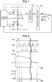
Fig. 1 is a circuit diagram of a capacitance detecting device; and -
Fig. 2 is a timing chart of each signal in the capacitance detecting device. - Hereinafter, an embodiment of the capacitance detecting device will be described with reference to the accompanying drawings. The capacitance detecting device is, for example, a device that is embedded in a door handle of a vehicle and detects whether a user touches the door handle.
- As illustrated in
Fig. 1 , the capacitance detecting device includes a first power source V1 using a direct current. One terminal of afirst capacitor 11 is connected to the first power source V1. Thefirst capacitor 11 has a constant capacitance. Asecond capacitor 12 is connected in series to thefirst capacitor 11. The capacitance of thesecond capacitor 12 is smaller than the capacitance of thefirst capacitor 11. A second power source V2 is connected to a terminal of thesecond capacitor 12, which is opposite to a side connected to thefirst capacitor 11. In the present embodiment, the second power source V2 is a plate-shaped detection electrode disposed in a free space. Thus, the potential of the second power source V2 is approximately a ground level. Further, when a conductor (for example, a finger of a human) approaches the detection electrode, the capacitance of thesecond capacitor 12 is changed. That is, thesecond capacitor 12 functions as a variable capacitor. - A first switch SW1 is connected between the terminal of the
first capacitor 11 on the first power source V1 side and a terminal of thefirst capacitor 11 on thesecond capacitor 12 side. A second switch SW2 is connected between the terminal of thefirst capacitor 11 on thesecond capacitor 12 side and a terminal of thesecond capacitor 12 on thefirst capacitor 11 side. A third switch SW3 is connected between the terminal of thesecond capacitor 12 on thefirst capacitor 11 side and the terminal of thesecond capacitor 12 on the second power source V2 side. The first switch SW1, the second switch SW2, and the third switch SW3 are, for example, MOS transistors, and ON/OFF states of the first switch SW1, the second switch SW2, and the third switch SW3 are controlled depending on a control signal from acontrol circuit 31. - An input terminal of a
filter circuit 40 is connected to a connection node 14 (hereinafter, simply and briefly referred to as the connection node 14) between thefirst capacitor 11 and the second switch SW2. Thefilter circuit 40, which is a so-called low pass filter, transmits a potential of a frequency that is equal to or less than a predetermined frequency (for example, 20 MHz), and does not transmit a potential of a frequency that is more than the predetermined frequency. Switching frequencies of the second switch SW2 and the third switch SW3 are equal to or less than the predetermined frequency. An input terminal of a sample-and-hold circuit 50 is connected to an output terminal of thefilter circuit 40. - The sample-and-
hold circuit 50 operates according to an ON/OFF control of the second switch SW2. In detail, when the second switch SW2 is controlled to be turned on, the sample-and-hold circuit 50 outputs a post-filter potential VMF, which is an output potential of thefilter circuit 40, as a hold potential VMH without changing the post-filter potential VMF as it is. Further, when the second switch SW2 is controlled to be turned off, the sample-and-hold circuit 50 holds the post-filter potential VMF obtained when the second switch SW2 is controlled to be turned off, and outputs the post-filter potential VMF as the hold potential VMH until the second switch SW2 is controlled to be turned on at a next time. In the present embodiment, the sample-and-hold circuit 50 holds the post-filter potential VMF and outputs the post-filter potential VMF as the hold potential VMH, at a delay timing delayed by a predetermined time from a timing when the second switch SW2 is controlled to be turned off. The predetermined time is set to a time which is sufficiently shorter than a switching period of the second switch SW2 and the third switch SW3, and which ranges, for example, from several nanoseconds to several tens of nanoseconds. - A non-inverting input terminal of a
comparator 32 is connected to an output terminal of the sample-and-hold circuit 50. A third power source V3 is connected to an inverting input terminal of thecomparator 32. The third power source V3 is a constant potential power source, and a reference potential Vth, which is the potential of the third power source V3, is lower than the potential of the first power source V1 and is higher than the potential of the second power source V2. When the hold potential VMH input to the non-inverting input terminal is equal to or more than the reference potential Vth input to an inverting input terminal, thecomparator 32 outputs a low-level output signal Vout. Thus, when the hold potential VMH input to the non-inverting input terminal is less than the reference potential Vth input to the inverting input terminal, thecomparator 32 outputs a high-level output signal Vout. An output terminal of thecomparator 32 is connected to thecontrol circuit 31. - The
control circuit 31 controls turning on/off the first switch SW1, the second switch SW2, and the third switch SW3, to detect a change in the capacitance of thesecond capacitor 12. Further, thecontrol circuit 31 controls the sample-and-hold circuit 50 to perform switching between a state in which the sample-and-hold circuit 50 outputs the input potential as it is and a state in which the sample-and-hold circuit 50 holds and outputs the input potential at a predetermined timing. - The
control circuit 31 detects the change in the capacitance of thesecond capacitor 12, based on the output signal Vout of thecomparator 32. Flow at that time will be described below. - As illustrated in
Fig. 2 , at a timing t1, thecontrol circuit 31 starts a process of detecting the change in the capacitance of thesecond capacitor 12, firstly controls to be turned on only the first switch SW1, and controls to be turned off the second switch SW2 and the third switch SW3. Accordingly, thefirst capacitor 11 is discharged so that the potential VM of theconnection node 14 becomes an initial potential which is the potential of the first power source V1. The initial potential is output to the sample-and-hold circuit 50 as the post-filter potential VMF through thefilter circuit 40. The sample-and-hold circuit 50 outputs the post-filter potential VMF as the hold potential VMH as it is to thecomparator 32 without changing the post-filter potential VMF. Thecomparator 32 compares the hold potential VMH with the reference potential Vth, and outputs the low-level output signal Vout to thecontrol circuit 31, based on a result of the comparison. - Thereafter, at a timing t2, the
control circuit 31 controls to be turned on only the second switch SW2, and controls to be turned off the first switch SW1 and the third switch SW3. Accordingly, the potential VM of theconnection node 14 is lowered, and thesecond capacitor 12 is charged. While the second switch SW2 is controlled to be turned on, thefilter circuit 40 outputs, to the sample-and-hold circuit 50, the post-filter potential VMF obtained by filtering the potential VM of theconnection node 14. The sample-and-hold circuit 50 outputs the post-filter potential VMF as the hold potential VMH as it is to thecomparator 32 without changing the post-filter potential VMF. Thecomparator 32 compares the hold potential VMH with the reference potential Vth, and outputs the low-level output signal Vout to thecontrol circuit 31, based on a result of the comparison. - Thereafter, at a timing t3, the
control circuit 31 controls to be turned on only the third switch SW3, and controls to be turned off the first switch SW1 and the second switch SW2. Accordingly, thesecond capacitor 12 is discharged. While the second switch SW2 is controlled to be turned off, thefilter circuit 40 outputs, to the sample-and-hold circuit 50, the post-filter potential VMF obtained by filtering the potential VM of theconnection node 14. The sample-and-hold circuit 50 holds the post-filter potential VMF obtained when the second switch SW2 is controlled to be turned off, and outputs, to thecomparator 32, the post-filter potential VMF as the hold potential VMH until the second switch SW2 is controlled to be turned on at a next time. Thecomparator 32 compares the hold potential VMH with the reference potential Vth, and outputs the low-level output signal Vout to thecontrol circuit 31, based on a result of the comparison. - Thereafter, the
control circuit 31 alternately repeats the control of switching on only the second switch SW2 and the control of switching off only the third switch SW3. Accordingly, the potential VM of theconnection node 14 gradually decreases. Accordingly, the hold potential VMH output to thecomparator 32 by the sample-and-hold circuit 50 also decreases gradually. The hold potential VMH becomes lower than the reference potential Vth soon. At a timing t4 when the hold potential VMH is lower than the reference potential Vth, the output signal Vout of thecomparator 32 becomes a high level. - Here, the
control circuit 31 acquires the output signal Vout of thecomparator 32 whenever the the second switch SW2 is controlled to be turned off. In detail, thecontrol circuit 31 acquires the output signal Vout at a latter half side timing that is later than a central timing while the second switch SW2 is controlled to be turned off. - The
control circuit 31 calculates how many times the control of switching on/off the second switch SW2 is repeated since the detection of the change in the capacitance of thesecond capacitor 12 starts until the high-level output signal Vout is acquired. Thecontrol circuit 31 compares a result of the calculation with a predetermined reference number of times, and detects that the capacitance of thesecond capacitor 12 changes, when a difference therebetween is equal to or more than a specified number of times. The reference number of times is experimentally obtained as the number of times by which the control of switching on/off the second switch SW2 is repeated until the high-level output signal Vout is acquired in a situation in which the conductor does not approach the detection electrode. - Next, an operation of the
filter circuit 40 and the sample-and-hold circuit 50 when thecontrol circuit 31 detects the change in the capacitance of thesecond capacitor 12 will be described. - Electromagnetic noise is mixed in a circuit of the capacitance detecting device. The electromagnetic noise is, for example, electromagnetic noise picked up by the
second capacitor 12 and the second power source V2 (the detection electrode). In detail, since each terminal of thesecond capacitor 12 and the second power source V2 are conductors, the terminals of thesecond capacitor 12 and the second power source V2 function as antennas, and pick up the electromagnetic noise. Thus, when such electromagnetic noise is picked up, a terminal voltage of thesecond capacitor 12 changes. Therefore, in the case where the second switch SW2 is controlled to be turned on, this electromagnetic noise changes the potential VM of theconnection node 14. - Further, the other electromagnetic noise is, for example, electromagnetic noise occurring when the first power source V1 generates a voltage and electromagnetic noise mixed in a wiring from the first power source V1 to the
first capacitor 11. When the electromagnetic noise is picked up, a terminal voltage of thefirst capacitor 11 varies. Therefore, in the case where the second switch SW2 is controlled to be turned off, this electromagnetic noise changes the potential VM of theconnection node 14. - When the above-described electromagnetic noise is included in the potential VM of the
connection node 14, if thecomparator 32 compares the potential VM itself with the reference potential Vth, the following problem may occur. That is, the potential VM of theconnection node 14 changes due to the electromagnetic noise. Due to the change, it can be erroneously determined that the potential VM of theconnection node 14 reaches the reference potential Vth. Otherwise, it can be erroneously determined that the potential VM does not reach the reference potential Vth. - In this regard, in the above-described configuration, the
filter circuit 40 and the sample-and-hold circuit 50 are provided between theconnection node 14 and thecomparator 32. As described above, in the case where the second switch SW2 is controlled to be turned on, the potential VM of theconnection node 14 includes electromagnetic noise from thesecond capacitor 12 side. Thefilter circuit 40 can filter a change in a potential of a frequency, which corresponds to this electromagnetic noise, and can block at least a part of the electromagnetic noise. Thus, the hold potential VMH output to thecomparator 32 by the sample-and-hold circuit 50 is a potential after this filtering. Thus, a potential of which a change caused by the electromagnetic noise is suppressed is input to thecomparator 32. - Further, the potential VM of the
connection node 14 includes electromagnetic noise from the first power source V1. In the case where the second switch SW2 is controlled to be turned off, the sample-and-hold circuit 50 continuously holds the post-filter potential VMF obtained in the case where the second switch SW2 is controlled to be turned off. In this way, when a constant potential is maintained, influence of the electromagnetic noise is not reflected on the hold potential VMH output to thecomparator 32 by the sample-and-hold circuit 50. That is, a potential not including a change caused by the electromagnetic noise is input to thecomparator 32. - According to the present embodiment, the following effects can be obtained.
- (1) Influence of the electromagnetic noise from the potential VM of the
connection node 14, which is used when thecontrol circuit 31 detects the change in the capacitance of thesecond capacitor 12, can be removed by thefilter circuit 40 and the sample-and-hold circuit 50. As a result, detection accuracy of the change in the capacitance of thesecond capacitor 12 is improved. - (2) A small lag may occur due to switching noise of the second switch SW2 until the potential VM of the
connection node 14 is completely stabilized after the second switch SW2 is controlled to be turned off. In this regard, in the above-described configuration, the sample-and-hold circuit 50 holds the post-filter potential VMF at a delay timing delayed by a predetermined time from a timing when the second switch SW2 is controlled to be turned off. Therefore, the output of the post-filter potential VMF as the hold potential VMH, corresponding to the potential VM of theconnection node 14 in an unstable state, to thecomparator 32 is suppressed. Thus, the comparison of the hold potential VMH in an unstable state with the reference potential Vth by thecomparator 32 is suppressed. As a result, improvement of reliability of a result of the comparison by thecomparator 32 is expected. - (3) Immediately after the potential input to the
comparator 32 is changed, a time during which an input potential is reflected in an internal circuit of thecomparator 32 is required, and the potential becomes unstable. Therefore, immediately after the potential input to thecomparator 32 is changed, reliability of output of the result of the comparison by thecomparator 32 deteriorates. In the above-described configuration, the change in the capacitance of thesecond capacitor 12 is detected based on the output signal Vout of thecomparator 32 during a period during which it is considered that the reliability of the result of the comparison is high, which is referred to as a latter half side of a period during which the second switch SW2 is controlled to be turned off. Therefore, when the change in the capacitance of thesecond capacitor 12 is detected based on the result of the comparison by thecomparator 32, improvement of the detection accuracy is expected. - The above-described embodiment can be modified and realized as follows.
- The
control circuit 31 may acquire the output signal Vout from thecomparator 32 at a former half side timing that is earlier than a central timing while the second switch SW2 is controlled to be turned off. At the former half side timing, at a timing delayed to some extent from the timing when the second switch SW2 is switched off, it is considered that the potential input to thecomparator 32 is relatively stable. Therefore, in such a timing, a possibility that the output of the result of the comparison by thecomparator 32 deteriorates is reduced. Even when the potential input to thecomparator 32 is changed by performance, functions, and the like of thecomparator 32, when the potential is stable immediately after the change in the potential, thecontrol circuit 31 may acquire the output signal Vout in any period regardless of whether the second switch SW2 is switched on/off. - The
comparator 32 may be disused, and the hold potential VMH output from the sample-and-hold circuit 50 may be input to thecontrol circuit 31. Thus, the reference potential Vth is stored in thecontrol circuit 31 in advance, and thecontrol circuit 31 may compare the hold potential VMH with the reference potential Vth. - The potential held in the sample-and-
hold circuit 50 during the period during which the second switch SW2 is controlled to be turned off may be set as the post-filter potential VMF at a time point (a timing before the delay timing) at which the second switch SW2 is controlled to be turned off. For example, when a degree to which the potential VM of theconnection node 14 becomes unstable after the second switch SW2 is controlled to be turned off is very small, even when the post-filter potential VMF at a time point when the second switch SW2 is controlled to be turned off is held by the sample-and-hold circuit 50, the reliability of the result of the comparison by thecomparator 32 hardly deteriorates. - The
filter circuit 40 may be connected between the terminal of thesecond capacitor 12 on thefirst capacitor 11 side and the second switch SW2 or between the second switch SW2 and theconnection node 14. In this case, the sample-and-hold circuit 50 needs to be connected between theconnection node 14 and thecomparator 32. - The
filter circuit 40 may not be a low pass filter. For example, thefilter circuit 40 may be a band pass filter that does not allow a potential of a frequency in a specific range to pass therethrough. However, thefilter circuit 40 needs to transmit a potential of a frequency including switching frequencies of the second switch SW2 and the third switch SW3. - A method of detecting the change in the capacitance of the
second capacitor 12 may be based on the potential VM of theconnection node 14. For example, in the above-described embodiment, a period from a time when the detection of the change in the capacitance of thesecond capacitor 12 starts to a time when the high-level output signal Vout is acquired is set as one cycle, and the cycle is repeated. Thus, a time series of the number of times, by which the control of switching on/off the second switch SW2 is repeated and which is calculated at each cycle, is created. When a time change of this time series exceeds an allowable range of a detection error, the change in the capacitance of thesecond capacitor 12 may be detected. - The second power source V2 may be grounded.
- An installation place of the capacitance detecting device is not limited to a door handle of a vehicle. The capacitance detecting device may, for example, be installed inside a door of the vehicle or an emblem of the vehicle. The capacitance detecting device may be installed in a place other than the vehicle.
- The principles, preferred embodiment and mode of operation of the present invention have been described in the foregoing specification. However, the invention which is intended to be protected is not to be construed as limited to the particular embodiments disclosed. Further, the embodiments described herein are to be regarded as illustrative rather than restrictive. Variations and changes may be made by others, and equivalents employed, without departing from the spirit of the present invention. Accordingly, it is expressly intended that all such variations, changes and equivalents which fall within the scope of the present invention as defined in the claims, be embraced thereby.
Claims (3)
- A capacitance detecting device comprising:a first capacitor (11) and a second capacitor (12) that are connected in series to each other between a power source (V1) and a detection electrode (V2);a first switch (SW1) that is connected between terminals of the first capacitor;a second switch (SW2) that is connected between the first capacitor and the second capacitor;a third switch (SW3) that is connected between terminals of the second capacitor;a control circuit (31) that controls turning on/off the first switch, the second switch, and the third switch, is connected to a connection node between the first capacitor and the second switch, and detects a change in a capacitance of the second capacitor based on a potential of the connection node;a filter circuit (40) that is connected to the connection node, transmits a potential of a frequency including switching frequencies of the second switch and the third switch, and does not transmit a potential of another specific frequency; anda sample-and-hold circuit (50) that is connected between the filter circuit and the control circuit,wherein the sample-and-hold circuit outputs a potential according to output of the filter circuit in a case where the second switch is controlled to be turned on, and holds and outputs a potential according to the output of the filter circuit obtained when the second switch is controlled to be turned off, until the second switch is controlled to be turned on at a next time, in a case where the second switch is controlled to be turned off.
- The capacitance detecting device according to claim 1,
wherein in the case where the second switch is controlled to be turned off, the sample-and-hold circuit holds and outputs the potential according to the output of the filter circuit as a potential obtained when the second switch is controlled to be turned off at a delay timing delayed by a predetermined time from a timing when the second switch is controlled to be turned off. - The capacitance detecting device according to claim 1 or 2,
wherein a comparator (32) that compares a potential output by the sample-and-hold circuit with a predetermined reference potential and outputs an output signal to the control circuit based on a result of the comparison is provided between the sample-and-hold circuit and the control circuit, and
the control circuit detects a change in a capacitance of the second capacitor based on the output signal of the comparator at a latter half side timing that is later than a central timing while the second switch is controlled to be turned off.
Applications Claiming Priority (1)
| Application Number | Priority Date | Filing Date | Title |
|---|---|---|---|
| JP2017228082A JP7006189B2 (en) | 2017-11-28 | 2017-11-28 | Capacitance detector |
Publications (3)
| Publication Number | Publication Date |
|---|---|
| EP3490148A2 true EP3490148A2 (en) | 2019-05-29 |
| EP3490148A3 EP3490148A3 (en) | 2019-07-24 |
| EP3490148B1 EP3490148B1 (en) | 2022-11-09 |
Family
ID=64556789
Family Applications (1)
| Application Number | Title | Priority Date | Filing Date |
|---|---|---|---|
| EP18208922.7A Active EP3490148B1 (en) | 2017-11-28 | 2018-11-28 | Capacitance detecting device |
Country Status (4)
| Country | Link |
|---|---|
| US (1) | US10775526B2 (en) |
| EP (1) | EP3490148B1 (en) |
| JP (1) | JP7006189B2 (en) |
| CN (1) | CN109900968B (en) |
Families Citing this family (2)
| Publication number | Priority date | Publication date | Assignee | Title |
|---|---|---|---|---|
| CN110275047B (en) * | 2018-03-14 | 2021-01-22 | 京东方科技集团股份有限公司 | Acceleration sensor, capacitance detection circuit, acceleration processing circuit and method |
| WO2022097327A1 (en) * | 2020-11-09 | 2022-05-12 | 日立Astemo株式会社 | Signal processing device and control method for signal processing device |
Citations (1)
| Publication number | Priority date | Publication date | Assignee | Title |
|---|---|---|---|---|
| JP2005106665A (en) | 2003-09-30 | 2005-04-21 | Aisin Seiki Co Ltd | Capacitance detection device |
Family Cites Families (17)
| Publication number | Priority date | Publication date | Assignee | Title |
|---|---|---|---|---|
| JPS6047678B2 (en) * | 1980-12-08 | 1985-10-23 | 沖電気工業株式会社 | sample hold circuit |
| JPS60171700A (en) * | 1984-02-15 | 1985-09-05 | Toshiba Corp | Sample hold circuit |
| JP2972552B2 (en) * | 1995-05-26 | 1999-11-08 | 日本電気株式会社 | Detection circuit and detection method for capacitive sensor |
| JP3262013B2 (en) * | 1997-02-24 | 2002-03-04 | 三菱電機株式会社 | Capacitive sensor interface circuit |
| JP3264884B2 (en) * | 1998-05-11 | 2002-03-11 | 三菱電機株式会社 | Capacitance detection circuit |
| US6466036B1 (en) | 1998-11-25 | 2002-10-15 | Harald Philipp | Charge transfer capacitance measurement circuit |
| CN100538486C (en) * | 2002-12-25 | 2009-09-09 | 株式会社半导体能源研究所 | Liquid crystal indicator |
| JP4303545B2 (en) | 2003-09-09 | 2009-07-29 | 富士通株式会社 | Movable element device |
| US20080122454A1 (en) * | 2006-11-29 | 2008-05-29 | Aisin Seiki Kabushiki Kaisha | Capacitance detecting apparatus |
| CN101123122A (en) * | 2007-09-14 | 2008-02-13 | 苏州市华芯微电子有限公司 | A data sampling/keeping method and its circuit |
| US8054090B2 (en) * | 2008-10-22 | 2011-11-08 | Atmel Corporation | Noise handling in capacitive touch sensors |
| JP4888743B2 (en) * | 2009-07-09 | 2012-02-29 | アイシン精機株式会社 | Capacitance detection device |
| JP2011194641A (en) | 2010-03-18 | 2011-10-06 | Seiko Epson Corp | Driving circuit for capacitive load |
| JP5429207B2 (en) * | 2010-09-08 | 2014-02-26 | 株式会社デンソー | Capacitive physical quantity detector |
| US9552893B2 (en) * | 2012-08-08 | 2017-01-24 | Nxp Usa, Inc. | Sample-and-hold circuit and capacitive sensing device that includes the sample-and-hold circuit |
| WO2015131209A2 (en) | 2014-02-28 | 2015-09-03 | Azoteq (Pty) Ltd | Charge transfer measurement techniques |
| JP6938854B2 (en) * | 2016-05-10 | 2021-09-22 | 富士電機株式会社 | Switching power supply |
-
2017
- 2017-11-28 JP JP2017228082A patent/JP7006189B2/en active Active
-
2018
- 2018-11-23 CN CN201811405758.8A patent/CN109900968B/en active Active
- 2018-11-28 US US16/202,603 patent/US10775526B2/en active Active
- 2018-11-28 EP EP18208922.7A patent/EP3490148B1/en active Active
Patent Citations (1)
| Publication number | Priority date | Publication date | Assignee | Title |
|---|---|---|---|---|
| JP2005106665A (en) | 2003-09-30 | 2005-04-21 | Aisin Seiki Co Ltd | Capacitance detection device |
Also Published As
| Publication number | Publication date |
|---|---|
| EP3490148A3 (en) | 2019-07-24 |
| JP7006189B2 (en) | 2022-01-24 |
| US20190162869A1 (en) | 2019-05-30 |
| CN109900968B (en) | 2022-08-30 |
| EP3490148B1 (en) | 2022-11-09 |
| CN109900968A (en) | 2019-06-18 |
| JP2019100711A (en) | 2019-06-24 |
| US10775526B2 (en) | 2020-09-15 |
Similar Documents
| Publication | Publication Date | Title |
|---|---|---|
| US9524056B2 (en) | Capacitive voltage information sensing circuit and related anti-noise touch circuit | |
| US8982093B2 (en) | Capacitive touch sensing system with interference rejection | |
| US7119554B2 (en) | Electrical capacitance proximity sensor | |
| US10158360B2 (en) | Capacitive switch having high accuracy | |
| US10168187B2 (en) | Evaluation circuit for a capacitive sensor, capacitive sensor, and actuator in a motor vehicle | |
| KR20190038187A (en) | Apparatus and method for detecting touch | |
| US10775526B2 (en) | Capacitance detecting device | |
| CN108139840A (en) | The device of capacitance detecting | |
| CN112290929B (en) | Signal transmission circuit and electronic equipment | |
| US20160118981A1 (en) | Door handle module for vehicle and apparatus for locking and unlocking vehicle door including the module | |
| JP2011257882A (en) | Touch sensor and touch detection method | |
| US20190260338A1 (en) | Power supply control device | |
| JP2019052943A (en) | Electronic controller | |
| US10021491B2 (en) | Frequency modulated microphone system | |
| JP2022066900A (en) | Proximity detection circuit, proximity detection method, and electronic apparatus | |
| CN100583631C (en) | Transient Detection at the Input of Integrated Circuit Devices | |
| US10684142B2 (en) | Evaluation circuit for a capacitive sensor, capacitive sensor, and actuator in a motor vehicle | |
| CN115149499A (en) | Electronic protection device, control method thereof, chip and electronic equipment | |
| US20140301502A1 (en) | Pulse Signal Outputting Apparatus | |
| US20050093527A1 (en) | [pulse width modulation power regulator and power supply system thereof] | |
| US8466824B2 (en) | Current providing system, ADC with the current providing system, and current providing method | |
| CN119001863A (en) | Interface water inlet detection method and USB Type-C interface chip | |
| CN121325264A (en) | electronic devices | |
| CN210693879U (en) | Signal filtering circuit | |
| US10809827B2 (en) | Pointing stick module and controller |
Legal Events
| Date | Code | Title | Description |
|---|---|---|---|
| PUAI | Public reference made under article 153(3) epc to a published international application that has entered the european phase |
Free format text: ORIGINAL CODE: 0009012 |
|
| STAA | Information on the status of an ep patent application or granted ep patent |
Free format text: STATUS: THE APPLICATION HAS BEEN PUBLISHED |
|
| AK | Designated contracting states |
Kind code of ref document: A2 Designated state(s): AL AT BE BG CH CY CZ DE DK EE ES FI FR GB GR HR HU IE IS IT LI LT LU LV MC MK MT NL NO PL PT RO RS SE SI SK SM TR |
|
| AX | Request for extension of the european patent |
Extension state: BA ME |
|
| PUAL | Search report despatched |
Free format text: ORIGINAL CODE: 0009013 |
|
| AK | Designated contracting states |
Kind code of ref document: A3 Designated state(s): AL AT BE BG CH CY CZ DE DK EE ES FI FR GB GR HR HU IE IS IT LI LT LU LV MC MK MT NL NO PL PT RO RS SE SI SK SM TR |
|
| AX | Request for extension of the european patent |
Extension state: BA ME |
|
| RIC1 | Information provided on ipc code assigned before grant |
Ipc: H03K 5/1252 20060101ALI20190617BHEP Ipc: G11C 27/02 20060101ALI20190617BHEP Ipc: H03K 17/955 20060101AFI20190617BHEP Ipc: G01V 3/08 20060101ALI20190617BHEP Ipc: G01D 5/24 20060101ALN20190617BHEP Ipc: G01R 27/26 20060101ALN20190617BHEP |
|
| STAA | Information on the status of an ep patent application or granted ep patent |
Free format text: STATUS: REQUEST FOR EXAMINATION WAS MADE |
|
| 17P | Request for examination filed |
Effective date: 20200123 |
|
| RBV | Designated contracting states (corrected) |
Designated state(s): AL AT BE BG CH CY CZ DE DK EE ES FI FR GB GR HR HU IE IS IT LI LT LU LV MC MK MT NL NO PL PT RO RS SE SI SK SM TR |
|
| RAP3 | Party data changed (applicant data changed or rights of an application transferred) |
Owner name: AISIN CORPORATION |
|
| GRAP | Despatch of communication of intention to grant a patent |
Free format text: ORIGINAL CODE: EPIDOSNIGR1 |
|
| STAA | Information on the status of an ep patent application or granted ep patent |
Free format text: STATUS: GRANT OF PATENT IS INTENDED |
|
| INTG | Intention to grant announced |
Effective date: 20220610 |
|
| RIC1 | Information provided on ipc code assigned before grant |
Ipc: G01D 5/24 20060101ALN20220527BHEP Ipc: G01R 27/26 20060101ALN20220527BHEP Ipc: G11C 27/02 20060101ALI20220527BHEP Ipc: G01V 3/08 20060101ALI20220527BHEP Ipc: H03K 5/1252 20060101ALI20220527BHEP Ipc: H03K 17/955 20060101AFI20220527BHEP |
|
| GRAS | Grant fee paid |
Free format text: ORIGINAL CODE: EPIDOSNIGR3 |
|
| GRAA | (expected) grant |
Free format text: ORIGINAL CODE: 0009210 |
|
| STAA | Information on the status of an ep patent application or granted ep patent |
Free format text: STATUS: THE PATENT HAS BEEN GRANTED |
|
| AK | Designated contracting states |
Kind code of ref document: B1 Designated state(s): AL AT BE BG CH CY CZ DE DK EE ES FI FR GB GR HR HU IE IS IT LI LT LU LV MC MK MT NL NO PL PT RO RS SE SI SK SM TR |
|
| REG | Reference to a national code |
Ref country code: GB Ref legal event code: FG4D |
|
| REG | Reference to a national code |
Ref country code: CH Ref legal event code: EP Ref country code: AT Ref legal event code: REF Ref document number: 1531028 Country of ref document: AT Kind code of ref document: T Effective date: 20221115 |
|
| REG | Reference to a national code |
Ref country code: DE Ref legal event code: R096 Ref document number: 602018042792 Country of ref document: DE |
|
| REG | Reference to a national code |
Ref country code: IE Ref legal event code: FG4D |
|
| REG | Reference to a national code |
Ref country code: LT Ref legal event code: MG9D |
|
| REG | Reference to a national code |
Ref country code: NL Ref legal event code: MP Effective date: 20221109 |
|
| REG | Reference to a national code |
Ref country code: AT Ref legal event code: MK05 Ref document number: 1531028 Country of ref document: AT Kind code of ref document: T Effective date: 20221109 |
|
| PG25 | Lapsed in a contracting state [announced via postgrant information from national office to epo] |
Ref country code: SE Free format text: LAPSE BECAUSE OF FAILURE TO SUBMIT A TRANSLATION OF THE DESCRIPTION OR TO PAY THE FEE WITHIN THE PRESCRIBED TIME-LIMIT Effective date: 20221109 Ref country code: PT Free format text: LAPSE BECAUSE OF FAILURE TO SUBMIT A TRANSLATION OF THE DESCRIPTION OR TO PAY THE FEE WITHIN THE PRESCRIBED TIME-LIMIT Effective date: 20230309 Ref country code: NO Free format text: LAPSE BECAUSE OF FAILURE TO SUBMIT A TRANSLATION OF THE DESCRIPTION OR TO PAY THE FEE WITHIN THE PRESCRIBED TIME-LIMIT Effective date: 20230209 Ref country code: LT Free format text: LAPSE BECAUSE OF FAILURE TO SUBMIT A TRANSLATION OF THE DESCRIPTION OR TO PAY THE FEE WITHIN THE PRESCRIBED TIME-LIMIT Effective date: 20221109 Ref country code: FI Free format text: LAPSE BECAUSE OF FAILURE TO SUBMIT A TRANSLATION OF THE DESCRIPTION OR TO PAY THE FEE WITHIN THE PRESCRIBED TIME-LIMIT Effective date: 20221109 Ref country code: ES Free format text: LAPSE BECAUSE OF FAILURE TO SUBMIT A TRANSLATION OF THE DESCRIPTION OR TO PAY THE FEE WITHIN THE PRESCRIBED TIME-LIMIT Effective date: 20221109 Ref country code: AT Free format text: LAPSE BECAUSE OF FAILURE TO SUBMIT A TRANSLATION OF THE DESCRIPTION OR TO PAY THE FEE WITHIN THE PRESCRIBED TIME-LIMIT Effective date: 20221109 |
|
| PG25 | Lapsed in a contracting state [announced via postgrant information from national office to epo] |
Ref country code: RS Free format text: LAPSE BECAUSE OF FAILURE TO SUBMIT A TRANSLATION OF THE DESCRIPTION OR TO PAY THE FEE WITHIN THE PRESCRIBED TIME-LIMIT Effective date: 20221109 Ref country code: PL Free format text: LAPSE BECAUSE OF FAILURE TO SUBMIT A TRANSLATION OF THE DESCRIPTION OR TO PAY THE FEE WITHIN THE PRESCRIBED TIME-LIMIT Effective date: 20221109 Ref country code: LV Free format text: LAPSE BECAUSE OF FAILURE TO SUBMIT A TRANSLATION OF THE DESCRIPTION OR TO PAY THE FEE WITHIN THE PRESCRIBED TIME-LIMIT Effective date: 20221109 Ref country code: IS Free format text: LAPSE BECAUSE OF FAILURE TO SUBMIT A TRANSLATION OF THE DESCRIPTION OR TO PAY THE FEE WITHIN THE PRESCRIBED TIME-LIMIT Effective date: 20230309 Ref country code: HR Free format text: LAPSE BECAUSE OF FAILURE TO SUBMIT A TRANSLATION OF THE DESCRIPTION OR TO PAY THE FEE WITHIN THE PRESCRIBED TIME-LIMIT Effective date: 20221109 Ref country code: GR Free format text: LAPSE BECAUSE OF FAILURE TO SUBMIT A TRANSLATION OF THE DESCRIPTION OR TO PAY THE FEE WITHIN THE PRESCRIBED TIME-LIMIT Effective date: 20230210 |
|
| PG25 | Lapsed in a contracting state [announced via postgrant information from national office to epo] |
Ref country code: NL Free format text: LAPSE BECAUSE OF FAILURE TO SUBMIT A TRANSLATION OF THE DESCRIPTION OR TO PAY THE FEE WITHIN THE PRESCRIBED TIME-LIMIT Effective date: 20221109 |
|
| REG | Reference to a national code |
Ref country code: CH Ref legal event code: PL |
|
| REG | Reference to a national code |
Ref country code: BE Ref legal event code: MM Effective date: 20221130 |
|
| PG25 | Lapsed in a contracting state [announced via postgrant information from national office to epo] |
Ref country code: SM Free format text: LAPSE BECAUSE OF FAILURE TO SUBMIT A TRANSLATION OF THE DESCRIPTION OR TO PAY THE FEE WITHIN THE PRESCRIBED TIME-LIMIT Effective date: 20221109 Ref country code: RO Free format text: LAPSE BECAUSE OF FAILURE TO SUBMIT A TRANSLATION OF THE DESCRIPTION OR TO PAY THE FEE WITHIN THE PRESCRIBED TIME-LIMIT Effective date: 20221109 Ref country code: LI Free format text: LAPSE BECAUSE OF NON-PAYMENT OF DUE FEES Effective date: 20221130 Ref country code: EE Free format text: LAPSE BECAUSE OF FAILURE TO SUBMIT A TRANSLATION OF THE DESCRIPTION OR TO PAY THE FEE WITHIN THE PRESCRIBED TIME-LIMIT Effective date: 20221109 Ref country code: DK Free format text: LAPSE BECAUSE OF FAILURE TO SUBMIT A TRANSLATION OF THE DESCRIPTION OR TO PAY THE FEE WITHIN THE PRESCRIBED TIME-LIMIT Effective date: 20221109 Ref country code: CZ Free format text: LAPSE BECAUSE OF FAILURE TO SUBMIT A TRANSLATION OF THE DESCRIPTION OR TO PAY THE FEE WITHIN THE PRESCRIBED TIME-LIMIT Effective date: 20221109 Ref country code: CH Free format text: LAPSE BECAUSE OF NON-PAYMENT OF DUE FEES Effective date: 20221130 |
|
| REG | Reference to a national code |
Ref country code: DE Ref legal event code: R097 Ref document number: 602018042792 Country of ref document: DE |
|
| PG25 | Lapsed in a contracting state [announced via postgrant information from national office to epo] |
Ref country code: SK Free format text: LAPSE BECAUSE OF FAILURE TO SUBMIT A TRANSLATION OF THE DESCRIPTION OR TO PAY THE FEE WITHIN THE PRESCRIBED TIME-LIMIT Effective date: 20221109 Ref country code: LU Free format text: LAPSE BECAUSE OF NON-PAYMENT OF DUE FEES Effective date: 20221128 Ref country code: AL Free format text: LAPSE BECAUSE OF FAILURE TO SUBMIT A TRANSLATION OF THE DESCRIPTION OR TO PAY THE FEE WITHIN THE PRESCRIBED TIME-LIMIT Effective date: 20221109 |
|
| PLBE | No opposition filed within time limit |
Free format text: ORIGINAL CODE: 0009261 |
|
| STAA | Information on the status of an ep patent application or granted ep patent |
Free format text: STATUS: NO OPPOSITION FILED WITHIN TIME LIMIT |
|
| 26N | No opposition filed |
Effective date: 20230810 |
|
| GBPC | Gb: european patent ceased through non-payment of renewal fee |
Effective date: 20230209 |
|
| PG25 | Lapsed in a contracting state [announced via postgrant information from national office to epo] |
Ref country code: IE Free format text: LAPSE BECAUSE OF NON-PAYMENT OF DUE FEES Effective date: 20221128 |
|
| PG25 | Lapsed in a contracting state [announced via postgrant information from national office to epo] |
Ref country code: SI Free format text: LAPSE BECAUSE OF FAILURE TO SUBMIT A TRANSLATION OF THE DESCRIPTION OR TO PAY THE FEE WITHIN THE PRESCRIBED TIME-LIMIT Effective date: 20221109 Ref country code: FR Free format text: LAPSE BECAUSE OF NON-PAYMENT OF DUE FEES Effective date: 20230109 Ref country code: BE Free format text: LAPSE BECAUSE OF NON-PAYMENT OF DUE FEES Effective date: 20221130 |
|
| PG25 | Lapsed in a contracting state [announced via postgrant information from national office to epo] |
Ref country code: GB Free format text: LAPSE BECAUSE OF NON-PAYMENT OF DUE FEES Effective date: 20230209 |
|
| PG25 | Lapsed in a contracting state [announced via postgrant information from national office to epo] |
Ref country code: GB Free format text: LAPSE BECAUSE OF NON-PAYMENT OF DUE FEES Effective date: 20230209 |
|
| PG25 | Lapsed in a contracting state [announced via postgrant information from national office to epo] |
Ref country code: HU Free format text: LAPSE BECAUSE OF FAILURE TO SUBMIT A TRANSLATION OF THE DESCRIPTION OR TO PAY THE FEE WITHIN THE PRESCRIBED TIME-LIMIT; INVALID AB INITIO Effective date: 20181128 |
|
| PG25 | Lapsed in a contracting state [announced via postgrant information from national office to epo] |
Ref country code: CY Free format text: LAPSE BECAUSE OF FAILURE TO SUBMIT A TRANSLATION OF THE DESCRIPTION OR TO PAY THE FEE WITHIN THE PRESCRIBED TIME-LIMIT Effective date: 20221109 |
|
| PG25 | Lapsed in a contracting state [announced via postgrant information from national office to epo] |
Ref country code: MK Free format text: LAPSE BECAUSE OF FAILURE TO SUBMIT A TRANSLATION OF THE DESCRIPTION OR TO PAY THE FEE WITHIN THE PRESCRIBED TIME-LIMIT Effective date: 20221109 Ref country code: IT Free format text: LAPSE BECAUSE OF FAILURE TO SUBMIT A TRANSLATION OF THE DESCRIPTION OR TO PAY THE FEE WITHIN THE PRESCRIBED TIME-LIMIT Effective date: 20221109 |
|
| PG25 | Lapsed in a contracting state [announced via postgrant information from national office to epo] |
Ref country code: MC Free format text: LAPSE BECAUSE OF FAILURE TO SUBMIT A TRANSLATION OF THE DESCRIPTION OR TO PAY THE FEE WITHIN THE PRESCRIBED TIME-LIMIT Effective date: 20221109 |
|
| PG25 | Lapsed in a contracting state [announced via postgrant information from national office to epo] |
Ref country code: TR Free format text: LAPSE BECAUSE OF FAILURE TO SUBMIT A TRANSLATION OF THE DESCRIPTION OR TO PAY THE FEE WITHIN THE PRESCRIBED TIME-LIMIT Effective date: 20221109 Ref country code: MC Free format text: LAPSE BECAUSE OF FAILURE TO SUBMIT A TRANSLATION OF THE DESCRIPTION OR TO PAY THE FEE WITHIN THE PRESCRIBED TIME-LIMIT Effective date: 20221109 |
|
| PG25 | Lapsed in a contracting state [announced via postgrant information from national office to epo] |
Ref country code: BG Free format text: LAPSE BECAUSE OF FAILURE TO SUBMIT A TRANSLATION OF THE DESCRIPTION OR TO PAY THE FEE WITHIN THE PRESCRIBED TIME-LIMIT Effective date: 20221109 |
|
| PG25 | Lapsed in a contracting state [announced via postgrant information from national office to epo] |
Ref country code: MT Free format text: LAPSE BECAUSE OF FAILURE TO SUBMIT A TRANSLATION OF THE DESCRIPTION OR TO PAY THE FEE WITHIN THE PRESCRIBED TIME-LIMIT Effective date: 20221109 |
|
| PGFP | Annual fee paid to national office [announced via postgrant information from national office to epo] |
Ref country code: DE Payment date: 20250930 Year of fee payment: 8 |