EP3490067A1 - Substrate for rfid tags, rfid tag and rfid system - Google Patents
Substrate for rfid tags, rfid tag and rfid system Download PDFInfo
- Publication number
- EP3490067A1 EP3490067A1 EP17831140.3A EP17831140A EP3490067A1 EP 3490067 A1 EP3490067 A1 EP 3490067A1 EP 17831140 A EP17831140 A EP 17831140A EP 3490067 A1 EP3490067 A1 EP 3490067A1
- Authority
- EP
- European Patent Office
- Prior art keywords
- conductor
- rfid tag
- electrode
- capacitance
- electrically connected
- Prior art date
- Legal status (The legal status is an assumption and is not a legal conclusion. Google has not performed a legal analysis and makes no representation as to the accuracy of the status listed.)
- Granted
Links
Images








Classifications
-
- G—PHYSICS
- G06—COMPUTING OR CALCULATING; COUNTING
- G06K—GRAPHICAL DATA READING; PRESENTATION OF DATA; RECORD CARRIERS; HANDLING RECORD CARRIERS
- G06K7/00—Methods or arrangements for sensing record carriers, e.g. for reading patterns
- G06K7/10—Methods or arrangements for sensing record carriers, e.g. for reading patterns by electromagnetic radiation, e.g. optical sensing; by corpuscular radiation
- G06K7/10009—Methods or arrangements for sensing record carriers, e.g. for reading patterns by electromagnetic radiation, e.g. optical sensing; by corpuscular radiation sensing by radiation using wavelengths larger than 0.1 mm, e.g. radio-waves or microwaves
- G06K7/10366—Methods or arrangements for sensing record carriers, e.g. for reading patterns by electromagnetic radiation, e.g. optical sensing; by corpuscular radiation sensing by radiation using wavelengths larger than 0.1 mm, e.g. radio-waves or microwaves the interrogation device being adapted for miscellaneous applications
-
- G—PHYSICS
- G06—COMPUTING OR CALCULATING; COUNTING
- G06K—GRAPHICAL DATA READING; PRESENTATION OF DATA; RECORD CARRIERS; HANDLING RECORD CARRIERS
- G06K19/00—Record carriers for use with machines and with at least a part designed to carry digital markings
- G06K19/06—Record carriers for use with machines and with at least a part designed to carry digital markings characterised by the kind of the digital marking, e.g. shape, nature, code
- G06K19/067—Record carriers with conductive marks, printed circuits or semiconductor circuit elements, e.g. credit or identity cards also with resonating or responding marks without active components
- G06K19/07—Record carriers with conductive marks, printed circuits or semiconductor circuit elements, e.g. credit or identity cards also with resonating or responding marks without active components with integrated circuit chips
- G06K19/077—Constructional details, e.g. mounting of circuits in the carrier
-
- G—PHYSICS
- G06—COMPUTING OR CALCULATING; COUNTING
- G06K—GRAPHICAL DATA READING; PRESENTATION OF DATA; RECORD CARRIERS; HANDLING RECORD CARRIERS
- G06K19/00—Record carriers for use with machines and with at least a part designed to carry digital markings
- G06K19/06—Record carriers for use with machines and with at least a part designed to carry digital markings characterised by the kind of the digital marking, e.g. shape, nature, code
- G06K19/067—Record carriers with conductive marks, printed circuits or semiconductor circuit elements, e.g. credit or identity cards also with resonating or responding marks without active components
- G06K19/07—Record carriers with conductive marks, printed circuits or semiconductor circuit elements, e.g. credit or identity cards also with resonating or responding marks without active components with integrated circuit chips
- G06K19/077—Constructional details, e.g. mounting of circuits in the carrier
- G06K19/0772—Physical layout of the record carrier
- G06K19/07722—Physical layout of the record carrier the record carrier being multilayered, e.g. laminated sheets
-
- G—PHYSICS
- G06—COMPUTING OR CALCULATING; COUNTING
- G06K—GRAPHICAL DATA READING; PRESENTATION OF DATA; RECORD CARRIERS; HANDLING RECORD CARRIERS
- G06K19/00—Record carriers for use with machines and with at least a part designed to carry digital markings
- G06K19/06—Record carriers for use with machines and with at least a part designed to carry digital markings characterised by the kind of the digital marking, e.g. shape, nature, code
- G06K19/067—Record carriers with conductive marks, printed circuits or semiconductor circuit elements, e.g. credit or identity cards also with resonating or responding marks without active components
- G06K19/07—Record carriers with conductive marks, printed circuits or semiconductor circuit elements, e.g. credit or identity cards also with resonating or responding marks without active components with integrated circuit chips
- G06K19/077—Constructional details, e.g. mounting of circuits in the carrier
- G06K19/07745—Mounting details of integrated circuit chips
-
- G—PHYSICS
- G06—COMPUTING OR CALCULATING; COUNTING
- G06K—GRAPHICAL DATA READING; PRESENTATION OF DATA; RECORD CARRIERS; HANDLING RECORD CARRIERS
- G06K19/00—Record carriers for use with machines and with at least a part designed to carry digital markings
- G06K19/06—Record carriers for use with machines and with at least a part designed to carry digital markings characterised by the kind of the digital marking, e.g. shape, nature, code
- G06K19/067—Record carriers with conductive marks, printed circuits or semiconductor circuit elements, e.g. credit or identity cards also with resonating or responding marks without active components
- G06K19/07—Record carriers with conductive marks, printed circuits or semiconductor circuit elements, e.g. credit or identity cards also with resonating or responding marks without active components with integrated circuit chips
- G06K19/077—Constructional details, e.g. mounting of circuits in the carrier
- G06K19/07749—Constructional details, e.g. mounting of circuits in the carrier the record carrier being capable of non-contact communication, e.g. constructional details of the antenna of a non-contact smart card
-
- G—PHYSICS
- G06—COMPUTING OR CALCULATING; COUNTING
- G06K—GRAPHICAL DATA READING; PRESENTATION OF DATA; RECORD CARRIERS; HANDLING RECORD CARRIERS
- G06K19/00—Record carriers for use with machines and with at least a part designed to carry digital markings
- G06K19/06—Record carriers for use with machines and with at least a part designed to carry digital markings characterised by the kind of the digital marking, e.g. shape, nature, code
- G06K19/067—Record carriers with conductive marks, printed circuits or semiconductor circuit elements, e.g. credit or identity cards also with resonating or responding marks without active components
- G06K19/07—Record carriers with conductive marks, printed circuits or semiconductor circuit elements, e.g. credit or identity cards also with resonating or responding marks without active components with integrated circuit chips
- G06K19/077—Constructional details, e.g. mounting of circuits in the carrier
- G06K19/07749—Constructional details, e.g. mounting of circuits in the carrier the record carrier being capable of non-contact communication, e.g. constructional details of the antenna of a non-contact smart card
- G06K19/0775—Constructional details, e.g. mounting of circuits in the carrier the record carrier being capable of non-contact communication, e.g. constructional details of the antenna of a non-contact smart card arrangements for connecting the integrated circuit to the antenna
- G06K19/07754—Constructional details, e.g. mounting of circuits in the carrier the record carrier being capable of non-contact communication, e.g. constructional details of the antenna of a non-contact smart card arrangements for connecting the integrated circuit to the antenna the connection being galvanic
-
- G—PHYSICS
- G06—COMPUTING OR CALCULATING; COUNTING
- G06K—GRAPHICAL DATA READING; PRESENTATION OF DATA; RECORD CARRIERS; HANDLING RECORD CARRIERS
- G06K19/00—Record carriers for use with machines and with at least a part designed to carry digital markings
- G06K19/06—Record carriers for use with machines and with at least a part designed to carry digital markings characterised by the kind of the digital marking, e.g. shape, nature, code
- G06K19/067—Record carriers with conductive marks, printed circuits or semiconductor circuit elements, e.g. credit or identity cards also with resonating or responding marks without active components
- G06K19/07—Record carriers with conductive marks, printed circuits or semiconductor circuit elements, e.g. credit or identity cards also with resonating or responding marks without active components with integrated circuit chips
- G06K19/077—Constructional details, e.g. mounting of circuits in the carrier
- G06K19/07749—Constructional details, e.g. mounting of circuits in the carrier the record carrier being capable of non-contact communication, e.g. constructional details of the antenna of a non-contact smart card
- G06K19/07771—Constructional details, e.g. mounting of circuits in the carrier the record carrier being capable of non-contact communication, e.g. constructional details of the antenna of a non-contact smart card the record carrier comprising means for minimising adverse effects on the data communication capability of the record carrier, e.g. minimising Eddy currents induced in a proximate metal or otherwise electromagnetically interfering object
-
- G—PHYSICS
- G06—COMPUTING OR CALCULATING; COUNTING
- G06K—GRAPHICAL DATA READING; PRESENTATION OF DATA; RECORD CARRIERS; HANDLING RECORD CARRIERS
- G06K19/00—Record carriers for use with machines and with at least a part designed to carry digital markings
- G06K19/06—Record carriers for use with machines and with at least a part designed to carry digital markings characterised by the kind of the digital marking, e.g. shape, nature, code
- G06K19/067—Record carriers with conductive marks, printed circuits or semiconductor circuit elements, e.g. credit or identity cards also with resonating or responding marks without active components
- G06K19/07—Record carriers with conductive marks, printed circuits or semiconductor circuit elements, e.g. credit or identity cards also with resonating or responding marks without active components with integrated circuit chips
- G06K19/077—Constructional details, e.g. mounting of circuits in the carrier
- G06K19/07749—Constructional details, e.g. mounting of circuits in the carrier the record carrier being capable of non-contact communication, e.g. constructional details of the antenna of a non-contact smart card
- G06K19/07773—Antenna details
- G06K19/07786—Antenna details the antenna being of the HF type, such as a dipole
-
- H—ELECTRICITY
- H01—ELECTRIC ELEMENTS
- H01Q—ANTENNAS, i.e. RADIO AERIALS
- H01Q1/00—Details of, or arrangements associated with, antennas
- H01Q1/12—Supports; Mounting means
- H01Q1/22—Supports; Mounting means by structural association with other equipment or articles
- H01Q1/2208—Supports; Mounting means by structural association with other equipment or articles associated with components used in interrogation type services, i.e. in systems for information exchange between an interrogator/reader and a tag/transponder, e.g. in Radio Frequency Identification [RFID] systems
- H01Q1/2225—Supports; Mounting means by structural association with other equipment or articles associated with components used in interrogation type services, i.e. in systems for information exchange between an interrogator/reader and a tag/transponder, e.g. in Radio Frequency Identification [RFID] systems used in active tags, i.e. provided with its own power source or in passive tags, i.e. deriving power from RF signal
-
- H—ELECTRICITY
- H01—ELECTRIC ELEMENTS
- H01Q—ANTENNAS, i.e. RADIO AERIALS
- H01Q1/00—Details of, or arrangements associated with, antennas
- H01Q1/12—Supports; Mounting means
- H01Q1/22—Supports; Mounting means by structural association with other equipment or articles
- H01Q1/2283—Supports; Mounting means by structural association with other equipment or articles mounted in or on the surface of a semiconductor substrate as a chip-type antenna or integrated with other components into an IC package
-
- H—ELECTRICITY
- H01—ELECTRIC ELEMENTS
- H01Q—ANTENNAS, i.e. RADIO AERIALS
- H01Q9/00—Electrically-short antennas having dimensions not more than twice the operating wavelength and consisting of conductive active radiating elements
- H01Q9/04—Resonant antennas
- H01Q9/0407—Substantially flat resonant element parallel to ground plane, e.g. patch antenna
- H01Q9/0421—Substantially flat resonant element parallel to ground plane, e.g. patch antenna with a shorting wall or a shorting pin at one end of the element
-
- H—ELECTRICITY
- H10—SEMICONDUCTOR DEVICES; ELECTRIC SOLID-STATE DEVICES NOT OTHERWISE PROVIDED FOR
- H10W—GENERIC PACKAGES, INTERCONNECTIONS, CONNECTORS OR OTHER CONSTRUCTIONAL DETAILS OF DEVICES COVERED BY CLASS H10
- H10W44/00—Electrical arrangements for controlling or matching impedance
- H10W44/20—Electrical arrangements for controlling or matching impedance at high-frequency [HF] or radio frequency [RF]
- H10W44/241—Electrical arrangements for controlling or matching impedance at high-frequency [HF] or radio frequency [RF] for passive devices or passive elements
- H10W44/248—Electrical arrangements for controlling or matching impedance at high-frequency [HF] or radio frequency [RF] for passive devices or passive elements for antennas
-
- H—ELECTRICITY
- H10—SEMICONDUCTOR DEVICES; ELECTRIC SOLID-STATE DEVICES NOT OTHERWISE PROVIDED FOR
- H10W—GENERIC PACKAGES, INTERCONNECTIONS, CONNECTORS OR OTHER CONSTRUCTIONAL DETAILS OF DEVICES COVERED BY CLASS H10
- H10W70/00—Package substrates; Interposers; Redistribution layers [RDL]
- H10W70/60—Insulating or insulated package substrates; Interposers; Redistribution layers
- H10W70/62—Insulating or insulated package substrates; Interposers; Redistribution layers characterised by their interconnections
- H10W70/63—Vias, e.g. via plugs
-
- H—ELECTRICITY
- H10—SEMICONDUCTOR DEVICES; ELECTRIC SOLID-STATE DEVICES NOT OTHERWISE PROVIDED FOR
- H10W—GENERIC PACKAGES, INTERCONNECTIONS, CONNECTORS OR OTHER CONSTRUCTIONAL DETAILS OF DEVICES COVERED BY CLASS H10
- H10W70/00—Package substrates; Interposers; Redistribution layers [RDL]
- H10W70/60—Insulating or insulated package substrates; Interposers; Redistribution layers
- H10W70/67—Insulating or insulated package substrates; Interposers; Redistribution layers characterised by their insulating layers or insulating parts
- H10W70/68—Shapes or dispositions thereof
- H10W70/682—Shapes or dispositions thereof comprising holes having chips therein
-
- H—ELECTRICITY
- H10—SEMICONDUCTOR DEVICES; ELECTRIC SOLID-STATE DEVICES NOT OTHERWISE PROVIDED FOR
- H10W—GENERIC PACKAGES, INTERCONNECTIONS, CONNECTORS OR OTHER CONSTRUCTIONAL DETAILS OF DEVICES COVERED BY CLASS H10
- H10W90/00—Package configurations
- H10W90/701—Package configurations characterised by the relative positions of pads or connectors relative to package parts
- H10W90/751—Package configurations characterised by the relative positions of pads or connectors relative to package parts of bond wires
- H10W90/754—Package configurations characterised by the relative positions of pads or connectors relative to package parts of bond wires between a chip and a stacked insulating package substrate, interposer or RDL
Definitions
- the present disclosure relates to a radio frequency identification (RFID) tag board that transmits and receives information via a radio wave, an RFID tag, and an RFID system.
- RFID radio frequency identification
- an RFID tag that includes an antenna conductor for performing transmission and reception of information by using a radio wave in an ultra-high frequency (UHF) band or the like and a semiconductor element such as an integrated circuit (IC) or the like is in wide use now.
- UHF ultra-high frequency
- IC integrated circuit
- a signal that is transmitted and received is, for example, stored or retrieved in the semiconductor element.
- the semiconductor element also functions as a power supply unit for the antenna conductor (for example, refer to PTL 1).
- An RFID tag includes an insulating substrate with an upper surface and a lower surface with a recess, an upper surface conductor on the upper surface of the insulating substrate, a ground conductor on the lower surface of the insulating substrate, the ground conductor being electrically connected to the upper surface conductor by a short-circuit portion through conductor that penetrates the insulating substrate in a thickness direction, a capacitance conductor in the insulating substrate, the capacitance conductor facing a portion of the upper surface conductor, a capacitance portion through conductor that penetrates the insulating substrate in the thickness direction from the capacitance conductor to the ground conductor, and a power supply unit in the recess, and the power supply unit includes a first electrode electrically connected to the ground conductor and a second electrode electrically connected to the upper surface conductor.
- An RFID system includes a reader/writer including an antenna that transmits and receives a radio wave to and from an upper surface conductor of the RFID tag configured as described above.
- an RFID tag in the related art since a semiconductor element is mounted on an outer surface of an RFID tag board, it is difficult to improve the reliability of connection between the semiconductor element and the RFID tag board. With respect to the RFID tag, there is a demand for a high-gain antenna property or a wide-bandwidth antenna property. Reduction in size is one of major demands for the RFID tag. With the RFID tag board in the related art, it is difficult to realize the plurality of demands at the same time.
- an upper surface conductor can function as an inverted-F antenna in accordance with electrical connection between a short-circuit portion through conductor, a second electrode, and an upper surface conductor.
- a semiconductor element is located in a recess of an insulating substrate. The recess is provided on a lower surface that is opposite to an upper surface of the insulating substrate on which the upper surface conductor is provided, and a capacitance conductor that faces the upper surface conductor is provided. Therefore, it is possible to achieve reduction in size while improving the reliability of connection between the semiconductor element and the RFID tag board and good basic antenna properties can be achieved with a relatively large upper surface conductor. Furthermore, a higher gain or a wider bandwidth can be achieved depending on where a first electrode is connected to.
- Fig. 1 is a sectional view illustrating an RFID tag according to a first embodiment.
- a first electrode 6 of an RFID tag board 10 is connected to a capacitance conductor 5 by a first connection conductor 8.
- the first electrode 6 of the RFID tag board 10 is connected to a ground conductor 3 by the first connection conductor 8.
- Fig. 2(a) is a bottom view illustrating an example of an exemplary RFID tag board illustrated in Fig. 1(a)
- Fig. 2(b) is an exploded perspective view (an exploded perspective view as seen from a lower surface side) of Fig. 2(a) .
- FIG. 3(a) is a bottom view illustrating an example of an exemplary RFID tag board illustrated in Fig. 1(b) and Fig. 3(b) is an exploded perspective view (an exploded view as seen from a lower surface side) of Fig. 3(a) .
- each through conductor is represented by a broken line and connection portions at the opposite ends thereof are represented by black points.
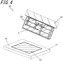
- Fig. 4 is a schematic view illustrating an RFID system according to the embodiment of the disclosure and includes a sectional view of the RFID tag illustrated in Fig. 1(a) and a perspective view of a reader/writer.
- RFID Tag Board and RFID Tag
- the RFID tag 20 includes the RFID tag board 10 and a semiconductor element 11 in the RFID tag board 10.
- the RFID tag board 10 includes, for example, a flat plate-shaped insulating substrate 1 provided with an upper surface and a lower surface with a recess 1a, conductor portions (details will be described later) including an antenna conductor that are provided in the insulating substrate 1, and the like.
- the semiconductor element 11 is mounted in the recess 1a (of the insulating substrate 1) of the RFID tag board 10.
- the semiconductor element 11 is electrically connected to the first electrode 6 and a second electrode 7 of the RFID tag board 10 in the recess 1b.
- the recess 1a may be filled with sealing resin 12 and the semiconductor element 11 may be sealed by being covered by the sealing resin 12.
- the RFID tag board 10 is provided with the recess 1a, the reliability of connection between the semiconductor element 11 and the RFID tag board 10 is improved in comparison with the semiconductor element 11 that is mounted on an outer surface of the RFID tag board 10.
- the semiconductor element 11 in the recess 1a, the first electrode 6, and the second electrode 7 are sealed by the sealing resin 12, contact between these components and the outside air is suppressed, and thus the reliability as the RFID tag 20 is further improved.
- the above-described conductor portions include an upper surface conductor 2 on an upper surface of the insulating substrate 1, the ground conductor 3 on a lower surface of the insulating substrate 1 that is electrically connected to the upper surface conductor 2 by a short-circuit portion through conductor 4 that penetrates the insulating substrate 1 in a thickness direction, the capacitance conductor 5 in the insulating substrate 1 that faces a portion of the upper surface conductor 2, and a capacitance portion through conductor 5a that penetrates the insulating substrate 1 in the thickness direction from the capacitance conductor 5 to the ground conductor 3.
- the above-described conductor portions include the first electrode 6 in the recess 1a that is electrically connected to the capacitance conductor 5 or the ground conductor 3 by the first connection conductor 8 and the second electrode 7 in the recess 1a that is electrically connected to the upper surface conductor 2 via a second connection conductor 9.
- the first electrode 6 is connected to the capacitance conductor 5 by the first connection conductor 8 (a first through conductor 8b).
- the first electrode 6 is connected to the ground conductor 3 by the first connection conductor 8 (a first internal wiring conductor 8a and the first through conductor 8b).
- the second electrode 7 is connected to the upper surface conductor 2 by the second connection conductor 9 (a second through conductor 9b).
- Power supply to the upper surface conductor 2 that functions as the antenna conductor as described later is performed by a power supply unit that includes the above-described first electrode 6, the above-described second electrode 7, and the semiconductor element (a semiconductor integrated circuit element) 11 such as an IC.
- a power supply unit that includes the above-described first electrode 6, the above-described second electrode 7, and the semiconductor element (a semiconductor integrated circuit element) 11 such as an IC.
- the first electrode 6 and the second electrode 7 are provided on a bottom surface of the recess 1a.
- the first electrode 6 and the second electrode 7 are electrically connected to terminals (with no reference numeral) of the semiconductor element 11 via bonding wires 13.
- the first electrode 6 and the second electrode 7 are power supply units for the upper surface conductor 2 and the first electrode 6 and the terminal of the semiconductor element 11 are electrically connected to an end portion of the upper surface conductor 2 via the first connection conductor 8, the short-circuit portion through conductor 4, and the like.
- the second electrode 7 and the terminal of the semiconductor element 11 are electrically connected to a portion of the upper surface conductor 2, which is closer to the central portion than the above-described end portion, via another conductor (the second connection conductor 9) in the insulating substrate 1. Description on details of an antenna function including these power supply units is later given.
- the first through conductor 8b that penetrates the insulating substrate 1 in the thickness direction from the inside of the recess 1a (the first electrode 6) to the capacitance conductor 5 is provided.
- the first electrode 6 and the capacitance conductor 5 are electrically connected to each other by the first through conductor 8b.
- the first through conductor 8b is the first connection conductor 8 and is also included in the above-described conductor portions.
- the first internal wiring conductor 8a is provided from the inside of the recess 1a (the first electrode 6) to the inside of the insulating substrate 1 and the first through conductor 8b that penetrates the insulating substrate 1 in the thickness direction from the first internal wiring conductor 8a to the ground conductor 3 is provided.
- the first electrode 6 and the ground conductor 3 are electrically connected to each other by the first internal wiring conductor 8a and the first through conductor 8b.
- the first internal wiring conductor 8a and the first through conductor 8b constitute the first connection conductor 8 and are also included in the above-described conductor portions.
- the first electrode 6 and the first internal wiring conductor 8a are substantially integrated with each other. Therefore, in the example illustrated in Fig. 1(b) , the first internal wiring conductor 8a may be regarded as an outer end portion of the first electrode 6 extending to the inside of the insulating substrate 1 (between insulating layers 1b which is described later). Alternatively, the first electrode 6 may be regarded as a portion of the first internal wiring conductor 8a.
- the first internal wiring conductor 8a does not need to be formed into one linear conductor having the same width as the first electrode 6 as in an example illustrated in Fig. 3(b) and, for example, the first internal wiring conductor 8a may have a portion with a width larger than that of the first electrode 6 and may have an angled portion as seen in plan view.
- the first internal wiring conductor 8a may be a short conductor that linearly extends up to a connection portion between the first internal wiring conductor 8a and the first through conductor 8b.
- the upper surface conductor 2 can function as an inverted-F antenna in accordance with electrical connection between the short-circuit portion through conductor 4, the second electrode 7, and the upper surface conductor 2.
- the recess 1a of the insulating substrate 1 is provided on a lower surface that is opposite to the upper surface of the insulating substrate 1 on which the upper surface conductor 2 is provided. Therefore, the upper surface conductor 2 can be provided over the entire upper surface of the insulating substrate 1 on which no recess 1a is present and thus the area of the upper surface conductor 2 is increased. Since the upper surface conductor 2, which is a main transmission and reception unit of a radio wave in an antenna, is large, the RFID tag board 10 is a high-gain antenna board that is basically small.
- the capacitance conductor 5 is provided in the insulating substrate 1, it is possible to reduce the size of the RFID tag board 10. Since the capacitance conductor 5 faces the upper surface conductor 2 with no opening formed by the recess 1a, it is possible to increase the size of the capacitance conductor 5, it is possible to increase the capacitance formed between the capacitance conductor 5 and the upper surface conductor 2, and it is possible to reduce the size of the RFID tag board 10.
- the first electrode 7a and the capacitance conductor 5 are electrically connected to each other by the first connection conductor 8 (the first through conductor 8b).
- the first electrode 6 is electrically connected to the ground conductor 3 via the first connection conductor 8 (the first through conductor 8b), the capacitance conductor 5, and the capacitance portion through conductor 5a.
- the first electrode 6 and the ground conductor 3 are electrically connected to each other by the first connection conductor 8.
- the first electrode 6 is directly electrically connected to the ground conductor 3 by the first connection conductor 8 not via the capacitance conductor 5 or the like.
- the RFID tag board 10 in the present embodiment it is possible to provide the small RFID tag 20 which is good in reliability of connection with the semiconductor element 11 and with which it is easy to improve antenna properties of achieving a wide bandwidth or a high gain.
- the insulating substrate 1 functions as an electrically insulating substrate for disposing the conductor portions such as the above-described antenna conductor with the conductor portions being electrically insulated from each other.
- the insulating substrate 1 also functions as a substrate for installing and fixing the semiconductor element 11.
- the insulating substrate 1 has a flat plate-like quadrangular shape such as a square shape or a rectangular shape as in an example illustrated in Figs. 2 and 3 , for example.
- the recess 1a is provided on a predetermined portion such as the central portion of the lower surface of the insulating substrate 1, for example.
- the semiconductor element 11 constituting the power supply unit is located in the recess 1a and the semiconductor element 11 is fixed to the bottom surface of the recess 1a.
- the insulating substrate 1 is formed by using, for example, a ceramic sintered body such as an aluminum oxide sintered body, an aluminum nitride sintered body, a mullite sintered body or a glass ceramic sintered body.
- the insulating substrate 1 is obtained when a plurality of insulating layers 1b is laminated.
- the insulating substrate 1 is configured of a laminate of three insulating layers 1b but the number of the insulating layers 1b is not limited to three. If the insulating substrate 1 is formed by using, for example, an aluminum oxide sintered body, the insulating substrate 1 can be prepared in the following manner.
- base powders of aluminum oxide, silicon oxide or the like are molded into a sheet shape with an appropriate organic binder and an organic solvent and a plurality of quadrangular sheet-shaped ceramic green sheets is prepared.
- the ceramic green sheets are laminated and a laminate is prepared.
- the insulating substrate 1 can be prepared by firing the laminate under a temperature of 1300 to 1600°C.
- the insulating substrate 1 When the firing is performed after a central portion or the like of a portion of the ceramic green sheets is punched in the thickness direction to process the ceramic green sheet into a frame-like shape and the frame-shaped ceramic green sheet is laminated such that the frame-shaped ceramic green sheet becomes the lowermost layer or the like, the insulating substrate 1 provided with the recess 1a can be prepared.
- the insulating substrate 1 is a laminate in which the plurality of insulating layers 1b, each of which is obtained when the ceramic green sheet is sintered, is laminated.
- the conductor portions such as the upper surface conductor 2 or the like are portions constituting the inverted-F antenna in the RFID tag 20 that transmits and receives a radio wave to and from an antenna 32 of a reader/writer 31 which is described later.
- the upper surface conductor 2 is the antenna conductor through which a radio wave is actually transmitted and received and, for example, the upper surface conductor 2 is formed by a conductor layer having a rectangular shape such as a square shape.
- the upper surface conductor 2 is a patch antenna and the power supply unit is electrically connected to an end portion (in an example illustrated in Fig. 2 , an outer peripheral portion that is close to the center of one side of the upper surface conductor 2) of the rectangular antenna conductor via the short-circuit portion through conductor 4.
- the first connection conductor 8, the ground conductor 3, the short-circuit portion through conductor 4, the upper surface conductor 2, and the second connection conductor 9 constitute an electrical connection path between the first electrode 6 and the second electrode 7.
- the capacitance conductor 5 and the capacitance portion through conductor 6 also constitute a portion of the path. Note that, in the example of Fig. 1(b) , the capacitance conductor 5 and the capacitance portion through conductor 6 are not included in the electrical connection path between the first electrode 6 and the second electrode 7.
- the ground conductor 3 is a portion that produces a ground potential to the antenna conductor including the upper surface conductor 2 and is electrically connected to the upper surface conductor 2 by the short-circuit portion through conductor 4.
- the short-circuit portion through conductor 4 is a portion having a function of supplying power to the upper surface conductor 2 as described above and is electrically connected to the power supply units including the first electrode 6.
- the capacitance conductor 5 faces the upper surface conductor 2 with a portion of the insulating substrate 1 (the insulating layer 1b) interposed therebetween, is electrically connected to the ground conductor 3 via the capacitance portion through conductor 5a, and has a function of imparting a predetermined static capacitance to the antenna conductor.
- the capacitance conductor 5 extends toward a central portion from an end that is opposite to an end portion to which the short-circuit portion through conductor 4 is connected.
- the capacitance conductor 5 is electrically connected to the ground conductor 3 by the capacitance portion through conductor 5a at the end that is opposite to the end portion to which the short-circuit portion through conductor 4 is connected.
- the upper surface conductor 2 that has a square shape or the like and has a relatively large area
- the capacitance conductor 5 that faces the upper surface conductor 2 are provided and the power supply units are electrically connected to the end portion of the upper surface conductor 2, it is possible to provide the RFID tag 20 with which it is easy to achieve reduction in size and a high gain as described above.
- the facing area between the capacitance conductor 5 and the upper surface conductor 2 being large is advantageous in the viewpoint of achieving reduction in size.
- the facing area between the capacitance conductor 5 and the upper surface conductor 2 being small is favorable.
- the capacitance conductor 5 and the upper surface conductor 2 may be set to face each other over a range of approximately 10 to 90% of the area of the upper surface conductor 2 as seen in plan view.
- Each of the first electrode 6 and the second electrode 7 included in the power supply units also functions as a connection pad for electrically connecting the terminal of the semiconductor element 11.
- the first electrode 6 and the second electrode 7 are formed into patterns having a quadrangular shape such as a rectangular shape and facilitate connecting the bonding wires 13 through various bonding methods.
- the first connection conductor 8 electrically connects the first electrode 6 and the capacitance conductor 5 or the ground conductor 3.
- the first connection conductor 8 is constituted of the first through conductor 8b penetrating the insulating layer 1b between the first electrode 6 and the capacitance conductor 5 and the first connection conductor 8 connects the first electrode 6 and the capacitance conductor 5.
- the first connection conductor 8 is constituted of the first through conductor 8b penetrating the insulating layer 1b between the first electrode 6 and the capacitance conductor 5 and the first connection conductor 8 connects the first electrode 6 and the capacitance conductor 5.
- the first connection conductor 8 is constituted of the first internal wiring conductor 8a extending from the first electrode 6 to the inside of the insulating substrate 1 (between the insulating layers 1b) and the first through conductor 8b penetrating the insulating layer 1b between the first internal wiring conductor 8a and the ground conductor 3.
- the first connection conductor 8 connects the first electrode 6 and the ground conductor 3.
- the second connection conductor 9 is constituted of the second through conductor 9b penetrating the insulating layers 1b between the second electrode 7 and the upper surface conductor 2 and the second connection conductor 9 directly connects the second electrode 7 and the upper surface conductor 2.
- the second electrode 7 and the upper surface conductor 2 are electrically connected to each other via the second connection conductor 9 and as is described in detail later, the second electrode 7 and the upper surface conductor 2 may be electrically connected to each other by the second connection conductor 9 constituted of a second internal wiring conductor 9a and the second through conductor 9b or may be electrically connected to each other via the second connection conductor 9 and another conductor.
- the conductor portions such as the upper surface conductor 2, the ground conductor 3, the short-circuit portion through conductor 4, the capacitance conductor 5, the capacitance portion through conductor 5a, the first electrode 6, the second electrode 7, the first connection conductor 8 (the first internal wiring conductor 8a and the first through conductor 8b), and the second connection conductor 9 (the second internal wiring conductor 9a and the second through conductor 9b) are formed of, for example, a metal material such as tungsten, molybdenum, manganese, copper, silver, palladium, gold, platinum, nickel, cobalt, or the like. These conductor portions may be formed of an alloy material including the above-described metal material. Such a metal material or the like is provided inside the insulating substrate 1 and on a surface as a metallized conductor.
- the above-described conductor portions can be formed by a method of printing a metallic paste, which is prepared by mixing tungsten powders, an organic solvent, and an organic binder, on predetermined positions on ceramic green sheets, which become the insulating substrate 1 (the insulating layers 1b), through a method such as a screen printing method and firing the ceramic green sheets at the same time thereafter.
- a portion such as the short-circuit portion through conductor 4 that penetrates the insulating substrate 1 (the insulating layers 1b) in the thickness direction can be formed by providing through holes in the ceramic green sheets in advance and firing the ceramic green sheets after filling the through holes with the same metallic paste as described above.
- the through holes can be provided in the ceramic green sheets by a method such as mechanical drilling or laser processing.
- a conductor portion is a metalized layer and is formed on a surface (including the bottom surface of the recess 1a) of the insulating substrate 1
- an exposed surface of the metalized layer may be coated with a nickel plating layer, a gold plating layer, and the like such that oxidation corrosion is suppressed and bonding properties of the bonding wires 9 are improved.
- the semiconductor element 11 is installed in the recess 1a of the RFID tag board 10 as described above and the first electrode 6 and the second electrode 7 are electrically connected to the terminals (with no reference numeral) of the semiconductor element 11. Since the RFID tag board 10 as described above is used, the RFID tag 20 is small, is good in reliability of connection with the semiconductor element 11, and is good in antenna properties of achieving a wide bandwidth or a high gain.
- the semiconductor element 11 functions as a portion of the power supply units described above and also has an information management function such as storing and retrieving a signal transmitted and received between the RFID tag 20 and an external device.
- the semiconductor element 11 is fixed to the bottom surface of the recess 1a.
- the semiconductor element 11 is fixed to the bottom surface of the recess 1a by, for example, a bonding method in which the semiconductor element 11 is fixed via a low melting point brazing material such as gold-silicon wax, a bonding material such as a glass composite material or a resin adhesive.
- the terminals (with no reference numerals) of the semiconductor element 11 are electrically connected to the first electrode 6 and the second electrode 7 via the bonding wires 13.
- the electrical connection between the terminals of the semiconductor element 11 and the first electrode 6 and the second electrode 7 is not limited to this and may be achieved through flip-chip connection using a solder ball, a bump made of metal such as gold, or the like, for example.
- the sealing resin 12 is a portion that covers the semiconductor element 11 to protect the semiconductor element 11 from moisture in the outside air or the outside air such as oxygen, an external mechanical stress, and the like.
- resin materials used to form the sealing resin 12 include epoxy resin, polyimide resin, silicone resin, and the like.
- Filler particles such as silica particles or glass particles may be added to these resin materials. The filler particles are added to adjust various characteristics of the sealing resin 12 such as a mechanical strength, moisture resistance, or electrical characteristics.
- a material for the sealing resin 12 can be selected from those various resin materials and used according to a condition such as workability (productivity) at the time of producing the RFID tag 20 and economic efficiency.
- the RFID tag 20 as described above is used by being mounted on an article in an RFID system 30 which is described later.
- An article 40 on which the RFID tag 20 is mounted is various articles of which a use history is needed when being used.
- examples of the article 40 include tools such as a jig or an industrial tool which is used in various types of industrial processing such as mechanical processing, metal processing, and resin processing. These tools include consumable tools which are cut, polished, or the like.
- the purpose of the article 40 is not limited to an industrial purpose and examples of the article 40 also include daily necessities for home use, agricultural products, various prepaid cards for transport facilities, and medical instruments.
- the RFID tag 20 When mounting the RFID tag 20 to the article 40, it is effective to ground the ground conductor 3 to a metal portion of the article 40.
- the metal portion of the article serves as a ground conductor of an antenna (the above-described inverted-F antenna or the like) of the RFID tag 20, the gain of the antenna is improved, and the communication range of the RFID tag 20 is expanded.
- the RFID system 30 is configured to include the RFID tag 20 configured as described above.
- the RFID system 30 includes the RFID tag 20 configured as described above and the reader/writer 31 including the antenna 32 that transmits and receives a radio wave to and from the upper surface conductor 2 of the RFID tag 20.
- the reader/writer 31 is formed such that the rectangular antenna 32 is provided on a substrate 33 which is formed of, for example, electrically an insulating material.
- the substrate 33 may be a housing (not shown) that accommodates the antenna 32.
- the sealing resin 12 is omitted for simplicity.
- the sealing resin 12 may also be omitted in the following drawings.
- the RFID tag 20 is used by being mounted on various articles 40 and various pieces of information about the article 40 is written in the semiconductor element 11.
- the information can be rewritten at any time according to information that is transmitted and received between the reader/writer 31 and the RFID tag 20 in the RFID system 30 including the RFID tag 20. In this manner, various pieces of information about the article 40 is updated at any time.
- the RFID tag 20 is used while being substantially inverted unlike the example illustrated in Fig. 1 and being close to the reader/writer 31.
- a radio wave emitted from the antenna 32 of the reader/writer 31 is received by the upper surface conductor 2 of the RFID tag 20 and is transmitted to the semiconductor element 11 via the above-described conductor portions, as an electrical signal.
- the upper conductor 2 of the RFID tag 20 and the antenna 32 of the reader/writer 31 do not necessarily face each other in a state as illustrated in, for example, Fig. 4 and any configuration may be adopted as long as a positional relationship can be achieved in which transmission and reception of a radio wave therebetween can be performed.
- a plurality of articles may overlap each other and one article and the reader/writer 31 may be disposed with another article present therebetween.
- Figs. 5(a) and 5(b) are sectional views illustrating another example of the RFID tag according to the first embodiment.
- the way in which the second electrode 7 and the upper surface conductor 2 are electrically connected to each other in the RFID tag board 10 in an example illustrated in Fig. 5 is different from that of the RFID tag board 10 in the example illustrated in Fig. 1 .
- the RFID tag board 10 in the example illustrated in Fig. 5 and the RFID tag board 10 in the example illustrated in Fig. 1 are the same as each other in that the second electrode 7 and the upper surface conductor 2 are connected by the second connection conductor 9 but are different from each other in configuration of the second connection conductor 9.
- Fig. 5(a) and Fig. 1(a) are the same as each other and Fig. 5(b) and Fig. 1(b) are the same as each other.
- Portions in Fig. 5 that are the same as those in Fig. 1 are given the same reference numerals.
- the second internal wiring conductor 9a is provided from the second electrode 7 to the inside of the insulating substrate 1 (between the insulating layers 1b).
- the second internal wiring conductor 9a is electrically connected to the upper surface conductor 2 by the second through conductor 9b extending from the second internal wiring conductor 9a to the upper surface of the insulating substrate 1. That is, in the example illustrated in Fig. 5 , the second connection conductor 9 is constituted of the second internal wiring conductor 9a and the second through conductor 9b.
- the second electrode 7 may be regarded as a portion of the second internal wiring conductor 9a.
- the second internal wiring conductor 9a does not need to be formed into one linear conductor having the same width as the second electrode 7 and, for example, the second internal wiring conductor 9a may have a portion with a width larger than that of the second electrode 7 and may have an angled portion as seen in plan view. If the first connection conductor 8 is connected to the ground conductor 3 and the wiring length between the first electrode 6 and the second electrode 7 is shortened as in an example illustrated in Fig. 5(b) , the second internal wiring conductor 9a may have a linear shape that extends up to a connection portion between the second internal wiring conductor 9a and the second through conductor 9b.
- the second internal wiring conductor 9a may have a curved shape, for example, a meander shape.
- the RFID tag board 10 can have a configuration in which the second electrode 7 is directly electrically connected to the upper surface conductor 2 by the second connection conductor 9 as in the examples illustrated in Figs. 1(a) , 2 , and 5(a) .
- Electrical connection from the first electrode 6 to the second electrode 7 is established in the following order: the first electrode 6, the first connection conductor 8, the capacitance conductor 5, the capacitance portion through conductor 5a, the ground conductor 3, the short-circuit portion through conductor 4, the upper surface conductor 2, and the second connection conductor 9. Therefore, the path is long. Therefore, a transmission loss in the path becomes large and the Q-value in a transmission line becomes low. When the Q-value in the transmission line becomes low, a bandwidth for a frequency becomes wide.
- the RFID tag 20 using such a RFID tag board 10 can be the RFID tag 20 with which it is easy to widen the frequency band of a radio wave transmitted and received in the upper surface conductor 2 and which corresponds to a plurality of RFID systems 30 that uses radio waves in different frequency bands. That is, when one RFID tag 20 is attached to the article 40, it is possible to manage information on the article 40 corresponding to the plurality of RFID systems 30 that transmits and receives radio waves in different frequency bands, for example. In other words, it is not necessary to attach a plurality of RFID tags 20, which corresponds to different frequency bands, to the article 40 and the practicality as the RFID system 30 is improved.
- Fig. 6 is a sectional view illustrating a second embodiment of the RFID tag 20 according to the embodiment of the disclosure.
- An example illustrated in Fig. 6 is an example in which the RFID tag board 10, of which the first electrode 6 is electrically connected to the ground conductor 3 by the first connection conductor 8, is used. Portions in Fig. 6 that are the same as those in Fig. 1 are given the same reference numerals.
- the way in which the second electrode 7 and the upper surface conductor 2 are electrically connected to each other in the second embodiment is different from that in the first embodiment.
- the second electrode 7 is directly electrically connected to the upper surface conductor 2 by the second connection conductor 9.
- the second electrode 7 and the upper surface conductor 2 are electrically connected to each other by the second connection conductor 9 and the short-circuit portion through conductor 4.
- the second electrode 7 is connected to the short-circuit portion through conductor 4 by the second connection conductor 9 (the second internal wiring conductor 9a), the short-circuit portion through conductor 4 being electrically connected to the upper surface conductor 2.
- the second connection conductor 9 is the second internal wiring conductor 9a that extends from the second electrode 7 to the short-circuit portion through conductor 4 inside the insulating substrate 1 (between the insulating layers 1b).
- an electrical connection path from the first electrode 6 and the second electrode 7 is established in the following order: the first electrode 6, the first connection conductor 8 (the first internal wiring conductor 8a and the first through conductor 8b), the ground conductor 3, the short-circuit portion through conductor 4 (a lower surface side portion), and the second connection conductor 9 (the second internal wiring conductor 9a). That is, the path is shorter than that in the examples illustrated in Figs. 1(b) and 5(b) . Therefore, a transmission loss in the path becomes further smaller, and thus the gain of the RFID tag board 10 and the RFID tag 20 becomes high.
- the above-described configuration is also advantageous in the viewpoint of increasing the precision of detected information. That is, when one RFID tag 20 is attached to the article 40, it is possible to transmit and receive information on an article with each in a state where the article 40 and the reader/writer 31 are somewhat separated from each other. Therefore, it is possible to manage information on the article 40 at a high precision and a high speed without bringing the article 40 close to the reader/writer 31 one by one.
- Fig. 7 is a sectional view illustrating a third embodiment of the RFID tag 20 according to the embodiment of the disclosure.
- An example illustrated in Fig. 7 is an example in which the RFID tag board 10, of which the first electrode 6 is electrically connected to the ground conductor 3 by the first connection conductor 8, is used. Portions in Fig. 7 that are the same as those in Fig. 1 are given the same reference numerals.
- the way in which the second electrode 7 and the upper surface conductor 2 are electrically connected to each other in the third embodiment is different from that in the first embodiment.
- the second electrode 7 is directly electrically connected to the upper surface conductor 2 by the second connection conductor 9.
- the second electrode 7 and the upper surface conductor 2 are electrically connected to each other by the second connection conductor 9, the ground conductor 3, and the short-circuit portion through conductor 4.
- the second electrode 7 is connected to the ground conductor 3 by the second connection conductor 9 (the second internal wiring conductor 9a and the second through conductor 9b), the ground conductor 3 being electrically connected to the upper surface conductor 2.
- the second connection conductor 9 is constituted of the second internal wiring conductor 9a extending from the second electrode 7 to the inside of the insulating substrate 1 along the ground conductor 3 and the second through conductor 9b extending from the second internal wiring conductor 9a to the ground conductor 3.
- an electrical connection path from the first electrode 6 and the second electrode 7 is established in the following order: the first electrode 6, the first connection conductor 8 (the first internal wiring conductor 8a and the first through conductor 8b), the ground conductor 3, and the second connection conductor 9 (the second through conductor 9b and the second internal wiring conductor 9a). That is, the wiring length of the connection path is shorter than that in the examples illustrated in Figs. 1(b) , 5(b) and 6 . Therefore, a transmission loss in the path is further reduced, and thus the gain of the RFID tag board 10 and the RFID tag 20 becomes high more effectively. It can be said that the RFID tag board 10 and the RFID tag 20 in the example illustrated in Fig. 7 are effective when focusing on effectively achieving a high-gain antenna conductor.
- the RFID tags 20 in the examples illustrated in Figs. 1 , 5 , 6, and 7 have a configuration made focusing on an effect of achieving a high gain more than an effect of achieving a wide bandwidth, in the following order.
- the RFID tag 20 having a configuration suitable for the RFID system 30 may be used.
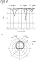
- Figs. 8(a) and (b) respectively illustrate the reflection characteristic and the emission characteristic of each of the RFID tags 20 (the RFID tag boards 10) illustrated in Figs. 5(a), 5(b) , and 7 , the reflection characteristic and the emission characteristic being obtained by an electromagnetic field simulation.
- the horizontal axis of the graph represents a frequency
- the vertical axis represents a reflection characteristic S11
- each of arrows represents a bandwidth with S11 of -5dB or less.
- the vertical axis of the graph represents an antenna gain
- each of values around the graph represents an angle with respect to a zenithal direction as 0° (for example, an upward direction in Fig. 5 ) and each of values pointed by arrows represents an antenna gain at 0°.
- F1 represents the reflection characteristic of the RFID tag 20 illustrated in Fig. 5(a)
- F2 represents the reflection characteristic of the RIFD tag 20 illustrated in Fig. 5(b)
- F3 represents the reflection characteristic of the RIFD tag 20 illustrated in Fig. 7 .
- the bandwidth of F1 is 14.26 MHz
- the bandwidth of F2 is 10.48 MHz
- the bandwidth of F3 is 5.05 MHz.
- a bandwidth F1 of the RFID tag 20 (the RFID tag board 10) in the example illustrated in Fig. 5(a) in which the first electrode 6 is electrically connected to the capacitance conductor 5 is wider than that of the examples illustrated in Figs. 5(b) and 7 in which the first electrode 6 is electrically connected to the ground conductor 3.
- D1 represents the emission characteristic of the RFID tag 20 illustrated in Fig. 5(a)
- D2 represents the emission characteristic of the RIFD tag 20 illustrated in Fig. 5(b)
- D3 represents the emission characteristic of the RIFD tag 20 illustrated in Fig. 7 .
- the antenna gain of D1 is -17.4 dBi
- the antenna gain of D2 is -16.2 dBi
- the antenna gain of D3 is -15.4 dBi.
- the antenna gain D1 of the RFID tag 20 (the RFID tag board 10 in the example illustrated in Fig. 5(a) in which the first electrode 6 is electrically connected to the capacitance conductor 5. Furthermore, the antenna gain D3 in the example illustrated in Fig. 7 in which a connection path from the first electrode 6 to the second electrode 7 is short is higher than the antenna gain D2 in the example illustrated in Fig. 5(b) .
- a bandwidth is wide in the RFID tag 20 in Fig. 5(a) in which the first electrode 6 is electrically connected to the capacitance conductor 5 and a connection path from the first electrode 6 to the second electrode 7 is long.
- the gain of the RFID tags 20 in Figs. 5(b) and 7 in which the first electrode 6 is electrically connected to the ground conductor 3 and a connection path from the first electrode 6 to the second electrode 7 is shorter than that in Fig. 5(a) , is high.
- the gain of the RFID tag 20 in Fig. 7 in which the second electrode 7 is electrically connected to the ground conductor 3 by the second connection conductor 9 is higher than the gain of the RFID tag 20 in Fig. 5(b) in which the second electrode 7 is electrically connected to the short-circuit portion through conductor 4 by the second connection conductor 9.
- Fig. 5(a) and Fig. 5(b) are whether the first connection conductor 8 is connected to the capacitance conductor 5 or to the ground conductor 3.
- the only difference between Fig. 5(b) and Fig. 7 is whether the second through conductor 9b is connected to the short-circuit portion through conductor 4 or to the ground conductor 3.
- Other configurations and materials are the same as each other.
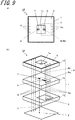
- Fig. 9 illustrates an example of the RFID tag 20 according to a fourth embodiment
- Fig. 9(a) is a bottom view
- Fig. 9(b) is an exploded perspective view of Fig. 9(a) .
- Fig. 9 illustrates only the RFID tag board 10 in the RFID tag 20 with the semiconductor element 11 or the like being omitted for simplicity. Portions in Fig. 9 that are the same as those in Fig. 1 are given the same reference numerals.
- the fourth embodiment is different from the first to third embodiments in the number of short-circuit portion through conductors 4 and the number of capacitance portion through conductors 5a. In an example illustrated in Fig.
- the upper surface conductor 2 and the ground conductor 3 are electrically connected by a plurality of (three) short-circuit portion through conductors 4.
- the capacitance conductor 5 and the ground conductor 3 are electrically connected by a plurality of (three) capacitance portion through conductors 5a.
- the plurality of capacitance portion through conductors 5a and the plurality of short-circuit portion through conductors 4 constitute an electrical connection path from the first electrode 6 to the second electrode 7, it is possible to increase the Q-value of the path and to reduce a loss in comparison with a single capacitance portion through conductor 5a and a single short-circuit portion through conductor 4 being provided. Therefore, it is possible to provide the RFID tag 20 which is effective for more effectively achieving a high gain and for achieving a wide bandwidth.
- the plurality of short-circuit portion through conductors 4 and the plurality of capacitance portion through conductors 5a are provided.
- the configuration in which a plurality of short-circuit portion through conductors 4 and a plurality of capacitance portion through conductors 5a are provided is more effective.
- the number of short-circuit portion through conductors 4 is three and the number of capacitance portion through conductors 5a is three.
- the number is not limited to this.
- the number of short-circuit portion through conductors 4 and the number of capacitance portion through conductors 5a may be different from each other.
- the short-circuit portion through conductors 4 and the capacitance portion through conductors 5a are arranged along sides of the ground conductor 3 that face each other, respectively.
- Figs. 10(a) and (b) respectively illustrate the reflection characteristic and the emission characteristic of each of the RFID tags 20 (the RFID tag boards 10) illustrated in Figs. 5(b) and 9 , the reflection characteristic and the emission characteristic being obtained by an electromagnetic field simulation.
- the horizontal axis of the graph represents a frequency
- the vertical axis represents a reflection characteristic S11
- each of arrows represents a bandwidth with S11 of -5dB or less.
- the vertical axis of the graph represents an antenna gain
- each of values around the graph represents an angle with respect to a zenithal direction as 0° (for example, an upward direction in Fig. 5 ) and each of values pointed by arrows represents an antenna gain at 0°.
- F2 represents the reflection characteristic of the RFID tag 20 illustrated in Fig. 5(b)
- F4 represents the reflection characteristic of the RIFD tag 20 illustrated in Fig. 9 .
- the bandwidth of F2 is 10.48 MHz and the bandwidth of F4 is 7.81 MHz.
- a bandwidth F2 of the RFID tag 20 (the RFID tag board 10) in the example illustrated in Fig. 5(b) in which the number of short-circuit portion through conductors 4 and the number of capacitance portion through conductors 5a are small is wider than a bandwidth F4 of the RFID tag 20 (the RFID tag board 10) in the example illustrated in Fig. 9 in which the number of short-circuit portion through conductors 4 and the number of capacitance portion through conductors 5a are large.
- D2 represents the emission characteristic of the RFID tag 20 illustrated in Fig. 5(b) and D4 represents the emission characteristic of the RIFD tag 20 illustrated in Fig. 9 .
- the antenna gain of D2 is - 16.2 dBi and the antenna gain of D4 is -14.8 dBi.
- D4 of the RFID tag 20 (the RFID tag board 10) in the example illustrated in Fig. 9 in which the number of short-circuit portion through conductors 4 and the number of capacitance portion through conductors 5a are large, is a higher gain.
- a bandwidth is wide in the RFID tag 20 in Fig. 5(b) in which the number of short-circuit portion through conductors 4 and the number of capacitance portion through conductors 5a are small and the gain of the RFID tag 20 in Fig. 9 , in which the number of short-circuit portion through conductors 4 and the number of capacitance portion through conductors 5a are larger than those in Fig. 5(b) , is high.
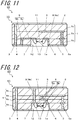
- Fig. 11 is a sectional view illustrating a fifth embodiment of the RFID tag 20.
- the way in which the first electrode 6 and the ground conductor 3 are electrically connected to each other in the fifth embodiment is different from that in the first to fourth embodiments.
- the first connection conductor 8 is constituted of the first internal wiring conductor 8a and the first through conductor 8b.
- the first connection conductor 8 is constituted of a recess side-surface conductor 8c.
- An example illustrated in Fig. 11 is the same as the example illustrated in Fig.
- the first electrode 6 is electrically connected to the ground conductor 3 by the recess side-surface conductor 8c as described above, the volume of a space for the conductor portions in the insulating substrate 1 or the like is reduced. Therefore, the above-described configuration is advantageous in the viewpoint of achieving reduction in size of the RFID tag 20. Since it is possible to shorten a wiring length from the first electrode 6 to the second electrode 7 in comparison with the first connection conductor 8 being constituted of the first internal wiring conductor 8a and the first through conductor 8b, the first electrode 6 being electrically to the ground conductor 3 by the recess-side surface conductor 8c is also advantageous in the viewpoint of achieving a high gain.
- Fig. 12 is a sectional view illustrating a sixth embodiment of the RFID tag 20.
- the way in which the first electrode 6 and the capacitance conductor 5 are electrically connected to each other in the sixth embodiment is different from that in the first embodiment.
- the first connection conductor 8 is constituted of the first through conductor 8b.
- the first connection conductor 8 is constituted of the first internal wiring conductor 8a and two first through conductors 8b.
- An example illustrated in Fig. 12 is the same as the example illustrated in Fig.
- the first connection conductor 8 is connected to an end portion of the capacitance conductor 5 that is opposite to an end portion to which the capacitance portion through conductor 5a is connected. Therefore, in a sectional view as illustrated in Fig. 12 , the first connection conductor 8 constituted of the first internal wiring conductor 8a and the two first through conductors 8b has a curved shape.
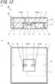
- Fig. 13 illustrates a seventh embodiment of the RFID tag 20 according to the embodiment of the invention.
- Fig. 13(a) is a sectional view and Fig. 13(b) is a bottom view.
- the first electrode 6 is electrically connected to the capacitance conductor 5 by the first connection conductor 8 (the first through conductor 8b) extending from the inside of the recess 1a to the capacitance conductor 5.
- the first connection conductor 8 the first through conductor 8b
- the first electrode 6 and the capacitance conductor 5 are connected to each other by the first connection conductor 8, which is not the first through conductor 8b but the first internal wiring conductor 8a.
- the first electrode 6 and the first internal wiring conductor 8a are substantially integrated with each other. Therefore, it can be said that the first electrode 6 and the capacitance conductor 5 are directly connected to each other. Since the capacitance conductor 5 and the first electrode 6 are disposed between the same insulating layers 1b and the first connection conductor 8 does not include the first through conductor 8b that penetrates the insulating layer 1b, the above-described configuration is advantageous in the viewpoint of achieving reduction in thickness of the RFID tag board 10 and reduction in thickness as the RFID tag 20.
- the width of the capacitance conductor 5 is larger than that in the examples illustrated in Figs. 1(a) and 2(a) .
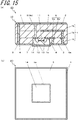
- Figs. 14 to 17 illustrate an eighth embodiment of the RFID tag 20 according to the embodiment of the disclosure.
- the RFID tag 20 includes a conductive lid 14 that covers the recess 1a.
- the examples illustrated in Figs. 14 to 16 are examples in which the RFID tag board 10 in the example illustrated in Fig. 1(a) is used.
- the examples illustrated in Figs. 15 and 17 are examples in which the RFID tag board 10 in the example illustrated in Fig. 1(b) is used.
- the RFID tag 20 is fixed to the article 40 by using, for example, a bonding material such as a resin adhesive or a double sided tape. If the article 40 is conductive, a capacitance component is formed between the upper surface conductor 2 and the article 40.
- a bonding material such as a resin adhesive or a double sided tape.
- the thickness of an adhesive that fixes the RFID tag 20 to the article 40 is changed, the distance between the upper surface conductor 2 and the article 40 is changed, the capacitance component formed therebetween is also changed, and the resonant frequency of the RFID tag 20 is shifted.
- the thickness of the above-described bonding material does not usually become constant due to unevenness in thickness of the bonding material itself such as a double sided tape or due to unevenness in pressing force at the time of bonding.
- the articles 40 may include an article 40 that can communicate with the reader/writer 31 and an article 40 that cannot communicate with the reader/writer 31 even when the articles 40 are provided with the same RFID tags 20.
- the capacitance component is formed between the upper surface conductor 2 and the conductive lid 14 instead of being formed between the upper surface conductor 2 and the article 40. Since the capacitance component is constant regardless of the thickness of the bonding material, unevenness in resonant frequency of the RFID tag 20 is suppressed.
- the conductive lid 14 is fixed to the insulating substrate 1 while covering the recess 1a.
- the conductive lid 14 is disposed to overlap the ground conductor 3, is bonded to the ground conductor 3 by a bonding material (not shown), and is fixed to the insulating substrate 1 via the ground conductor 3.
- the conductive lid 14 and the ground conductor 3 can be electrically connected to each other.
- the conductive lid 14 also functions as a ground conductor and the same effect as when the size of the ground conductor 3 is increased can be achieved.
- the conductive lid 14 and the ground conductor 3 may be mechanically connected to each other by using a bonding material after electrically connecting the conductive lid 14 and the ground conductor 3 to each other by bring the conductive lid 14 and the ground conductor 3 into contact with each other and electrical connection between the conductive lid 14 and the ground conductor 3 and mechanical bonding between the conductive lid 14 and the ground conductor 3 may be performed at the same time by using a conductive bonding material.
- the conductive lid 14 that is larger than the opening of the recess 1a covers the recess 1a, an outer peripheral portion of the conductive lid 14 overlaps with the ground conductor 3, and thus a configuration in which there is no non-conductive portion in plan view can be achieved. If the opening of the ground conductor 3 is larger than the opening of the recess 1a, the conductive lid 14 that is larger than the opening of the ground conductor 3 may be used such that the outer peripheral portion of the conductive lid 14 overlaps with the ground conductor 3. If the conductive lid 14 is smaller than the opening of the ground conductor 3, a conductive substance may be disposed between the conductive lid 14 and the ground conductor 3.
- the outer peripheral portion of the conductive lid 14 and the ground conductor 3 may be connected to each other by using a conductive bonding material such as a conductive adhesive or the like.
- the opening of the ground conductor 3 is not formed to be extremely larger than the opening of the recess 1a usually and thus almost no capacitance component is formed between the upper surface conductor 2 and the article 40 if the conductive lid 14 covers the recess 1a but it is possible to more reliably suppress formation of the capacitance component.
- the conductive lid 14 examples include metal such as copper, stainless steel, and a Fe-Ni-Co alloy, conductive resin in which conductive particles such as metal are dispersed in an insulating material such as resin, and a material made of carbon.
- a substance obtained by providing a conductive film on a surface of an insulating plate may also be used.
- a metal film may be provided on a resin plate, a ceramic plate, or the like through electroless plating or a substance obtained by providing a metalized layer on a ceramic plate or a substance obtained by pasting a metal foil on a resin board may also be used.
- a plate member formed of these materials may be bonded as the conductive lid 14 by using a bonding material.
- the conductive lid 14 is formed of metal, for corrosion protection or improvement in bonding properties of a brazing material or solder, a plating coat of Ni, Au, or the like may be formed on a surface, for example. If the insulating substrate 1 is formed of a ceramic material and the conductive lid 14 is formed of metal, the conductive lid 14 with a high bonding reliability is achieved when a Fe-Ni-Co alloy, of which the thermal expansion coefficient is close to that of a ceramic material, is used as the conductive lid 14. If the recess 1a is air-tightly sealed by the conductive lid 14 and a bonding material, the sealing resin 12 may not be provided.
- the sealing resin 12 If the recess 1a is sealed by the sealing resin 12, it is possible to form and bond the conductive lid 14 by applying liquid conductive resin on the sealing resin 12 and curing the liquid conductive resin and it is also possible to achieve electrical connection with the ground conductor 3 at the same time when the conductive resin is applied from a position above the sealing resin 12 in the recess 1a to a position above the ground conductor 3.
- Examples of a conductive bonding material for fixing the conductive lid 14 to the insulating substrate 1 include metal such as solder and an AuSn wax and a substance obtained by mixing conductive particles such as metal into an insulating material such as resin or glass, and examples of an insulating bonding material for fixing the conductive lid 14 to the insulating substrate 1 include glass or a resin adhesive.
- the size of the conductive lid 14 in plan view may be any size as long as the recess 1a can be covered and may be a size larger than that of the insulating substrate 1 as in the examples illustrated in Figs. 16 and 17 . Even when a portion of the upper surface conductor 2 does not overlap with the ground conductor 3 in plan view due to positional deviation or the like, since the upper surface conductor 2 overlaps with the conductive lid 14 that is larger than the insulating substrate 1, it is possible to suppress the above-described shift in resonant frequency which is caused by a change in capacity component. Since it is possible to increase the adhesion area between the RFID tag 20 and the article 40, it is possible to increase the bonding reliability. As in the examples illustrated in Figs.
- a through hole 14a may be provided in a portion of the conductive lid 14 that protrudes from the insulating substrate 1 and a screw hole may be provided in the article 40 such that the article 40 is fixed by using a screw 15. Even it is possible to firmly fix the RFID tag 20 to the article 40 and it is possible to achieve the RFID tag 20 with a high reliability. It is possible to efficiently release heat, which is generated from the RFID tag 20, toward the article 40 via the screw 15 and the bonding material.
- the conductive lid 14 has a rectangular shape that greatly protrudes with respect to the insulating substrate 1 in a right-left direction in the drawings.
- the shape of the conductive lid 14 is not limited to the rectangular shape and the conductive lid 14 may have a square shape and only a portion corresponding to the screw hole formed in the article 40 may protrude.
- a distance D1 (refer to Fig. 1 ) between the capacitance conductor 5 and the upper surface conductor 2 may be set to be equal to or smaller than one-fourth of a distance D2 (refer to Fig. 1 ) between the ground conductor 3 and the upper surface conductor 2.
- the distances are set as described such that D1/D2 ⁇ 1/4(D2 ⁇ 4 ⁇ D1) is satisfied, it is possible to decrease the distance D1 between the capacitance conductor 5 and the upper surface conductor 2, which contribute to achieving a small-sized antenna, while securing a large distance D2 between the ground conductor 3 and the upper surface conductor 2, which contribute to achieving a high-gain antenna, and thus it is possible to increase the gain of the RFID tag 20 and to decrease the size of the RFID tag 20. It is possible to secure a thickness (D2) of the insulating substrate 1 necessary for providing the recess 1a and thus it is possible to realize the small RFID tag 20.
Landscapes
- Engineering & Computer Science (AREA)
- Microelectronics & Electronic Packaging (AREA)
- Physics & Mathematics (AREA)
- Computer Hardware Design (AREA)
- General Physics & Mathematics (AREA)
- Theoretical Computer Science (AREA)
- Electromagnetism (AREA)
- Toxicology (AREA)
- Health & Medical Sciences (AREA)
- Computer Networks & Wireless Communication (AREA)
- General Health & Medical Sciences (AREA)
- Artificial Intelligence (AREA)
- Computer Vision & Pattern Recognition (AREA)
- Details Of Aerials (AREA)
- Parts Printed On Printed Circuit Boards (AREA)
- Variable-Direction Aerials And Aerial Arrays (AREA)
- Waveguide Aerials (AREA)
Abstract
Description
- The present disclosure relates to a radio frequency identification (RFID) tag board that transmits and receives information via a radio wave, an RFID tag, and an RFID system.
- Detecting and managing information on various articles by using an RFID tag mounted on an article have become widely used techniques. As the RFID tag, an RFID tag that includes an antenna conductor for performing transmission and reception of information by using a radio wave in an ultra-high frequency (UHF) band or the like and a semiconductor element such as an integrated circuit (IC) or the like is in wide use now.
- Information is transmitted and received between the antenna conductor of the RFID tag and an external device such as a reader/writer having a function of transmitting and receiving a radio wave. A signal that is transmitted and received is, for example, stored or retrieved in the semiconductor element. The semiconductor element also functions as a power supply unit for the antenna conductor (for example, refer to PTL 1).
- PTL 1: Japanese Unexamined Patent Application Publication No.
2000-101335 - An RFID tag according to an embodiment of the disclosure includes an insulating substrate with an upper surface and a lower surface with a recess, an upper surface conductor on the upper surface of the insulating substrate, a ground conductor on the lower surface of the insulating substrate, the ground conductor being electrically connected to the upper surface conductor by a short-circuit portion through conductor that penetrates the insulating substrate in a thickness direction, a capacitance conductor in the insulating substrate, the capacitance conductor facing a portion of the upper surface conductor, a capacitance portion through conductor that penetrates the insulating substrate in the thickness direction from the capacitance conductor to the ground conductor, and a power supply unit in the recess, and the power supply unit includes a first electrode electrically connected to the ground conductor and a second electrode electrically connected to the upper surface conductor.
- An RFID system according to an embodiment of the disclosure includes a reader/writer including an antenna that transmits and receives a radio wave to and from an upper surface conductor of the RFID tag configured as described above.
-
-
Figs. 1(a) and 1(b) are sectional views illustrating an example of an RFID tag according to a first embodiment. -
Fig. 2(a) is a bottom view illustrating an example of an RFID tag board in an example illustrated inFig. 1(a) as seen from a lower surface side andFig. 2(b) is an exploded perspective view ofFig. 2(a) . -
Fig. 3(a) is a bottom view illustrating an example of the RFID tag board in an example illustrated inFig. 1(b) as seen from the lower surface side andFig. 3(b) is an exploded perspective view ofFig. 3(a) . -
Fig. 4 is a schematic view illustrating an example of an RFID system according to an embodiment of the disclosure. -
Figs. 5(a) and 5(b) are sectional views illustrating another example of the RFID tag according to the first embodiment. -
Fig. 6 is a sectional view illustrating another example of an RFID tag according to a second embodiment. -
Fig. 7 is a sectional view illustrating another example of an RFID tag according to a third embodiment. -
Fig. 8(a) illustrates bandwidths of the RFID tags illustrated inFigs. 5(a), 5(b) , and7 andFig. 8(b) illustrates antenna gains thereof. -
Fig. 9 illustrates an example of an RFID tag according to a fourth embodiment, whereFig. 9(a) is a bottom view andFig. 9(b) is an exploded perspective view ofFig. 9(a) . -
Fig. 10(a) illustrates bandwidths of the RFID tags illustrated inFigs. 5(b) and9 andFig. 10(b) illustrates antenna gains thereof. -
Fig. 11 is a sectional view illustrating an example of an RFID tag according to a fifth embodiment. -
Fig. 12 is a sectional view illustrating an example of an RFID tag according to a sixth embodiment. -
Fig. 13 illustrates an example of an RFID tag according to a seventh embodiment, whereFig. 13(a) is a sectional view andFig. 13(b) is a bottom view. -
Fig. 14 illustrates an example of an RFID tag according to an eighth embodiment, whereFig. 14(a) is a sectional view andFig. 14(b) is a bottom view. -
Fig. 15 illustrates another example of the RFID tag according to the eighth embodiment, whereFig. 15(a) is a sectional view andFig. 15(b) is a bottom view. -
Fig. 16 illustrates still another example of the RFID tag according to the eighth embodiment, whereFig. 16(a) is a sectional view andFig. 16(b) is a bottom view. -
Fig. 17 illustrates still another example of the RFID tag according to the eighth embodiment, whereFig. 17(a) is a sectional view andFig. 17(b) is a bottom view. Description of Embodiments - In an RFID tag in the related art, since a semiconductor element is mounted on an outer surface of an RFID tag board, it is difficult to improve the reliability of connection between the semiconductor element and the RFID tag board. With respect to the RFID tag, there is a demand for a high-gain antenna property or a wide-bandwidth antenna property. Reduction in size is one of major demands for the RFID tag. With the RFID tag board in the related art, it is difficult to realize the plurality of demands at the same time.
- According to an RFID tag board in an embodiment of the disclosure, since conductor portions having the above-described configuration are provided, an upper surface conductor can function as an inverted-F antenna in accordance with electrical connection between a short-circuit portion through conductor, a second electrode, and an upper surface conductor. In addition, a semiconductor element is located in a recess of an insulating substrate. The recess is provided on a lower surface that is opposite to an upper surface of the insulating substrate on which the upper surface conductor is provided, and a capacitance conductor that faces the upper surface conductor is provided. Therefore, it is possible to achieve reduction in size while improving the reliability of connection between the semiconductor element and the RFID tag board and good basic antenna properties can be achieved with a relatively large upper surface conductor. Furthermore, a higher gain or a wider bandwidth can be achieved depending on where a first electrode is connected to.
- An RFID tag board, an RFID tag, and an RFID system according to embodiments of the disclosure will be described with reference to attached drawings. Note that, upper and lower sides are determined for convenience of explanation in the following description and upper and lower sides at the time of actual use of the RFID tag board, the RFID tag, and the RFID system are not limited thereto.
-
Fig. 1 is a sectional view illustrating an RFID tag according to a first embodiment. In anRFID tag 20 inFig. 1(a) , afirst electrode 6 of anRFID tag board 10 is connected to acapacitance conductor 5 by afirst connection conductor 8. Meanwhile, in theRFID tag 20 inFig. 1(b) , thefirst electrode 6 of theRFID tag board 10 is connected to aground conductor 3 by thefirst connection conductor 8.Fig. 2(a) is a bottom view illustrating an example of an exemplary RFID tag board illustrated inFig. 1(a) andFig. 2(b) is an exploded perspective view (an exploded perspective view as seen from a lower surface side) ofFig. 2(a) .Fig. 3(a) is a bottom view illustrating an example of an exemplary RFID tag board illustrated inFig. 1(b) andFig. 3(b) is an exploded perspective view (an exploded view as seen from a lower surface side) ofFig. 3(a) . InFigs. 2 and3 , each through conductor is represented by a broken line and connection portions at the opposite ends thereof are represented by black points.Fig. 4 is a schematic view illustrating an RFID system according to the embodiment of the disclosure and includes a sectional view of the RFID tag illustrated inFig. 1(a) and a perspective view of a reader/writer. - The
RFID tag 20 according to the embodiment includes theRFID tag board 10 and asemiconductor element 11 in theRFID tag board 10. TheRFID tag board 10 includes, for example, a flat plate-shapedinsulating substrate 1 provided with an upper surface and a lower surface with arecess 1a, conductor portions (details will be described later) including an antenna conductor that are provided in theinsulating substrate 1, and the like. Thesemiconductor element 11 is mounted in therecess 1a (of the insulating substrate 1) of theRFID tag board 10. Thesemiconductor element 11 is electrically connected to thefirst electrode 6 and asecond electrode 7 of theRFID tag board 10 in therecess 1b. As in an example illustrated inFig. 1(b) , therecess 1a may be filled with sealingresin 12 and thesemiconductor element 11 may be sealed by being covered by the sealingresin 12. - As described above, since the
RFID tag board 10 is provided with therecess 1a, the reliability of connection between thesemiconductor element 11 and theRFID tag board 10 is improved in comparison with thesemiconductor element 11 that is mounted on an outer surface of theRFID tag board 10. When thesemiconductor element 11 in therecess 1a, thefirst electrode 6, and thesecond electrode 7 are sealed by the sealingresin 12, contact between these components and the outside air is suppressed, and thus the reliability as theRFID tag 20 is further improved. - The above-described conductor portions include an
upper surface conductor 2 on an upper surface of theinsulating substrate 1, theground conductor 3 on a lower surface of theinsulating substrate 1 that is electrically connected to theupper surface conductor 2 by a short-circuit portion throughconductor 4 that penetrates theinsulating substrate 1 in a thickness direction, thecapacitance conductor 5 in theinsulating substrate 1 that faces a portion of theupper surface conductor 2, and a capacitance portion throughconductor 5a that penetrates theinsulating substrate 1 in the thickness direction from thecapacitance conductor 5 to theground conductor 3. The above-described conductor portions include thefirst electrode 6 in therecess 1a that is electrically connected to thecapacitance conductor 5 or theground conductor 3 by thefirst connection conductor 8 and thesecond electrode 7 in therecess 1a that is electrically connected to theupper surface conductor 2 via asecond connection conductor 9. In an example illustrated inFig. 1(a) , thefirst electrode 6 is connected to thecapacitance conductor 5 by the first connection conductor 8 (a first throughconductor 8b). In the example illustrated inFig. 1(b) , thefirst electrode 6 is connected to theground conductor 3 by the first connection conductor 8 (a firstinternal wiring conductor 8a and the first throughconductor 8b). In the examples illustrated inFigs. 1(a) and 1(b) , thesecond electrode 7 is connected to theupper surface conductor 2 by the second connection conductor 9 (a second throughconductor 9b). - Power supply to the
upper surface conductor 2 that functions as the antenna conductor as described later is performed by a power supply unit that includes the above-describedfirst electrode 6, the above-describedsecond electrode 7, and the semiconductor element (a semiconductor integrated circuit element) 11 such as an IC. - In the
RFID tag 20 according to the embodiment, thefirst electrode 6 and thesecond electrode 7 are provided on a bottom surface of therecess 1a. In an example illustrated inFig. 1 , thefirst electrode 6 and thesecond electrode 7 are electrically connected to terminals (with no reference numeral) of thesemiconductor element 11 viabonding wires 13. Thefirst electrode 6 and thesecond electrode 7 are power supply units for theupper surface conductor 2 and thefirst electrode 6 and the terminal of thesemiconductor element 11 are electrically connected to an end portion of theupper surface conductor 2 via thefirst connection conductor 8, the short-circuit portion throughconductor 4, and the like. Thesecond electrode 7 and the terminal of thesemiconductor element 11 are electrically connected to a portion of theupper surface conductor 2, which is closer to the central portion than the above-described end portion, via another conductor (the second connection conductor 9) in the insulatingsubstrate 1. Description on details of an antenna function including these power supply units is later given. - In the example illustrated in
Fig. 1(a) , the first throughconductor 8b that penetrates the insulatingsubstrate 1 in the thickness direction from the inside of therecess 1a (the first electrode 6) to thecapacitance conductor 5 is provided. Thefirst electrode 6 and thecapacitance conductor 5 are electrically connected to each other by the first throughconductor 8b. In this example, the first throughconductor 8b is thefirst connection conductor 8 and is also included in the above-described conductor portions. - In the example illustrated in
Fig. 1(b) , the firstinternal wiring conductor 8a is provided from the inside of therecess 1a (the first electrode 6) to the inside of the insulatingsubstrate 1 and the first throughconductor 8b that penetrates the insulatingsubstrate 1 in the thickness direction from the firstinternal wiring conductor 8a to theground conductor 3 is provided. Thefirst electrode 6 and theground conductor 3 are electrically connected to each other by the firstinternal wiring conductor 8a and the first throughconductor 8b. In this example, the firstinternal wiring conductor 8a and the first throughconductor 8b constitute thefirst connection conductor 8 and are also included in the above-described conductor portions. - The
first electrode 6 and the firstinternal wiring conductor 8a are substantially integrated with each other. Therefore, in the example illustrated inFig. 1(b) , the firstinternal wiring conductor 8a may be regarded as an outer end portion of thefirst electrode 6 extending to the inside of the insulating substrate 1 (between insulatinglayers 1b which is described later). Alternatively, thefirst electrode 6 may be regarded as a portion of the firstinternal wiring conductor 8a. The firstinternal wiring conductor 8a does not need to be formed into one linear conductor having the same width as thefirst electrode 6 as in an example illustrated inFig. 3(b) and, for example, the firstinternal wiring conductor 8a may have a portion with a width larger than that of thefirst electrode 6 and may have an angled portion as seen in plan view. As described below, in order to shorten a wiring length between thefirst electrode 6 and thesecond electrode 7, the firstinternal wiring conductor 8a may be a short conductor that linearly extends up to a connection portion between the firstinternal wiring conductor 8a and the first throughconductor 8b. - According to the
RFID tag board 10 in the present embodiment, since the conductor portions having the above-described configuration are provided, theupper surface conductor 2 can function as an inverted-F antenna in accordance with electrical connection between the short-circuit portion throughconductor 4, thesecond electrode 7, and theupper surface conductor 2. Therecess 1a of the insulatingsubstrate 1 is provided on a lower surface that is opposite to the upper surface of the insulatingsubstrate 1 on which theupper surface conductor 2 is provided. Therefore, theupper surface conductor 2 can be provided over the entire upper surface of the insulatingsubstrate 1 on which norecess 1a is present and thus the area of theupper surface conductor 2 is increased. Since theupper surface conductor 2, which is a main transmission and reception unit of a radio wave in an antenna, is large, theRFID tag board 10 is a high-gain antenna board that is basically small. - Since the
capacitance conductor 5 is provided in the insulatingsubstrate 1, it is possible to reduce the size of theRFID tag board 10. Since thecapacitance conductor 5 faces theupper surface conductor 2 with no opening formed by therecess 1a, it is possible to increase the size of thecapacitance conductor 5, it is possible to increase the capacitance formed between thecapacitance conductor 5 and theupper surface conductor 2, and it is possible to reduce the size of theRFID tag board 10. - It is possible to further improve the antenna properties depending on whether the
first electrode 6 is connected to thecapacitance conductor 5 by thefirst connection conductor 8 or thefirst electrode 6 is connected to theground conductor 3. - In the example illustrated in
Fig. 1(a) , the first electrode 7a and thecapacitance conductor 5 are electrically connected to each other by the first connection conductor 8 (the first throughconductor 8b). In other words, thefirst electrode 6 is electrically connected to theground conductor 3 via the first connection conductor 8 (the first throughconductor 8b), thecapacitance conductor 5, and the capacitance portion throughconductor 5a. In this example, it is easy to lengthen a wiring length of electrical connection between thefirst electrode 6 and thesecond electrode 7 with no increase in external size of the insulatingsubstrate 1. That is, the above-described electric connection is effective for achieving reduction in size and for achieving a wide bandwidth. - In the example illustrated in
Fig. 1(b) , thefirst electrode 6 and theground conductor 3 are electrically connected to each other by thefirst connection conductor 8. Thefirst electrode 6 is directly electrically connected to theground conductor 3 by thefirst connection conductor 8 not via thecapacitance conductor 5 or the like. In this example, it is easy to lengthen a wiring length between thefirst electrode 6 and thesecond electrode 7. That is, the above-described electric connection is effective for achieving reduction in size and a high gain. - Therefore, according to the
RFID tag board 10 in the present embodiment, it is possible to provide thesmall RFID tag 20 which is good in reliability of connection with thesemiconductor element 11 and with which it is easy to improve antenna properties of achieving a wide bandwidth or a high gain. - The insulating
substrate 1 functions as an electrically insulating substrate for disposing the conductor portions such as the above-described antenna conductor with the conductor portions being electrically insulated from each other. The insulatingsubstrate 1 also functions as a substrate for installing and fixing thesemiconductor element 11. - The insulating
substrate 1 has a flat plate-like quadrangular shape such as a square shape or a rectangular shape as in an example illustrated inFigs. 2 and3 , for example. Therecess 1a is provided on a predetermined portion such as the central portion of the lower surface of the insulatingsubstrate 1, for example. As described above, thesemiconductor element 11 constituting the power supply unit is located in therecess 1a and thesemiconductor element 11 is fixed to the bottom surface of therecess 1a. - The insulating
substrate 1 is formed by using, for example, a ceramic sintered body such as an aluminum oxide sintered body, an aluminum nitride sintered body, a mullite sintered body or a glass ceramic sintered body. The insulatingsubstrate 1 is obtained when a plurality of insulatinglayers 1b is laminated. In the example illustrated inFig. 1 , the insulatingsubstrate 1 is configured of a laminate of three insulatinglayers 1b but the number of the insulatinglayers 1b is not limited to three. If the insulatingsubstrate 1 is formed by using, for example, an aluminum oxide sintered body, the insulatingsubstrate 1 can be prepared in the following manner. First, base powders of aluminum oxide, silicon oxide or the like are molded into a sheet shape with an appropriate organic binder and an organic solvent and a plurality of quadrangular sheet-shaped ceramic green sheets is prepared. Next, the ceramic green sheets are laminated and a laminate is prepared. Thereafter, the insulatingsubstrate 1 can be prepared by firing the laminate under a temperature of 1300 to 1600°C. - When the firing is performed after a central portion or the like of a portion of the ceramic green sheets is punched in the thickness direction to process the ceramic green sheet into a frame-like shape and the frame-shaped ceramic green sheet is laminated such that the frame-shaped ceramic green sheet becomes the lowermost layer or the like, the insulating
substrate 1 provided with therecess 1a can be prepared. The insulatingsubstrate 1 is a laminate in which the plurality of insulatinglayers 1b, each of which is obtained when the ceramic green sheet is sintered, is laminated. - The conductor portions such as the
upper surface conductor 2 or the like are portions constituting the inverted-F antenna in theRFID tag 20 that transmits and receives a radio wave to and from anantenna 32 of a reader/writer 31 which is described later. - The
upper surface conductor 2 is the antenna conductor through which a radio wave is actually transmitted and received and, for example, theupper surface conductor 2 is formed by a conductor layer having a rectangular shape such as a square shape. Theupper surface conductor 2 is a patch antenna and the power supply unit is electrically connected to an end portion (in an example illustrated inFig. 2 , an outer peripheral portion that is close to the center of one side of the upper surface conductor 2) of the rectangular antenna conductor via the short-circuit portion throughconductor 4. - The
first connection conductor 8, theground conductor 3, the short-circuit portion throughconductor 4, theupper surface conductor 2, and thesecond connection conductor 9 constitute an electrical connection path between thefirst electrode 6 and thesecond electrode 7. In the example ofFig. 1(a) , thecapacitance conductor 5 and the capacitance portion throughconductor 6 also constitute a portion of the path. Note that, in the example ofFig. 1(b) , thecapacitance conductor 5 and the capacitance portion throughconductor 6 are not included in the electrical connection path between thefirst electrode 6 and thesecond electrode 7. Among these, theground conductor 3 is a portion that produces a ground potential to the antenna conductor including theupper surface conductor 2 and is electrically connected to theupper surface conductor 2 by the short-circuit portion throughconductor 4. The short-circuit portion throughconductor 4 is a portion having a function of supplying power to theupper surface conductor 2 as described above and is electrically connected to the power supply units including thefirst electrode 6. - The
capacitance conductor 5 faces theupper surface conductor 2 with a portion of the insulating substrate 1 (the insulatinglayer 1b) interposed therebetween, is electrically connected to theground conductor 3 via the capacitance portion throughconductor 5a, and has a function of imparting a predetermined static capacitance to the antenna conductor. Thecapacitance conductor 5 extends toward a central portion from an end that is opposite to an end portion to which the short-circuit portion throughconductor 4 is connected. Thecapacitance conductor 5 is electrically connected to theground conductor 3 by the capacitance portion throughconductor 5a at the end that is opposite to the end portion to which the short-circuit portion throughconductor 4 is connected. - For example, since the
upper surface conductor 2 that has a square shape or the like and has a relatively large area, theground conductor 3 that faces theupper surface conductor 2 and has a relatively large area, and thecapacitance conductor 5 that faces theupper surface conductor 2 are provided and the power supply units are electrically connected to the end portion of theupper surface conductor 2, it is possible to provide theRFID tag 20 with which it is easy to achieve reduction in size and a high gain as described above. - The facing area between the
capacitance conductor 5 and theupper surface conductor 2 being large is advantageous in the viewpoint of achieving reduction in size. However, in the viewpoint of achieving a high gain, the facing area between thecapacitance conductor 5 and theupper surface conductor 2 being small is favorable. In consideration of this point, and in consideration of the productivity as theRFID tag 20, economic efficiency, and the like, thecapacitance conductor 5 and theupper surface conductor 2 may be set to face each other over a range of approximately 10 to 90% of the area of theupper surface conductor 2 as seen in plan view. - Each of the
first electrode 6 and thesecond electrode 7 included in the power supply units also functions as a connection pad for electrically connecting the terminal of thesemiconductor element 11. Thefirst electrode 6 and thesecond electrode 7 are formed into patterns having a quadrangular shape such as a rectangular shape and facilitate connecting thebonding wires 13 through various bonding methods. - The
first connection conductor 8 electrically connects thefirst electrode 6 and thecapacitance conductor 5 or theground conductor 3. In the example illustrated inFig. 1(a) , thefirst connection conductor 8 is constituted of the first throughconductor 8b penetrating the insulatinglayer 1b between thefirst electrode 6 and thecapacitance conductor 5 and thefirst connection conductor 8 connects thefirst electrode 6 and thecapacitance conductor 5. In the example illustrated inFig. 1(b) , thefirst connection conductor 8 is constituted of the firstinternal wiring conductor 8a extending from thefirst electrode 6 to the inside of the insulating substrate 1 (between the insulatinglayers 1b) and the first throughconductor 8b penetrating the insulatinglayer 1b between the firstinternal wiring conductor 8a and theground conductor 3. Thefirst connection conductor 8 connects thefirst electrode 6 and theground conductor 3. - In the example illustrated in
Fig. 1 , thesecond connection conductor 9 is constituted of the second throughconductor 9b penetrating the insulatinglayers 1b between thesecond electrode 7 and theupper surface conductor 2 and thesecond connection conductor 9 directly connects thesecond electrode 7 and theupper surface conductor 2. Thesecond electrode 7 and theupper surface conductor 2 are electrically connected to each other via thesecond connection conductor 9 and as is described in detail later, thesecond electrode 7 and theupper surface conductor 2 may be electrically connected to each other by thesecond connection conductor 9 constituted of a secondinternal wiring conductor 9a and the second throughconductor 9b or may be electrically connected to each other via thesecond connection conductor 9 and another conductor. - The conductor portions such as the
upper surface conductor 2, theground conductor 3, the short-circuit portion throughconductor 4, thecapacitance conductor 5, the capacitance portion throughconductor 5a, thefirst electrode 6, thesecond electrode 7, the first connection conductor 8 (the firstinternal wiring conductor 8a and the first throughconductor 8b), and the second connection conductor 9 (the secondinternal wiring conductor 9a and the second throughconductor 9b) are formed of, for example, a metal material such as tungsten, molybdenum, manganese, copper, silver, palladium, gold, platinum, nickel, cobalt, or the like. These conductor portions may be formed of an alloy material including the above-described metal material. Such a metal material or the like is provided inside the insulatingsubstrate 1 and on a surface as a metallized conductor. - In a metallized layer formed of tungsten, the above-described conductor portions can be formed by a method of printing a metallic paste, which is prepared by mixing tungsten powders, an organic solvent, and an organic binder, on predetermined positions on ceramic green sheets, which become the insulating substrate 1 (the insulating
layers 1b), through a method such as a screen printing method and firing the ceramic green sheets at the same time thereafter. - A portion such as the short-circuit portion through
conductor 4 that penetrates the insulating substrate 1 (the insulatinglayers 1b) in the thickness direction can be formed by providing through holes in the ceramic green sheets in advance and firing the ceramic green sheets after filling the through holes with the same metallic paste as described above. The through holes can be provided in the ceramic green sheets by a method such as mechanical drilling or laser processing. - When such a conductor portion is a metalized layer and is formed on a surface (including the bottom surface of the
recess 1a) of the insulatingsubstrate 1, an exposed surface of the metalized layer may be coated with a nickel plating layer, a gold plating layer, and the like such that oxidation corrosion is suppressed and bonding properties of thebonding wires 9 are improved. - As described above, in the
RFID tag 20, thesemiconductor element 11 is installed in therecess 1a of theRFID tag board 10 as described above and thefirst electrode 6 and thesecond electrode 7 are electrically connected to the terminals (with no reference numeral) of thesemiconductor element 11. Since theRFID tag board 10 as described above is used, theRFID tag 20 is small, is good in reliability of connection with thesemiconductor element 11, and is good in antenna properties of achieving a wide bandwidth or a high gain. - The
semiconductor element 11 functions as a portion of the power supply units described above and also has an information management function such as storing and retrieving a signal transmitted and received between theRFID tag 20 and an external device. Thesemiconductor element 11 is fixed to the bottom surface of therecess 1a. Thesemiconductor element 11 is fixed to the bottom surface of therecess 1a by, for example, a bonding method in which thesemiconductor element 11 is fixed via a low melting point brazing material such as gold-silicon wax, a bonding material such as a glass composite material or a resin adhesive. In the example illustrated inFig. 1 , the terminals (with no reference numerals) of thesemiconductor element 11 are electrically connected to thefirst electrode 6 and thesecond electrode 7 via thebonding wires 13. The electrical connection between the terminals of thesemiconductor element 11 and thefirst electrode 6 and thesecond electrode 7 is not limited to this and may be achieved through flip-chip connection using a solder ball, a bump made of metal such as gold, or the like, for example. - The sealing
resin 12 is a portion that covers thesemiconductor element 11 to protect thesemiconductor element 11 from moisture in the outside air or the outside air such as oxygen, an external mechanical stress, and the like. Examples of resin materials used to form the sealingresin 12 include epoxy resin, polyimide resin, silicone resin, and the like. Filler particles such as silica particles or glass particles may be added to these resin materials. The filler particles are added to adjust various characteristics of the sealingresin 12 such as a mechanical strength, moisture resistance, or electrical characteristics. A material for the sealingresin 12 can be selected from those various resin materials and used according to a condition such as workability (productivity) at the time of producing theRFID tag 20 and economic efficiency. - The
RFID tag 20 as described above is used by being mounted on an article in anRFID system 30 which is described later. - An
article 40 on which theRFID tag 20 is mounted is various articles of which a use history is needed when being used. For example, examples of thearticle 40 include tools such as a jig or an industrial tool which is used in various types of industrial processing such as mechanical processing, metal processing, and resin processing. These tools include consumable tools which are cut, polished, or the like. The purpose of thearticle 40 is not limited to an industrial purpose and examples of thearticle 40 also include daily necessities for home use, agricultural products, various prepaid cards for transport facilities, and medical instruments. - When mounting the
RFID tag 20 to thearticle 40, it is effective to ground theground conductor 3 to a metal portion of thearticle 40. When theRFID tag 20 is mounted in this manner, the metal portion of the article serves as a ground conductor of an antenna (the above-described inverted-F antenna or the like) of theRFID tag 20, the gain of the antenna is improved, and the communication range of theRFID tag 20 is expanded. - As described above, the
RFID system 30 according to the embodiment as illustrated inFig. 4 is configured to include theRFID tag 20 configured as described above. TheRFID system 30 according to the embodiment includes theRFID tag 20 configured as described above and the reader/writer 31 including theantenna 32 that transmits and receives a radio wave to and from theupper surface conductor 2 of theRFID tag 20. The reader/writer 31 is formed such that therectangular antenna 32 is provided on asubstrate 33 which is formed of, for example, electrically an insulating material. Thesubstrate 33 may be a housing (not shown) that accommodates theantenna 32. Note that, inFig. 4 , the sealingresin 12 is omitted for simplicity. The sealingresin 12 may also be omitted in the following drawings. - The
RFID tag 20 is used by being mounted onvarious articles 40 and various pieces of information about thearticle 40 is written in thesemiconductor element 11. The information can be rewritten at any time according to information that is transmitted and received between the reader/writer 31 and theRFID tag 20 in theRFID system 30 including theRFID tag 20. In this manner, various pieces of information about thearticle 40 is updated at any time. - In an example illustrated in
Fig. 4 , theRFID tag 20 is used while being substantially inverted unlike the example illustrated inFig. 1 and being close to the reader/writer 31. For example, a radio wave emitted from theantenna 32 of the reader/writer 31 is received by theupper surface conductor 2 of theRFID tag 20 and is transmitted to thesemiconductor element 11 via the above-described conductor portions, as an electrical signal. - Note that, the
upper conductor 2 of theRFID tag 20 and theantenna 32 of the reader/writer 31 do not necessarily face each other in a state as illustrated in, for example,Fig. 4 and any configuration may be adopted as long as a positional relationship can be achieved in which transmission and reception of a radio wave therebetween can be performed. For example, a plurality of articles (not shown) may overlap each other and one article and the reader/writer 31 may be disposed with another article present therebetween. - Both of
Figs. 5(a) and 5(b) are sectional views illustrating another example of the RFID tag according to the first embodiment. The way in which thesecond electrode 7 and theupper surface conductor 2 are electrically connected to each other in theRFID tag board 10 in an example illustrated inFig. 5 is different from that of theRFID tag board 10 in the example illustrated inFig. 1 . Specifically, theRFID tag board 10 in the example illustrated inFig. 5 and theRFID tag board 10 in the example illustrated inFig. 1 are the same as each other in that thesecond electrode 7 and theupper surface conductor 2 are connected by thesecond connection conductor 9 but are different from each other in configuration of thesecond connection conductor 9. Except for this point,Fig. 5(a) andFig. 1(a) are the same as each other andFig. 5(b) andFig. 1(b) are the same as each other. Portions inFig. 5 that are the same as those inFig. 1 are given the same reference numerals. - In the example illustrated in
Fig. 5 , the secondinternal wiring conductor 9a is provided from thesecond electrode 7 to the inside of the insulating substrate 1 (between the insulatinglayers 1b). The secondinternal wiring conductor 9a is electrically connected to theupper surface conductor 2 by the second throughconductor 9b extending from the secondinternal wiring conductor 9a to the upper surface of the insulatingsubstrate 1. That is, in the example illustrated inFig. 5 , thesecond connection conductor 9 is constituted of the secondinternal wiring conductor 9a and the second throughconductor 9b. Note that, thesecond electrode 7 may be regarded as a portion of the secondinternal wiring conductor 9a. The secondinternal wiring conductor 9a does not need to be formed into one linear conductor having the same width as thesecond electrode 7 and, for example, the secondinternal wiring conductor 9a may have a portion with a width larger than that of thesecond electrode 7 and may have an angled portion as seen in plan view. If thefirst connection conductor 8 is connected to theground conductor 3 and the wiring length between thefirst electrode 6 and thesecond electrode 7 is shortened as in an example illustrated inFig. 5(b) , the secondinternal wiring conductor 9a may have a linear shape that extends up to a connection portion between the secondinternal wiring conductor 9a and the second throughconductor 9b. On the contrary, if thefirst connection conductor 8 is connected to thecapacitance conductor 5 and the wiring length between thefirst electrode 6 and thesecond electrode 7 is lengthened as in an example illustrated inFig. 5(a) , the secondinternal wiring conductor 9a may have a curved shape, for example, a meander shape. - If the
first electrode 6 is electrically connected to thecapacitance conductor 5 by thefirst connection conductor 8, theRFID tag board 10 can have a configuration in which thesecond electrode 7 is directly electrically connected to theupper surface conductor 2 by thesecond connection conductor 9 as in the examples illustrated inFigs. 1(a) ,2 , and5(a) . Electrical connection from thefirst electrode 6 to thesecond electrode 7 is established in the following order: thefirst electrode 6, thefirst connection conductor 8, thecapacitance conductor 5, the capacitance portion throughconductor 5a, theground conductor 3, the short-circuit portion throughconductor 4, theupper surface conductor 2, and thesecond connection conductor 9. Therefore, the path is long. Therefore, a transmission loss in the path becomes large and the Q-value in a transmission line becomes low. When the Q-value in the transmission line becomes low, a bandwidth for a frequency becomes wide. - Accordingly, in the
RFID tag board 10, it is possible to effectively widen the frequency band of a radio wave that is effectively transmitted and received by theupper surface conductor 2. TheRFID tag 20 using such aRFID tag board 10 can be theRFID tag 20 with which it is easy to widen the frequency band of a radio wave transmitted and received in theupper surface conductor 2 and which corresponds to a plurality ofRFID systems 30 that uses radio waves in different frequency bands. That is, when oneRFID tag 20 is attached to thearticle 40, it is possible to manage information on thearticle 40 corresponding to the plurality ofRFID systems 30 that transmits and receives radio waves in different frequency bands, for example. In other words, it is not necessary to attach a plurality of RFID tags 20, which corresponds to different frequency bands, to thearticle 40 and the practicality as theRFID system 30 is improved. -
Fig. 6 is a sectional view illustrating a second embodiment of theRFID tag 20 according to the embodiment of the disclosure. An example illustrated inFig. 6 is an example in which theRFID tag board 10, of which thefirst electrode 6 is electrically connected to theground conductor 3 by thefirst connection conductor 8, is used. Portions inFig. 6 that are the same as those inFig. 1 are given the same reference numerals. The way in which thesecond electrode 7 and theupper surface conductor 2 are electrically connected to each other in the second embodiment is different from that in the first embodiment. In theRFID tag board 10 according to the first embodiment, thesecond electrode 7 is directly electrically connected to theupper surface conductor 2 by thesecond connection conductor 9. However, in theRFID tag board 10 according to the second embodiment, thesecond electrode 7 and theupper surface conductor 2 are electrically connected to each other by thesecond connection conductor 9 and the short-circuit portion throughconductor 4. As in the example illustrated inFig. 6 , thesecond electrode 7 is connected to the short-circuit portion throughconductor 4 by the second connection conductor 9 (the secondinternal wiring conductor 9a), the short-circuit portion throughconductor 4 being electrically connected to theupper surface conductor 2. Thesecond connection conductor 9 is the secondinternal wiring conductor 9a that extends from thesecond electrode 7 to the short-circuit portion throughconductor 4 inside the insulating substrate 1 (between the insulatinglayers 1b). - In the
RFID tag board 10 in the example illustrated inFig. 6 , an electrical connection path from thefirst electrode 6 and thesecond electrode 7 is established in the following order: thefirst electrode 6, the first connection conductor 8 (the firstinternal wiring conductor 8a and the first throughconductor 8b), theground conductor 3, the short-circuit portion through conductor 4 (a lower surface side portion), and the second connection conductor 9 (the secondinternal wiring conductor 9a). That is, the path is shorter than that in the examples illustrated inFigs. 1(b) and5(b) . Therefore, a transmission loss in the path becomes further smaller, and thus the gain of theRFID tag board 10 and theRFID tag 20 becomes high. - It is easy to make the gain of a radio wave transmitted and received in the
upper surface conductor 2 high and, for example, it is possible to lengthen a communication range between theRFID tag 20 and a reader/writer in theRFID system 30. The above-described configuration is also advantageous in the viewpoint of increasing the precision of detected information. That is, when oneRFID tag 20 is attached to thearticle 40, it is possible to transmit and receive information on an article with each in a state where thearticle 40 and the reader/writer 31 are somewhat separated from each other. Therefore, it is possible to manage information on thearticle 40 at a high precision and a high speed without bringing thearticle 40 close to the reader/writer 31 one by one. -
Fig. 7 is a sectional view illustrating a third embodiment of theRFID tag 20 according to the embodiment of the disclosure. An example illustrated inFig. 7 is an example in which theRFID tag board 10, of which thefirst electrode 6 is electrically connected to theground conductor 3 by thefirst connection conductor 8, is used. Portions inFig. 7 that are the same as those inFig. 1 are given the same reference numerals. The way in which thesecond electrode 7 and theupper surface conductor 2 are electrically connected to each other in the third embodiment is different from that in the first embodiment. In theRFID tag board 10 according to the first embodiment, thesecond electrode 7 is directly electrically connected to theupper surface conductor 2 by thesecond connection conductor 9. However, in theRFID tag board 10 according to the third embodiment, thesecond electrode 7 and theupper surface conductor 2 are electrically connected to each other by thesecond connection conductor 9, theground conductor 3, and the short-circuit portion throughconductor 4. As in the example illustrated inFig. 7 , thesecond electrode 7 is connected to theground conductor 3 by the second connection conductor 9 (the secondinternal wiring conductor 9a and the second throughconductor 9b), theground conductor 3 being electrically connected to theupper surface conductor 2. Thesecond connection conductor 9 is constituted of the secondinternal wiring conductor 9a extending from thesecond electrode 7 to the inside of the insulatingsubstrate 1 along theground conductor 3 and the second throughconductor 9b extending from the secondinternal wiring conductor 9a to theground conductor 3. - In the
RFID tag board 10 in the example illustrated inFig. 7 , an electrical connection path from thefirst electrode 6 and thesecond electrode 7 is established in the following order: thefirst electrode 6, the first connection conductor 8 (the firstinternal wiring conductor 8a and the first throughconductor 8b), theground conductor 3, and the second connection conductor 9 (the second throughconductor 9b and the secondinternal wiring conductor 9a). That is, the wiring length of the connection path is shorter than that in the examples illustrated inFigs. 1(b) ,5(b) and6 . Therefore, a transmission loss in the path is further reduced, and thus the gain of theRFID tag board 10 and theRFID tag 20 becomes high more effectively. It can be said that theRFID tag board 10 and theRFID tag 20 in the example illustrated inFig. 7 are effective when focusing on effectively achieving a high-gain antenna conductor. - That is, the RFID tags 20 in the examples illustrated in
Figs. 1 ,5 ,6, and 7 have a configuration made focusing on an effect of achieving a high gain more than an effect of achieving a wide bandwidth, in the following order. When theRFID system 30 as illustrated inFig. 4 is actually prepared by using an RFID tag, theRFID tag 20 having a configuration suitable for theRFID system 30 may be used. -
Figs. 8(a) and (b) respectively illustrate the reflection characteristic and the emission characteristic of each of the RFID tags 20 (the RFID tag boards 10) illustrated inFigs. 5(a), 5(b) , and7 , the reflection characteristic and the emission characteristic being obtained by an electromagnetic field simulation. InFig. 8(a) , the horizontal axis of the graph represents a frequency, the vertical axis represents a reflection characteristic S11, and each of arrows represents a bandwidth with S11 of -5dB or less. InFig. 8(b) , the vertical axis of the graph represents an antenna gain, each of values around the graph represents an angle with respect to a zenithal direction as 0° (for example, an upward direction inFig. 5 ) and each of values pointed by arrows represents an antenna gain at 0°. - In the graph in
Fig. 8(a) that illustrates the reflection characteristic, F1 represents the reflection characteristic of theRFID tag 20 illustrated inFig. 5(a) , F2 represents the reflection characteristic of theRIFD tag 20 illustrated inFig. 5(b) , and F3 represents the reflection characteristic of theRIFD tag 20 illustrated inFig. 7 . The bandwidth of F1 is 14.26 MHz, the bandwidth of F2 is 10.48 MHz, and the bandwidth of F3 is 5.05 MHz. A bandwidth F1 of the RFID tag 20 (the RFID tag board 10) in the example illustrated inFig. 5(a) in which thefirst electrode 6 is electrically connected to thecapacitance conductor 5 is wider than that of the examples illustrated inFigs. 5(b) and7 in which thefirst electrode 6 is electrically connected to theground conductor 3. - In the graph in
Fig. 8(b) that illustrates the emission characteristic, D1 represents the emission characteristic of theRFID tag 20 illustrated inFig. 5(a) , D2 represents the emission characteristic of theRIFD tag 20 illustrated inFig. 5(b) , and D3 represents the emission characteristic of theRIFD tag 20 illustrated inFig. 7 . The antenna gain of D1 is -17.4 dBi, the antenna gain of D2 is -16.2 dBi, and the antenna gain of D3 is -15.4 dBi. An antenna gain D2 in the example illustrated inFig. 5(b) in which thefirst electrode 6 is electrically connected to theground conductor 3 and an antenna gain D3 in the example illustrated inFig. 7 are higher than an antenna gain D1 of the RFID tag 20 (theRFID tag board 10 in the example illustrated inFig. 5(a) in which thefirst electrode 6 is electrically connected to thecapacitance conductor 5. Furthermore, the antenna gain D3 in the example illustrated inFig. 7 in which a connection path from thefirst electrode 6 to thesecond electrode 7 is short is higher than the antenna gain D2 in the example illustrated inFig. 5(b) . - That is, a bandwidth is wide in the
RFID tag 20 inFig. 5(a) in which thefirst electrode 6 is electrically connected to thecapacitance conductor 5 and a connection path from thefirst electrode 6 to thesecond electrode 7 is long. Meanwhile, the gain of the RFID tags 20 inFigs. 5(b) and7 , in which thefirst electrode 6 is electrically connected to theground conductor 3 and a connection path from thefirst electrode 6 to thesecond electrode 7 is shorter than that inFig. 5(a) , is high. The gain of theRFID tag 20 inFig. 7 in which thesecond electrode 7 is electrically connected to theground conductor 3 by thesecond connection conductor 9 is higher than the gain of theRFID tag 20 inFig. 5(b) in which thesecond electrode 7 is electrically connected to the short-circuit portion throughconductor 4 by thesecond connection conductor 9. - Note that, when the result of the simulation is obtained, the only difference between
Fig. 5(a) and Fig. 5(b) is whether thefirst connection conductor 8 is connected to thecapacitance conductor 5 or to theground conductor 3. The only difference betweenFig. 5(b) andFig. 7 is whether the second throughconductor 9b is connected to the short-circuit portion throughconductor 4 or to theground conductor 3. Other configurations and materials are the same as each other. -
Fig. 9 illustrates an example of theRFID tag 20 according to a fourth embodiment,Fig. 9(a) is a bottom view, andFig. 9(b) is an exploded perspective view ofFig. 9(a) . Note that,Fig. 9 illustrates only theRFID tag board 10 in theRFID tag 20 with thesemiconductor element 11 or the like being omitted for simplicity. Portions inFig. 9 that are the same as those inFig. 1 are given the same reference numerals. The fourth embodiment is different from the first to third embodiments in the number of short-circuit portion throughconductors 4 and the number of capacitance portion throughconductors 5a. In an example illustrated inFig. 9 , theupper surface conductor 2 and theground conductor 3 are electrically connected by a plurality of (three) short-circuit portion throughconductors 4. Thecapacitance conductor 5 and theground conductor 3 are electrically connected by a plurality of (three) capacitance portion throughconductors 5a. - Since the plurality of capacitance portion through
conductors 5a and the plurality of short-circuit portion throughconductors 4 constitute an electrical connection path from thefirst electrode 6 to thesecond electrode 7, it is possible to increase the Q-value of the path and to reduce a loss in comparison with a single capacitance portion throughconductor 5a and a single short-circuit portion throughconductor 4 being provided. Therefore, it is possible to provide theRFID tag 20 which is effective for more effectively achieving a high gain and for achieving a wide bandwidth. - In the example illustrated in
Fig. 9 , the plurality of short-circuit portion throughconductors 4 and the plurality of capacitance portion throughconductors 5a are provided. However, all of a configuration in which a plurality of short-circuit portion throughconductors 4 and a single capacitance portion throughconductor 5a are provided, a configuration in which a single short-circuit portion throughconductor 4 and a plurality of capacitance portion throughconductors 5a are provided, and a configuration in which a plurality of short-circuit portion throughconductors 4 and a plurality of capacitance portion throughconductors 5a are provided are effective for achieving a high gain. The configuration in which a plurality of short-circuit portion throughconductors 4 and a plurality of capacitance portion throughconductors 5a are provided is more effective. In the example illustrated inFig. 9 , the number of short-circuit portion throughconductors 4 is three and the number of capacitance portion throughconductors 5a is three. However, the number is not limited to this. The number of short-circuit portion throughconductors 4 and the number of capacitance portion throughconductors 5a may be different from each other. Regardless of the number of short-circuit portion throughconductors 4 and the number of capacitance portion throughconductors 5a, as in the example illustrated inFig. 9 , the short-circuit portion throughconductors 4 and the capacitance portion throughconductors 5a are arranged along sides of theground conductor 3 that face each other, respectively. -
Figs. 10(a) and (b) respectively illustrate the reflection characteristic and the emission characteristic of each of the RFID tags 20 (the RFID tag boards 10) illustrated inFigs. 5(b) and9 , the reflection characteristic and the emission characteristic being obtained by an electromagnetic field simulation. InFig. 10(a) , the horizontal axis of the graph represents a frequency, the vertical axis represents a reflection characteristic S11, and each of arrows represents a bandwidth with S11 of -5dB or less. InFig. 10(b) , the vertical axis of the graph represents an antenna gain, each of values around the graph represents an angle with respect to a zenithal direction as 0° (for example, an upward direction inFig. 5 ) and each of values pointed by arrows represents an antenna gain at 0°. - In the graph in
Fig. 10(a) that illustrates the reflection characteristic, F2 represents the reflection characteristic of theRFID tag 20 illustrated inFig. 5(b) and F4 represents the reflection characteristic of theRIFD tag 20 illustrated inFig. 9 . The bandwidth of F2 is 10.48 MHz and the bandwidth of F4 is 7.81 MHz. A bandwidth F2 of the RFID tag 20 (the RFID tag board 10) in the example illustrated inFig. 5(b) in which the number of short-circuit portion throughconductors 4 and the number of capacitance portion throughconductors 5a are small is wider than a bandwidth F4 of the RFID tag 20 (the RFID tag board 10) in the example illustrated inFig. 9 in which the number of short-circuit portion throughconductors 4 and the number of capacitance portion throughconductors 5a are large. - In the graph in
Fig. 10(b) that illustrates the emission characteristic, D2 represents the emission characteristic of theRFID tag 20 illustrated inFig. 5(b) and D4 represents the emission characteristic of theRIFD tag 20 illustrated inFig. 9 . The antenna gain of D2 is - 16.2 dBi and the antenna gain of D4 is -14.8 dBi. D4 of the RFID tag 20 (the RFID tag board 10) in the example illustrated inFig. 9 , in which the number of short-circuit portion throughconductors 4 and the number of capacitance portion throughconductors 5a are large, is a higher gain. - That is, a bandwidth is wide in the
RFID tag 20 inFig. 5(b) in which the number of short-circuit portion throughconductors 4 and the number of capacitance portion throughconductors 5a are small and the gain of theRFID tag 20 inFig. 9 , in which the number of short-circuit portion throughconductors 4 and the number of capacitance portion throughconductors 5a are larger than those inFig. 5(b) , is high. - Note that, when the result of the simulation is obtained, the only difference between
Fig. 5(b) and9 is the number of short-circuit portion throughconductors 4 and the number of capacitance portion throughconductors 5a and other configurations and materials are the same as each other. -
Fig. 11 is a sectional view illustrating a fifth embodiment of theRFID tag 20. The way in which thefirst electrode 6 and theground conductor 3 are electrically connected to each other in the fifth embodiment is different from that in the first to fourth embodiments. In theRFID tag board 10 according to the first embodiment, thefirst connection conductor 8 is constituted of the firstinternal wiring conductor 8a and the first throughconductor 8b. However, in theRFID tag board 10 according to the fourth embodiment, thefirst connection conductor 8 is constituted of a recess side-surface conductor 8c. An example illustrated inFig. 11 is the same as the example illustrated inFig. 7 except that the first connection conductor 8 (the firstinternal wiring conductor 8a and the first throughconductor 8b) is changed to the recess side-surface conductor 8c. Portions inFig. 11 that are the same as those inFig. 7 are given the same reference numerals. - If the
first electrode 6 is electrically connected to theground conductor 3 by the recess side-surface conductor 8c as described above, the volume of a space for the conductor portions in the insulatingsubstrate 1 or the like is reduced. Therefore, the above-described configuration is advantageous in the viewpoint of achieving reduction in size of theRFID tag 20. Since it is possible to shorten a wiring length from thefirst electrode 6 to thesecond electrode 7 in comparison with thefirst connection conductor 8 being constituted of the firstinternal wiring conductor 8a and the first throughconductor 8b, thefirst electrode 6 being electrically to theground conductor 3 by the recess-side surface conductor 8c is also advantageous in the viewpoint of achieving a high gain. -
Fig. 12 is a sectional view illustrating a sixth embodiment of theRFID tag 20. The way in which thefirst electrode 6 and thecapacitance conductor 5 are electrically connected to each other in the sixth embodiment is different from that in the first embodiment. In theRFID tag board 10 according to the first embodiment, thefirst connection conductor 8 is constituted of the first throughconductor 8b. However, in theRFID tag board 10 according to the sixth embodiment, thefirst connection conductor 8 is constituted of the firstinternal wiring conductor 8a and two first throughconductors 8b. An example illustrated inFig. 12 is the same as the example illustrated inFig. 1(a) except that thefirst connection conductor 8 constituted of the first throughconductor 8b is changed to the first connection throughconductor 8 constituted of the firstinternal wiring conductor 8a and the first throughconductors 8b. Portions inFig. 12 that are the same as those inFig. 1 are given the same reference numerals. - In the example illustrated in
Fig. 12 , thefirst connection conductor 8 is connected to an end portion of thecapacitance conductor 5 that is opposite to an end portion to which the capacitance portion throughconductor 5a is connected. Therefore, in a sectional view as illustrated inFig. 12 , thefirst connection conductor 8 constituted of the firstinternal wiring conductor 8a and the two first throughconductors 8b has a curved shape. In this example, it is possible to further lengthen a wiring length from thefirst electrode 6 to thesecond electrode 7 in comparison with the example illustrated inFig. 1(a) , and thus the above-described configuration is advantageous in the viewpoint of achieving a wide bandwidth. It is also possible to further lengthen the wiring length from thefirst electrode 6 to thesecond electrode 7 with the firstinternal wiring conductor 8a having a curved shape that is curved as seen in plan view, for example, a meander shape. -
Fig. 13 illustrates a seventh embodiment of theRFID tag 20 according to the embodiment of the invention.Fig. 13(a) is a sectional view andFig. 13(b) is a bottom view. In the example illustrated inFig. 1(a) of the first embodiment, thefirst electrode 6 is electrically connected to thecapacitance conductor 5 by the first connection conductor 8 (the first throughconductor 8b) extending from the inside of therecess 1a to thecapacitance conductor 5. However, in an example illustrated inFig. 13 , thefirst electrode 6 and thecapacitance conductor 5 are connected to each other by thefirst connection conductor 8, which is not the first throughconductor 8b but the firstinternal wiring conductor 8a. Portions inFig. 13 that are the same as those inFig. 1 are given the same reference numerals. Thefirst electrode 6 and the firstinternal wiring conductor 8a are substantially integrated with each other. Therefore, it can be said that thefirst electrode 6 and thecapacitance conductor 5 are directly connected to each other. Since thecapacitance conductor 5 and thefirst electrode 6 are disposed between the same insulatinglayers 1b and thefirst connection conductor 8 does not include the first throughconductor 8b that penetrates the insulatinglayer 1b, the above-described configuration is advantageous in the viewpoint of achieving reduction in thickness of theRFID tag board 10 and reduction in thickness as theRFID tag 20. - Note that, when the
capacitance conductor 5 and thefirst electrode 6 are disposed between the same insulatinglayers 1b, the area of thecapacitance conductor 5 is decreased corresponding to a portion thereof that overlaps with therecess 1a. Therefore, In the example illustrated inFig. 13 , the width of thecapacitance conductor 5 is larger than that in the examples illustrated inFigs. 1(a) and2(a) . -
Figs. 14 to 17 illustrate an eighth embodiment of theRFID tag 20 according to the embodiment of the disclosure. For each drawing, (a) is a sectional view and (b) is a bottom view. In examples illustrated inFigs. 14 to 17 , theRFID tag 20 includes aconductive lid 14 that covers therecess 1a. The examples illustrated inFigs. 14 to 16 are examples in which theRFID tag board 10 in the example illustrated inFig. 1(a) is used. The examples illustrated inFigs. 15 and17 are examples in which theRFID tag board 10 in the example illustrated inFig. 1(b) is used. It is also possible to provide theRFID tag 20 with theconductive lid 14 by using theRFID tag board 10 in the examples illustrated inFig. 5 and the subsequent drawings. Portions inFigs. 14 to 17 that are the same as those inFig. 1 are given the same reference numerals. - The
RFID tag 20 is fixed to thearticle 40 by using, for example, a bonding material such as a resin adhesive or a double sided tape. If thearticle 40 is conductive, a capacitance component is formed between theupper surface conductor 2 and thearticle 40. Here, if the thickness of an adhesive that fixes theRFID tag 20 to thearticle 40 is changed, the distance between theupper surface conductor 2 and thearticle 40 is changed, the capacitance component formed therebetween is also changed, and the resonant frequency of theRFID tag 20 is shifted. The thickness of the above-described bonding material does not usually become constant due to unevenness in thickness of the bonding material itself such as a double sided tape or due to unevenness in pressing force at the time of bonding. When the thickness of the bonding material is uneven, the distance between theupper surface conductor 2 and thearticle 40 becomes uneven and the resonant frequency of theRFID tag 20 becomes uneven. Therefore, thearticles 40 may include anarticle 40 that can communicate with the reader/writer 31 and anarticle 40 that cannot communicate with the reader/writer 31 even when thearticles 40 are provided with the same RFID tags 20. - As in the examples illustrated in
Figs. 14 and15 , when theRFID tag 20 is provided with theconductive lid 14 that covers therecess 1a, the capacitance component is formed between theupper surface conductor 2 and theconductive lid 14 instead of being formed between theupper surface conductor 2 and thearticle 40. Since the capacitance component is constant regardless of the thickness of the bonding material, unevenness in resonant frequency of theRFID tag 20 is suppressed. - The
conductive lid 14 is fixed to the insulatingsubstrate 1 while covering therecess 1a. In the examples illustrated inFigs. 14 and15 , theconductive lid 14 is disposed to overlap theground conductor 3, is bonded to theground conductor 3 by a bonding material (not shown), and is fixed to the insulatingsubstrate 1 via theground conductor 3. Theconductive lid 14 and theground conductor 3 can be electrically connected to each other. Theconductive lid 14 also functions as a ground conductor and the same effect as when the size of theground conductor 3 is increased can be achieved. Therefore, no capacitance component is formed between theconductive lid 14 and theground conductor 3 and a shift in resonant frequency of theRFID tag 20 due to a change in capacity value, which is caused by variation in attachment position of theconductive lid 14 or unevenness in interval between theconductive lid 14 and theupper surface conductor 2, is suppressed and the resonant frequency is stabled. When electrically connecting theconductive lid 14 and theground conductor 3 to each other and fixing theconductive lid 14 to the insulatingsubstrate 1, theconductive lid 14 and theground conductor 3 may be mechanically connected to each other by using a bonding material after electrically connecting theconductive lid 14 and theground conductor 3 to each other by bring theconductive lid 14 and theground conductor 3 into contact with each other and electrical connection between theconductive lid 14 and theground conductor 3 and mechanical bonding between theconductive lid 14 and theground conductor 3 may be performed at the same time by using a conductive bonding material. - If a configuration, in which there is no non-conductive portion between the
conductive lid 14 and theground conductor 3 in plan view of theRFID tag 20 as seen from a lower surface side (theground conductor 3 side), is adopted, a capacitance component is not formed between theupper surface conductor 2 and thearticle 40 through the non-conductive portion, which is favorable. In the examples illustrated inFigs. 14 and15 , an opening of theground conductor 3 and an opening of therecess 1a of the insulatingsubstrate 1 coincide with each other and there is no non-conductive portion (a portion with no conductor) between therecess 1a and theground conductor 3. Therefore, since theconductive lid 14 that is larger than the opening of therecess 1a covers therecess 1a, an outer peripheral portion of theconductive lid 14 overlaps with theground conductor 3, and thus a configuration in which there is no non-conductive portion in plan view can be achieved. If the opening of theground conductor 3 is larger than the opening of therecess 1a, theconductive lid 14 that is larger than the opening of theground conductor 3 may be used such that the outer peripheral portion of theconductive lid 14 overlaps with theground conductor 3. If theconductive lid 14 is smaller than the opening of theground conductor 3, a conductive substance may be disposed between theconductive lid 14 and theground conductor 3. For example, the outer peripheral portion of theconductive lid 14 and theground conductor 3 may be connected to each other by using a conductive bonding material such as a conductive adhesive or the like. The opening of theground conductor 3 is not formed to be extremely larger than the opening of therecess 1a usually and thus almost no capacitance component is formed between theupper surface conductor 2 and thearticle 40 if theconductive lid 14 covers therecess 1a but it is possible to more reliably suppress formation of the capacitance component. - Examples of the
conductive lid 14 include metal such as copper, stainless steel, and a Fe-Ni-Co alloy, conductive resin in which conductive particles such as metal are dispersed in an insulating material such as resin, and a material made of carbon. Alternatively, a substance obtained by providing a conductive film on a surface of an insulating plate may also be used. For example, a metal film may be provided on a resin plate, a ceramic plate, or the like through electroless plating or a substance obtained by providing a metalized layer on a ceramic plate or a substance obtained by pasting a metal foil on a resin board may also be used. A plate member formed of these materials may be bonded as theconductive lid 14 by using a bonding material. If theconductive lid 14 is formed of metal, for corrosion protection or improvement in bonding properties of a brazing material or solder, a plating coat of Ni, Au, or the like may be formed on a surface, for example. If the insulatingsubstrate 1 is formed of a ceramic material and theconductive lid 14 is formed of metal, theconductive lid 14 with a high bonding reliability is achieved when a Fe-Ni-Co alloy, of which the thermal expansion coefficient is close to that of a ceramic material, is used as theconductive lid 14. If therecess 1a is air-tightly sealed by theconductive lid 14 and a bonding material, the sealingresin 12 may not be provided. If therecess 1a is sealed by the sealingresin 12, it is possible to form and bond theconductive lid 14 by applying liquid conductive resin on the sealingresin 12 and curing the liquid conductive resin and it is also possible to achieve electrical connection with theground conductor 3 at the same time when the conductive resin is applied from a position above the sealingresin 12 in therecess 1a to a position above theground conductor 3. - Examples of a conductive bonding material for fixing the
conductive lid 14 to the insulatingsubstrate 1 include metal such as solder and an AuSn wax and a substance obtained by mixing conductive particles such as metal into an insulating material such as resin or glass, and examples of an insulating bonding material for fixing theconductive lid 14 to the insulatingsubstrate 1 include glass or a resin adhesive. - The size of the
conductive lid 14 in plan view may be any size as long as therecess 1a can be covered and may be a size larger than that of the insulatingsubstrate 1 as in the examples illustrated inFigs. 16 and17 . Even when a portion of theupper surface conductor 2 does not overlap with theground conductor 3 in plan view due to positional deviation or the like, since theupper surface conductor 2 overlaps with theconductive lid 14 that is larger than the insulatingsubstrate 1, it is possible to suppress the above-described shift in resonant frequency which is caused by a change in capacity component. Since it is possible to increase the adhesion area between theRFID tag 20 and thearticle 40, it is possible to increase the bonding reliability. As in the examples illustrated inFigs. 16 and17 , a throughhole 14a may be provided in a portion of theconductive lid 14 that protrudes from the insulatingsubstrate 1 and a screw hole may be provided in thearticle 40 such that thearticle 40 is fixed by using ascrew 15. Even it is possible to firmly fix theRFID tag 20 to thearticle 40 and it is possible to achieve theRFID tag 20 with a high reliability. It is possible to efficiently release heat, which is generated from theRFID tag 20, toward thearticle 40 via thescrew 15 and the bonding material. In the examples illustrated inFigs. 16 and17 , theconductive lid 14 has a rectangular shape that greatly protrudes with respect to the insulatingsubstrate 1 in a right-left direction in the drawings. However, the shape of theconductive lid 14 is not limited to the rectangular shape and theconductive lid 14 may have a square shape and only a portion corresponding to the screw hole formed in thearticle 40 may protrude. - In the embodiment and each of modification examples, a distance D1 (refer to
Fig. 1 ) between thecapacitance conductor 5 and theupper surface conductor 2 may be set to be equal to or smaller than one-fourth of a distance D2 (refer toFig. 1 ) between theground conductor 3 and theupper surface conductor 2. If the distances are set as described such that D1/D2 ≤ 1/4(D2 ≥ 4 × D1) is satisfied, it is possible to decrease the distance D1 between thecapacitance conductor 5 and theupper surface conductor 2, which contribute to achieving a small-sized antenna, while securing a large distance D2 between theground conductor 3 and theupper surface conductor 2, which contribute to achieving a high-gain antenna, and thus it is possible to increase the gain of theRFID tag 20 and to decrease the size of theRFID tag 20. It is possible to secure a thickness (D2) of the insulatingsubstrate 1 necessary for providing therecess 1a and thus it is possible to realize thesmall RFID tag 20. -
- 1
- insulating substrate
- 1a
- recess
- 1b
- insulating layer
- 2
- upper surface conductor
- 3
- ground conductor
- 4
- short-circuit portion through conductor
- 5
- capacitance conductor
- 5a
- capacitance portion through conductor
- 6
- first electrode
- 7
- second electrode
- 8
- first connection conductor
- 8a
- first internal wiring conductor
- 8b
- first through conductor
- 8c
- recess side-surface conductor
- 9
- second connection conductor
- 9a
- second internal wiring conductor
- 9b
- second through conductor
- 10
- RFID tag board
- 11
- semiconductor element
- 12
- sealing resin
- 13
- bonding wire
- 14
- conductive lid
- 15
- screw
- 20
- RFID tag
- 30
- RFID system
- 31
- reader/writer
- 32
- antenna
- 33
- substrate
- 40
- article
Claims (12)
- An RFID tag board comprising:an insulating substrate with an upper surface and a lower surface with a recess;an upper surface conductor on the upper surface of the insulating substrate;a ground conductor on the lower surface of the insulating substrate, the ground conductor being electrically connected to the upper surface conductor by a short-circuit portion through conductor that penetrates the insulating substrate in a thickness direction;a capacitance conductor in the insulating substrate, the capacitance conductor facing a portion of the upper surface conductor;a capacitance portion through conductor that penetrates the insulating substrate in the thickness direction from the capacitance conductor to the ground conductor; anda first electrode and a second electrode in the recess, the first electrode being electrically connected to the capacitance conductor or the ground conductor by a first connection conductor and the second electrode being electrically connected to the upper surface conductor via a second connection conductor.
- The RFID tag board according to claim 1, wherein
the first electrode is electrically connected to the capacitance conductor by the first connection conductor. - The RFID tag board according to claim 2, wherein
the second electrode is electrically connected to the upper surface conductor by the second connection conductor. - The RFID tag board according to claim 1, wherein
the first electrode is electrically connected to the ground conductor by the first connection conductor. - The RFID tag board according to claim 4, wherein
the second electrode is electrically connected to the short-circuit portion through conductor by the second connection conductor and is electrically connected to the upper surface conductor. - The RFID tag board according to claim 4, wherein
the second electrode is electrically connected to the ground conductor by the second connection conductor and is electrically connected to the upper surface conductor. - The RFID tag board according to any one of claims 4 to 6, wherein
the upper surface conductor and the ground conductor are electrically connected to each other by a plurality of short-circuit portion through conductors that penetrate the insulating substrate in the thickness direction. - The RFID tag board according to any one of claims 4 to 7, wherein
the capacitance conductor and the ground conductor are electrically connected to each other by a plurality of capacitance portion through conductors that penetrates the insulating substrate in the thickness direction. - The RFID tag board according to any one of claims 1 to 8, wherein
a distance between the capacitance conductor and the upper surface conductor is equal to or smaller than one-fourth of a distance between the ground conductor and the upper surface conductor. - An RFID tag comprising:the RFID tag board according to any one of claims 1 to 9; anda semiconductor element in the recess of the RFID tag board, the semiconductor element being electrically connected to the first electrode and the second electrode.
- The RFID tag according to claim 10, further comprising:
a conductive lid that covers the recess. - An RFID system comprising:the RFID tag according to claim 10 or 11; anda reader/writer comprising an antenna that transmits and receives a radio wave to and from the upper surface conductor of the RFID tag.
Applications Claiming Priority (5)
| Application Number | Priority Date | Filing Date | Title |
|---|---|---|---|
| JP2016144488 | 2016-07-22 | ||
| JP2016156557 | 2016-08-09 | ||
| JP2016240400 | 2016-12-12 | ||
| JP2016244953 | 2016-12-17 | ||
| PCT/JP2017/026468 WO2018016624A1 (en) | 2016-07-22 | 2017-07-21 | Substrate for rfid tags, rfid tag and rfid system |
Publications (3)
| Publication Number | Publication Date |
|---|---|
| EP3490067A1 true EP3490067A1 (en) | 2019-05-29 |
| EP3490067A4 EP3490067A4 (en) | 2020-02-19 |
| EP3490067B1 EP3490067B1 (en) | 2023-08-09 |
Family
ID=60992626
Family Applications (1)
| Application Number | Title | Priority Date | Filing Date |
|---|---|---|---|
| EP17831140.3A Active EP3490067B1 (en) | 2016-07-22 | 2017-07-21 | Substrate for rfid tags, rfid tag and rfid system |
Country Status (5)
| Country | Link |
|---|---|
| US (1) | US10157297B2 (en) |
| EP (1) | EP3490067B1 (en) |
| JP (1) | JP6360264B2 (en) |
| CN (1) | CN107864688B (en) |
| WO (1) | WO2018016624A1 (en) |
Families Citing this family (18)
| Publication number | Priority date | Publication date | Assignee | Title |
|---|---|---|---|---|
| WO2018074553A1 (en) * | 2016-10-21 | 2018-04-26 | 京セラ株式会社 | Substrate for tags, rfid tag and rfid system |
| FR3073307B1 (en) * | 2017-11-08 | 2021-05-28 | Oberthur Technologies | SECURITY DEVICE SUCH AS A CHIP CARD |
| JP6913622B2 (en) * | 2017-12-19 | 2021-08-04 | 京セラ株式会社 | RFID tag boards, RFID tags and RFID systems |
| US11263504B2 (en) * | 2018-02-01 | 2022-03-01 | Shockwatch, Inc. | Temperature indicator |
| CN108320013B (en) * | 2018-03-29 | 2024-03-08 | 嘉兴微感电子科技有限公司 | Omnidirectional RFID tag for metal surface and manufacturing method thereof |
| CN109378584B (en) * | 2018-12-04 | 2024-04-16 | 深圳迈睿智能科技有限公司 | Anti-interference antenna and manufacturing method thereof |
| JP7062772B2 (en) * | 2018-08-22 | 2022-05-06 | 京セラ株式会社 | RFID tag boards, RFID tags and RFID systems |
| JP7120941B2 (en) * | 2018-10-29 | 2022-08-17 | 京セラ株式会社 | Substrate for RFID tag, RFID tag and RFID system |
| US20220121898A1 (en) * | 2018-11-29 | 2022-04-21 | Kyocera Corporation | Rfid tag |
| WO2020148550A1 (en) * | 2019-01-17 | 2020-07-23 | Frisense Limited | Electronic tag |
| JP7178678B2 (en) * | 2019-03-29 | 2022-11-28 | 株式会社フェニックスソリューション | RFID system including RFID tag with boost antenna, conductor with RFID tag with boost antenna, and RFID tag with boost antenna |
| US11088098B2 (en) * | 2019-08-12 | 2021-08-10 | Viasat, Inc. | Integrated structures with antenna elements and IC chips employing edge contact connections |
| CN114303158A (en) * | 2019-08-28 | 2022-04-08 | 京瓷株式会社 | RFID tag |
| CN114730365A (en) | 2019-11-26 | 2022-07-08 | 京瓷株式会社 | RFID tags |
| GB202010923D0 (en) | 2020-07-15 | 2020-08-26 | Frisense Ltd | Electronic tag |
| WO2023190285A1 (en) * | 2022-03-29 | 2023-10-05 | 京セラ株式会社 | Antenna element, antenna substrate, and antenna module |
| KR20240146974A (en) * | 2023-03-30 | 2024-10-08 | 삼성전자주식회사 | Smart card for performing biometric authentication and method of operating the same |
| US20240363556A1 (en) * | 2023-04-25 | 2024-10-31 | Intel Corporation | Integrated millimeter wave antenna esd protection |
Family Cites Families (23)
| Publication number | Priority date | Publication date | Assignee | Title |
|---|---|---|---|---|
| JP3738577B2 (en) * | 1998-02-13 | 2006-01-25 | 株式会社村田製作所 | ANTENNA DEVICE AND MOBILE COMMUNICATION DEVICE |
| JP4189274B2 (en) * | 2003-06-25 | 2008-12-03 | 京セラ株式会社 | Antenna device |
| EP1542309A1 (en) * | 2003-12-08 | 2005-06-15 | EM Microelectronic-Marin SA | Radio frequency identification system with an UHF antenna, in particular a PIFA antenna |
| JP4413174B2 (en) * | 2004-09-01 | 2010-02-10 | 三洋電機株式会社 | Antenna integrated circuit device |
| JP4899446B2 (en) * | 2005-11-24 | 2012-03-21 | Tdk株式会社 | Composite electronic component and manufacturing method thereof |
| CN100538731C (en) * | 2006-02-10 | 2009-09-09 | 富士通株式会社 | RFID tag manufacturing method and RFID tag |
| JP5034371B2 (en) * | 2006-02-10 | 2012-09-26 | 富士通株式会社 | RFID tag manufacturing method and RFID tag |
| KR20080098412A (en) * | 2006-03-06 | 2008-11-07 | 미쓰비시덴키 가부시키가이샤 | RFID tag, manufacturing method of RFID tag and RFID tag installation method |
| CN101405915A (en) * | 2006-03-17 | 2009-04-08 | Nxp股份有限公司 | Antenna device and RF communication equipment |
| JP4996345B2 (en) * | 2007-05-30 | 2012-08-08 | 株式会社東芝 | Antenna device and information terminal device |
| JP5141187B2 (en) * | 2007-10-26 | 2013-02-13 | 富士通株式会社 | RFID tag manufacturing method |
| US7692590B2 (en) * | 2008-02-20 | 2010-04-06 | International Business Machines Corporation | Radio frequency (RF) integrated circuit (IC) packages with integrated aperture-coupled patch antenna(s) |
| JP2010016501A (en) * | 2008-07-02 | 2010-01-21 | Sony Corp | Gps module and mobile device |
| US20150227829A1 (en) * | 2008-08-29 | 2015-08-13 | David Finn | Laminates for security documents |
| JP5328566B2 (en) * | 2009-08-26 | 2013-10-30 | 京セラ株式会社 | Antenna substrate and IC tag |
| JP5605251B2 (en) * | 2011-02-04 | 2014-10-15 | 株式会社村田製作所 | Wireless IC device |
| US8786060B2 (en) * | 2012-05-04 | 2014-07-22 | Advanced Semiconductor Engineering, Inc. | Semiconductor package integrated with conformal shield and antenna |
| CN203054896U (en) * | 2012-12-25 | 2013-07-10 | 陕西烽火电子股份有限公司 | Anti-metal electronic tag |
| KR101833154B1 (en) * | 2013-12-09 | 2018-04-13 | 인텔 코포레이션 | Antenna on ceramics for a packaged die |
| JP6541375B2 (en) * | 2014-06-06 | 2019-07-10 | シチズン時計株式会社 | Wireless temperature sensor and method of manufacturing the same |
| JP6367661B2 (en) * | 2014-09-19 | 2018-08-01 | マクセルホールディングス株式会社 | IC module |
| CN105762138B (en) * | 2014-12-15 | 2019-01-25 | 财团法人工业技术研究院 | Integrated mmWave chip package structure |
| WO2018074553A1 (en) * | 2016-10-21 | 2018-04-26 | 京セラ株式会社 | Substrate for tags, rfid tag and rfid system |
-
2017
- 2017-07-21 JP JP2017565336A patent/JP6360264B2/en active Active
- 2017-07-21 CN CN201780002741.5A patent/CN107864688B/en active Active
- 2017-07-21 WO PCT/JP2017/026468 patent/WO2018016624A1/en not_active Ceased
- 2017-07-21 EP EP17831140.3A patent/EP3490067B1/en active Active
- 2017-07-21 US US15/754,731 patent/US10157297B2/en active Active
Also Published As
| Publication number | Publication date |
|---|---|
| CN107864688A (en) | 2018-03-30 |
| CN107864688B (en) | 2019-12-31 |
| EP3490067A4 (en) | 2020-02-19 |
| WO2018016624A1 (en) | 2018-01-25 |
| US20180268178A1 (en) | 2018-09-20 |
| JPWO2018016624A1 (en) | 2018-07-19 |
| JP6360264B2 (en) | 2018-07-18 |
| US10157297B2 (en) | 2018-12-18 |
| EP3490067B1 (en) | 2023-08-09 |
Similar Documents
| Publication | Publication Date | Title |
|---|---|---|
| US10157297B2 (en) | RFID tag board, RFID tag, and RFID system | |
| US7365686B2 (en) | Radio frequency IC tag and method for manufacturing same | |
| US10943077B2 (en) | Tag board, RFID tag, and RFID system | |
| US11275983B2 (en) | RFID tags board, RFID tag and RFID system | |
| JPWO2010055945A1 (en) | Antenna and wireless IC device | |
| JPWO2020110930A1 (en) | RFID tag | |
| JP6913622B2 (en) | RFID tag boards, RFID tags and RFID systems | |
| JP6807809B2 (en) | RFID tag boards, RFID tags and RFID systems | |
| JP7120941B2 (en) | Substrate for RFID tag, RFID tag and RFID system | |
| JP6789172B2 (en) | RFID tag boards, RFID tags and RFID systems | |
| JP2018120956A (en) | Wiring board and RFID tag | |
| JP2020017122A (en) | Substrate for rfid tag, rfid tag, and rfid system | |
| HK1097658B (en) | Radio frequency ic tag and method for manufacturing same |
Legal Events
| Date | Code | Title | Description |
|---|---|---|---|
| STAA | Information on the status of an ep patent application or granted ep patent |
Free format text: STATUS: THE INTERNATIONAL PUBLICATION HAS BEEN MADE |
|
| PUAI | Public reference made under article 153(3) epc to a published international application that has entered the european phase |
Free format text: ORIGINAL CODE: 0009012 |
|
| STAA | Information on the status of an ep patent application or granted ep patent |
Free format text: STATUS: REQUEST FOR EXAMINATION WAS MADE |
|
| 17P | Request for examination filed |
Effective date: 20180220 |
|
| AK | Designated contracting states |
Kind code of ref document: A1 Designated state(s): AL AT BE BG CH CY CZ DE DK EE ES FI FR GB GR HR HU IE IS IT LI LT LU LV MC MK MT NL NO PL PT RO RS SE SI SK SM TR |
|
| AX | Request for extension of the european patent |
Extension state: BA ME |
|
| DAV | Request for validation of the european patent (deleted) | ||
| DAX | Request for extension of the european patent (deleted) | ||
| A4 | Supplementary search report drawn up and despatched |
Effective date: 20200122 |
|
| RIC1 | Information provided on ipc code assigned before grant |
Ipc: H01Q 1/22 20060101ALI20200116BHEP Ipc: G06K 19/077 20060101ALI20200116BHEP Ipc: H01Q 13/08 20060101AFI20200116BHEP Ipc: H01Q 1/38 20060101ALI20200116BHEP Ipc: H01Q 23/00 20060101ALI20200116BHEP |
|
| STAA | Information on the status of an ep patent application or granted ep patent |
Free format text: STATUS: EXAMINATION IS IN PROGRESS |
|
| 17Q | First examination report despatched |
Effective date: 20200910 |
|
| GRAP | Despatch of communication of intention to grant a patent |
Free format text: ORIGINAL CODE: EPIDOSNIGR1 |
|
| STAA | Information on the status of an ep patent application or granted ep patent |
Free format text: STATUS: GRANT OF PATENT IS INTENDED |
|
| INTG | Intention to grant announced |
Effective date: 20230227 |
|
| P01 | Opt-out of the competence of the unified patent court (upc) registered |
Effective date: 20230508 |
|
| GRAS | Grant fee paid |
Free format text: ORIGINAL CODE: EPIDOSNIGR3 |
|
| GRAA | (expected) grant |
Free format text: ORIGINAL CODE: 0009210 |
|
| STAA | Information on the status of an ep patent application or granted ep patent |
Free format text: STATUS: THE PATENT HAS BEEN GRANTED |
|
| AK | Designated contracting states |
Kind code of ref document: B1 Designated state(s): AL AT BE BG CH CY CZ DE DK EE ES FI FR GB GR HR HU IE IS IT LI LT LU LV MC MK MT NL NO PL PT RO RS SE SI SK SM TR |
|
| REG | Reference to a national code |
Ref country code: GB Ref legal event code: FG4D |
|
| REG | Reference to a national code |
Ref country code: CH Ref legal event code: EP |
|
| REG | Reference to a national code |
Ref country code: DE Ref legal event code: R096 Ref document number: 602017072570 Country of ref document: DE |
|
| REG | Reference to a national code |
Ref country code: IE Ref legal event code: FG4D |
|
| REG | Reference to a national code |
Ref country code: LT Ref legal event code: MG9D |
|
| REG | Reference to a national code |
Ref country code: NL Ref legal event code: MP Effective date: 20230809 |
|
| REG | Reference to a national code |
Ref country code: AT Ref legal event code: MK05 Ref document number: 1598605 Country of ref document: AT Kind code of ref document: T Effective date: 20230809 |
|
| PG25 | Lapsed in a contracting state [announced via postgrant information from national office to epo] |
Ref country code: GR Free format text: LAPSE BECAUSE OF FAILURE TO SUBMIT A TRANSLATION OF THE DESCRIPTION OR TO PAY THE FEE WITHIN THE PRESCRIBED TIME-LIMIT Effective date: 20231110 |
|
| PG25 | Lapsed in a contracting state [announced via postgrant information from national office to epo] |
Ref country code: IS Free format text: LAPSE BECAUSE OF FAILURE TO SUBMIT A TRANSLATION OF THE DESCRIPTION OR TO PAY THE FEE WITHIN THE PRESCRIBED TIME-LIMIT Effective date: 20231209 |
|
| PG25 | Lapsed in a contracting state [announced via postgrant information from national office to epo] |
Ref country code: SE Free format text: LAPSE BECAUSE OF FAILURE TO SUBMIT A TRANSLATION OF THE DESCRIPTION OR TO PAY THE FEE WITHIN THE PRESCRIBED TIME-LIMIT Effective date: 20230809 Ref country code: RS Free format text: LAPSE BECAUSE OF FAILURE TO SUBMIT A TRANSLATION OF THE DESCRIPTION OR TO PAY THE FEE WITHIN THE PRESCRIBED TIME-LIMIT Effective date: 20230809 Ref country code: PT Free format text: LAPSE BECAUSE OF FAILURE TO SUBMIT A TRANSLATION OF THE DESCRIPTION OR TO PAY THE FEE WITHIN THE PRESCRIBED TIME-LIMIT Effective date: 20231211 Ref country code: NO Free format text: LAPSE BECAUSE OF FAILURE TO SUBMIT A TRANSLATION OF THE DESCRIPTION OR TO PAY THE FEE WITHIN THE PRESCRIBED TIME-LIMIT Effective date: 20231109 Ref country code: NL Free format text: LAPSE BECAUSE OF FAILURE TO SUBMIT A TRANSLATION OF THE DESCRIPTION OR TO PAY THE FEE WITHIN THE PRESCRIBED TIME-LIMIT Effective date: 20230809 Ref country code: LV Free format text: LAPSE BECAUSE OF FAILURE TO SUBMIT A TRANSLATION OF THE DESCRIPTION OR TO PAY THE FEE WITHIN THE PRESCRIBED TIME-LIMIT Effective date: 20230809 Ref country code: LT Free format text: LAPSE BECAUSE OF FAILURE TO SUBMIT A TRANSLATION OF THE DESCRIPTION OR TO PAY THE FEE WITHIN THE PRESCRIBED TIME-LIMIT Effective date: 20230809 Ref country code: IS Free format text: LAPSE BECAUSE OF FAILURE TO SUBMIT A TRANSLATION OF THE DESCRIPTION OR TO PAY THE FEE WITHIN THE PRESCRIBED TIME-LIMIT Effective date: 20231209 Ref country code: HR Free format text: LAPSE BECAUSE OF FAILURE TO SUBMIT A TRANSLATION OF THE DESCRIPTION OR TO PAY THE FEE WITHIN THE PRESCRIBED TIME-LIMIT Effective date: 20230809 Ref country code: GR Free format text: LAPSE BECAUSE OF FAILURE TO SUBMIT A TRANSLATION OF THE DESCRIPTION OR TO PAY THE FEE WITHIN THE PRESCRIBED TIME-LIMIT Effective date: 20231110 Ref country code: FI Free format text: LAPSE BECAUSE OF FAILURE TO SUBMIT A TRANSLATION OF THE DESCRIPTION OR TO PAY THE FEE WITHIN THE PRESCRIBED TIME-LIMIT Effective date: 20230809 Ref country code: AT Free format text: LAPSE BECAUSE OF FAILURE TO SUBMIT A TRANSLATION OF THE DESCRIPTION OR TO PAY THE FEE WITHIN THE PRESCRIBED TIME-LIMIT Effective date: 20230809 |
|
| PG25 | Lapsed in a contracting state [announced via postgrant information from national office to epo] |
Ref country code: PL Free format text: LAPSE BECAUSE OF FAILURE TO SUBMIT A TRANSLATION OF THE DESCRIPTION OR TO PAY THE FEE WITHIN THE PRESCRIBED TIME-LIMIT Effective date: 20230809 |
|
| PG25 | Lapsed in a contracting state [announced via postgrant information from national office to epo] |
Ref country code: ES Free format text: LAPSE BECAUSE OF FAILURE TO SUBMIT A TRANSLATION OF THE DESCRIPTION OR TO PAY THE FEE WITHIN THE PRESCRIBED TIME-LIMIT Effective date: 20230809 |
|
| PG25 | Lapsed in a contracting state [announced via postgrant information from national office to epo] |
Ref country code: SM Free format text: LAPSE BECAUSE OF FAILURE TO SUBMIT A TRANSLATION OF THE DESCRIPTION OR TO PAY THE FEE WITHIN THE PRESCRIBED TIME-LIMIT Effective date: 20230809 Ref country code: RO Free format text: LAPSE BECAUSE OF FAILURE TO SUBMIT A TRANSLATION OF THE DESCRIPTION OR TO PAY THE FEE WITHIN THE PRESCRIBED TIME-LIMIT Effective date: 20230809 Ref country code: ES Free format text: LAPSE BECAUSE OF FAILURE TO SUBMIT A TRANSLATION OF THE DESCRIPTION OR TO PAY THE FEE WITHIN THE PRESCRIBED TIME-LIMIT Effective date: 20230809 Ref country code: EE Free format text: LAPSE BECAUSE OF FAILURE TO SUBMIT A TRANSLATION OF THE DESCRIPTION OR TO PAY THE FEE WITHIN THE PRESCRIBED TIME-LIMIT Effective date: 20230809 Ref country code: DK Free format text: LAPSE BECAUSE OF FAILURE TO SUBMIT A TRANSLATION OF THE DESCRIPTION OR TO PAY THE FEE WITHIN THE PRESCRIBED TIME-LIMIT Effective date: 20230809 Ref country code: CZ Free format text: LAPSE BECAUSE OF FAILURE TO SUBMIT A TRANSLATION OF THE DESCRIPTION OR TO PAY THE FEE WITHIN THE PRESCRIBED TIME-LIMIT Effective date: 20230809 Ref country code: SK Free format text: LAPSE BECAUSE OF FAILURE TO SUBMIT A TRANSLATION OF THE DESCRIPTION OR TO PAY THE FEE WITHIN THE PRESCRIBED TIME-LIMIT Effective date: 20230809 |
|
| REG | Reference to a national code |
Ref country code: DE Ref legal event code: R097 Ref document number: 602017072570 Country of ref document: DE |
|
| PG25 | Lapsed in a contracting state [announced via postgrant information from national office to epo] |
Ref country code: IT Free format text: LAPSE BECAUSE OF FAILURE TO SUBMIT A TRANSLATION OF THE DESCRIPTION OR TO PAY THE FEE WITHIN THE PRESCRIBED TIME-LIMIT Effective date: 20230809 |
|
| PLBE | No opposition filed within time limit |
Free format text: ORIGINAL CODE: 0009261 |
|
| STAA | Information on the status of an ep patent application or granted ep patent |
Free format text: STATUS: NO OPPOSITION FILED WITHIN TIME LIMIT |
|
| 26N | No opposition filed |
Effective date: 20240513 |
|
| PG25 | Lapsed in a contracting state [announced via postgrant information from national office to epo] |
Ref country code: SI Free format text: LAPSE BECAUSE OF FAILURE TO SUBMIT A TRANSLATION OF THE DESCRIPTION OR TO PAY THE FEE WITHIN THE PRESCRIBED TIME-LIMIT Effective date: 20230809 |
|
| PG25 | Lapsed in a contracting state [announced via postgrant information from national office to epo] |
Ref country code: BG Free format text: LAPSE BECAUSE OF FAILURE TO SUBMIT A TRANSLATION OF THE DESCRIPTION OR TO PAY THE FEE WITHIN THE PRESCRIBED TIME-LIMIT Effective date: 20230809 |
|
| PG25 | Lapsed in a contracting state [announced via postgrant information from national office to epo] |
Ref country code: BG Free format text: LAPSE BECAUSE OF FAILURE TO SUBMIT A TRANSLATION OF THE DESCRIPTION OR TO PAY THE FEE WITHIN THE PRESCRIBED TIME-LIMIT Effective date: 20230809 |
|
| PG25 | Lapsed in a contracting state [announced via postgrant information from national office to epo] |
Ref country code: MC Free format text: LAPSE BECAUSE OF FAILURE TO SUBMIT A TRANSLATION OF THE DESCRIPTION OR TO PAY THE FEE WITHIN THE PRESCRIBED TIME-LIMIT Effective date: 20230809 |
|
| REG | Reference to a national code |
Ref country code: CH Ref legal event code: PL |
|
| PG25 | Lapsed in a contracting state [announced via postgrant information from national office to epo] |
Ref country code: LU Free format text: LAPSE BECAUSE OF NON-PAYMENT OF DUE FEES Effective date: 20240721 |
|
| GBPC | Gb: european patent ceased through non-payment of renewal fee |
Effective date: 20240721 |
|
| PG25 | Lapsed in a contracting state [announced via postgrant information from national office to epo] |
Ref country code: LU Free format text: LAPSE BECAUSE OF NON-PAYMENT OF DUE FEES Effective date: 20240721 |
|
| PG25 | Lapsed in a contracting state [announced via postgrant information from national office to epo] |
Ref country code: CH Free format text: LAPSE BECAUSE OF NON-PAYMENT OF DUE FEES Effective date: 20240731 Ref country code: BE Free format text: LAPSE BECAUSE OF NON-PAYMENT OF DUE FEES Effective date: 20240731 |
|
| PG25 | Lapsed in a contracting state [announced via postgrant information from national office to epo] |
Ref country code: GB Free format text: LAPSE BECAUSE OF NON-PAYMENT OF DUE FEES Effective date: 20240721 |
|
| REG | Reference to a national code |
Ref country code: BE Ref legal event code: MM Effective date: 20240731 |
|
| PGFP | Annual fee paid to national office [announced via postgrant information from national office to epo] |
Ref country code: FR Payment date: 20250610 Year of fee payment: 9 |
|
| PG25 | Lapsed in a contracting state [announced via postgrant information from national office to epo] |
Ref country code: IE Free format text: LAPSE BECAUSE OF NON-PAYMENT OF DUE FEES Effective date: 20240721 |
|
| PGFP | Annual fee paid to national office [announced via postgrant information from national office to epo] |
Ref country code: DE Payment date: 20250528 Year of fee payment: 9 |
|
| PG25 | Lapsed in a contracting state [announced via postgrant information from national office to epo] |
Ref country code: CY Free format text: LAPSE BECAUSE OF FAILURE TO SUBMIT A TRANSLATION OF THE DESCRIPTION OR TO PAY THE FEE WITHIN THE PRESCRIBED TIME-LIMIT; INVALID AB INITIO Effective date: 20170721 |
|
| PG25 | Lapsed in a contracting state [announced via postgrant information from national office to epo] |
Ref country code: HU Free format text: LAPSE BECAUSE OF FAILURE TO SUBMIT A TRANSLATION OF THE DESCRIPTION OR TO PAY THE FEE WITHIN THE PRESCRIBED TIME-LIMIT; INVALID AB INITIO Effective date: 20170721 |