EP3489796A1 - Electronic control device - Google Patents
Electronic control device Download PDFInfo
- Publication number
- EP3489796A1 EP3489796A1 EP17830780.7A EP17830780A EP3489796A1 EP 3489796 A1 EP3489796 A1 EP 3489796A1 EP 17830780 A EP17830780 A EP 17830780A EP 3489796 A1 EP3489796 A1 EP 3489796A1
- Authority
- EP
- European Patent Office
- Prior art keywords
- power
- signal
- supply
- power supply
- activation
- Prior art date
- Legal status (The legal status is an assumption and is not a legal conclusion. Google has not performed a legal analysis and makes no representation as to the accuracy of the status listed.)
- Granted
Links
Images


Classifications
-
- G—PHYSICS
- G06—COMPUTING OR CALCULATING; COUNTING
- G06F—ELECTRIC DIGITAL DATA PROCESSING
- G06F1/00—Details not covered by groups G06F3/00 - G06F13/00 and G06F21/00
- G06F1/26—Power supply means, e.g. regulation thereof
-
- G—PHYSICS
- G06—COMPUTING OR CALCULATING; COUNTING
- G06F—ELECTRIC DIGITAL DATA PROCESSING
- G06F1/00—Details not covered by groups G06F3/00 - G06F13/00 and G06F21/00
- G06F1/24—Resetting means
-
- G—PHYSICS
- G06—COMPUTING OR CALCULATING; COUNTING
- G06F—ELECTRIC DIGITAL DATA PROCESSING
- G06F1/00—Details not covered by groups G06F3/00 - G06F13/00 and G06F21/00
- G06F1/26—Power supply means, e.g. regulation thereof
- G06F1/32—Means for saving power
-
- G—PHYSICS
- G06—COMPUTING OR CALCULATING; COUNTING
- G06F—ELECTRIC DIGITAL DATA PROCESSING
- G06F1/00—Details not covered by groups G06F3/00 - G06F13/00 and G06F21/00
- G06F1/26—Power supply means, e.g. regulation thereof
- G06F1/32—Means for saving power
- G06F1/3203—Power management, i.e. event-based initiation of a power-saving mode
- G06F1/3234—Power saving characterised by the action undertaken
Definitions
- the present invention relates to an electronic control device.
- F/F or FF flip-flop
- a state detection F/F outputs a switch detection signal of H-level to a CPU by switching operation in turning on or off power as the first trigger.
- a power control F/F changes a power supply control signal to an H-level by the switching operation as the first trigger when power is turned on, and when power is turned off, the power control signal is changed to an L-level by reset control (second reset signal) of the CPU.
- the CPU monitors the state of a chattering monitoring signal. When the CPU detects that the state of the signal is stabilized, the CPU controls the state detection F/F to be reset upon turning on power and controls the power supply control F/F to be reset upon turning off power, changing the levels of the state detection F/F and the power supply control F/F to the L level".
- PTL 2 describes "a power supply activation circuit includes a D-flip-flop with a reset function disposed between an operation switch SW 1 and a DC-DC converter".
- a latch circuit transmits an activation signal by pressing of a push button switch, and a central processing unit (CPU) is activated by the activation signal to execute predetermined processing. Chattering occurs when the push button switch is pushed or released, but the CPU resets the latch circuit after a predetermined time elapses from when the predetermined process is finished.
- CPU central processing unit
- a holding circuit such as a D-FF with reset has both functions of a power-supply activation device and a power supply maintaining device for a power supply device.
- power supply for the power supply device is stopped in conjunction with resetting the holding circuit. For this reason, it is necessary to continuously operate the holding circuit while the power supply device supplies power, and the holding circuit always consumes current during power is supplied from the power supply device.
- a holding circuit since a holding circuit has both functions of a power-supply activation device and a power supply maintaining device for a power supply device, the holding circuit always consumes current during power is supplied.
- An object of the present invention is to provide an electronic control device configured to reduce power consumption of a power-supply activation device while maintaining driving of a power supply device.
- the present invention includes an arithmetic device, a power supply device for supplying power to the arithmetic device, a power-supply activation device for activating the power supply device, a first signal line for transmitting a power supply drive maintaining signal for maintaining drive of the power supply device, from the arithmetic device to the power supply device, and a second signal line for transmitting, from the arithmetic device to the power-supply activation device, a reset signal for resetting the power-supply activation device.
- FIG. 1 illustrates a circuit configuration of a control unit 18 (the electronic control device) according to a first embodiment of the present invention
- FIG. 2 is a timing chart to implement FIG. 1 .
- a power-supply activation device 2 outputs a power-supply activation signal for activating a power supply device 5, to the power supply device 5, on the basis of the potential V1 (input signal from outside) generated by the momentary switch 1.
- the power-supply activation device 2 includes the D-FF 3 (logic circuit) for holding and outputting the power-supply activation signal in synchronization with an input signal from outside, and resetting the held power-supply activation signal in synchronism with a reset signal.
- the potential of the output Q does not change unless the D-FF 3 is reset or power supply to the D-FF 3 is stopped.
- the power supply IC 7 When the first switch circuit 6 is turned on, the power supply IC 7 receives power supply, and the power supply IC 7 supplies the power (electric power) to an arithmetic device 8. In other words, the power supply device 5 supplies power to the arithmetic device 8 during a period in which the power-supply activation signal is input.
- V3 V2 is possible
- the power supply maintaining signal line 9 transmits the power supply maintaining signal (power supply drive maintaining signal) for maintaining drive of the power supply device 5, from the arithmetic device 8 to the power supply device 5.
- the power supply device 5 supplies electric power to the arithmetic device 8 during a period in which the power supply maintaining signal (power supply drive maintaining signal) is input.
- the power supply device 5 includes a first switch circuit 6 (first switch) including a first control terminal 6a to which the power-supply activation signal and the power supply maintaining signal (power supply drive maintaining signal) are applied to turn on/off electric power supplied to the power supply device 5 in accordance with the potential of the first control terminal 6a.
- the arithmetic device 8 and a reset R of the D-FF 3 are connected by a reset signal line 11, and the arithmetic device 8 maintaining the operation of the power supply device 5 then uses the reset signal line 11 to output a reset signal to the D-FF 3 (t2 ⁇ t ⁇ t3), and resets a holding signal (power-supply activation signal) in the power-supply activation device 2.
- the reset signal line 11 (second signal line) transmits the reset signal for resetting the power-supply activation device 2 from the arithmetic device 8 to the power-supply activation device 2.
- the power-supply activation device 2 stops to output the power-supply activation signal.
- the arithmetic device 8 activated with power supplied from the power supply device 5, outputs a power supply maintaining signal (power supply drive maintaining signal) to the power supply device 5 and outputs the reset signal to the power-supply activation device 2.
- the first current direction limiting diode 4 and the second current direction limiting diode 10 are elements for preventing current from flowing back to the output Q of the D-FF 3 and to the arithmetic device 8, respectively.
- the device is required to activate the power supply device 5 and arithmetic device 8 of the control unit 18, which are stopped, by the trigger from outside (from the momentary switch 1).
- the device is on standby while monitoring the trigger from outside by only driving the power-supply activation device 2, and when the power supply device 5 and the arithmetic device 8 are activated, the holding signal (power-supply activation signal) in the power-supply activation device 2 becomes unnecessary and is reset. Therefore, the current consumption of the power-supply activation device 2 can be reduced.
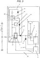
- FIG. 3 illustrates a circuit configuration according to a second embodiment of the present invention
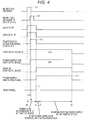
- FIG. 4 illustrates a timing chart to implement FIG. 3
- the circuit configuration includes a signal delay circuit 12, a power storage circuit 13, a second switch circuit 14, a third current direction limiting diode 15, a fourth current direction limiting diode 16, and a delayed-momentary-switch-signal transmission line 17, in addition to the circuit configuration of Fig. 1 .
- the signal delay circuit 12 is a circuit such as an RC circuit formed by, for example, a resistor and a capacitor to delay rising timing of a pulse caused by a potential difference between on and off of the momentary switch 1. In other words, the signal delay circuit 12 delays an input signal from outside.
- the power storage circuit 13 is a circuit, such as a capacitor element, for temporarily supplying power to the D-FF 3 when the second switch circuit 14 is turned off.
- the second switch circuit 14 is a switch circuit for controlling power supply to the D-FF 3.
- the second switch circuit 14 (second switch) includes a second control terminal 14a and turns on/off power supplied to the power-supply activation device 2 in accordance with the potential of the second control terminal 14a.
- An external-input transmission signal line 19 (third signal line) transmits an input signal from outside to the second control terminal 14a.
- the third current direction limiting diode 15 is an element placed between the second switch circuit 14 and a portion between the signal delay circuit 12 and the momentary switch 1 located on the outside. Thus, current flowing to the second switch circuit 14 is prevented from flowing back to both of the signal delay circuit 12 and the momentary switch 1 located on the outside.
- the fourth current direction limiting diode 16 is an element placed between the second switch circuit 14 and a portion between the output Q of the D-FF 3 and the first current direction limiting diode 4. Thus, current flowing to the second switch circuit 14 is prevented from flowing back to both of the output Q of the D-FF 3 and the first current direction limiting diode 4.
- the delayed-momentary-switch-signal transmission line 17 is a signal line for transmitting a pulse signal from the momentary switch 1 delayed by the signal delay circuit 12, to the clock input portion CLK of the D-FF 3.
- the D-FF 3 (logic circuit) holds and outputs a power-supply activation signal in synchronization with a delayed input signal, and resets the held power-supply activation signal in synchronization with a reset signal.
- the potential V2 of the output Q of the D-FF 3 turns on the first switch circuit 6 and the second switch circuit 14 to supply power to the power supply IC 7 and the arithmetic device 8, as in the first embodiment descried above.
- the output Q of the D-FF 3 turns on the second switch circuit 14, the power supply to the D-FF 3 continues even after the momentary switch 1 is opened.
- a power-supply-activation-device output feedback signal line 20 (fourth signal line) transmits the power-supply activation signal output from the D-FF 3 (logic circuit) to the second control terminal 14a.
- the arithmetic device 8 activated by receiving power from the power supply IC 7 maintains the power supply from the power supply device 5 by outputting a power supply maintaining signal.
- the reset signal is output to the D-FF 3 (t2 ⁇ t ⁇ t3) after the arithmetic device 8 is activated, the output Q of the D-FF 3 is reset, and when the second switch circuit 14 is turned off, output and holding (power-supply activation signal) in the power-supply activation device 2 is reset and power supply to an internal circuit of the power-supply activation device 2 is also stopped.
- the second switch circuit 14 turns on power supplied to the power-supply activation device 2. Furthermore, when both of the input signal from outside and the power-supply activation signal are not applied to the second control terminal 14a, the second switch circuit 14 turns off power supplied to the power-supply activation device 2.
- power supply to the power-supply activation device 2 which is unnecessary when the power supply device 5 and the arithmetic device 8 are activated is stopped to reduce current consumption during monitoring trigger from outside or being on standby, in addition to the effects of the first embodiment.
- the present invention may be applied to an electronic control device that performs control as described below when a refuel request switch (momentary switch) is pressed.
- the electronic control device controls an actuator or the like to open a control valve disposed between a fuel tank and a canister (fuel evaporative gas emission preventing device), release an evaporated gas to the canister, and open a fuel cap when the pressure of the fuel tank becomes substantially 0 kPa (when the pressure of the fuel tank becomes equal to or less than a predetermined threshold value).
- a control valve disposed between a fuel tank and a canister (fuel evaporative gas emission preventing device)
- the electronic control device controls an actuator or the like to open a control valve disposed between a fuel tank and a canister (fuel evaporative gas emission preventing device), release an evaporated gas to the canister, and open a fuel cap when the pressure of the fuel tank becomes substantially 0 kPa (when the pressure of the fuel tank becomes equal to or less than a predetermined threshold value).
- the electronic control device can also reduce power consumption of the power-supply activation device while maintaining the drive of the power supply device. Furthermore, even though an engine is stopped (ignition switch is turned off) as in refueling and the power of the electronic control device is off, the electronic control device can be activated.
- the present invention may be applied to an electronic control device that performs control as described below when a signal from a detection switch for detecting opening of a fuel supply lid is input.
- the electronic control device opens a control valve disposed between a fuel tank and a canister to cause the canister to adsorb an evaporated gas.
- an evaporation check valve may be provided in a fuel nozzle guide. Thus, it is possible to prevent the evaporated fuel from being released into the atmosphere.
- the electronic control device can also reduce power consumption of the power-supply activation device while maintaining the drive of the power supply device.
- the electronic control device is a digital computer
- the current consumption thereof increases, but according to the present application example, it is not necessary to cause the electronic control device (digital computer) to wait to perform the above control. Therefore, the current consumption thereof can be reduced.
- the present invention is not limited to the above embodiments, and can include various alterations and modifications.
- the above embodiments are described in detail for ease of understanding the present invention, and therefore, the present invention is not necessarily limited to a configuration including all of the configurations described above.
- part of a configuration of an embodiment can be replaced with a configuration of another embodiment, and a configuration of an embodiment can be added to a configuration of another embodiment.
- additions, eliminations, or substitutions of another configuration may be made.
- the D-FF is used, but another logic circuit may be used.
- configurations, functions, or the like described above may be partially or wholly achieved by hardware, such as a designed integrated circuit.
- the configurations, functions, or the like described above may be achieved with software by interpreting and executing programs to achieve functions by a processor (arithmetic device).
- Information such as a program, a table, a file, or the like that achieves each function can be stored in a recording device, such as a memory device, a hard disk, or a solid state drive (SSD), or a recording medium, such as an IC card, an SD card, or a DVD.
- a recording device such as a memory device, a hard disk, or a solid state drive (SSD), or a recording medium, such as an IC card, an SD card, or a DVD.
- the embodiments of the present invention may include the following aspects.
- unnecessary operation of the power-supply activation device can be stopped after the power supply device and the arithmetic device are activated, and unnecessary current consumption can be reduced.
- separating the functions of the power-supply activation device and the power supply maintaining device enables resetting the power-supply activation device alone, and resetting the power-supply activation device while maintaining the power supply to the system enables reduction of current consumption caused by the power-supply activation device.
Landscapes
- Engineering & Computer Science (AREA)
- Theoretical Computer Science (AREA)
- Physics & Mathematics (AREA)
- General Engineering & Computer Science (AREA)
- General Physics & Mathematics (AREA)
- Power Sources (AREA)
Abstract
Description
- The present invention relates to an electronic control device.
- A technique is known to turn on/off power supplied to a system or the like by using a flip-flop (hereinafter referred to as F/F or FF) (e.g., see
PTLs 1 to 3). - In
PTL 1, "a state detection F/F outputs a switch detection signal of H-level to a CPU by switching operation in turning on or off power as the first trigger. A power control F/F changes a power supply control signal to an H-level by the switching operation as the first trigger when power is turned on, and when power is turned off, the power control signal is changed to an L-level by reset control (second reset signal) of the CPU. The CPU monitors the state of a chattering monitoring signal. When the CPU detects that the state of the signal is stabilized, the CPU controls the state detection F/F to be reset upon turning on power and controls the power supply control F/F to be reset upon turning off power, changing the levels of the state detection F/F and the power supply control F/F to the L level". -
PTL 2 describes "a power supply activation circuit includes a D-flip-flop with a reset function disposed between anoperation switch SW 1 and a DC-DC converter". - In
PTL 3, "a latch circuit transmits an activation signal by pressing of a push button switch, and a central processing unit (CPU) is activated by the activation signal to execute predetermined processing. Chattering occurs when the push button switch is pushed or released, but the CPU resets the latch circuit after a predetermined time elapses from when the predetermined process is finished". -
- PTL 1:
JP 1997-222938 A - PTL 2:
JP H05-205352 A - PTL 3:
JP H06-21785 A - In such a technique as disclosed in
PTL 1, a holding circuit such as a D-FF with reset has both functions of a power-supply activation device and a power supply maintaining device for a power supply device. Thus, power supply for the power supply device is stopped in conjunction with resetting the holding circuit. For this reason, it is necessary to continuously operate the holding circuit while the power supply device supplies power, and the holding circuit always consumes current during power is supplied from the power supply device. - In such a technique as disclosed in
PTL 2 as well, as described above, since a holding circuit has both functions of a power-supply activation device and a power supply maintaining device for a power supply device, the holding circuit always consumes current during power is supplied. - In such a technique as disclosed in
PTL 3, since reset timing of a holding circuit is determined by a timer or the like, it is not possible to reset the holding circuit by an external factor. - An object of the present invention is to provide an electronic control device configured to reduce power consumption of a power-supply activation device while maintaining driving of a power supply device.
- In order to achieve the above object, the present invention includes an arithmetic device, a power supply device for supplying power to the arithmetic device, a power-supply activation device for activating the power supply device, a first signal line for transmitting a power supply drive maintaining signal for maintaining drive of the power supply device, from the arithmetic device to the power supply device, and a second signal line for transmitting, from the arithmetic device to the power-supply activation device, a reset signal for resetting the power-supply activation device.
- According to the present invention, it is possible to reduce the power consumption of the power-supply activation device while maintaining the drive of the power supply device. Problems, configurations, and effects other than those in the above description will be made clear in the following description of the embodiments.
-
-
FIG. 1 is a diagram illustrating a circuit configuration according to a first embodiment of the present invention. -
FIG. 2 is a timing chart according to the first embodiment of the present invention. -
FIG. 3 is a diagram illustrating a circuit configuration according to a second embodiment of the present invention. -
FIG. 4 is a timing chart according to the second embodiment of the present invention. - Hereinafter, the configuration and operation of an electronic control device according to the first and second embodiments of the present invention will be described with reference to the drawings. In the drawings, the same reference numerals denote the same portions.
-
FIG. 1 illustrates a circuit configuration of a control unit 18 (the electronic control device) according to a first embodiment of the present invention, andFIG. 2 is a timing chart to implementFIG. 1 . - When a
momentary switch 1 outside thecontrol unit 18 is turned on (timing t = t0,FIG. 2 ), potential V1 upstream of themomentary switch 1 is applied to a clock input portion CLK of a D-FF (D type flip-flop) 3 while themomentary switch 1 is turned on (t0 ≤ t ≤ t1). At this time, since a data input portion D of the D-FF 3 is connected to a power supply, the potential V1 generated from themomentary switch 1 is recognized as a clock by the clock input portion CLK of the D-FF 3 and data is latched, and an output Q of the D-FF 3 is held at a constant potential V2. - In other words, a power-
supply activation device 2 outputs a power-supply activation signal for activating apower supply device 5, to thepower supply device 5, on the basis of the potential V1 (input signal from outside) generated by themomentary switch 1. Specifically, the power-supply activation device 2 includes the D-FF 3 (logic circuit) for holding and outputting the power-supply activation signal in synchronization with an input signal from outside, and resetting the held power-supply activation signal in synchronism with a reset signal. - Here, even after the
momentary switch 1 is turned off (t1 ≤ t), the potential of the output Q does not change unless the D-FF 3 is reset or power supply to the D-FF 3 is stopped. The output Q of the D-FF 3 is connected to afirst switch circuit 6 which is a constituent portion of thepower supply device 5 via a first currentdirection limiting diode 4, and when the output Q of the D-FF 3 is the constant potential V2 (t = t0), a switch of thefirst switch circuit 6 is turned on, and power is supplied to apower supply IC 7. In this way, the power-supply activation device 2 activates thepower supply device 5. - When the
first switch circuit 6 is turned on, the power supply IC 7 receives power supply, and the power supply IC 7 supplies the power (electric power) to anarithmetic device 8. In other words, thepower supply device 5 supplies power to thearithmetic device 8 during a period in which the power-supply activation signal is input. - The
arithmetic device 8 activated by receiving power supply from thepower supply IC 7 changes a power supply maintainingsignal line 9 for connecting thearithmetic device 8 and thefirst switch circuit 6 via a second currentdirection limiting diode 10, to potential V3 (for example, V3 = V2 is possible) for turning on thefirst switch circuit 6, that is, thearithmetic device 8 outputs the power supply maintaining signal (t = t2). Thus, power supply from thepower supply device 5 is maintained by the arithmetic device 8 (t2 ≤ t ≤ t4). - In other words, the power supply maintaining signal line 9 (first signal line) transmits the power supply maintaining signal (power supply drive maintaining signal) for maintaining drive of the
power supply device 5, from thearithmetic device 8 to thepower supply device 5. Thepower supply device 5 supplies electric power to thearithmetic device 8 during a period in which the power supply maintaining signal (power supply drive maintaining signal) is input. More specifically, thepower supply device 5 includes a first switch circuit 6 (first switch) including afirst control terminal 6a to which the power-supply activation signal and the power supply maintaining signal (power supply drive maintaining signal) are applied to turn on/off electric power supplied to thepower supply device 5 in accordance with the potential of thefirst control terminal 6a. - The
arithmetic device 8 and a reset R of the D-FF 3 are connected by areset signal line 11, and thearithmetic device 8 maintaining the operation of thepower supply device 5 then uses thereset signal line 11 to output a reset signal to the D-FF 3 (t2 ≤ t ≤ t3), and resets a holding signal (power-supply activation signal) in the power-supply activation device 2. - In other words, the reset signal line 11 (second signal line) transmits the reset signal for resetting the power-
supply activation device 2 from thearithmetic device 8 to the power-supply activation device 2. When the reset signal is input, the power-supply activation device 2 stops to output the power-supply activation signal. Thearithmetic device 8 activated with power supplied from thepower supply device 5, outputs a power supply maintaining signal (power supply drive maintaining signal) to thepower supply device 5 and outputs the reset signal to the power-supply activation device 2. - The first current
direction limiting diode 4 and the second currentdirection limiting diode 10 are elements for preventing current from flowing back to the output Q of the D-FF 3 and to thearithmetic device 8, respectively. - In the present embodiment, the device is required to activate the
power supply device 5 andarithmetic device 8 of thecontrol unit 18, which are stopped, by the trigger from outside (from the momentary switch 1). The device is on standby while monitoring the trigger from outside by only driving the power-supply activation device 2, and when thepower supply device 5 and thearithmetic device 8 are activated, the holding signal (power-supply activation signal) in the power-supply activation device 2 becomes unnecessary and is reset. Therefore, the current consumption of the power-supply activation device 2 can be reduced. - As described above, according to the present embodiment, it is possible to reduce the power consumption of the power-
supply activation device 2 while maintaining the drive of thepower supply device 5. -
FIG. 3 illustrates a circuit configuration according to a second embodiment of the present invention, andFIG. 4 illustrates a timing chart to implementFIG. 3 . The circuit configuration includes asignal delay circuit 12, apower storage circuit 13, asecond switch circuit 14, a third currentdirection limiting diode 15, a fourth currentdirection limiting diode 16, and a delayed-momentary-switch-signal transmission line 17, in addition to the circuit configuration ofFig. 1 . - The
signal delay circuit 12 is a circuit such as an RC circuit formed by, for example, a resistor and a capacitor to delay rising timing of a pulse caused by a potential difference between on and off of themomentary switch 1. In other words, thesignal delay circuit 12 delays an input signal from outside. - The
power storage circuit 13 is a circuit, such as a capacitor element, for temporarily supplying power to the D-FF 3 when thesecond switch circuit 14 is turned off. - The
second switch circuit 14 is a switch circuit for controlling power supply to the D-FF 3. In other words, the second switch circuit 14 (second switch) includes asecond control terminal 14a and turns on/off power supplied to the power-supply activation device 2 in accordance with the potential of thesecond control terminal 14a. An external-input transmission signal line 19 (third signal line) transmits an input signal from outside to thesecond control terminal 14a. - The third current
direction limiting diode 15 is an element placed between thesecond switch circuit 14 and a portion between thesignal delay circuit 12 and themomentary switch 1 located on the outside. Thus, current flowing to thesecond switch circuit 14 is prevented from flowing back to both of thesignal delay circuit 12 and themomentary switch 1 located on the outside. - The fourth current
direction limiting diode 16 is an element placed between thesecond switch circuit 14 and a portion between the output Q of the D-FF 3 and the first currentdirection limiting diode 4. Thus, current flowing to thesecond switch circuit 14 is prevented from flowing back to both of the output Q of the D-FF 3 and the first currentdirection limiting diode 4. - The delayed-momentary-switch-
signal transmission line 17 is a signal line for transmitting a pulse signal from themomentary switch 1 delayed by thesignal delay circuit 12, to the clock input portion CLK of the D-FF 3. - When the
momentary switch 1 located outside thecontrol unit 18 is turned on (timing t = t0,FIG. 4 ), potential V1 upstream of themomentary switch 1 is applied to thesignal delay circuit 12 and thesecond switch circuit 14 while themomentary switch 1 is turned on (t0 ≤ t ≤ t1). At this time, when a switch of thesecond switch circuit 14 is turned on by the potential of themomentary switch 1, power is supplied to thepower storage circuit 13, Vcc and the data input portion D of the D-FF 3,. - Furthermore, the potential V1 upstream of the
momentary switch 1 is applied to the clock input portion CLK of the D-FF 3 at timing (t = t10) delayed from the timing of turning on the switch of thesecond switch circuit 14 by thesignal delay circuit 12. Since the power is already supplied to the Vcc and the data input portion D of the D-FF 3 as described above, the potential generated by themomentary switch 1 is recognized as a clock by the clock input portion CLK of the D-FF 3 and data is latched, and the output Q of the D-FF 3 becomes a constant potential V2, as in the first embodiment. - In other words, the D-FF 3 (logic circuit) holds and outputs a power-supply activation signal in synchronization with a delayed input signal, and resets the held power-supply activation signal in synchronization with a reset signal.
- The potential V2 of the output Q of the D-
FF 3 turns on thefirst switch circuit 6 and thesecond switch circuit 14 to supply power to thepower supply IC 7 and thearithmetic device 8, as in the first embodiment descried above. In addition, since the output Q of the D-FF 3 turns on thesecond switch circuit 14, the power supply to the D-FF 3 continues even after themomentary switch 1 is opened. - In other words, a power-supply-activation-device output feedback signal line 20 (fourth signal line) transmits the power-supply activation signal output from the D-FF 3 (logic circuit) to the
second control terminal 14a. - As in the first embodiment, the
arithmetic device 8 activated by receiving power from thepower supply IC 7 maintains the power supply from thepower supply device 5 by outputting a power supply maintaining signal. When the reset signal is output to the D-FF 3 (t2 ≤ t ≤ t3) after thearithmetic device 8 is activated, the output Q of the D-FF 3 is reset, and when thesecond switch circuit 14 is turned off, output and holding (power-supply activation signal) in the power-supply activation device 2 is reset and power supply to an internal circuit of the power-supply activation device 2 is also stopped. - In other words, when at least one of an input signal from outside and the power-supply activation signal is applied to the
second control terminal 14a, the second switch circuit 14 (second switch) turns on power supplied to the power-supply activation device 2. Furthermore, when both of the input signal from outside and the power-supply activation signal are not applied to thesecond control terminal 14a, thesecond switch circuit 14 turns off power supplied to the power-supply activation device 2. - In the present embodiment, power supply to the power-
supply activation device 2 which is unnecessary when thepower supply device 5 and thearithmetic device 8 are activated is stopped to reduce current consumption during monitoring trigger from outside or being on standby, in addition to the effects of the first embodiment. - As described above, according to the present embodiment, it is possible to reduce the power consumption of the power-
supply activation device 2 while maintaining the drive of thepower supply device 5. - For example, the present invention may be applied to an electronic control device that performs control as described below when a refuel request switch (momentary switch) is pressed.
- The electronic control device controls an actuator or the like to open a control valve disposed between a fuel tank and a canister (fuel evaporative gas emission preventing device), release an evaporated gas to the canister, and open a fuel cap when the pressure of the fuel tank becomes substantially 0 kPa (when the pressure of the fuel tank becomes equal to or less than a predetermined threshold value). Thus, it is possible to prevent the evaporated fuel from being released into the atmosphere.
- In this application example, the electronic control device can also reduce power consumption of the power-supply activation device while maintaining the drive of the power supply device. Furthermore, even though an engine is stopped (ignition switch is turned off) as in refueling and the power of the electronic control device is off, the electronic control device can be activated.
- For example, the present invention may be applied to an electronic control device that performs control as described below when a signal from a detection switch for detecting opening of a fuel supply lid is input.
- The electronic control device opens a control valve disposed between a fuel tank and a canister to cause the canister to adsorb an evaporated gas. Note that an evaporation check valve may be provided in a fuel nozzle guide. Thus, it is possible to prevent the evaporated fuel from being released into the atmosphere.
- In this application example, the electronic control device can also reduce power consumption of the power-supply activation device while maintaining the drive of the power supply device. In particular, when the electronic control device is a digital computer, the current consumption thereof increases, but according to the present application example, it is not necessary to cause the electronic control device (digital computer) to wait to perform the above control. Therefore, the current consumption thereof can be reduced.
- Note that the present invention is not limited to the above embodiments, and can include various alterations and modifications. For example, the above embodiments are described in detail for ease of understanding the present invention, and therefore, the present invention is not necessarily limited to a configuration including all of the configurations described above. Furthermore, part of a configuration of an embodiment can be replaced with a configuration of another embodiment, and a configuration of an embodiment can be added to a configuration of another embodiment. Still furthermore, for part of the configurations of the respective embodiments, additions, eliminations, or substitutions of another configuration may be made.
- In the above embodiment, the D-FF is used, but another logic circuit may be used.
- In addition, the configurations, functions, or the like described above may be partially or wholly achieved by hardware, such as a designed integrated circuit. In addition, the configurations, functions, or the like described above may be achieved with software by interpreting and executing programs to achieve functions by a processor (arithmetic device). Information such as a program, a table, a file, or the like that achieves each function can be stored in a recording device, such as a memory device, a hard disk, or a solid state drive (SSD), or a recording medium, such as an IC card, an SD card, or a DVD.
- The embodiments of the present invention may include the following aspects.
- (1) An electronic control device including an arithmetic device, a power supply device for supplying power to the arithmetic device, a power-supply activation device for activating the power supply device, a power supply drive maintaining signal line for transmitting a power supply drive maintaining signal from the arithmetic device to the power supply device, and a reset signal line for transmitting a reset signal from the arithmetic device to the power-supply activation device.
- (2) An electronic control device including an arithmetic device, a power supply device for supplying power to the arithmetic device, and a power-supply activation device for activating the power supply device, in which the power-supply activation device outputs an activation signal to the power supply device on the basis of an input from outside, the power supply device supplies power to the arithmetic device when an activation signal is input, the arithmetic device outputs a power supply drive maintaining signal to the power supply device when power is supplied from the power supply device, and the arithmetic device outputs a reset signal to the power-supply activation device after activation.
- (3) The electronic control device according to (2), in which a D-FF with reset or an FF is used for the power-supply activation device.
- (4) The electronic control device according to (2), further including a signal delay circuit for delaying an input signal from outside, a switch circuit for switching power supply and stop of the power supply to the power-supply activation device, and an external-input transmission signal line for transmitting an input from outside to the switch circuit, and a power-supply-activation-device output feedback signal line for transmitting an output from the power-supply activation device to the switch circuit, in which the switch circuit supplies power to the power-supply activation device on the basis of an input from outside, and the delay circuit inputs a delayed input signal from outside to the power supply activation device and outputs, on the basis of an input from outside via the delay circuit, an activation signal to the power supply device and a switch-on signal to the switch circuit by using the power-supply-activation-device output feedback signal line, in which the switch circuit continues power supply to the power supply activation circuit by using the switch-on signal when there is no input from outside, and power supply to the power supply activation circuit is stopped by turning off the switch circuit by using the reset signal.
- According to the above embodiments (1) to (4), unnecessary operation of the power-supply activation device can be stopped after the power supply device and the arithmetic device are activated, and unnecessary current consumption can be reduced. In other words, separating the functions of the power-supply activation device and the power supply maintaining device enables resetting the power-supply activation device alone, and resetting the power-supply activation device while maintaining the power supply to the system enables reduction of current consumption caused by the power-supply activation device.
-
- 1 momentary switch
- 2 power-supply activation device
- 3 D-FF
- 4 first current direction limiting diode
- 5 power supply device
- 6 first switch circuit
- 7 power supply IC
- 8 arithmetic device
- 9 power supply maintaining signal line
- 10 second current direction limiting diode
- 11 reset signal line
- 12 signal delay circuit
- 13 power storage circuit
- 14 second switch circuit
- 15 third current direction limiting diode
- 16 fourth current direction limiting diode
- 17 delayed-momentary-switch-signal transmission line
- 18 control unit
- 19 external-input transmission signal line
- 20 power-supply-activation-device output feedback signal line
Claims (7)
- An electronic control device comprising:an arithmetic device;a power supply device which supplies power to the arithmetic device;a power-supply activation device which activates the power supply device;a first signal line which transmits a power supply drive maintaining signal for maintaining drive of the power supply device, from the arithmetic device to the power supply device; anda second signal line which transmits a reset signal for resetting the power-supply activation device, from the arithmetic device to the power-supply activation device.
- The electronic control device according to claim 1, wherein
the power-supply activation device
outputs a power-supply activation signal for activating the power supply device to the power supply device, on the basis of an input signal from outside,
the power supply device
supplies power to the arithmetic device during a period in which the power-supply activation signal is input, and
the arithmetic device
after activation with power supplied from the power supply device, outputs the power supply drive maintaining signal to the power supply device and outputs a reset signal to the power-supply activation device. - The electronic control device according to claim 2, wherein
the power supply device
supplies power to the arithmetic device during a period in which the power supply drive maintaining signal is input. - The electronic control device according to claim 3, wherein
the power-supply activation device
stops output of the power-supply activation signal, when the reset signal is input. - The electronic control device according to claim 2, wherein
the power supply device includes
a first switch which has a first control terminal to which the power-supply activation signal and the power supply drive maintaining signal are applied to turn on/off power supplied to the power supply device in accordance with a potential of the first control terminal. - The electronic control device according to claim 5, wherein
the power-supply activation device includes
a logic circuit which holds and outputs the power-supply activation signal in synchronization with an input signal from outside and resets the held power-supply activation signal in synchronization with the reset signal. - The electronic control device according to claim 5, wherein
the power-supply activation device includes:a second switch which has a second control terminal to turn on/off power supplied to the power-supply activation device in accordance with potential of the second control terminal;a signal delay circuit which delays the input signal from outside;a logic circuit which holds and outputs the power-supply activation signal in synchronization with the delayed input signal and resets the held power-supply activation signal in synchronization with the reset signal;a third signal line which transmits the input signal from outside to the second control terminal; anda fourth signal line which transmits the power-supply activation signal output from the logic circuit to the second control terminal, andthe second switchturns on power supplied to the power-supply activation device when at least one of the input signal from outside and the power-supply activation signal is applied to the second control terminal, andturns off power supplied to the power-supply activation device when both the input signal from outside and the power-supply activation signal is not applied to the second control terminal.
Applications Claiming Priority (2)
| Application Number | Priority Date | Filing Date | Title |
|---|---|---|---|
| JP2016144038 | 2016-07-22 | ||
| PCT/JP2017/022992 WO2018016260A1 (en) | 2016-07-22 | 2017-06-22 | Electronic control device |
Publications (3)
| Publication Number | Publication Date |
|---|---|
| EP3489796A1 true EP3489796A1 (en) | 2019-05-29 |
| EP3489796A4 EP3489796A4 (en) | 2020-04-01 |
| EP3489796B1 EP3489796B1 (en) | 2021-02-17 |
Family
ID=60992111
Family Applications (1)
| Application Number | Title | Priority Date | Filing Date |
|---|---|---|---|
| EP17830780.7A Active EP3489796B1 (en) | 2016-07-22 | 2017-06-22 | Electronic control device |
Country Status (5)
| Country | Link |
|---|---|
| US (1) | US10928872B2 (en) |
| EP (1) | EP3489796B1 (en) |
| JP (1) | JP6653760B2 (en) |
| CN (1) | CN109451756B (en) |
| WO (1) | WO2018016260A1 (en) |
Families Citing this family (2)
| Publication number | Priority date | Publication date | Assignee | Title |
|---|---|---|---|---|
| CN111162768B (en) * | 2018-11-07 | 2023-01-31 | 台达电子工业股份有限公司 | Control device and method |
| TWI764813B (en) * | 2021-08-18 | 2022-05-11 | 立積電子股份有限公司 | Driving circuit |
Family Cites Families (14)
| Publication number | Priority date | Publication date | Assignee | Title |
|---|---|---|---|---|
| JPH05205352A (en) * | 1992-01-24 | 1993-08-13 | Sony Corp | Power supply starting circuit |
| JPH0621785A (en) * | 1992-07-03 | 1994-01-28 | Nec Eng Ltd | Chattering preventing system |
| JPH09222938A (en) | 1996-02-14 | 1997-08-26 | Casio Comput Co Ltd | Power control device |
| KR0162599B1 (en) * | 1996-05-07 | 1999-01-15 | 김광호 | Power control system |
| JP4032955B2 (en) | 2002-12-17 | 2008-01-16 | 株式会社日立製作所 | Electronic control unit for automobile |
| US7124005B2 (en) * | 2003-08-07 | 2006-10-17 | Denso Corporation | Electronic control unit having hold circuit and method therefor |
| JP4543946B2 (en) * | 2005-01-28 | 2010-09-15 | アイシン精機株式会社 | Start-up circuit |
| JP5734615B2 (en) * | 2010-10-14 | 2015-06-17 | ラピスセミコンダクタ株式会社 | Inspection apparatus and method |
| JP2014002456A (en) * | 2012-06-15 | 2014-01-09 | Denso Corp | Input signal processing device |
| KR101481243B1 (en) * | 2012-12-28 | 2015-01-09 | 현대자동차주식회사 | System and method for incipient drive of battery charger for green car |
| US9007122B2 (en) * | 2013-06-05 | 2015-04-14 | Via Technologies, Inc. | Digital power gating with state retention |
| JP6066872B2 (en) * | 2013-09-10 | 2017-01-25 | 三菱電機株式会社 | Disk unit |
| US9524007B2 (en) * | 2014-02-04 | 2016-12-20 | Qualcomm Incorporated | Diagnostic systems and methods of finite state machines |
| US10608615B2 (en) * | 2016-01-28 | 2020-03-31 | Samsung Electronics Co., Ltd. | Semiconductor device including retention reset flip-flop |
-
2017
- 2017-06-22 JP JP2018528458A patent/JP6653760B2/en active Active
- 2017-06-22 EP EP17830780.7A patent/EP3489796B1/en active Active
- 2017-06-22 CN CN201780042952.1A patent/CN109451756B/en active Active
- 2017-06-22 WO PCT/JP2017/022992 patent/WO2018016260A1/en not_active Ceased
- 2017-06-22 US US16/317,439 patent/US10928872B2/en active Active
Also Published As
| Publication number | Publication date |
|---|---|
| CN109451756B (en) | 2022-05-13 |
| JPWO2018016260A1 (en) | 2019-04-04 |
| US20190302870A1 (en) | 2019-10-03 |
| EP3489796A4 (en) | 2020-04-01 |
| CN109451756A (en) | 2019-03-08 |
| US10928872B2 (en) | 2021-02-23 |
| EP3489796B1 (en) | 2021-02-17 |
| JP6653760B2 (en) | 2020-02-26 |
| WO2018016260A1 (en) | 2018-01-25 |
Similar Documents
| Publication | Publication Date | Title |
|---|---|---|
| JP5633139B2 (en) | Information equipment | |
| US7765415B2 (en) | Semiconductor integrated circuit | |
| JP2010154294A (en) | Synchronization circuit | |
| US8214674B2 (en) | Integrated circuit having a microcontroller unit and methods of controlling the operation mode thereof | |
| EP3489796B1 (en) | Electronic control device | |
| US8423802B2 (en) | Power scaling module and power scaling unit of an electronic system having a function unit in a standby state which is insensitive to change in frequency or voltage during synchronization | |
| US10719331B2 (en) | Stand-by mode of an electronic circuit | |
| US20030189862A1 (en) | Backup memory control unit with | |
| CN105320028A (en) | Load control backup signal generating circuit | |
| JP5125605B2 (en) | Integrated circuit device having reset control | |
| US9075588B2 (en) | Voltage regulator and control circuit for supplying voltage to a plurality of subcircuits via a chain of switches | |
| CN112394804A (en) | Power supply regulation and control device, computer system and related power supply regulation and control method thereof | |
| US9933839B2 (en) | Computer system and method of operating a computer system | |
| US20090284289A1 (en) | method of implementing power-on-reset in power switches | |
| JP6066872B2 (en) | Disk unit | |
| JP7121741B2 (en) | logic circuit, sequential circuit, power control circuit, switching power supply | |
| US9887693B2 (en) | Clock selection circuit and power supply device equipped with the same | |
| US9802560B2 (en) | Electronic circuit | |
| US12452980B2 (en) | Power control of a light animation performed on a light module | |
| JP2007157199A (en) | Semiconductor device | |
| JP2012116237A (en) | Electric control apparatus and initialization method | |
| JPH11220871A (en) | Power supply | |
| CN109074338B (en) | Integrated circuit device | |
| KR101080720B1 (en) | Circuit to guarantee operating PLL of central processing unit | |
| JP2006350930A (en) | Control circuit and information processor |
Legal Events
| Date | Code | Title | Description |
|---|---|---|---|
| STAA | Information on the status of an ep patent application or granted ep patent |
Free format text: STATUS: THE INTERNATIONAL PUBLICATION HAS BEEN MADE |
|
| PUAI | Public reference made under article 153(3) epc to a published international application that has entered the european phase |
Free format text: ORIGINAL CODE: 0009012 |
|
| STAA | Information on the status of an ep patent application or granted ep patent |
Free format text: STATUS: REQUEST FOR EXAMINATION WAS MADE |
|
| 17P | Request for examination filed |
Effective date: 20190222 |
|
| AK | Designated contracting states |
Kind code of ref document: A1 Designated state(s): AL AT BE BG CH CY CZ DE DK EE ES FI FR GB GR HR HU IE IS IT LI LT LU LV MC MK MT NL NO PL PT RO RS SE SI SK SM TR |
|
| AX | Request for extension of the european patent |
Extension state: BA ME |
|
| DAV | Request for validation of the european patent (deleted) | ||
| DAX | Request for extension of the european patent (deleted) | ||
| A4 | Supplementary search report drawn up and despatched |
Effective date: 20200227 |
|
| RIC1 | Information provided on ipc code assigned before grant |
Ipc: G06F 1/26 20060101AFI20200222BHEP Ipc: G06F 1/32 20190101ALI20200222BHEP |
|
| STAA | Information on the status of an ep patent application or granted ep patent |
Free format text: STATUS: EXAMINATION IS IN PROGRESS |
|
| 17Q | First examination report despatched |
Effective date: 20200616 |
|
| GRAP | Despatch of communication of intention to grant a patent |
Free format text: ORIGINAL CODE: EPIDOSNIGR1 |
|
| STAA | Information on the status of an ep patent application or granted ep patent |
Free format text: STATUS: GRANT OF PATENT IS INTENDED |
|
| INTG | Intention to grant announced |
Effective date: 20201020 |
|
| GRAS | Grant fee paid |
Free format text: ORIGINAL CODE: EPIDOSNIGR3 |
|
| GRAA | (expected) grant |
Free format text: ORIGINAL CODE: 0009210 |
|
| STAA | Information on the status of an ep patent application or granted ep patent |
Free format text: STATUS: THE PATENT HAS BEEN GRANTED |
|
| AK | Designated contracting states |
Kind code of ref document: B1 Designated state(s): AL AT BE BG CH CY CZ DE DK EE ES FI FR GB GR HR HU IE IS IT LI LT LU LV MC MK MT NL NO PL PT RO RS SE SI SK SM TR |
|
| REG | Reference to a national code |
Ref country code: GB Ref legal event code: FG4D |
|
| REG | Reference to a national code |
Ref country code: CH Ref legal event code: EP |
|
| REG | Reference to a national code |
Ref country code: DE Ref legal event code: R096 Ref document number: 602017032937 Country of ref document: DE |
|
| REG | Reference to a national code |
Ref country code: AT Ref legal event code: REF Ref document number: 1362310 Country of ref document: AT Kind code of ref document: T Effective date: 20210315 |
|
| REG | Reference to a national code |
Ref country code: IE Ref legal event code: FG4D |
|
| REG | Reference to a national code |
Ref country code: LT Ref legal event code: MG9D |
|
| REG | Reference to a national code |
Ref country code: NL Ref legal event code: MP Effective date: 20210217 |
|
| PG25 | Lapsed in a contracting state [announced via postgrant information from national office to epo] |
Ref country code: GR Free format text: LAPSE BECAUSE OF FAILURE TO SUBMIT A TRANSLATION OF THE DESCRIPTION OR TO PAY THE FEE WITHIN THE PRESCRIBED TIME-LIMIT Effective date: 20210518 Ref country code: FI Free format text: LAPSE BECAUSE OF FAILURE TO SUBMIT A TRANSLATION OF THE DESCRIPTION OR TO PAY THE FEE WITHIN THE PRESCRIBED TIME-LIMIT Effective date: 20210217 Ref country code: HR Free format text: LAPSE BECAUSE OF FAILURE TO SUBMIT A TRANSLATION OF THE DESCRIPTION OR TO PAY THE FEE WITHIN THE PRESCRIBED TIME-LIMIT Effective date: 20210217 Ref country code: NO Free format text: LAPSE BECAUSE OF FAILURE TO SUBMIT A TRANSLATION OF THE DESCRIPTION OR TO PAY THE FEE WITHIN THE PRESCRIBED TIME-LIMIT Effective date: 20210517 Ref country code: PT Free format text: LAPSE BECAUSE OF FAILURE TO SUBMIT A TRANSLATION OF THE DESCRIPTION OR TO PAY THE FEE WITHIN THE PRESCRIBED TIME-LIMIT Effective date: 20210617 Ref country code: BG Free format text: LAPSE BECAUSE OF FAILURE TO SUBMIT A TRANSLATION OF THE DESCRIPTION OR TO PAY THE FEE WITHIN THE PRESCRIBED TIME-LIMIT Effective date: 20210517 Ref country code: LT Free format text: LAPSE BECAUSE OF FAILURE TO SUBMIT A TRANSLATION OF THE DESCRIPTION OR TO PAY THE FEE WITHIN THE PRESCRIBED TIME-LIMIT Effective date: 20210217 |
|
| REG | Reference to a national code |
Ref country code: AT Ref legal event code: MK05 Ref document number: 1362310 Country of ref document: AT Kind code of ref document: T Effective date: 20210217 |
|
| PG25 | Lapsed in a contracting state [announced via postgrant information from national office to epo] |
Ref country code: NL Free format text: LAPSE BECAUSE OF FAILURE TO SUBMIT A TRANSLATION OF THE DESCRIPTION OR TO PAY THE FEE WITHIN THE PRESCRIBED TIME-LIMIT Effective date: 20210217 Ref country code: RS Free format text: LAPSE BECAUSE OF FAILURE TO SUBMIT A TRANSLATION OF THE DESCRIPTION OR TO PAY THE FEE WITHIN THE PRESCRIBED TIME-LIMIT Effective date: 20210217 Ref country code: LV Free format text: LAPSE BECAUSE OF FAILURE TO SUBMIT A TRANSLATION OF THE DESCRIPTION OR TO PAY THE FEE WITHIN THE PRESCRIBED TIME-LIMIT Effective date: 20210217 Ref country code: PL Free format text: LAPSE BECAUSE OF FAILURE TO SUBMIT A TRANSLATION OF THE DESCRIPTION OR TO PAY THE FEE WITHIN THE PRESCRIBED TIME-LIMIT Effective date: 20210217 Ref country code: SE Free format text: LAPSE BECAUSE OF FAILURE TO SUBMIT A TRANSLATION OF THE DESCRIPTION OR TO PAY THE FEE WITHIN THE PRESCRIBED TIME-LIMIT Effective date: 20210217 |
|
| REG | Reference to a national code |
Ref country code: DE Ref legal event code: R081 Ref document number: 602017032937 Country of ref document: DE Owner name: HITACHI ASTEMO, LTD., HITACHINAKA-SHI, JP Free format text: FORMER OWNER: HITACHI AUTOMOTIVE SYSTEMS, LTD., HITACHINAKA-SHI, IBARAKI, JP |
|
| PG25 | Lapsed in a contracting state [announced via postgrant information from national office to epo] |
Ref country code: IS Free format text: LAPSE BECAUSE OF FAILURE TO SUBMIT A TRANSLATION OF THE DESCRIPTION OR TO PAY THE FEE WITHIN THE PRESCRIBED TIME-LIMIT Effective date: 20210617 |
|
| PG25 | Lapsed in a contracting state [announced via postgrant information from national office to epo] |
Ref country code: CZ Free format text: LAPSE BECAUSE OF FAILURE TO SUBMIT A TRANSLATION OF THE DESCRIPTION OR TO PAY THE FEE WITHIN THE PRESCRIBED TIME-LIMIT Effective date: 20210217 Ref country code: EE Free format text: LAPSE BECAUSE OF FAILURE TO SUBMIT A TRANSLATION OF THE DESCRIPTION OR TO PAY THE FEE WITHIN THE PRESCRIBED TIME-LIMIT Effective date: 20210217 Ref country code: SM Free format text: LAPSE BECAUSE OF FAILURE TO SUBMIT A TRANSLATION OF THE DESCRIPTION OR TO PAY THE FEE WITHIN THE PRESCRIBED TIME-LIMIT Effective date: 20210217 Ref country code: AT Free format text: LAPSE BECAUSE OF FAILURE TO SUBMIT A TRANSLATION OF THE DESCRIPTION OR TO PAY THE FEE WITHIN THE PRESCRIBED TIME-LIMIT Effective date: 20210217 |
|
| REG | Reference to a national code |
Ref country code: DE Ref legal event code: R097 Ref document number: 602017032937 Country of ref document: DE |
|
| PG25 | Lapsed in a contracting state [announced via postgrant information from national office to epo] |
Ref country code: DK Free format text: LAPSE BECAUSE OF FAILURE TO SUBMIT A TRANSLATION OF THE DESCRIPTION OR TO PAY THE FEE WITHIN THE PRESCRIBED TIME-LIMIT Effective date: 20210217 Ref country code: SK Free format text: LAPSE BECAUSE OF FAILURE TO SUBMIT A TRANSLATION OF THE DESCRIPTION OR TO PAY THE FEE WITHIN THE PRESCRIBED TIME-LIMIT Effective date: 20210217 Ref country code: RO Free format text: LAPSE BECAUSE OF FAILURE TO SUBMIT A TRANSLATION OF THE DESCRIPTION OR TO PAY THE FEE WITHIN THE PRESCRIBED TIME-LIMIT Effective date: 20210217 |
|
| PLBE | No opposition filed within time limit |
Free format text: ORIGINAL CODE: 0009261 |
|
| STAA | Information on the status of an ep patent application or granted ep patent |
Free format text: STATUS: NO OPPOSITION FILED WITHIN TIME LIMIT |
|
| 26N | No opposition filed |
Effective date: 20211118 |
|
| PG25 | Lapsed in a contracting state [announced via postgrant information from national office to epo] |
Ref country code: ES Free format text: LAPSE BECAUSE OF FAILURE TO SUBMIT A TRANSLATION OF THE DESCRIPTION OR TO PAY THE FEE WITHIN THE PRESCRIBED TIME-LIMIT Effective date: 20210217 Ref country code: AL Free format text: LAPSE BECAUSE OF FAILURE TO SUBMIT A TRANSLATION OF THE DESCRIPTION OR TO PAY THE FEE WITHIN THE PRESCRIBED TIME-LIMIT Effective date: 20210217 Ref country code: MC Free format text: LAPSE BECAUSE OF FAILURE TO SUBMIT A TRANSLATION OF THE DESCRIPTION OR TO PAY THE FEE WITHIN THE PRESCRIBED TIME-LIMIT Effective date: 20210217 |
|
| REG | Reference to a national code |
Ref country code: CH Ref legal event code: PL |
|
| GBPC | Gb: european patent ceased through non-payment of renewal fee |
Effective date: 20210622 |
|
| PG25 | Lapsed in a contracting state [announced via postgrant information from national office to epo] |
Ref country code: SI Free format text: LAPSE BECAUSE OF FAILURE TO SUBMIT A TRANSLATION OF THE DESCRIPTION OR TO PAY THE FEE WITHIN THE PRESCRIBED TIME-LIMIT Effective date: 20210217 |
|
| REG | Reference to a national code |
Ref country code: BE Ref legal event code: MM Effective date: 20210630 |
|
| PG25 | Lapsed in a contracting state [announced via postgrant information from national office to epo] |
Ref country code: LU Free format text: LAPSE BECAUSE OF NON-PAYMENT OF DUE FEES Effective date: 20210622 |
|
| PG25 | Lapsed in a contracting state [announced via postgrant information from national office to epo] |
Ref country code: LI Free format text: LAPSE BECAUSE OF NON-PAYMENT OF DUE FEES Effective date: 20210630 Ref country code: IT Free format text: LAPSE BECAUSE OF FAILURE TO SUBMIT A TRANSLATION OF THE DESCRIPTION OR TO PAY THE FEE WITHIN THE PRESCRIBED TIME-LIMIT Effective date: 20210217 Ref country code: IE Free format text: LAPSE BECAUSE OF NON-PAYMENT OF DUE FEES Effective date: 20210622 Ref country code: GB Free format text: LAPSE BECAUSE OF NON-PAYMENT OF DUE FEES Effective date: 20210622 Ref country code: CH Free format text: LAPSE BECAUSE OF NON-PAYMENT OF DUE FEES Effective date: 20210630 |
|
| PG25 | Lapsed in a contracting state [announced via postgrant information from national office to epo] |
Ref country code: IS Free format text: LAPSE BECAUSE OF FAILURE TO SUBMIT A TRANSLATION OF THE DESCRIPTION OR TO PAY THE FEE WITHIN THE PRESCRIBED TIME-LIMIT Effective date: 20210617 |
|
| PG25 | Lapsed in a contracting state [announced via postgrant information from national office to epo] |
Ref country code: BE Free format text: LAPSE BECAUSE OF NON-PAYMENT OF DUE FEES Effective date: 20210630 |
|
| PG25 | Lapsed in a contracting state [announced via postgrant information from national office to epo] |
Ref country code: CY Free format text: LAPSE BECAUSE OF FAILURE TO SUBMIT A TRANSLATION OF THE DESCRIPTION OR TO PAY THE FEE WITHIN THE PRESCRIBED TIME-LIMIT Effective date: 20210217 |
|
| PG25 | Lapsed in a contracting state [announced via postgrant information from national office to epo] |
Ref country code: HU Free format text: LAPSE BECAUSE OF FAILURE TO SUBMIT A TRANSLATION OF THE DESCRIPTION OR TO PAY THE FEE WITHIN THE PRESCRIBED TIME-LIMIT; INVALID AB INITIO Effective date: 20170622 |
|
| PG25 | Lapsed in a contracting state [announced via postgrant information from national office to epo] |
Ref country code: MK Free format text: LAPSE BECAUSE OF FAILURE TO SUBMIT A TRANSLATION OF THE DESCRIPTION OR TO PAY THE FEE WITHIN THE PRESCRIBED TIME-LIMIT Effective date: 20210217 |
|
| PG25 | Lapsed in a contracting state [announced via postgrant information from national office to epo] |
Ref country code: TR Free format text: LAPSE BECAUSE OF FAILURE TO SUBMIT A TRANSLATION OF THE DESCRIPTION OR TO PAY THE FEE WITHIN THE PRESCRIBED TIME-LIMIT Effective date: 20210217 |
|
| PG25 | Lapsed in a contracting state [announced via postgrant information from national office to epo] |
Ref country code: MT Free format text: LAPSE BECAUSE OF FAILURE TO SUBMIT A TRANSLATION OF THE DESCRIPTION OR TO PAY THE FEE WITHIN THE PRESCRIBED TIME-LIMIT Effective date: 20210217 |
|
| PGFP | Annual fee paid to national office [announced via postgrant information from national office to epo] |
Ref country code: DE Payment date: 20260430 Year of fee payment: 10 |
|
| PGFP | Annual fee paid to national office [announced via postgrant information from national office to epo] |
Ref country code: FR Payment date: 20260511 Year of fee payment: 10 |