EP3489082A1 - Lichtmodul und fahrzeugscheinwerfer - Google Patents
Lichtmodul und fahrzeugscheinwerfer Download PDFInfo
- Publication number
- EP3489082A1 EP3489082A1 EP17204004.0A EP17204004A EP3489082A1 EP 3489082 A1 EP3489082 A1 EP 3489082A1 EP 17204004 A EP17204004 A EP 17204004A EP 3489082 A1 EP3489082 A1 EP 3489082A1
- Authority
- EP
- European Patent Office
- Prior art keywords
- circuit board
- printed circuit
- light module
- spring contact
- contact element
- Prior art date
- Legal status (The legal status is an assumption and is not a legal conclusion. Google has not performed a legal analysis and makes no representation as to the accuracy of the status listed.)
- Granted
Links
- 239000004020 conductor Substances 0.000 claims abstract description 10
- 239000000463 material Substances 0.000 claims description 10
- 229910052751 metal Inorganic materials 0.000 claims description 8
- 239000002184 metal Substances 0.000 claims description 8
- 239000003795 chemical substances by application Substances 0.000 claims description 5
- 239000012530 fluid Substances 0.000 claims description 5
- 239000011248 coating agent Substances 0.000 claims description 3
- 238000000576 coating method Methods 0.000 claims description 3
- 230000003287 optical effect Effects 0.000 description 5
- RYGMFSIKBFXOCR-UHFFFAOYSA-N Copper Chemical compound [Cu] RYGMFSIKBFXOCR-UHFFFAOYSA-N 0.000 description 2
- 150000001875 compounds Chemical class 0.000 description 2
- 229910052802 copper Inorganic materials 0.000 description 2
- 239000010949 copper Substances 0.000 description 2
- 238000009826 distribution Methods 0.000 description 2
- 238000009713 electroplating Methods 0.000 description 2
- 230000002349 favourable effect Effects 0.000 description 2
- 230000017525 heat dissipation Effects 0.000 description 2
- 238000009434 installation Methods 0.000 description 2
- 239000000758 substrate Substances 0.000 description 2
- 229910000639 Spring steel Inorganic materials 0.000 description 1
- 239000000853 adhesive Substances 0.000 description 1
- 230000001070 adhesive effect Effects 0.000 description 1
- 229910052782 aluminium Inorganic materials 0.000 description 1
- XAGFODPZIPBFFR-UHFFFAOYSA-N aluminium Chemical compound [Al] XAGFODPZIPBFFR-UHFFFAOYSA-N 0.000 description 1
- 238000010276 construction Methods 0.000 description 1
- 238000001816 cooling Methods 0.000 description 1
- 230000008878 coupling Effects 0.000 description 1
- 238000010168 coupling process Methods 0.000 description 1
- 238000005859 coupling reaction Methods 0.000 description 1
- 238000000034 method Methods 0.000 description 1
- 239000004065 semiconductor Substances 0.000 description 1
- 229910000679 solder Inorganic materials 0.000 description 1
Images


Classifications
-
- B—PERFORMING OPERATIONS; TRANSPORTING
- B60—VEHICLES IN GENERAL
- B60Q—ARRANGEMENT OF SIGNALLING OR LIGHTING DEVICES, THE MOUNTING OR SUPPORTING THEREOF OR CIRCUITS THEREFOR, FOR VEHICLES IN GENERAL
- B60Q1/00—Arrangement of optical signalling or lighting devices, the mounting or supporting thereof or circuits therefor
- B60Q1/0088—Details of electrical connections
- B60Q1/0094—Arrangement of electronic circuits separated from the light source, e.g. mounting of housings for starter circuits for discharge lamps
-
- F—MECHANICAL ENGINEERING; LIGHTING; HEATING; WEAPONS; BLASTING
- F21—LIGHTING
- F21S—NON-PORTABLE LIGHTING DEVICES; SYSTEMS THEREOF; VEHICLE LIGHTING DEVICES SPECIALLY ADAPTED FOR VEHICLE EXTERIORS
- F21S41/00—Illuminating devices specially adapted for vehicle exteriors, e.g. headlamps
- F21S41/10—Illuminating devices specially adapted for vehicle exteriors, e.g. headlamps characterised by the light source
- F21S41/14—Illuminating devices specially adapted for vehicle exteriors, e.g. headlamps characterised by the light source characterised by the type of light source
- F21S41/141—Light emitting diodes [LED]
-
- F—MECHANICAL ENGINEERING; LIGHTING; HEATING; WEAPONS; BLASTING
- F21—LIGHTING
- F21S—NON-PORTABLE LIGHTING DEVICES; SYSTEMS THEREOF; VEHICLE LIGHTING DEVICES SPECIALLY ADAPTED FOR VEHICLE EXTERIORS
- F21S41/00—Illuminating devices specially adapted for vehicle exteriors, e.g. headlamps
- F21S41/10—Illuminating devices specially adapted for vehicle exteriors, e.g. headlamps characterised by the light source
- F21S41/19—Attachment of light sources or lamp holders
- F21S41/192—Details of lamp holders, terminals or connectors
-
- F—MECHANICAL ENGINEERING; LIGHTING; HEATING; WEAPONS; BLASTING
- F21—LIGHTING
- F21S—NON-PORTABLE LIGHTING DEVICES; SYSTEMS THEREOF; VEHICLE LIGHTING DEVICES SPECIALLY ADAPTED FOR VEHICLE EXTERIORS
- F21S45/00—Arrangements within vehicle lighting devices specially adapted for vehicle exteriors, for purposes other than emission or distribution of light
- F21S45/10—Protection of lighting devices
-
- H—ELECTRICITY
- H01—ELECTRIC ELEMENTS
- H01R—ELECTRICALLY-CONDUCTIVE CONNECTIONS; STRUCTURAL ASSOCIATIONS OF A PLURALITY OF MUTUALLY-INSULATED ELECTRICAL CONNECTING ELEMENTS; COUPLING DEVICES; CURRENT COLLECTORS
- H01R12/00—Structural associations of a plurality of mutually-insulated electrical connecting elements, specially adapted for printed circuits, e.g. printed circuit boards [PCB], flat or ribbon cables, or like generally planar structures, e.g. terminal strips, terminal blocks; Coupling devices specially adapted for printed circuits, flat or ribbon cables, or like generally planar structures; Terminals specially adapted for contact with, or insertion into, printed circuits, flat or ribbon cables, or like generally planar structures
- H01R12/70—Coupling devices
- H01R12/71—Coupling devices for rigid printing circuits or like structures
- H01R12/712—Coupling devices for rigid printing circuits or like structures co-operating with the surface of the printed circuit or with a coupling device exclusively provided on the surface of the printed circuit
- H01R12/714—Coupling devices for rigid printing circuits or like structures co-operating with the surface of the printed circuit or with a coupling device exclusively provided on the surface of the printed circuit with contacts abutting directly the printed circuit; Button contacts therefore provided on the printed circuit
-
- H—ELECTRICITY
- H05—ELECTRIC TECHNIQUES NOT OTHERWISE PROVIDED FOR
- H05K—PRINTED CIRCUITS; CASINGS OR CONSTRUCTIONAL DETAILS OF ELECTRIC APPARATUS; MANUFACTURE OF ASSEMBLAGES OF ELECTRICAL COMPONENTS
- H05K3/00—Apparatus or processes for manufacturing printed circuits
- H05K3/36—Assembling printed circuits with other printed circuits
- H05K3/366—Assembling printed circuits with other printed circuits substantially perpendicularly to each other
-
- F—MECHANICAL ENGINEERING; LIGHTING; HEATING; WEAPONS; BLASTING
- F21—LIGHTING
- F21S—NON-PORTABLE LIGHTING DEVICES; SYSTEMS THEREOF; VEHICLE LIGHTING DEVICES SPECIALLY ADAPTED FOR VEHICLE EXTERIORS
- F21S45/00—Arrangements within vehicle lighting devices specially adapted for vehicle exteriors, for purposes other than emission or distribution of light
- F21S45/40—Cooling of lighting devices
- F21S45/47—Passive cooling, e.g. using fins, thermal conductive elements or openings
-
- H—ELECTRICITY
- H01—ELECTRIC ELEMENTS
- H01R—ELECTRICALLY-CONDUCTIVE CONNECTIONS; STRUCTURAL ASSOCIATIONS OF A PLURALITY OF MUTUALLY-INSULATED ELECTRICAL CONNECTING ELEMENTS; COUPLING DEVICES; CURRENT COLLECTORS
- H01R12/00—Structural associations of a plurality of mutually-insulated electrical connecting elements, specially adapted for printed circuits, e.g. printed circuit boards [PCB], flat or ribbon cables, or like generally planar structures, e.g. terminal strips, terminal blocks; Coupling devices specially adapted for printed circuits, flat or ribbon cables, or like generally planar structures; Terminals specially adapted for contact with, or insertion into, printed circuits, flat or ribbon cables, or like generally planar structures
- H01R12/70—Coupling devices
- H01R12/71—Coupling devices for rigid printing circuits or like structures
- H01R12/72—Coupling devices for rigid printing circuits or like structures coupling with the edge of the rigid printed circuits or like structures
- H01R12/73—Coupling devices for rigid printing circuits or like structures coupling with the edge of the rigid printed circuits or like structures connecting to other rigid printed circuits or like structures
- H01R12/735—Printed circuits including an angle between each other
- H01R12/737—Printed circuits being substantially perpendicular to each other
-
- H—ELECTRICITY
- H01—ELECTRIC ELEMENTS
- H01R—ELECTRICALLY-CONDUCTIVE CONNECTIONS; STRUCTURAL ASSOCIATIONS OF A PLURALITY OF MUTUALLY-INSULATED ELECTRICAL CONNECTING ELEMENTS; COUPLING DEVICES; CURRENT COLLECTORS
- H01R13/00—Details of coupling devices of the kinds covered by groups H01R12/70 or H01R24/00 - H01R33/00
- H01R13/02—Contact members
- H01R13/22—Contacts for co-operating by abutting
- H01R13/24—Contacts for co-operating by abutting resilient; resiliently-mounted
- H01R13/2407—Contacts for co-operating by abutting resilient; resiliently-mounted characterized by the resilient means
- H01R13/2421—Contacts for co-operating by abutting resilient; resiliently-mounted characterized by the resilient means using coil springs
-
- H—ELECTRICITY
- H05—ELECTRIC TECHNIQUES NOT OTHERWISE PROVIDED FOR
- H05K—PRINTED CIRCUITS; CASINGS OR CONSTRUCTIONAL DETAILS OF ELECTRIC APPARATUS; MANUFACTURE OF ASSEMBLAGES OF ELECTRICAL COMPONENTS
- H05K2201/00—Indexing scheme relating to printed circuits covered by H05K1/00
- H05K2201/09—Shape and layout
- H05K2201/09009—Substrate related
- H05K2201/09081—Tongue or tail integrated in planar structure, e.g. obtained by cutting from the planar structure
-
- H—ELECTRICITY
- H05—ELECTRIC TECHNIQUES NOT OTHERWISE PROVIDED FOR
- H05K—PRINTED CIRCUITS; CASINGS OR CONSTRUCTIONAL DETAILS OF ELECTRIC APPARATUS; MANUFACTURE OF ASSEMBLAGES OF ELECTRICAL COMPONENTS
- H05K2201/00—Indexing scheme relating to printed circuits covered by H05K1/00
- H05K2201/09—Shape and layout
- H05K2201/09209—Shape and layout details of conductors
- H05K2201/09372—Pads and lands
- H05K2201/0949—Pad close to a hole, not surrounding the hole
-
- H—ELECTRICITY
- H05—ELECTRIC TECHNIQUES NOT OTHERWISE PROVIDED FOR
- H05K—PRINTED CIRCUITS; CASINGS OR CONSTRUCTIONAL DETAILS OF ELECTRIC APPARATUS; MANUFACTURE OF ASSEMBLAGES OF ELECTRICAL COMPONENTS
- H05K2201/00—Indexing scheme relating to printed circuits covered by H05K1/00
- H05K2201/10—Details of components or other objects attached to or integrated in a printed circuit board
- H05K2201/10007—Types of components
- H05K2201/10106—Light emitting diode [LED]
-
- H—ELECTRICITY
- H05—ELECTRIC TECHNIQUES NOT OTHERWISE PROVIDED FOR
- H05K—PRINTED CIRCUITS; CASINGS OR CONSTRUCTIONAL DETAILS OF ELECTRIC APPARATUS; MANUFACTURE OF ASSEMBLAGES OF ELECTRICAL COMPONENTS
- H05K2201/00—Indexing scheme relating to printed circuits covered by H05K1/00
- H05K2201/10—Details of components or other objects attached to or integrated in a printed circuit board
- H05K2201/10227—Other objects, e.g. metallic pieces
- H05K2201/10265—Metallic coils or springs, e.g. as part of a connection element
-
- H—ELECTRICITY
- H05—ELECTRIC TECHNIQUES NOT OTHERWISE PROVIDED FOR
- H05K—PRINTED CIRCUITS; CASINGS OR CONSTRUCTIONAL DETAILS OF ELECTRIC APPARATUS; MANUFACTURE OF ASSEMBLAGES OF ELECTRICAL COMPONENTS
- H05K2201/00—Indexing scheme relating to printed circuits covered by H05K1/00
- H05K2201/10—Details of components or other objects attached to or integrated in a printed circuit board
- H05K2201/10227—Other objects, e.g. metallic pieces
- H05K2201/1031—Surface mounted metallic connector elements
-
- Y—GENERAL TAGGING OF NEW TECHNOLOGICAL DEVELOPMENTS; GENERAL TAGGING OF CROSS-SECTIONAL TECHNOLOGIES SPANNING OVER SEVERAL SECTIONS OF THE IPC; TECHNICAL SUBJECTS COVERED BY FORMER USPC CROSS-REFERENCE ART COLLECTIONS [XRACs] AND DIGESTS
- Y02—TECHNOLOGIES OR APPLICATIONS FOR MITIGATION OR ADAPTATION AGAINST CLIMATE CHANGE
- Y02P—CLIMATE CHANGE MITIGATION TECHNOLOGIES IN THE PRODUCTION OR PROCESSING OF GOODS
- Y02P70/00—Climate change mitigation technologies in the production process for final industrial or consumer products
- Y02P70/50—Manufacturing or production processes characterised by the final manufactured product
Definitions
- the invention relates to a light module comprising a first printed circuit board and a second printed circuit board, wherein at least one light source is arranged on the second printed circuit board.
- the invention relates to a vehicle headlight, in particular a motor vehicle headlight.
- very high-intensity light sources usually semiconductor diodes in the form of high-current LEDs or laser diodes are increasingly used.
- the current consumption of high-current LEDs can be several amps.
- the current-carrying connecting lines should be short and thus the relevant circuit parts geometrically as close to each other.
- geometrical proximity increases the susceptibility to unwanted electromagnetic interference interference from first circuit parts, through which very high currents flow, to second circuit parts, which contain sensitive electronic components. These disorders are undesirable and should be avoided or reduced.
- Connectors also have the disadvantage that relatively large forces can act on the circuit boards during assembly, for example, by connecting a plug with an associated socket, when two circuit boards are arranged normal to each other, which in turn may often be required in vehicle headlamps or light modules.
- leads for connecting two printed circuit boards are often unfavorable in a light module since the leads often need to be additionally fixed, for example by cable ties or cable ducts, for example, to reduce unwanted mechanical loads on the wires and circuit boards caused by vibrations of the vehicle.
- the object is achieved by a light module of the type mentioned, in particular for a motor vehicle headlight, by the first printed circuit board and the second printed circuit board at an angle which is enclosed by the respective conductor planes of the first and second printed circuit board to each other and over at least one spring contact element are electrically conductively connected to each other, and the angle between the first circuit board and the second circuit board is between 45 ° and 135 °, preferably between 80 ° and 100 °, and is particularly preferably 90 °.
- first and second circuit boards are reliably connected to one another in a simple manner.
- one or more spring contact elements mechanical assembly tolerances can be compensated. Further, during assembly, almost no force acts on the first-mounted printed circuit board since the mounting force is absorbed by the spring contact element.
- spring contact elements are therefore very advantageous because the spring contact element can be mounted by automated standard placement methods on a printed circuit board. This can reduce the number of processing steps and therefore the assembly costs.
- the contact surfaces corresponding to the spring contact elements can be very easily produced in the form of metallized surfaces on the printed circuit board itself and do not require separate components, which would each form a counterpart to the spring contact element.
- Such compounds are particularly suitable for producing a low-resistance connection, for example a ground connection or an EMC connection for protection against electromagnetic interference.
- the first circuit board has at least one contact surface which is provided for supporting the at least one spring contact element.
- the at least one spring contact element is arranged on the second circuit board.
- the at least one spring contact element is arranged on the first printed circuit board.
- the second circuit board has at least one contact surface, which is provided for supporting the at least one spring contact element.
- the at least one contact surface is formed on an outer conductor plane or an end face of the first or second printed circuit board, in particular by a metal surface produced by structuring a printed circuit board material or a metal coating, for example applied by electroplating, on the first or second printed circuit board.
- an elastic or fluid contact agent is applied, which is electrically conductive and is arranged, upon contacting the at least one spring contact element with the at least one contact surface, the cross section of the electrical connection formed to increase to be able to conduct higher currents through the electrical connection.
- the elastic contact means may be a rubber-like support mat, or the fluid contact agent, for example, an adhesive or a solder, if it is not absolutely necessary for the arrangement that the compound is releasable again and the fluid contact agent can therefore be cured or soldered ,
- the tip of the pin of the at least one spring contact element and the at least one contact surface may be additionally provided by a contact means located between the pin and the contact surface or the pin and the Enclosed contact surface, the cross-section of the electrically conductive connection can be increased to allow the flow of higher currents over the created connection.
- the first printed circuit board comprises a driver circuit for controlling the at least one light source.
- the driver circuit is connected to the at least one contact surface.
- the first circuit board may be made of FR4 material.
- the second circuit board is made of IMS material.
- IMS Insulated Metal Substrates
- At least one heat sink is included, which is connected to the second circuit board.
- the first circuit board may be connected to the at least one heat sink.
- a further development of the invention comprises a housing for the light module, which is particularly suitable for a motor vehicle headlamp, wherein between the space for the first circuit board and the space for the second circuit board, an electromagnetic shield is arranged with a window, through which window at least one Part of the at least one spring contact element protrudes.
- the window is designed so that the edge of the window comes as close as possible to the spring contact elements. It is advantageous if the window in the geometry is dimensioned such that an electromagnetic coupling of first electrical signals of the driver circuit, which are guided on the first circuit board, to second electrical signals of the light sources, which are guided on the second circuit board, and vice versa , is reduced.
- the electromagnetic shielding is formed by at least part of the housing of the light module.
- a vehicle headlamp mentioned above which comprises at least one light module according to the invention. Due to the specific arrangement of the printed circuit boards, a light module according to the invention has advantages, in particular for use in a motor vehicle headlight, since very advantageous degrees of freedom in design and construction can thereby be achieved.
- a headlamp contains many other, not mentioned parts that allow a meaningful use in a motor vehicle, in particular a car or motorcycle.
- a control electronics other optical elements such as a primary or a projection optics, mechanical adjusting devices or brackets and other parts of a headlamp housing will not be discussed in more detail.
- a headlamp contains many other, not shown parts that allow a meaningful use in a motor vehicle, such as in particular a car or motorcycle.
- cooling devices for components, control electronics, other optical elements such as a primary or projection optics, mechanical adjustment or brackets and other parts of a headlight housing are not shown.
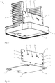
- the figures show an embodiment of a light module 1 according to the invention in various views and in different steps of the assembly of the individual parts.
- the light module 1 comprises a first printed circuit board 10 and a second printed circuit board 20, wherein a plurality of light sources 21-23 are arranged on the second printed circuit board 20.
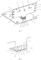
- the first circuit board 10 and the second circuit board 20 are arranged at an angle 8, which is enclosed by the respective conductor planes of the first and second printed circuit board 10, 20, to each other and electrically conductively connected to each other via at least one spring contact element 30-35.
- a right angle 8 exists between the surfaces of the first printed circuit board 10 and the second printed circuit board 20, on each of which strip conductors can be arranged.
- the angle 8 can also assume other values, for example between 45 ° and 135 °, or between 80 ° and 100 °, or between 85 ° and 95 °.
- the spring contact elements 30-35 each have a spring 40 mounted in a holder 50 pin.
- the pin 40 has a cylindrical shape and the end face of the pin 40 is smooth.
- a special shape of the pin of the spring contact element may be favorable, such as a flat, plate or cylindrical end of the pin, a pointed, arrow-like end or a round, spherical end with a smooth or roughened surface. It is possible as a spring contact element and a spring-mounted ball. In this context, it may additionally be advantageous if in addition an elastic or fluid contact agent is applied to the contact surfaces, which is electrically conductive and is adapted to increase the cross-section of the electrical connection formed when contacting a spring contact element with a contact surface to higher To be able to conduct currents via the electrical connection.
- a spring contact element can also be simple and have no holder for a pin.
- the spring contact element may also be a wire which is made of spring steel, is gold-plated for increasing the electrical conductivity, and itself springs. It is advantageous if the spring contact element is SMT-solderable to be suitable for automatic assembly of the board.
- the first circuit board 10 has a plurality of contact surfaces 11-16, which are provided for supporting the pins 40 of the spring contact elements 30-35.
- the holder 50 of the spring contact elements 30-35 is arranged on the second circuit board 20.
- the contact surfaces 11-16 are formed on an outer conductor plane of the first printed circuit board 10, for example in each case by a metal surface produced on the first printed circuit board 10 by structuring a printed circuit board material.
- the contact surfaces may be formed on an end face of the second printed circuit board, for example, in each case by a, applied by electroplating metal coating on the second printed circuit board. This variant is not shown in the figures.
- the first circuit board 10 includes a driver circuit for driving the light sources 21-23, which is not shown in the figures for clarity.
- the driver circuit is connected to the pads 11-16.
- the first circuit board 10 is made of FR4 material, for example.
- the second circuit board 20 is made of IMS material for better heat dissipation of the light sources 21-23.
- the light module 1 is shown, wherein the first circuit board 10 and the second circuit board 20 in a housing 5, which also includes a heat sink 7, are installed.
- the heat sink 7 is connected to the second circuit board 20.
- heat can also be absorbed by the heat sink 7, which heat is emitted from the first circuit board 10 to the connected housing 5 and is emitted via the heat sink 7.
- the light sources 21-23 can be seen on the second printed circuit board 20.
- Fig. 2 shows an arrangement with the first and second circuit boards 10, 20 without the housing.
- the first circuit board 10 has mounting holes 60-63.
- the light sources 21-23 can be seen on the second circuit board 20, which also has mounting holes 70-76.
- FIG. 3 is again the previous arrangement with two printed circuit boards 10, 20 of the light module 1, which are interconnected via spring contact elements 30-35 shown.
- a detail view in the Fig. 4 shows an enlarged section with the spring contact elements 30-35, which each include the holder 50 and the spring-mounted pin 40. The pin 40 rests on a contact surface 11.
- FIG. 5 the first and second printed circuit board 10, 20 of the headlamp 1 are illustrated, the illustration simplifying the first and second printed circuit boards 10, 20 in FIG the final orientation is normal to each other, however, the first and second circuit boards 10, 20 are not connected to each other. As a result, the assignment of the spring contact elements 30-35, or of the respective pin 40 to the contact surfaces 11-16 should be illustrated.
- conductor tracks 17 are shown, which are intended to indicate the electrical connection to a driver circuit.
- the driver circuit is not shown for ease of illustration, but is included in the first circuit board 10.
- Fig. 6 shows the light module 1 with the housing 5, which has a window 6 between the space for the first circuit board 10 and the space for the second circuit board 20.
- an electromagnetic shield with a window 6 is arranged between the first printed circuit board 10 and the second printed circuit board 20.
- the electromagnetic shielding is thus formed by at least part of the housing 5 of the light module 1.
- the housing has 5 mounting devices 81-86, wherein the mounting devices 82 and 85 are each designed as centering pins.
- Fig. 6 shows the light module 1 in a first state in which the first and second circuit boards 10, 20 are not yet inserted into the housing.
- Fig. 7 shows the light module 1 in a second state in which the second circuit board 20 is inserted into the housing 5.
- the centering pins 82, 85 are arranged to cooperate with corresponding openings 72 and 75 on the second circuit board 20.
- Fig. 8 shows the light module 1 in a third state, in which the first circuit board 10 is inserted into the housing 5.
- the spring contact elements 30-35 electrically connect the first and second printed circuit boards 10, 20.
- the light sources 21-23 are in the Fig. 6-8 not shown.
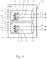
- Fig. 9 schematically shows a motor vehicle headlamp 100 according to the invention with two light modules 1 and 2.
- the light modules 1 and 2 are designed identical in terms of the circuit board assembly, that is, they each have first and second circuit boards 10 and 20 with respective light sources.
- downstream optical elements in the form of optical lenses 110-115 can be designed differently and can thus form different light distributions of a light emitted by the light sources.
- the headlight 100 has a headlight housing 101 in which the two light modules 1, 2 are housed in respective light module housings 102, 103.
- An optically transparent cover 104 is configured to transmit and emit light emitted from the light sources in the form of light beams 121-124.
- the piggyback 100 mounted in a vehicle is configured to illuminate a lane in front of the vehicle.
Landscapes
- Engineering & Computer Science (AREA)
- General Engineering & Computer Science (AREA)
- Microelectronics & Electronic Packaging (AREA)
- Mechanical Engineering (AREA)
- Physics & Mathematics (AREA)
- Optics & Photonics (AREA)
- Manufacturing & Machinery (AREA)
- Non-Portable Lighting Devices Or Systems Thereof (AREA)
- Arrangement Of Elements, Cooling, Sealing, Or The Like Of Lighting Devices (AREA)
Abstract
Description
- Die Erfindung betrifft ein Lichtmodul, umfassend eine erste Leiterplatte und eine zweite Leiterplatte, wobei auf der zweiten Leiterplatte zumindest eine Lichtquelle angeordnet ist.
- Ferner betrifft die Erfindung einen Fahrzeugscheinwerfer, insbesondere einen KFZ-Scheinwerfer.
- Bei modernen Fahrzeugscheinwerfern, insbesondere KFZ-Scheinwerfern, bzw. Lichtmodulen, insbesondere solchen, die eine variable Lichtverteilung erzeugen können, werden vermehrt sehr lichtstarke Lichtquellen, meist Halbleiterdioden in der Form von Hochstrom-LEDs oder Laserdioden eingesetzt. Die Stromaufnahme von Hochstrom-LEDs kann dabei mehrere Ampere betragen. Um die elektrischen Verluste klein zu halten, sollen die stromführenden Verbindungsleitungen kurz und folglich die relevanten Schaltungsteile geometrisch möglichst nahe aneinander liegen. Jedoch steigt durch die geometrische Nähe die Anfälligkeit für unerwünschte Störungen hinsichtlich elektromagnetischer Überkopplung von ersten Schaltungsteilen, durch welche sehr hohe Ströme fließen, zu zweiten Schaltungsteilen, welche empfindliche Elektronikkomponenten enthalten. Diese Störungen sind unerwünscht und sollen vermieden oder reduziert werden.
- Bislang erfolgt dies häufig durch aufwendige und teure Schirmungen, geschirmte und festverlötete Leitungen und geschirmte Steckverbindungen, welche zudem Nachteile durch einen hohen erforderlichen Bauraum und eine komplizierte und teure Montage aufweisen können.
- Steckverbindungen haben überdies den Nachteil, dass bei der Montage beispielsweise durch Verbinden eines Steckers mit einer zugeordneten Buchse relativ große Kräfte auf die Leiterplatten einwirken können, wenn zwei Leiterplatten normal aufeinander angeordnet sind, was wiederum bei Fahrzeugscheinwerfern bzw. Lichtmodulen häufig erforderlich sein kann.
- Ferner können beispielswiese durch thermische Einwirkung während des Betriebs in einem Fahrzeug unerwünschte mechanische Spannungen zwischen zwei Leiterplatten auftreten, welche über eine unelastische Verbindung, beispielsweise durch eine Steckverbindung, miteinander verbunden sind.
- Die Verwendung freiliegender Leitungen zur Verbindung zweier Leiterplatten ist in einem Lichtmodul häufig ungünstig, da die Leitungen häufig zusätzlich fixiert werden müssen, beispielsweise durch Kabelbinder oder Kabelkanäle, um beispielsweise eine Verbreitung durch Vibrationen des Fahrzeugs verursachte unerwünschte mechanische Lasten auf die Leitungen und Leiterplatten zu reduzieren.
- Es ist Aufgabe der Erfindung die Nachteile im Stand der Technik zu überwinden.
- Die Aufgabe wird durch ein Lichtmodul der eingangs genannten Art, insbesondere für einen KFZ-Scheinwerfer, gelöst, indem die erste Leiterplatte und die zweite Leiterplatte unter einem Winkel, welcher durch die jeweiligen Leiterebenen der ersten und zweiten Leiterplatte eingeschlossen ist, zueinander angeordnet sind und über zumindest ein Federkontakt-Element elektrisch leitend miteinander verbunden sind, und der Winkel zwischen der ersten Leiterplatte und der zweiten Leiterplatte zwischen 45° und 135° liegt, bevorzugt zwischen 80° und 100° liegt, und besonders bevorzugt 90° beträgt.
- Dadurch wird erreicht, dass die erste und zweite Leiterplatte auf eine einfache Weise zuverlässig miteinander verbunden werden. Außerdem können durch ein oder mehrere Federkontakt-Elemente mechanische Montagetoleranzen ausgeglichen werden. Ferner wirkt während der Montage nahezu keine Kraft auf die erstmontierte Leiterplatte ein, da die Montagekraft von dem Federkontakt-Element aufgenommen wird.
- Die Verwendung von Federkontakt-Elementen ist aus deshalb sehr vorteilhaft, da das Federkontakt-Element durch automatisierte Standard-Bestückungsverfahren auf einer Leiterplatte montiert werden kann. Dadurch kann die Anzahl an Bearbeitungsschritten und daher die Montagekosten gesenkt werden.
- Es ist besonders vorteilhaft, dass die zu den Federkontakt-Elementen korrespondierenden Kontaktflächen sehr einfach in Form von metallisierten Flächen auf der Leiterplatte selbst hergestellt werden können und keine gesonderten Bauteile erfordern, welche jeweils eine Gegenseite zu dem Federkontakt-Element bilden würden.
- Die Kombination von Federkontakt-Elementen und korrespondierenden Kontaktflächen erlaubt die Führung hoher Ströme (15 Ampere und mehr) über die hergestellte elektrische Verbindung.
- Derartige Verbindungen sind insbesondere zur Herstellung einer niederohmigen Verbindung, beispielsweise eine Masse-Verbindung oder eine EMV-Verbindung zum Schutz vor elektromagnetischen Störungen geeignet.
- In einer ersten Ausführungsvariante weist die erste Leiterplatte zumindest eine Kontaktfläche auf, welche zur Auflage des zumindest einen Federkontakt-Elements vorgesehen ist. Auf der zweiten Leiterplatte ist das zumindest eine Federkontakt-Element angeordnet.
- In einer zweiten Ausführungsvariante ist auf der ersten Leiterplatte das zumindest eine Federkontakt-Element angeordnet. Die zweite Leiterplatte weist zumindest eine Kontaktfläche auf, welche zur Auflage des zumindest einen Federkontakt-Elements vorgesehen ist.
- Es ist günstig, wenn die zumindest eine Kontaktfläche auf einer außenliegenden Leiterebene oder einer Stirnseite der ersten oder zweiten Leiterplatte ausgebildet ist, insbesondere durch eine durch Strukturierung eines Leiterplattenmaterials hergestellte Metallfläche oder eine, beispielsweise durch Galvanisierung aufgebrachte Metallbeschichtung auf der ersten oder zweiten Leiterplatte.
- In manchen Ausführungsvarianten kann es vorteilhaft sein, wenn auf der zumindest einen Kontaktfläche zusätzlich ein elastisches oder fluides Kontaktmittel aufgebracht ist, welches elektrisch leitfähig ist und eingerichtet ist, bei Kontaktieren des zumindest einen Federkontakt-Elements mit der zumindest einen Kontaktfläche den Querschnitt der gebildeten elektrischen Verbindung zu vergrößern, um höhere Ströme über die elektrischen Verbindung leiten zu können. Dazu kann beispielsweise das elastische Kontaktmittel eine gummiartige Auflagematte sein, oder das fluide Kontaktmittel beispielsweise ein Klebstoff oder auch ein Lot sein, falls es für die Anordnung nicht unbedingt erforderlich ist, dass die Verbindung wieder lösbar ist und das fluide Kontaktmittel daher ausgehärtet oder verlötet werden kann. Mit anderen Worten kann die Spitze des Stifts des zumindest einen Federkontakt-Elements und die zumindest eine Kontaktfläche zusätzlich durch ein Kontaktmittel, das zwischen Stift und Kontaktfläche gelegen ist oder den Stift und die Kontaktfläche gemeinsam umgibt, der Querschnitt der elektrisch leitenden Verbindung vergrößert werden, um den Fluss höherer Ströme über die geschaffene Verbindung zu erlauben.
- Es ist vorteilhaft, wenn die erste Leiterplatte eine Treiberschaltung zur Ansteuerung der zumindest einen Lichtquelle umfasst. Dabei ist die Treiberschaltung mit der zumindest einen Kontaktfläche verbunden. Außerdem kann die erste Leiterplatte aus FR4-Material hergestellt sein.
- Es ist günstig, wenn die zweite Leiterplatte aus IMS-Material hergestellt ist. Für Leiterplatten mit hohen Anforderungen an die Wärmeabführung, wie bei einem Lichtmodul, welches Hochleistungsleuchtdioden oder Laserdioden umfassen kann, werden Basismaterialien mit Metallkernen wie Aluminium oder Kupfer verwendet. Diese Trägermaterialien werden auch als Direct Bonded Copper oder als Insulated metal substrate (IMS) bezeichnet.
- Für einen kompakten Aufbau des Scheinwerfers ist es vorteilhaft, wenn zumindest ein Kühlkörper umfasst ist, welcher mit der zweiten Leiterplatte verbunden ist. Zusätzlich kann auch die erste Leiterplatte mit dem zumindest einen Kühlkörper verbunden sein.
- Eine Weiterentwicklung der Erfindung umfasst ein Gehäuse für das Lichtmodul, welches insbesondere für einen KFZ-Scheinwerfer geeignet ist, wobei zwischen dem Bauraum für die erste Leiterplatte und dem Bauraum für die zweite Leiterplatte eine elektromagnetische Schirmung mit einem Fenster angeordnet ist, durch welches Fenster zumindest ein Teil des zumindest einen Federkontakt-Elements hindurch ragt. Das Fenster ist dabei so ausgeführt, dass der Rand des Fensters möglichst nahe an die Federkontakt-Elemente heranreicht. Es ist vorteilhaft, wenn das Fenster in der Geometrie so bemessen ist, dass eine elektromagnetische Überkopplung von ersten elektrischen Signalen der Treiberschaltung, welche auf der ersten Leiterplatte geführt sind, zu zweiten elektrischen Signalen der Lichtquellen, welche auf der zweiten Leiterplatte geführt sind, und umgekehrt, reduziert wird.
- Es ist vorteilhaft, wenn die elektromagnetische Schirmung durch zumindest ein Teil des Gehäuses des Lichtmoduls gebildet ist.
- Die erfindungsgemäße Aufgabe wird auch durch einen eingangs genannten Fahrzeugscheinwerfer gelöst, welcher zumindest ein erfindungsgemäßes Lichtmodul umfasst. Ein erfindungsgemäßes Lichtmodul weist durch die spezifische Anordnung der Leiterplatten Vorteile insbesondere für die Verwendung in einem Kraftfahrzeugscheinwerfer auf, da dadurch sehr vorteilhafte Freiheitsgrade bei der Konzeption und bei der Konstruktion erreicht werden können.
- Für einen erfindungsgemäßen Kraftfahrzeugscheinwerfer bzw. ein erfindungsgemäßes Lichtmodul sind wichtige Teile beschrieben, wobei klar ist, dass ein Scheinwerfer noch viele andere, nicht erwähnte Teile enthält, die einen sinnvollen Einsatz in einem Kraftfahrzeug, wie insbesondere einem PKW oder Motorrad, ermöglichen. Der Übersichtlichkeit halber wird beispielsweise auf eine Ansteuerungselektronik, weitere optische Elemente wie eine Primär- oder eine Projektionsoptik, mechanische Verstelleinrichtungen beziehungsweise Halterungen und weitere Teile eines Scheinwerfer-Gehäuses nicht näher eingegangen.
- Die Erfindung und weitere Vorteile werden im Folgenden anhand von nicht einschränkenden Ausführungsbeispielen näher beschrieben, die in den beiliegenden Zeichnungen veranschaulicht sind. Die Zeichnungen zeigen in
- Fig. 1
- ein Ausführungsbeispiel eines erfindungsgemäßen Lichtmoduls für ein Lichtmodul, insbesondere für einen KFZ-Scheinwerfer, in einer perspektivischen Ansicht,
- Fig. 2
- zwei Leiterplatten des Lichtmoduls der
Fig. 1 in einer perspektivischen Ansicht von unten, - Fig. 3
- zwei Leiterplatten des Lichtmoduls der
Fig. 1 , welche über ein Federkontakt-Element miteinander verbunden sind, in einer perspektivischen Ansicht von oben, - Fig. 4
- eine Detailansicht auf das Federkontakt-Element der
Fig. 3 in einer perspektivischen Ansicht von oben, - Fig. 5
- das Lichtmodul der
Fig. 1 in einer perspektivischen Ansicht von oben, - Fig. 6
- das Lichtmodul der
Fig. 1 in einem ersten Zustand in einer perspektivischen Ansicht von unten, - Fig. 7
- das Lichtmodul der
Fig. 1 in einem zweiten Zustand in einer perspektivischen Ansicht von unten, - Fig. 8
- das Lichtmodul der
Fig. 1 in einem dritten Zustand in einer perspektivischen Ansicht von unten, - Fig. 9
- einen erfindungsgemäßen Fahrzeugscheinwerfer, insbesondere KFZ-Scheinwerfer, mit zwei Lichtmodulen jeweils gemäß der
Fig. 1 in einer schematischen Ansicht. - Unter Bezugnahme auf die Figuren werden nun Ausführungsbeispiele der Erfindung näher erläutert. Insbesondere sind für die Erfindung in einem Scheinwerfer bzw. Lichtmodul wichtige Teile dargestellt, wobei klar ist, dass ein Scheinwerfer noch viele andere, nicht gezeigte Teile enthält, die einen sinnvollen Einsatz in einem Kraftfahrzeug, wie insbesondere einem PKW oder Motorrad, ermöglichen. Der Übersichtlichkeit halber sind daher beispielsweise Kühlvorrichtungen für Bauteile, Ansteuerungselektronik, weitere optische Elemente wie eine Primär- oder eine Projektionsoptik, mechanische Verstelleinrichtungen beziehungsweise Halterungen und weitere Teile eines Scheinwerfer-Gehäuses nicht gezeigt.
- Die Figuren zeigen ein Ausführungsbeispiel eines erfindungsgemäßen Lichtmoduls 1 in verschiedenen Ansichten und in verschiedenen Schritten des Zusammenbaus der Einzelteile.
- Das Lichtmodul 1 umfasst eine erste Leiterplatte 10 und eine zweite Leiterplatte 20, wobei auf der zweiten Leiterplatte 20 mehrere Lichtquellen 21-23 angeordnet sind.
- Die erste Leiterplatte 10 und die zweite Leiterplatte 20 sind unter einem Winkel 8, welcher durch die jeweiligen Leiterebenen der ersten und zweiten Leiterplatte 10, 20 eingeschlossen ist, zueinander angeordnet und über zumindest ein Federkontakt-Element 30-35 elektrisch leitend miteinander verbunden.
- Zwischen den Oberflächen der ersten Leiterplatte 10 und der zweiten Leiterplatte 20, auf welchen jeweils Leiterbahnen angeordnet werden können, liegt in diesem Beispiel ein rechter Winkel 8 vor. Montagebedingt oder durch eine optische Auslegung eines Scheinwerfers gewünscht, kann der Winkel 8 auch andere Werte annehmen, wie beispielsweise zwischen 45° und 135°, oder zwischen 80° und 100°, oder auch zwischen 85° und 95°.
- Die Federkontakt-Elemente 30-35 weisen jeweils einen in einem Halter 50 federnd gelagerten Stift 40 auf. In dieser Ausführungsvariante weist der Stift 40 eine zylindrische Form auf und die Stirnfläche des Stifts 40 ist glatt ausgeführt.
- Je nach Ausführungsform, welche beispielsweise einen flacheren Winkel zwischen der ersten und der zweiten Leiterplatte vorsehen kann, kann eine spezielle Formgebung des Stifts des Federkontakt-Elements günstig sein, wie beispielsweise ein flaches, teller- oder zylinderförmiges Ende des Stifts, ein spitzes, pfeilartiges Ende oder ein rundes, kugelförmiges Ende mit einer glatten oder einer aufgerauten Oberfläche. Es ist als Federkontakt-Element auch eine federnd gelagerte Kugel möglich. In diesem Zusammenhang kann es zusätzlich vorteilhaft sein, wenn auf den Kontaktflächen zusätzlich ein elastisches oder fluides Kontaktmittel aufgebracht ist, welches elektrisch leitfähig ist und eingerichtet ist, bei Kontaktieren eines Federkontakt-Elements mit einer Kontaktfläche den Querschnitt der gebildeten elektrischen Verbindung zu vergrößern, um höhere Ströme über die elektrische Verbindung leiten zu können.
- Ein Federkontaktelement kann auch einfach aufgebaut sein und keinen Halter für einen Stift aufweisen. Beispielsweise kann das Federkontaktelement auch ein Draht sein, der aus Federstahl gefertigt ist, zur Erhöhung der elektrischen Leitfähigkeit vergoldet ist, und selbst federt. Es ist dabei vorteilhaft, wenn das Federkontaktelement SMT-lötbar ist, um für eine automatische Bestückung der Platine geeignet zu sein.
- In dieser Ausführungsform weist die erste Leiterplatte 10 mehrere Kontaktflächen 11-16 auf, welche zur Auflage der Stifte 40 der Federkontakt-Elemente 30-35 vorgesehen sind. Auf der zweiten Leiterplatte 20 ist der Halter 50 der Federkontakt-Elemente 30-35 angeordnet.
- Die Kontaktflächen 11-16 sind auf einer außenliegenden Leiterebene der ersten Leiterplatte 10 ausgebildet, beispielsweise jeweils durch eine, durch Strukturierung eines Leiterplattenmaterials hergestellte Metallfläche auf der ersten Leiterplatte 10.
- Alternativ dazu kann auf der ersten Leiterplatte der Halter der Federkontakt-Elemente angeordnet sein, und die zweite Leiterplatte jeweils eine Kontaktfläche aufweisen, welche zur Auflage des jeweiligen Stifts der Federkontakt-Elemente vorgesehen ist. In diesem Fall können die Kontaktflächen auf einer Stirnseite der zweiten Leiterplatte ausgebildet sein, beispielsweise jeweils durch eine, durch Galvanisierung aufgebrachte Metallbeschichtung auf der zweiten Leiterplatte. Diese Variante ist in den Figuren nicht gezeigt.
- Die erste Leiterplatte 10 umfasst eine Treiberschaltung zur Ansteuerung der Lichtquellen 21-23, wobei dies in den Figuren zur besseren Übersichtlichkeit nicht eingezeichnet ist. Die Treiberschaltung ist mit den Kontaktflächen 11-16 verbunden.
- Die erste Leiterplatte 10 ist beispielsweise aus FR4-Material hergestellt.
- Die zweite Leiterplatte 20 ist zur besseren Wärmeableitung der Lichtquellen 21-23 aus IMS-Material hergestellt.
- In der
Fig. 1 ist das Lichtmodul 1 dargestellt, wobei die erste Leiterplatte 10 und die zweite Leiterplatte 20 in einem Gehäuse 5, welches auch einen Kühlkörper 7 umfasst, eingebaut sind. Der Kühlkörper 7 ist mit der zweiten Leiterplatte 20 verbunden. - Zusätzlich kann vom Kühlkörper 7 auch Wärme aufgenommen werden, welche von der ersten Leiterplatte 10 an das verbundene Gehäuse 5 abgegeben wird und über den Kühlkörper 7 abgegeben wird.
- Die Lichtquellen 21-23 sind auf der zweiten Leiterplatte 20 erkennbar.
-
Fig. 2 zeigt eine Anordnung mit der ersten und zweiten Leiterplatte 10, 20 ohne das Gehäuse. - Die erste Leiterplatte 10 weist Montageöffnungen 60-63 auf.
- Die Lichtquellen 21-23 sind auf der zweiten Leiterplatte 20 erkennbar, welche außerdem Montageöffnungen 70-76 aufweist.
- In der
Fig. 3 ist wiederum die vorhergehende Anordnung mit zwei Leiterplatten 10, 20 des Lichtmoduls 1, welche über Federkontakt-Elemente 30-35 miteinander verbunden sind gezeigt. Eine Detailansicht in derFig. 4 zeigt einen vergrößerten Ausschnitt mit den Federkontakt-Elementen 30-35, welche jeweils den Halter 50 sowie den federnd gelagerten Stift 40 umfassen. Der Stift 40 liegt auf einer Kontaktfläche 11 auf. - In der nachfolgenden
Fig. 5 sind die erste und zweite Leiterplatte 10,20 des Scheinwerfers 1 veranschaulicht, wobei die Darstellung vereinfacht die erste und zweite Leiterplatte 10, 20 in der endgültigen Orientierung normal zueinander zeigt, jedoch die erste und zweite Leiterplatte 10, 20 nicht miteinander verbunden sind. Dadurch soll die Zuordnung der Federkontakt-Elemente 30-35, bzw. des jeweiligen Stifts 40 zu den Kontaktflächen 11-16 illustriert werden. - Außerdem sind Leiterbahnen 17 eingezeichnet, welche die elektrische Verbindung zu einer Treiberschaltung andeuten sollen. Die Treiberschaltung ist zur vereinfachten Darstellung nicht eingezeichnet, ist aber von der ersten Leiterplatte 10 umfasst.
-
Fig. 6 zeigt das Lichtmodul 1 mit dem Gehäuse 5, welches zwischen dem Bauraum für die erste Leiterplatte 10 und dem Bauraum für die zweite Leiterplatte 20 ein Fenster 6 aufweist. Mit anderen Worten ist zwischen der ersten Leiterplatte 10 und der zweiten Leiterplatte 20 eine elektromagnetische Schirmung mit einem Fenster 6 angeordnet. Die elektromagnetische Schirmung ist somit durch zumindest einen Teil des Gehäuses 5 des Lichtmoduls 1 gebildet. - Zusätzlich weist das Gehäuse 5 Montagevorrichtungen 81-86 auf, wobei die Montagevorrichtungen 82 und 85 jeweils als Zentrierstifte ausgeführt sind.
-
Fig. 6 zeigt das Lichtmodul 1 in einem ersten Zustand, bei welchem die erste und zweite Leiterplatte 10, 20 noch nicht in das Gehäuse eingesetzt sind. -
Fig. 7 zeigt das Lichtmodul 1 in einem zweiten Zustand, bei welchem die zweite Leiterplatte 20 in das Gehäuse 5 eingesetzt ist. - Die Zentrierstifte 82, 85 sind eingerichtet, mit korrespondierenden Öffnungen 72 und 75 auf der zweiten Leiterplatte 20 zusammenzuwirken.
- Durch das Fenster 6 ragt zumindest ein Teil der Federkontakt-Elemente 30-35 hindurch.
-
Fig. 8 zeigt das Lichtmodul 1 in einem dritten Zustand, bei welchem auch die erste Leiterplatte 10 in das Gehäuse 5 eingesetzt ist. Die Federkontakt-Elemente 30-35 verbinden die erste und zweite Leiterplatte 10,20 elektrisch leitend. - Der Einfachheit halber sind die Lichtquellen 21-23 in den
Fig. 6-8 nicht eingezeichnet. -
Fig. 9 zeigt schematisch einen erfindungsgemäßen KFZ-Scheinwerfer 100 mit zwei Lichtmodulen 1 und 2. Die Lichtmodule 1 und 2 sind hinsichtlich der Leiterplattenanordnung baugleich ausgeführt, das heißt, sie weisen jeweils erste und zweite Leiterplatten 10 und 20 mit jeweiligen Lichtquellen auf. Je nach Anforderung an den Scheinwerfer 100 können beispielsweise nachgelagerte Optikelemente in Form von optischen Linsen 110-115 unterschiedlich ausgelegt sein und können somit unterschiedliche Lichtverteilungen eines von den Lichtquellen emittierten Lichts formen. - Der Scheinwerfer 100 weist ein Scheinwerfergehäuse 101 auf, in welchem die beiden Lichtmodule 1, 2 in jeweiligen Lichtmodulgehäusen 102,103 untergebracht sind.
- Eine optisch transparente Abdeckung 104 ist dazu eingerichtet, von den Lichtquellen emittiertes Licht in Form von Lichtstrahlen 121-124 durchzulassen und abzustrahlen. Der in einem Fahrzeug entsprechend montierte Schweinwerfer 100 ist dazu eingerichtet, eine vor dem Fahrzeug gelegene Fahrbahn auszuleuchten.
-
- 1, 2
- Lichtmodul
- 5
- Gehäuse
- 6
- Fenster
- 7
- Kühlkörper
- 8
- Winkel
- 10, 20
- Leiterplatte
- 11-16
- Kontaktfläche
- 17
- Leiterbahn
- 21-23
- Lichtquelle
- 30-35
- Federkontakt-Element
- 40
- Stift eines Federkontakt-Elements
- 50
- Halter eines Federkontakt-Elements
- 60-63, 71-76
- Montageöffnung
- 81-86
- Montagevorrichtungen
- 100
- Fahrzeugscheinwerfer
- 101
- Scheinwerfergehäuse
- 102, 103
- Lichtmodulgehäuse
- 104
- transparente Abdeckung
- 110-115
- Optikelement, Linse
- 121-124
- emittiertes Licht, Lichtstrahl
Claims (11)
- Lichtmodul (1, 2), umfassend eine erste Leiterplatte (10) und eine zweite Leiterplatte (20), wobei auf der zweiten Leiterplatte (20) zumindest eine Lichtquelle (21-23) angeordnet ist, dadurch gekennzeichnet, dass
die erste Leiterplatte (10) und die zweite Leiterplatte (20) unter einem Winkel (8), welcher durch die jeweiligen Leiterebenen der ersten und zweiten Leiterplatte (10,20) eingeschlossen ist, zueinander angeordnet sind und über zumindest ein Federkontakt-Element (30-35) elektrisch leitend miteinander verbunden sind, und
der Winkel (8) zwischen der ersten Leiterplatte (10) und der zweiten Leiterplatte (20) zwischen 45° und 135° liegt, bevorzugt zwischen 80° und 100° liegt, besonders bevorzugt 90° beträgt. - Lichtmodul (1, 2) nach Anspruch 1, dadurch gekennzeichnet, dass die erste Leiterplatte (10) zumindest eine Kontaktfläche (11-16) aufweist, welche zur Auflage des zumindest einen Federkontakt-Elements (30-35) vorgesehen ist, und auf der zweiten Leiterplatte (20) das zumindest eine Federkontakt-Element (30-35) angeordnet ist.
- Lichtmodul (1, 2) nach Anspruch 1, dadurch gekennzeichnet, dass auf der ersten Leiterplatte (10) das zumindest eine Federkontakt-Element (30-35) angeordnet ist, und die zweite Leiterplatte (20) zumindest eine Kontaktfläche (11-16) aufweist, welche zur Auflage des zumindest einen Federkontakt-Elements (30-35) vorgesehen ist.
- Lichtmodul (1, 2) nach einem der Ansprüche 2 oder 3, dadurch gekennzeichnet, dass die zumindest eine Kontaktfläche (11-16) auf einer außenliegenden Leiterebene oder einer Stirnseite der ersten oder zweiten Leiterplatte (10, 20) ausgebildet ist, insbesondere durch eine durch Strukturierung eines Leiterplattenmaterials hergestellte Metallfläche oder eine, beispielsweise durch Galvanisierung aufgebrachte Metallbeschichtung auf der ersten oder zweiten Leiterplatte (10, 20).
- Lichtmodul (1, 2) nach einem der vorhergehenden Ansprüche, dadurch gekennzeichnet, dass auf der zumindest einen Kontaktfläche (11-16) zusätzlich ein elastisches oder fluides Kontaktmittel aufgebracht ist, welches elektrisch leitfähig ist und eingerichtet ist, bei Kontaktieren des zumindest einen Federkontakt-Elements (30-35) mit der zumindest einen Kontaktfläche (11-16) den Querschnitt der gebildeten elektrischen Verbindung zu vergrößern.
- Lichtmodul (1, 2) nach einem der vorhergehenden Ansprüche, dadurch gekennzeichnet, dass die erste Leiterplatte (10) eine Treiberschaltung zur Ansteuerung der zumindest einen Lichtquelle (21-23) umfasst, welche Treiberschaltung mit der zumindest einen Kontaktfläche (11-16) verbunden ist, und die erste Leiterplatte (10) vorzugsweise aus FR4-Material hergestellt ist.
- Lichtmodul (1, 2) nach einem der vorhergehenden Ansprüche, dadurch gekennzeichnet, dass die zweite Leiterplatte (20) aus IMS-Material hergestellt ist.
- Lichtmodul (1, 2) nach einem der vorhergehenden Ansprüche, umfassend zumindest einen Kühlkörper (7), dadurch gekennzeichnet, dass der zumindest eine Kühlkörper (7) mit der zweiten Leiterplatte (20) verbunden ist, und vorzugsweise die erste Leiterplatte (10) auch mit dem zumindest einen Kühlkörper (7) verbunden ist.
- Lichtmodul (1, 2) nach einem der vorhergehenden Ansprüche, umfassend ein Gehäuse (5) für das Lichtmodul (1, 2), dadurch gekennzeichnet, dass zwischen der ersten Leiterplatte (10) und der zweiten Leiterplatte (20) eine elektromagnetische Schirmung mit einem Fenster (6) angeordnet ist, durch welches Fenster (6) zumindest ein Teil des zumindest einen Federkontakt-Elements (30-35) hindurch ragt.
- Lichtmodul (1, 2) nach Anspruch 10, dadurch gekennzeichnet, dass die elektromagnetische Schirmung durch zumindest ein Teil des Gehäuses (5) des Lichtmoduls (1, 2) gebildet ist.
- Fahrzeugscheinwerfer (100), umfassend zumindest ein Lichtmodul (1, 2) nach einem der vorhergehenden Ansprüche.
Priority Applications (5)
| Application Number | Priority Date | Filing Date | Title |
|---|---|---|---|
| EP17204004.0A EP3489082B1 (de) | 2017-11-28 | 2017-11-28 | Lichtmodul und fahrzeugscheinwerfer |
| PCT/EP2018/077729 WO2019105639A1 (de) | 2017-11-28 | 2018-10-11 | Lichtmodul und fahrzeugscheinwerfer |
| KR1020207016893A KR20200089288A (ko) | 2017-11-28 | 2018-10-11 | 광 모듈 및 차량 헤드램프 |
| CN201880076672.7A CN111372815B (zh) | 2017-11-28 | 2018-10-11 | 照明模块和车辆头灯 |
| KR2020217000080U KR20210002770U (ko) | 2017-11-28 | 2018-10-11 | 광 모듈 및 차량 헤드램프 |
Applications Claiming Priority (1)
| Application Number | Priority Date | Filing Date | Title |
|---|---|---|---|
| EP17204004.0A EP3489082B1 (de) | 2017-11-28 | 2017-11-28 | Lichtmodul und fahrzeugscheinwerfer |
Publications (2)
| Publication Number | Publication Date |
|---|---|
| EP3489082A1 true EP3489082A1 (de) | 2019-05-29 |
| EP3489082B1 EP3489082B1 (de) | 2021-10-06 |
Family
ID=60629418
Family Applications (1)
| Application Number | Title | Priority Date | Filing Date |
|---|---|---|---|
| EP17204004.0A Active EP3489082B1 (de) | 2017-11-28 | 2017-11-28 | Lichtmodul und fahrzeugscheinwerfer |
Country Status (4)
| Country | Link |
|---|---|
| EP (1) | EP3489082B1 (de) |
| KR (2) | KR20210002770U (de) |
| CN (1) | CN111372815B (de) |
| WO (1) | WO2019105639A1 (de) |
Cited By (4)
| Publication number | Priority date | Publication date | Assignee | Title |
|---|---|---|---|---|
| WO2022078556A1 (de) * | 2020-10-13 | 2022-04-21 | Continental Automotive Gmbh | Verfahren zum herstellen einer leiterplatten-stecker-anordnung |
| US11664615B2 (en) * | 2018-08-07 | 2023-05-30 | Tyco Electronics Japan G.K. | Circuit board having terminal, and circuit board assembly |
| GB2616024A (en) * | 2022-02-23 | 2023-08-30 | Arrival Ltd | A hinge and a joining method |
| EP4431795A1 (de) * | 2023-03-14 | 2024-09-18 | Valeo Vision | Leuchtvorrichtung für kraftfahrzeuge mit befestigungsmitteln zum verbinden eines steckverbinders mit einem substrat |
Families Citing this family (2)
| Publication number | Priority date | Publication date | Assignee | Title |
|---|---|---|---|---|
| DE102021131126A1 (de) * | 2021-11-26 | 2023-06-01 | Delo Industrie Klebstoffe Gmbh & Co. Kgaa | Leuchtenbaugruppe und Verfahren zur Herstellung einer Leuchtenbaugruppe |
| WO2024053591A1 (ja) * | 2022-09-07 | 2024-03-14 | 株式会社小糸製作所 | 車両用灯具 |
Citations (6)
| Publication number | Priority date | Publication date | Assignee | Title |
|---|---|---|---|---|
| DE29910417U1 (de) * | 1999-06-15 | 1999-08-12 | Sidler GmbH & Co, 72072 Tübingen | Reflektorleuchte |
| US6231219B1 (en) * | 1999-03-03 | 2001-05-15 | Kurt L. Lohss | Dual-purpose glovebox light assembly and cradle therefor |
| WO2006066530A1 (de) * | 2004-12-22 | 2006-06-29 | Patent-Treuhand- Gesellschaft Für Elektrische Glühlampen Mbh | Beleuchtungseinrichtung mit mindestens einer leuchtdiode und fahrzeugscheinwerfer |
| EP2781826A1 (de) * | 2013-03-18 | 2014-09-24 | Valeo Vision | Vorrichtung zur Beleuchtung und/oder Signalisierung für Kraftfahrzeuge |
| US20150229057A1 (en) * | 2014-02-10 | 2015-08-13 | Advanced-Connectek Inc. | Electrical connector with one-piece terminals |
| US20160273751A1 (en) * | 2014-09-30 | 2016-09-22 | General Electric Company | Connector and led lighting device including the connector |
Family Cites Families (1)
| Publication number | Priority date | Publication date | Assignee | Title |
|---|---|---|---|---|
| WO2015144469A1 (en) * | 2014-03-27 | 2015-10-01 | Koninklijke Philips N.V. | Efficient board to board connection |
-
2017
- 2017-11-28 EP EP17204004.0A patent/EP3489082B1/de active Active
-
2018
- 2018-10-11 WO PCT/EP2018/077729 patent/WO2019105639A1/de active Application Filing
- 2018-10-11 KR KR2020217000080U patent/KR20210002770U/ko not_active Application Discontinuation
- 2018-10-11 CN CN201880076672.7A patent/CN111372815B/zh active Active
- 2018-10-11 KR KR1020207016893A patent/KR20200089288A/ko not_active Application Discontinuation
Patent Citations (6)
| Publication number | Priority date | Publication date | Assignee | Title |
|---|---|---|---|---|
| US6231219B1 (en) * | 1999-03-03 | 2001-05-15 | Kurt L. Lohss | Dual-purpose glovebox light assembly and cradle therefor |
| DE29910417U1 (de) * | 1999-06-15 | 1999-08-12 | Sidler GmbH & Co, 72072 Tübingen | Reflektorleuchte |
| WO2006066530A1 (de) * | 2004-12-22 | 2006-06-29 | Patent-Treuhand- Gesellschaft Für Elektrische Glühlampen Mbh | Beleuchtungseinrichtung mit mindestens einer leuchtdiode und fahrzeugscheinwerfer |
| EP2781826A1 (de) * | 2013-03-18 | 2014-09-24 | Valeo Vision | Vorrichtung zur Beleuchtung und/oder Signalisierung für Kraftfahrzeuge |
| US20150229057A1 (en) * | 2014-02-10 | 2015-08-13 | Advanced-Connectek Inc. | Electrical connector with one-piece terminals |
| US20160273751A1 (en) * | 2014-09-30 | 2016-09-22 | General Electric Company | Connector and led lighting device including the connector |
Cited By (4)
| Publication number | Priority date | Publication date | Assignee | Title |
|---|---|---|---|---|
| US11664615B2 (en) * | 2018-08-07 | 2023-05-30 | Tyco Electronics Japan G.K. | Circuit board having terminal, and circuit board assembly |
| WO2022078556A1 (de) * | 2020-10-13 | 2022-04-21 | Continental Automotive Gmbh | Verfahren zum herstellen einer leiterplatten-stecker-anordnung |
| GB2616024A (en) * | 2022-02-23 | 2023-08-30 | Arrival Ltd | A hinge and a joining method |
| EP4431795A1 (de) * | 2023-03-14 | 2024-09-18 | Valeo Vision | Leuchtvorrichtung für kraftfahrzeuge mit befestigungsmitteln zum verbinden eines steckverbinders mit einem substrat |
Also Published As
| Publication number | Publication date |
|---|---|
| KR20200089288A (ko) | 2020-07-24 |
| EP3489082B1 (de) | 2021-10-06 |
| CN111372815B (zh) | 2023-07-04 |
| KR20210002770U (ko) | 2021-12-10 |
| WO2019105639A1 (de) | 2019-06-06 |
| CN111372815A (zh) | 2020-07-03 |
Similar Documents
| Publication | Publication Date | Title |
|---|---|---|
| EP3489082B1 (de) | Lichtmodul und fahrzeugscheinwerfer | |
| DE102008000582A1 (de) | LED-Verbindungsfederbügelbauteil | |
| DE102013225411A1 (de) | Verbinder für eine LED-Modulplatine | |
| DE102018117378A1 (de) | Leistungsversorgung, Lampe, bewegliche Vorrichtung und Verfahren zur Herstellung einer Leistungsversorgung | |
| DE102008040460A1 (de) | In LED-Verbindungseinheit integrierte Verbindungsstückhalterung | |
| DE112018000388T5 (de) | Leistungswandler | |
| DE102008031262A1 (de) | Beleuchtungseinheit für Fahrzeugscheinwerfer und Fahrzeugscheinwerfer | |
| EP2347639A1 (de) | Beleuchtungsvorrichtung mit zwei leiterplatten | |
| WO2015007904A1 (de) | Leuchtvorrichtung mit halbleiterlichtquelle und treiberplatine | |
| DE102012218538A1 (de) | Verfahren zur Herstellung einer Lichterzeugungseinheit | |
| DE102011051153A1 (de) | Elektrische Verbindungsvorrichtung für elektrische Komponenten | |
| DE102014109220A1 (de) | Leiterplattenverbindungselement | |
| EP2938170A1 (de) | Halter für SMD-Leuchtdiode | |
| DE102017105997A1 (de) | Sendeeinrichtung für eine optische Erfassungseinrichtung eines Kraftfahrzeugs mit einem spezifischen Vormontagemodul, optische Erfassungseinrichtung sowie Kraftfahrzeug | |
| DE102014202196B3 (de) | Leiterplatte und Schaltungsanordnung | |
| DE102017204251A1 (de) | Elektronische steuereinheit und verfahren zum herstellen derselben | |
| EP2694874A1 (de) | Vorrichtung zum befestigen und kontaktieren eines leuchtmittels und/oder eines leuchtmoduls, sowie leuchte | |
| AT513328B1 (de) | Beleuchtungsvorrichtung | |
| EP3267501B1 (de) | Bestückung von thermisch hochleitfähigen bauteilen zur wärmespreizung | |
| DE102016101757A1 (de) | Schaltungsmodul mit oberflächenmontierbaren unterlagsblöcken zum anschliessen einer leiterplatte | |
| DE102020100742A1 (de) | Leiterplatte, Lichtmodul, Beleuchtungseinrichtung und Kraftfahrzeug | |
| EP1968365B1 (de) | Leiterplatte mit einem winkelförmigen Stanzgitter bestückt | |
| DE202009018077U1 (de) | Leistungselektronikanordnung | |
| DE102019106562A1 (de) | Leiterplatteneinheit | |
| DE102012211143A1 (de) | Träger für elektrisches bauelement mit wärmeleitkörper |
Legal Events
| Date | Code | Title | Description |
|---|---|---|---|
| PUAI | Public reference made under article 153(3) epc to a published international application that has entered the european phase |
Free format text: ORIGINAL CODE: 0009012 |
|
| STAA | Information on the status of an ep patent application or granted ep patent |
Free format text: STATUS: THE APPLICATION HAS BEEN PUBLISHED |
|
| AK | Designated contracting states |
Kind code of ref document: A1 Designated state(s): AL AT BE BG CH CY CZ DE DK EE ES FI FR GB GR HR HU IE IS IT LI LT LU LV MC MK MT NL NO PL PT RO RS SE SI SK SM TR |
|
| AX | Request for extension of the european patent |
Extension state: BA ME |
|
| STAA | Information on the status of an ep patent application or granted ep patent |
Free format text: STATUS: REQUEST FOR EXAMINATION WAS MADE |
|
| 17P | Request for examination filed |
Effective date: 20191029 |
|
| RBV | Designated contracting states (corrected) |
Designated state(s): AL AT BE BG CH CY CZ DE DK EE ES FI FR GB GR HR HU IE IS IT LI LT LU LV MC MK MT NL NO PL PT RO RS SE SI SK SM TR |
|
| STAA | Information on the status of an ep patent application or granted ep patent |
Free format text: STATUS: EXAMINATION IS IN PROGRESS |
|
| 17Q | First examination report despatched |
Effective date: 20210423 |
|
| GRAP | Despatch of communication of intention to grant a patent |
Free format text: ORIGINAL CODE: EPIDOSNIGR1 |
|
| STAA | Information on the status of an ep patent application or granted ep patent |
Free format text: STATUS: GRANT OF PATENT IS INTENDED |
|
| INTG | Intention to grant announced |
Effective date: 20210716 |
|
| GRAS | Grant fee paid |
Free format text: ORIGINAL CODE: EPIDOSNIGR3 |
|
| GRAA | (expected) grant |
Free format text: ORIGINAL CODE: 0009210 |
|
| STAA | Information on the status of an ep patent application or granted ep patent |
Free format text: STATUS: THE PATENT HAS BEEN GRANTED |
|
| AK | Designated contracting states |
Kind code of ref document: B1 Designated state(s): AL AT BE BG CH CY CZ DE DK EE ES FI FR GB GR HR HU IE IS IT LI LT LU LV MC MK MT NL NO PL PT RO RS SE SI SK SM TR |
|
| REG | Reference to a national code |
Ref country code: GB Ref legal event code: FG4D Free format text: NOT ENGLISH |
|
| REG | Reference to a national code |
Ref country code: CH Ref legal event code: EP Ref country code: AT Ref legal event code: REF Ref document number: 1435946 Country of ref document: AT Kind code of ref document: T Effective date: 20211015 |
|
| REG | Reference to a national code |
Ref country code: DE Ref legal event code: R096 Ref document number: 502017011653 Country of ref document: DE |
|
| REG | Reference to a national code |
Ref country code: IE Ref legal event code: FG4D Free format text: LANGUAGE OF EP DOCUMENT: GERMAN |
|
| REG | Reference to a national code |
Ref country code: LT Ref legal event code: MG9D |
|
| REG | Reference to a national code |
Ref country code: NL Ref legal event code: MP Effective date: 20211006 |
|
| PG25 | Lapsed in a contracting state [announced via postgrant information from national office to epo] |
Ref country code: RS Free format text: LAPSE BECAUSE OF FAILURE TO SUBMIT A TRANSLATION OF THE DESCRIPTION OR TO PAY THE FEE WITHIN THE PRESCRIBED TIME-LIMIT Effective date: 20211006 Ref country code: LT Free format text: LAPSE BECAUSE OF FAILURE TO SUBMIT A TRANSLATION OF THE DESCRIPTION OR TO PAY THE FEE WITHIN THE PRESCRIBED TIME-LIMIT Effective date: 20211006 Ref country code: FI Free format text: LAPSE BECAUSE OF FAILURE TO SUBMIT A TRANSLATION OF THE DESCRIPTION OR TO PAY THE FEE WITHIN THE PRESCRIBED TIME-LIMIT Effective date: 20211006 Ref country code: BG Free format text: LAPSE BECAUSE OF FAILURE TO SUBMIT A TRANSLATION OF THE DESCRIPTION OR TO PAY THE FEE WITHIN THE PRESCRIBED TIME-LIMIT Effective date: 20220106 |
|
| PG25 | Lapsed in a contracting state [announced via postgrant information from national office to epo] |
Ref country code: IS Free format text: LAPSE BECAUSE OF FAILURE TO SUBMIT A TRANSLATION OF THE DESCRIPTION OR TO PAY THE FEE WITHIN THE PRESCRIBED TIME-LIMIT Effective date: 20220206 Ref country code: SE Free format text: LAPSE BECAUSE OF FAILURE TO SUBMIT A TRANSLATION OF THE DESCRIPTION OR TO PAY THE FEE WITHIN THE PRESCRIBED TIME-LIMIT Effective date: 20211006 Ref country code: PT Free format text: LAPSE BECAUSE OF FAILURE TO SUBMIT A TRANSLATION OF THE DESCRIPTION OR TO PAY THE FEE WITHIN THE PRESCRIBED TIME-LIMIT Effective date: 20220207 Ref country code: PL Free format text: LAPSE BECAUSE OF FAILURE TO SUBMIT A TRANSLATION OF THE DESCRIPTION OR TO PAY THE FEE WITHIN THE PRESCRIBED TIME-LIMIT Effective date: 20211006 Ref country code: NO Free format text: LAPSE BECAUSE OF FAILURE TO SUBMIT A TRANSLATION OF THE DESCRIPTION OR TO PAY THE FEE WITHIN THE PRESCRIBED TIME-LIMIT Effective date: 20220106 Ref country code: NL Free format text: LAPSE BECAUSE OF FAILURE TO SUBMIT A TRANSLATION OF THE DESCRIPTION OR TO PAY THE FEE WITHIN THE PRESCRIBED TIME-LIMIT Effective date: 20211006 Ref country code: LV Free format text: LAPSE BECAUSE OF FAILURE TO SUBMIT A TRANSLATION OF THE DESCRIPTION OR TO PAY THE FEE WITHIN THE PRESCRIBED TIME-LIMIT Effective date: 20211006 Ref country code: HR Free format text: LAPSE BECAUSE OF FAILURE TO SUBMIT A TRANSLATION OF THE DESCRIPTION OR TO PAY THE FEE WITHIN THE PRESCRIBED TIME-LIMIT Effective date: 20211006 Ref country code: GR Free format text: LAPSE BECAUSE OF FAILURE TO SUBMIT A TRANSLATION OF THE DESCRIPTION OR TO PAY THE FEE WITHIN THE PRESCRIBED TIME-LIMIT Effective date: 20220107 Ref country code: ES Free format text: LAPSE BECAUSE OF FAILURE TO SUBMIT A TRANSLATION OF THE DESCRIPTION OR TO PAY THE FEE WITHIN THE PRESCRIBED TIME-LIMIT Effective date: 20211006 |
|
| REG | Reference to a national code |
Ref country code: CH Ref legal event code: PL |
|
| REG | Reference to a national code |
Ref country code: DE Ref legal event code: R097 Ref document number: 502017011653 Country of ref document: DE |
|
| PG25 | Lapsed in a contracting state [announced via postgrant information from national office to epo] |
Ref country code: SM Free format text: LAPSE BECAUSE OF FAILURE TO SUBMIT A TRANSLATION OF THE DESCRIPTION OR TO PAY THE FEE WITHIN THE PRESCRIBED TIME-LIMIT Effective date: 20211006 Ref country code: SK Free format text: LAPSE BECAUSE OF FAILURE TO SUBMIT A TRANSLATION OF THE DESCRIPTION OR TO PAY THE FEE WITHIN THE PRESCRIBED TIME-LIMIT Effective date: 20211006 Ref country code: RO Free format text: LAPSE BECAUSE OF FAILURE TO SUBMIT A TRANSLATION OF THE DESCRIPTION OR TO PAY THE FEE WITHIN THE PRESCRIBED TIME-LIMIT Effective date: 20211006 Ref country code: MC Free format text: LAPSE BECAUSE OF FAILURE TO SUBMIT A TRANSLATION OF THE DESCRIPTION OR TO PAY THE FEE WITHIN THE PRESCRIBED TIME-LIMIT Effective date: 20211006 Ref country code: LU Free format text: LAPSE BECAUSE OF NON-PAYMENT OF DUE FEES Effective date: 20211128 Ref country code: EE Free format text: LAPSE BECAUSE OF FAILURE TO SUBMIT A TRANSLATION OF THE DESCRIPTION OR TO PAY THE FEE WITHIN THE PRESCRIBED TIME-LIMIT Effective date: 20211006 Ref country code: DK Free format text: LAPSE BECAUSE OF FAILURE TO SUBMIT A TRANSLATION OF THE DESCRIPTION OR TO PAY THE FEE WITHIN THE PRESCRIBED TIME-LIMIT Effective date: 20211006 Ref country code: CZ Free format text: LAPSE BECAUSE OF FAILURE TO SUBMIT A TRANSLATION OF THE DESCRIPTION OR TO PAY THE FEE WITHIN THE PRESCRIBED TIME-LIMIT Effective date: 20211006 Ref country code: BE Free format text: LAPSE BECAUSE OF NON-PAYMENT OF DUE FEES Effective date: 20211130 |
|
| REG | Reference to a national code |
Ref country code: BE Ref legal event code: MM Effective date: 20211130 |
|
| PLBE | No opposition filed within time limit |
Free format text: ORIGINAL CODE: 0009261 |
|
| STAA | Information on the status of an ep patent application or granted ep patent |
Free format text: STATUS: NO OPPOSITION FILED WITHIN TIME LIMIT |
|
| PG25 | Lapsed in a contracting state [announced via postgrant information from national office to epo] |
Ref country code: LI Free format text: LAPSE BECAUSE OF NON-PAYMENT OF DUE FEES Effective date: 20211130 Ref country code: CH Free format text: LAPSE BECAUSE OF NON-PAYMENT OF DUE FEES Effective date: 20211130 |
|
| 26N | No opposition filed |
Effective date: 20220707 |
|
| GBPC | Gb: european patent ceased through non-payment of renewal fee |
Effective date: 20220106 |
|
| PG25 | Lapsed in a contracting state [announced via postgrant information from national office to epo] |
Ref country code: IE Free format text: LAPSE BECAUSE OF NON-PAYMENT OF DUE FEES Effective date: 20211128 Ref country code: GB Free format text: LAPSE BECAUSE OF NON-PAYMENT OF DUE FEES Effective date: 20220106 Ref country code: AL Free format text: LAPSE BECAUSE OF FAILURE TO SUBMIT A TRANSLATION OF THE DESCRIPTION OR TO PAY THE FEE WITHIN THE PRESCRIBED TIME-LIMIT Effective date: 20211006 |
|
| PG25 | Lapsed in a contracting state [announced via postgrant information from national office to epo] |
Ref country code: SI Free format text: LAPSE BECAUSE OF FAILURE TO SUBMIT A TRANSLATION OF THE DESCRIPTION OR TO PAY THE FEE WITHIN THE PRESCRIBED TIME-LIMIT Effective date: 20211006 |
|
| PG25 | Lapsed in a contracting state [announced via postgrant information from national office to epo] |
Ref country code: IT Free format text: LAPSE BECAUSE OF FAILURE TO SUBMIT A TRANSLATION OF THE DESCRIPTION OR TO PAY THE FEE WITHIN THE PRESCRIBED TIME-LIMIT Effective date: 20211006 |
|
| PG25 | Lapsed in a contracting state [announced via postgrant information from national office to epo] |
Ref country code: CY Free format text: LAPSE BECAUSE OF FAILURE TO SUBMIT A TRANSLATION OF THE DESCRIPTION OR TO PAY THE FEE WITHIN THE PRESCRIBED TIME-LIMIT Effective date: 20211006 |
|
| P01 | Opt-out of the competence of the unified patent court (upc) registered |
Effective date: 20230528 |
|
| PG25 | Lapsed in a contracting state [announced via postgrant information from national office to epo] |
Ref country code: HU Free format text: LAPSE BECAUSE OF FAILURE TO SUBMIT A TRANSLATION OF THE DESCRIPTION OR TO PAY THE FEE WITHIN THE PRESCRIBED TIME-LIMIT; INVALID AB INITIO Effective date: 20171128 |
|
| REG | Reference to a national code |
Ref country code: AT Ref legal event code: MM01 Ref document number: 1435946 Country of ref document: AT Kind code of ref document: T Effective date: 20221128 |
|
| PG25 | Lapsed in a contracting state [announced via postgrant information from national office to epo] |
Ref country code: AT Free format text: LAPSE BECAUSE OF NON-PAYMENT OF DUE FEES Effective date: 20221128 |
|
| PGFP | Annual fee paid to national office [announced via postgrant information from national office to epo] |
Ref country code: FR Payment date: 20231120 Year of fee payment: 7 Ref country code: DE Payment date: 20231121 Year of fee payment: 7 |
|
| PG25 | Lapsed in a contracting state [announced via postgrant information from national office to epo] |
Ref country code: MK Free format text: LAPSE BECAUSE OF FAILURE TO SUBMIT A TRANSLATION OF THE DESCRIPTION OR TO PAY THE FEE WITHIN THE PRESCRIBED TIME-LIMIT Effective date: 20211006 |
|
| PG25 | Lapsed in a contracting state [announced via postgrant information from national office to epo] |
Ref country code: TR Free format text: LAPSE BECAUSE OF FAILURE TO SUBMIT A TRANSLATION OF THE DESCRIPTION OR TO PAY THE FEE WITHIN THE PRESCRIBED TIME-LIMIT Effective date: 20211006 |
|
| PG25 | Lapsed in a contracting state [announced via postgrant information from national office to epo] |
Ref country code: MT Free format text: LAPSE BECAUSE OF FAILURE TO SUBMIT A TRANSLATION OF THE DESCRIPTION OR TO PAY THE FEE WITHIN THE PRESCRIBED TIME-LIMIT Effective date: 20211006 |