EP3487058B1 - Efficient switching for converter circuit - Google Patents
Efficient switching for converter circuit Download PDFInfo
- Publication number
- EP3487058B1 EP3487058B1 EP18206400.6A EP18206400A EP3487058B1 EP 3487058 B1 EP3487058 B1 EP 3487058B1 EP 18206400 A EP18206400 A EP 18206400A EP 3487058 B1 EP3487058 B1 EP 3487058B1
- Authority
- EP
- European Patent Office
- Prior art keywords
- switch
- leg
- switches
- switch leg
- switching
- Prior art date
- Legal status (The legal status is an assumption and is not a legal conclusion. Google has not performed a legal analysis and makes no representation as to the accuracy of the status listed.)
- Active
Links
- 239000003990 capacitor Substances 0.000 claims description 20
- 238000000034 method Methods 0.000 claims description 10
- 230000005669 field effect Effects 0.000 claims description 5
- 229910044991 metal oxide Inorganic materials 0.000 claims description 5
- 150000004706 metal oxides Chemical class 0.000 claims description 5
- 239000004065 semiconductor Substances 0.000 claims description 5
- 230000000737 periodic effect Effects 0.000 claims 12
- 230000000903 blocking effect Effects 0.000 description 25
- 230000002457 bidirectional effect Effects 0.000 description 13
- 238000003860 storage Methods 0.000 description 8
- 238000010586 diagram Methods 0.000 description 7
- 230000008901 benefit Effects 0.000 description 6
- 230000007935 neutral effect Effects 0.000 description 6
- 238000006243 chemical reaction Methods 0.000 description 5
- 238000001914 filtration Methods 0.000 description 3
- JMASRVWKEDWRBT-UHFFFAOYSA-N Gallium nitride Chemical compound [Ga]#N JMASRVWKEDWRBT-UHFFFAOYSA-N 0.000 description 2
- 230000000694 effects Effects 0.000 description 2
- HBMJWWWQQXIZIP-UHFFFAOYSA-N silicon carbide Chemical compound [Si+]#[C-] HBMJWWWQQXIZIP-UHFFFAOYSA-N 0.000 description 2
- 229910010271 silicon carbide Inorganic materials 0.000 description 2
- 229910002601 GaN Inorganic materials 0.000 description 1
- 230000000295 complement effect Effects 0.000 description 1
- 238000010276 construction Methods 0.000 description 1
- 230000001419 dependent effect Effects 0.000 description 1
- 238000009826 distribution Methods 0.000 description 1
- 230000017525 heat dissipation Effects 0.000 description 1
- 238000004519 manufacturing process Methods 0.000 description 1
- 230000000116 mitigating effect Effects 0.000 description 1
- 238000012986 modification Methods 0.000 description 1
- 230000004048 modification Effects 0.000 description 1
- 229910003465 moissanite Inorganic materials 0.000 description 1
- 230000003068 static effect Effects 0.000 description 1
- 230000001360 synchronised effect Effects 0.000 description 1
- 230000001052 transient effect Effects 0.000 description 1
Images


Classifications
-
- H—ELECTRICITY
- H02—GENERATION; CONVERSION OR DISTRIBUTION OF ELECTRIC POWER
- H02M—APPARATUS FOR CONVERSION BETWEEN AC AND AC, BETWEEN AC AND DC, OR BETWEEN DC AND DC, AND FOR USE WITH MAINS OR SIMILAR POWER SUPPLY SYSTEMS; CONVERSION OF DC OR AC INPUT POWER INTO SURGE OUTPUT POWER; CONTROL OR REGULATION THEREOF
- H02M7/00—Conversion of ac power input into dc power output; Conversion of dc power input into ac power output
- H02M7/42—Conversion of dc power input into ac power output without possibility of reversal
- H02M7/44—Conversion of dc power input into ac power output without possibility of reversal by static converters
- H02M7/48—Conversion of dc power input into ac power output without possibility of reversal by static converters using discharge tubes with control electrode or semiconductor devices with control electrode
- H02M7/53—Conversion of dc power input into ac power output without possibility of reversal by static converters using discharge tubes with control electrode or semiconductor devices with control electrode using devices of a triode or transistor type requiring continuous application of a control signal
- H02M7/537—Conversion of dc power input into ac power output without possibility of reversal by static converters using discharge tubes with control electrode or semiconductor devices with control electrode using devices of a triode or transistor type requiring continuous application of a control signal using semiconductor devices only, e.g. single switched pulse inverters
-
- H—ELECTRICITY
- H02—GENERATION; CONVERSION OR DISTRIBUTION OF ELECTRIC POWER
- H02M—APPARATUS FOR CONVERSION BETWEEN AC AND AC, BETWEEN AC AND DC, OR BETWEEN DC AND DC, AND FOR USE WITH MAINS OR SIMILAR POWER SUPPLY SYSTEMS; CONVERSION OF DC OR AC INPUT POWER INTO SURGE OUTPUT POWER; CONTROL OR REGULATION THEREOF
- H02M7/00—Conversion of ac power input into dc power output; Conversion of dc power input into ac power output
- H02M7/42—Conversion of dc power input into ac power output without possibility of reversal
- H02M7/44—Conversion of dc power input into ac power output without possibility of reversal by static converters
- H02M7/48—Conversion of dc power input into ac power output without possibility of reversal by static converters using discharge tubes with control electrode or semiconductor devices with control electrode
- H02M7/483—Converters with outputs that each can have more than two voltages levels
- H02M7/487—Neutral point clamped inverters
-
- H—ELECTRICITY
- H02—GENERATION; CONVERSION OR DISTRIBUTION OF ELECTRIC POWER
- H02M—APPARATUS FOR CONVERSION BETWEEN AC AND AC, BETWEEN AC AND DC, OR BETWEEN DC AND DC, AND FOR USE WITH MAINS OR SIMILAR POWER SUPPLY SYSTEMS; CONVERSION OF DC OR AC INPUT POWER INTO SURGE OUTPUT POWER; CONTROL OR REGULATION THEREOF
- H02M1/00—Details of apparatus for conversion
- H02M1/0048—Circuits or arrangements for reducing losses
- H02M1/0054—Transistor switching losses
-
- H—ELECTRICITY
- H02—GENERATION; CONVERSION OR DISTRIBUTION OF ELECTRIC POWER
- H02M—APPARATUS FOR CONVERSION BETWEEN AC AND AC, BETWEEN AC AND DC, OR BETWEEN DC AND DC, AND FOR USE WITH MAINS OR SIMILAR POWER SUPPLY SYSTEMS; CONVERSION OF DC OR AC INPUT POWER INTO SURGE OUTPUT POWER; CONTROL OR REGULATION THEREOF
- H02M1/00—Details of apparatus for conversion
- H02M1/08—Circuits specially adapted for the generation of control voltages for semiconductor devices incorporated in static converters
-
- Y—GENERAL TAGGING OF NEW TECHNOLOGICAL DEVELOPMENTS; GENERAL TAGGING OF CROSS-SECTIONAL TECHNOLOGIES SPANNING OVER SEVERAL SECTIONS OF THE IPC; TECHNICAL SUBJECTS COVERED BY FORMER USPC CROSS-REFERENCE ART COLLECTIONS [XRACs] AND DIGESTS
- Y02—TECHNOLOGIES OR APPLICATIONS FOR MITIGATION OR ADAPTATION AGAINST CLIMATE CHANGE
- Y02B—CLIMATE CHANGE MITIGATION TECHNOLOGIES RELATED TO BUILDINGS, e.g. HOUSING, HOUSE APPLIANCES OR RELATED END-USER APPLICATIONS
- Y02B70/00—Technologies for an efficient end-user side electric power management and consumption
- Y02B70/10—Technologies improving the efficiency by using switched-mode power supplies [SMPS], i.e. efficient power electronics conversion e.g. power factor correction or reduction of losses in power supplies or efficient standby modes
Definitions
- Power converters may be used for converting direct current (DC) voltage to a different DC voltage or an alternating current (AC) voltage.
- Converter construction may typically make use of power transistors and diodes.
- the power transistors and diodes may be operated as electronic switches.
- Certain converter designs may use "hard" switching, which may give rise to switching losses which, for high values of the switching frequency, may cause a reduction in energy conversion efficiency.
- Hard switching may be characterized by a total commutation voltage drop over the current-carrying switch at a current commutation time.
- the voltage may increase up to the value of the commutation voltage while the current continues flowing, before the voltage drops, that may cause high power loss peaks in the switch. It may therefore be desirable to develop converter topologies and switching methods that enable "soft" switching, which may reduce total switching losses.
- high-power converters may make use of a technique referred to as multi-level conversion.
- Multi-level converter design may reduce the occurrence of simultaneously high values of voltage and current, and hence high-power dissipation values, during the switching process. Additionally, multi-level converter topologies may provide multiple output voltage values, which may reduce the size of associated output filters. It may be desirable to develop converter topologies and efficient switching methodologies to improve the cost and/or efficiency of inverters.
- aspects disclosed herein may include an AC/DC converter (also known as an inverter) circuit and a method for converting direct current (DC) power at the inverter circuit input to an alternating current (AC) power at the inverter circuit output.
- the inverter circuit may include circuitry that may be configured to reduce switching and/or conduction losses of switches utilized in the inverter circuit to convert DC power to AC power, and the inverter circuit may provide auxiliary switches to reduce switching losses and to potentially increase efficiency of the inverter circuit.
- a plurality of switches may be connected in series to form a switching leg having an effective voltage blocking capacity equal to about several times the voltage blocking capacity of a single switch.
- the plurality of switches may be configured to dynamically block a first voltage during a first time portion of a switching period, and to statically block a second voltage during a second time portion of a switching period.
- three MOSFETs each having a voltage rating (indicative of a voltage blocking capacity) of Vo volts, for example, 200V, may be connected in series to form an effective switching leg having a voltage rating of about 600V.
- one or more switches of a switching leg may be held in the ON state during a portion of a switching cycle when the voltage applied across the switching leg may be blocked by a reduced number of switches.
- a switching leg of a converter may feature two 600V-rated insulated gate bipolar transistors (IGBT).
- IGBTs 600V-rated insulated gate bipolar transistors
- the switching leg may alternate between conducting (where both IGBTs are ON), and dynamically blocking 600V (where one of the IGBTs is kept ON, and one is turned OFF to block up to 600V).
- both IGBTs may be OFF, statically blocking voltages up to 1200V.
- a switching leg may feature three 200V-rated MOSFET switches. During a switching cycle, the switching leg may alternate between the ON state (i.e., all three switches are ON) and the OFF state (where one or more of the three MOSFETs are OFF). If, for a first portion of a switching cycle, when in the OFF state the switching leg blocks no more than 200V, a single switch may be switched between the ON and OFF states, and two switches may be kept in the ON state throughout the first portion of the switching cycle. When the single switch is OFF, the switching leg dynamically blocks a voltage of up to 200V, and when the single switch is ON (along with the two switches kept in the ON state), the switching leg is conducting.
- the switching leg when in the OFF state the switching leg dynamically blocks no more than 400V, two switches may be switched together between the ON and OFF states, and a single switch may be kept in the ON state throughout the switching period.
- the switching leg When the two switches are ON (along with the single switch kept ON) the switching leg is conducting, and when the two switches are OFF, the switching leg dynamically blocks a voltage up to 400V.
- all three switches may be kept in the OFF state, statically blocking up to 600V.
- a switching leg may have one or more switches switched at a low frequency (e.g., a grid frequency such as 50Hz or 60Hz) and one or more switches switched at a high frequency (e.g., 1kHz, 10kHz, 100kHz, 1MHz or higher).
- a low frequency e.g., a grid frequency such as 50Hz or 60Hz
- a high frequency e.g., 1kHz, 10kHz, 100kHz, 1MHz or higher.
- the high frequency is at least an order of magnitude greater than the low frequency.
- a switching leg may include a leg of one or more main switches, connected in parallel with a leg including one or more auxiliary switches connected in series.
- the main switches may have improved conduction characteristics compared to the auxiliary switches.
- one or more of the auxiliary switches may be turned ON at a short time delay before a corresponding main switch, and the one or more of the auxiliary switches may be turned OFF at a short time delay after the corresponding main switch, to provide soft-switching operating conditions for the main switch.
- the auxiliary switches may replace the main switches, and a switching leg may include a single leg of serially connected switches.
- a switching circuit for a converter.
- the switching circuit includes a plurality of switches connected in series to form a switching leg.
- the switching circuit also includes a controller configured to cause the switching leg to alternate between: a) an ON state in which at least one of the plurality of switches comprising the switching leg is maintained in an ON state and at least one of the plurality of switches comprising the switching leg is switched between an ON state and an OFF state during a first portion of each switching cycle of the switching circuit, and b) an OFF state in which each of the plurality of switches comprising the switching leg is maintained in an OFF state during a second portion of each switching cycle of the switching circuit.
- the switching leg comprises first and second switches each having a voltage rating of Vo volts such that the switching leg has a voltage rating of 2*Vo volts, wherein controller controls the switching leg such that the first switch is switched between an ON state and an OFF state and the second switch is maintained in the ON state during a first portion of each switching cycle, and wherein the switching leg blocks no more than Vo volts during the first portion of each switching cycle, so as to result in dynamic blocking of up to a Vo voltage level during the first portion of each switching cycle.
- the controller controls the switching leg such that the first and second switches are switched to be in an OFF state during a second portion of each switching cycle, so as to result in statically blocking of up to a 2*Vo voltage level during the second portion of each switching cycle.
- the controller controls the switching leg such that the first and second switches are switched to be in an OFF state during a second portion of each switching cycle, so as to result in statically blocking of up to a 2*Vo voltage level during the second portion of each switching cycle.
- the switching leg comprises first, second and third switches each having a voltage rating of Vo volts such that the switching leg has a voltage rating of 3*Vo volts, wherein the first and second switches are each switched between an ON state and an OFF state and the third switches is maintained in the ON state during a first portion of each switching cycle, and wherein the switching leg blocks no more than 2*Vo volts during the first portion of each switching cycle, so as to result in statically blocking of up to a 2*Vo voltage level during the second portion of each switching cycle.
- the controller controls the switching leg such that the first, second and third switches are switched to be in an OFF state during a second portion of each switching cycle, so as to result in statically blocking of up to a 3*Vo voltage level during the second portion of each switching cycle.
- Features of the present invention may be applied to power conversion from DC voltage to a different DC voltage or to AC voltage.
- Features may include reducing switching loss by controlling converter switches to combine dynamic (during a 'PWM' mode of operation) and static (during an 'OFF' mode of operation) voltage blocking, and/or the use of auxiliary switches that may have effective switching transient characteristics connected in parallel to main switches.
- the auxiliary switches connected in parallel to the main switches may help to move the switching losses away from main switches to the higher side of the auxiliary switches, while a substantial majority of current may still flow through main switches.
- 'ON' refers to the active use of a switch during the time period such that during the time period, the switch remains substantially closed circuit (i.e., conducting) for the time period.
- 'OFF' refers to active use of a switch during the time period such that during the time period, the switch remains substantially open circuit (i.e., nonconducting, and statically blocking voltage) for the time period.
- PWM pulse width modulation
- the term “PWM” refers to an active use of a switch for a period of time such that the switch is alternately switched from ON to OFF and vice-versa at a high frequency.
- the active use of the switch during the period of time may include the switch being substantially open circuit (and dynamically blocking voltage) and closed circuit (and conducting) repeatedly during the time period, at a high frequency.
- Power system 10a includes multiple wiring configurations 111.
- Each wiring configuration 111 may include one or more power sources (not shown) that may be connected to a respective power device (also not shown).
- Power sources may be AC power sources (e.g., wind turbines) or sources of DC power derived from wind turbines, battery banks, photovoltaic solar panels, rectified alternating current (AC) or gasoline-powered generators, for example.
- Each wiring configuration 111 may include output terminals A and B.
- the outputs on terminals A and B of the wiring configurations 111 may be connected in series to form a series connection of wiring configuration 111 outputs that may be connected to input terminals C and D of a link unit 107.
- Connected to terminals E and F of link unit 107 are multiple storage devices 106.
- Storage devices 106 may be batteries, flywheels and/ or super capacitors, for example.
- a feature of terminals E and F of link unit 107 may be that link unit 107 may be configurable in order to allow storage devices 106 to be charged from wiring configurations 111 and/or system power device 209 and/or discharged into load 104 via system power device 209.
- Input terminals P and Q of system power device 209 may be connected to terminals G and H of link unit 107.
- System power device 209 may be connected to load 104 and/or multiple loads 104.
- System power device 209 may be a DC to AC inverter and load 104 may be an AC utility grid, for example.
- system power device 209 may be DC combiner boxes, and load 104 may be a DC to AC inverter connected to an AC utility grid.
- FIG. 1B illustrates a block diagram of a power system 10b, according to at least one aspect.
- Power system 10b may be similar to power system 10a except with respect to wiring configurations 111.
- each wiring configuration 111 may include output terminals A and B, whereby the outputs on terminals A and B of the wiring configurations 111 may be connected in parallel to form a parallel connection of wiring configuration 111 outputs that may be connected to input terminals C and D of link unit 107.
- a feature of link units 107 may be to include a power device that may convert power bi-directionally.
- a first direction of power conversion by a power device (such as power device 103 described in descriptions that follow) may be when multiple storage devices 106 are sourced with converted power from the power devices.
- Storage devices 106 may receive converted power from the power devices when storage devices 106 are being charged, for example.
- a second direction of power conversion may be when power from storage devices 106 is converted by the power device to be supplied to loads 104 via system power device 209.
- FIG. 2A shows an inverter 20a according to at least one aspect.
- Inverter 20a may be used as system power device 209 of Figs. 1A or 1B when system power device 209 may be or include an inverter.
- Any of switches SC1-SC6 may be implemented by various solid-state switches (e.g., metal oxide semiconductor field effect transistors (MOSFETs), insulated gate bipolar transistors (IGBT), bipolar junction transistors (BJTs), Silicon-Carbide switches (SiCs), Gallium Nitride (GaN) switches, super-junction transistors, etc.).
- MOSFETs metal oxide semiconductor field effect transistors
- IGBT insulated gate bipolar transistors
- BJTs bipolar junction transistors
- SiCs Silicon-Carbide switches
- GaN Gallium Nitride
- Switches SC1 and SC2 may be serially connected, forming a first switch leg 212.
- Switches SC3 and SC4 may be serially connected, forming a second switch leg 210.
- Switches SC5 and SC6 may be serially connected, forming a third switch leg 211.
- the leg In a leg having two or more serially-connected switches, the leg may be 'OFF' if at least one of the serially-connected switches is 'OFF' without conduction through the switch and through a body diode.
- the leg In a leg having two or more serially-connected switches, the leg may be 'ON if all of the serially-connected switches are 'ON', with conduction through the switch and/or through a body diode.
- Inverter 20a may have an input at terminals P and Q that may receive a DC voltage V dc from a source of DC power or from terminals G and H of switch unit 107.
- the source of DC power e.g., terminals G and H of switch unit 107
- V dc floating input voltage
- nodes N and Np may be may be considered to be connected to a neutral connection point that in electrical systems may be connected to earth or ground.
- connection to the neutral connection point in the description of inverters 20 that follow may provide a bipolar output with a peak AC voltage output at node A alternating between substantially plus V dc divided by two ( V dc /2) and substantially minus V dc divided by two (- V dc /2).
- the output at Node A may alternate for example between substantially plus V dc and substantially zero.
- the midpoint voltage may be substantially plus V dc divided by two ( V dc /2), and the output of inverter 20 may be considered to be unipolar.
- a series connection of capacitors C1 and C2 may connect across terminals P and Q.
- Node N may be the middle connection point between capacitors C1 and C2.
- capacitors C1 and C2 may be replaced by other elements having substantially direct current (DC) voltage.
- Node N may connect to the emitter ( e ) of switch SC1. In a bipolar arrangement, node N may connect to the input terminal ( Np ) of filter 22 that is connected to ground or earth, and in a unipolar arrangement, input terminal Np may connect to terminal Q with input terminal Np not connected to ground or earth.
- Switches SC1 and SC2 are illustrated as insulated gate bipolar transistors (IGBTs), and switches SC3, SC4, SC5 and SC6 are shown as n-channel metal oxide semiconductor field effect transistors (MOSFETs). Switches SC1, SC2, SC3, SC4, SC5 and SC6 may also be implemented using p-channel MOSFETs or a different switch type.
- Collector ( c ) of switch SC1 may connect to the collector ( c ) of switch SC2.
- the emitter ( e ) of switch SC2 may connect to node A that may be connected to input terminal D of filter 22.
- the output of filter 22 on terminals J and K may connect to the input of load 104.
- Load 104 may be a utility grid, for example.
- the drain ( d ) of switch SC3 may connect to terminal P and the source (s) of switch SC3 may connect to the drain ( d ) of switch SC4.
- the source of switch SC4 may connect to node A and to the drain ( d ) of switch SC5.
- the source of switch SC5 may connect to the drain ( d ) of switch SC6.
- the source of switch SC6 may connect to node Q.
- Filter 22 is shown in Fig. 2A as a two-port network with an input terminals D and Np and output terminals J and K.
- filter 22 may be implemented as multiple port networks.
- filters 22a, 22b and 22c may have input terminals D and Np and output terminals J and K and may also be implemented as multiple port networks.
- Filter 22a is shown as a series connection of inductor L2 and capacitor C3 that is connected between input terminal D / output terminal J and input terminal Np / output terminal K.
- LPF 22b is shown as inductor L3 connected between input terminal D and output terminal J. Also, LPF 22b is shown having a through connection that connects input terminal Np to output terminal K.
- LPF 22c is shown as inductor L4 connected in series with inductor L5 between input terminal D and output terminal J.
- One end of capacitor C4 connects at the point between the series connection of inductors L4 and L5.
- the other end of capacitor C4 connects to the through connection that connects input terminal Np to output terminal K.
- inductor L5 might not be included, and terminal J may be connected directly to inductor L4 and capacitor C4.
- the filters of Figs. 2B, 2C and 2D may be cascaded and combined together to form other filter implementations for filter 22.
- LPF 22b may be cascaded before filter 22a such that node J of LPF 22b connects to node D of filter 22a.
- the implementation may further include an additional LPF 22b cascaded after filter 22a such that node D of LPF 22b connects to node J of filter 22a.
- switches SC1 and SC2 may be configured to form a bidirectional switch, for example, by each of switches SC1 and SC2 featuring a diode (either integrated with the switch or connected in parallel to the switch), and connected the anodes of the two diodes or connecting the cathodes of the two diodes, as shown in Fig. 2A .
- switches SC3, SC4, SC5, and SC6 may be considered to perform the role of main switches.
- Switches SC3 and SC4 may form a first main leg, and switches SC5 and SC6 may form a second main leg.
- switches SC3, SC4, SC5, and SC6 may be described in terms of performing an auxiliary role to other main switches, according to at least one aspect.
- the DC input voltage ( V dc ) may be converted into an AC voltage of a certain frequency (e.g., 50Hz or 60Hz) by application of control signals applied to the gates ( g ) of switches SC1-SC6.
- the control signals may be provided by a controller configured to operate switches SC1-SC6.
- the controller may be, for example, a digital signal processor (DSP), application-specific integrated circuit (ASIC), microcontroller, analog control device, or other control devices.
- DSP digital signal processor
- ASIC application-specific integrated circuit
- microcontroller analog control device, or other control devices.
- the topology of inverter 20a may provide three discrete voltage levels at the inverter output (node A ) that may be applied to input terminals D and Np of filter 22.
- the three voltage levels may be substantially plus V dc divided by two ( V dc /2), substantially minus V dc divided by two (- V dc /2) and substantially zero (0) volts.
- the three voltage levels may correspond to three operating Switch States of inverter 20a. Further details of the three Switch States are detailed below when voltage V dc may be considered a bipolar input voltage to inverter 20a.
- Switch State 1 corresponds to a substantially positive voltage V dc divided by two ( V dc /2) at node A
- a flow of current from DC-link voltage ( V dc ) may flow through switches SC3 and SB4 (switches SC3 and SC4 are ON' for a time period while switches SC1, SC2, SC5 and SC6 may be 'OFF' for the time period.
- switches SC5 and SC6 are rated to block the full DC-link voltage
- one of switch SC5 or switch SC6 may be 'ON', with a switching leg comprising switches SC5 and SC6 effectively 'OFF' by virtue of the other one of switches SC5 and SC6 being 'OFF'.
- Switches SC3, SC4, SC5 and SC6 may be 'OFF' and a first current flow from DC-link voltage ( V dc ) through the body diode of switch SC1, through switch SC2 ('PWM' applied) to node A or a second current flow in the opposite direction of the first current through the body diode of switch SC2 and through switch SC1.
- switches SC1 and SC2 may be MOSFETs, both switches SC1 and SC2 may be 'ON' and conduction via a body diode might not be utilized.
- Switch State 3 corresponding to negative V dc divided by two (- V dc /2) at node A, a current flow may be through switches SC5 and SC6 (switches SC5 and SC6 may be 'ON') for a time period while switches SC1, SC2, SC3 and SC4 are 'OFF' for the time period.
- Current may flows through switches SC5 and through switch SC6 that are from node D and through node N (neutral) which may be connected to terminal Np (neutral).
- one of switch SC3 or switch SC4 may be 'ON' with a switching leg comprising switches SC3 and SC4 effectively 'OFF' by virtue of the other one of switches SC3 and SC4 being 'OFF'.
- Switch States 1 and 2 may be alternated at a high frequency (e.g., 5kHz, 10kHz, 16kHz, 100kHz, 200kHz, 1MHz or higher) during a first part of a switching cycle, and Switch States 2 and 3 may be alternated at a high frequency during a second part of a switching cycle.
- switching legs 210 and 212 may be operated in 'PWM' mode (i.e., each of switching legs 210 and 212 alternate between conducting and dynamically blocking the voltage across capacitor C1 ), and switching leg 211 may be operated in 'OFF' mode, i.e., statically blocking the combined voltage across capacitors C1 and C2.
- switching legs 211 and 212 may be operated in 'PWM' mode (i.e., each of switching legs 211 and 212 alternate between conducting and dynamically blocking the voltage across capacitor C2 ), and switching leg 210 may be operated in 'OFF' mode, i.e., statically blocking the combined voltage across capacitors C1 and C2.
- 'PWM' mode i.e., each of switching legs 211 and 212 alternate between conducting and dynamically blocking the voltage across capacitor C2
- switching leg 210 may be operated in 'OFF' mode, i.e., statically blocking the combined voltage across capacitors C1 and C2.
- 'PWM' mode i.e., each of switching legs 211 and 212 alternate between conducting and dynamically blocking the voltage across capacitor C2
- switching leg 210 may be operated in 'OFF' mode, i.e., statically blocking the combined voltage across capacitors C1 and C2.
- Table 1 shows a possible switching table for switches SC1, SC2, SC3 SC4, SC5 and SC6.
- Table 1 Switch State Node A Voltage Level SC1 SC2 SC3 SC4 SC5 SC6 1 +V dc /2 'OFF' 'OFF' ON 'ON' 'OFF'/'ON' 'OFF' 2 0 'ON' ON' 'OFF/'ON" 'OFF' 'OFF' 'OFF' 3 -V dc /2 'OFF' 'OFF' 'OFF' 'OFF' 'ON' 'ON' 'ON' 'ON' 'ON' 'ON'
- Switch State 1 if SC5 is 'OFF', then SC6 is either 'OFF' or 'ON' while maintaining the switching leg including switches SC5 and SC6 in the 'OFF' state.
- Switch State 3 current flows through switch SC6 ('PWM' applied) for a time period while switch SC5 stays substantially closed or 'ON' for the time period.
- the roles are alteranted (e.g., to reduce wear on a particular switch) wherein during a first low-frequency half cycle, switch SC3 is operated in PWM mode and switch SC4 is 'ON' for the time period, and wherein during the next, second, low-frequency half cycle, the roles are reversed where SC4 is-operated in PWM mode and switch SC3 is 'ON' for the time period.
- the three Switch States may present the three discrete voltage levels ( +V dc /2 ,0v and -V dc /2) provided at node A.
- the result of the filtering of the AC voltage at node A applied to the input of filter 22 appears on the output of filter 22 on terminals J and K.
- filter 22 may reduce the amplitudes of the high frequency components of the voltage at node A to achieve an AC voltage on terminals J and K, which is more like a sine wave similar to that provided on a utility grid, for example.
- inverter 20a may be replaced by a DC/DC converter having ode Np connected to terminal Q.
- the voltage output between terminals D and Np is a DC voltage
- load 104 may be a DC load (e.g., a battery or a different type of DC load).
- switching leg 212 may feature only a single switch ( SC2 ), as bidirectional active switching of switching leg 212 might not be necessary.
- Fig. 2E shows waveforms associated with an operating inverter 20a, according to at least one aspect.
- Power inverters may be utilized to produce alternating current (AC) waveforms from direct current (DC) sources such as wiring configurations 111 or different interconnections of wiring configurations 111 and/or storage devices 106 as described above with respect to Figs. 1A and 1B .
- the AC waveforms are derived by filtering voltages produced at node A with the use of filter 22.
- Filtering voltages produced at node A may be required as a result of the effects of the application of control signals to the gates ( g ) of switches SC1-SC6 during operation of switches SC1-SC6 in each of the three Switch States described above and summarized in Table 1 above.
- Inverter 20a may be controlled by control signals responsive to a reference waveform as shown in Fig. 2E as reference waveform 24, which is a sine wave drawn with dotted line.
- the reference waveform may also be triangular waveform, for example.
- frequency modulation may be used or a control signal that includes a variable pulse width and frequency.
- Reference waveform 24 may therefore also represent the desired AC sine wave output on terminals J and K in terms of desired frequency and peak to peak amplitude of substantially V dc .
- Voltage at node A is generated by operating switches SC1-SC6 to track waveform 24 in Fig. 2E .
- the control signals to control inverter 20a are shown as TR1, TR2, TR3, TR4 and TR5, which correspond respectively to the control signals applied to the gates of switches SC1/SC2, SC3, SC4, SC5 and SC6.
- the control signals applied to the gates of switches SC1/SC2, SC3, SC4, SC5 and SC6 are examples of pulse width modulation applied to the gates of switches SC1/SC2, SC3, SC4, SC5 and SC6 to track waveform 24.
- control signals applied to gates ( g ) of inverter 20a may be the application of pulse width modulation (PWM) signals responsive to the reference AC waveform 24 with respect to filter 22 connected to a utility grid or an independent grid to achieve: desired voltage and current amplitudes, frequency, phase balancing, frequency-based power reduction, reactive power control, inverter reconnection conditions, levels of total harmonic distortion, power factor and output power control required by the utility grid and/or the independent grid.
- PWM pulse width modulation
- Inverter 20a may be a neutral-point clamped (NPC) inverter.
- commutation paths may include an outer commutation path of a first leg comprising switches SC3 and SC4 and an inner commutation path of a bidirectional switch comprised of switches SC1 and SC2.
- the commutation paths may further include an outer commutation path of switches SC5 and SC6.
- the bidirectional switch may allow the flow of current in two directions opposite to each other according to modes described in further detail below.
- the bidirectional nature of the bidirectional switch may be by the use of either SC2 and the body diode of switch SC1 or switch SC1 and the body diode of switch SC2 in order to enable the flow of current in two directions opposite to each other.
- Control signal TR1 may be applied to leg 210.
- leg 210 is 'ON' by virtue of either of switch SC1 being on and the body diode of switch SC2 being conductive or by switch SC2 being on and the body diode of switch SC1 being conductive.
- Control signal TR2 may be applied to switch SC3, where when signal TR2 is 'high', switch SC3 is 'ON', and when TR2 is 'low', switch SC4 is 'OFF'.
- TR2 can be observed to switch between 'high' and 'low' at high frequency, indicating that switch SC3 is being operated in a 'PWM' switch state.
- switch TR2 can be observed to be only 'low', indicating that switch SC3 is being operated in an 'OFF' switch state.
- control signals TR3-TR5 may be applied to switches SC4-SC6, respectively.
- the output voltage VA varies at high frequency between 0V and V dc /2, current I1 is positive, and current I1 flows towards to node D.
- the commutation goes back and forth between leg 210 having switches SC3/SC4 and leg 212 having the bidirectional switch using switch SC2 and the body diode of switch SC1.
- current flows alternately through leg 210 and through leg 212.
- Legs 210 and 212 may each be operated in switch state 'PWM' - when leg 210 is ON, leg 212 is OFF (statically blocking the full voltage of at least V dc ), and vice-versa.
- both switches SC3 and SC4 When leg 210 is ON, both switches SC3 and SC4 are in switch state 'ON', and both switches SC1 and SC2 may be in switch state 'OFF'.
- a first switch e.g., SC4
- the second switch e.g., SC3
- switch state 'OFF' dynamically blocking a voltage of up to at least V dc /2.
- Switches SC3 and SC4 may each be rated to withstand a voltage of at least V dc /2, and switches SC3 and SC4 collectively may withstand a voltage of V dc applied between terminals P and Q.
- both switches SC5 and SC6 may be OFF, and switches SC5 and SC6 may each be rated to withstand a voltage of at least V dc /2, such that when both switches SC5 and SC6 are OFF, leg 211 may withstand a voltage of at least V dc .
- a first switch (e.g. SC5 ) of switches SC5 and SC6 may be in switch state 'ON', and the second switch (e.g. SC6 ) may be in switch state 'OFF'.
- Control signal TR5 may be observed to alternate at high frequency between 'high' and 'low', indicating the switch SC6 is being operating in switch state 'PWM'.
- both switches SC3 and SC4 may be OFF, and switches SC3 and SC4 may each be rated to withstand a voltage of at least V dc /2, such that when both switches SC3 and SC4 are OFF, leg 210 may withstand a voltage of at least V dc .
- current I1 is negative while voltage VA may alternate between 0V and V dc /2.
- Current I1 may commutate back and forth between leg 212 (via switch SC1 /body diode of switch SC2 ) and leg 210 (via the body diodes of switches SC3/SC4 ('OFF'), or by turning switch SC3 and/or SC4 ON.
- control signals TR3 and TR4 may be observed to be either continuously 'high' for a period of time (e.g. 220 or 230 ) or continuously 'low for a period of time, indicating that switches SC4 and SC5 are switched at low frequency (e.g., 50Hz or 60Hz) compared to switches SC3 and SC6 (controlled by control signals TR2 and TR5.
- the illustration of Fig. 2E is illustrative only - while control signals TR5 and TR2 are illustrated as switching about 20 times as fast as control signals TR3 and TR4. In practice, control signals TR5 and TR2 may switch 100, 1000 or even 20,000 times faster than control signals TR3 and TR4.
- two serially-connected switches may have reversed roles at different time periods.
- switch SC3 is ON and switch SC4 is operated in PWM mode (alternately conducting and dynamically blocking a voltage of at least V dc /2)
- switch SC4 is ON and switch SC3 is operated in PWM mode.
- PWM mode alternately conducting and dynamically blocking a voltage of at least V dc /2
- second time period 220 e.g., 20 milliseconds later, corresponding to a frequency of 50Hz
- switch SC4 is ON and switch SC3 is operated in PWM mode.
- heat caused by high-frequency switching may be generated at different locations on a circuit board, and overall heat dissipation may be improved.
- one of the switches in leg 210 may be an IGBT (and not a MOSFET, as illustrated) and one of the switches in leg 211 may be an IGBT (and not a MOSFET, as illustrated).
- An IGBT may provide lower conduction losses when compared to a MOSFET, but may suffer from inferior switching characteristics (e.g., higher switching losses).
- switches SC4 and SC5 using IGBTs switched at a low frequency (as shown by control signals TR3 and TR4 in Fig. 2E ), reduced conduction losses at legs 210 and 211 may be obtained.
- Switches SC3-SC6 in the manner illustrated in Fig. 2E may provide certain benefits. For example, switching losses (and heat generated) may be substantially reduced compared to an operation wherein all four switches are switched at a high frequency. As another potential benefit, each switch of switches SC3-SC6 may be rated to withstand a reduced voltage of only V dc /2.
- FIG. 2F illustrates an inverter 20b according to at least one aspect.
- Inverter 20b is similar to inverter 20a, with switching leg 218 replacing leg 210 of Fig. 2A and switching leg 219 replacing leg 211 of Fig. 2A .
- Switching leg 218 may comprise switch SC3 and switches SC40...SC4n.
- Switch SC3 may be operated similarly to as described with regard to Figs. 2A and 2E .
- Control signal TR2 of Fig. 2E may be applied to switch SC3.
- Switches SC40...SC4n may collectively replace switch SC4 of Fig. 2A .
- switch SC6 may be operated similarly to as described with regard to Figs. 2A and 2E .
- Control signal TR5 of Fig. 2E may be applied to switch SC5.
- Switches SC50...S54n may collectively replace switch SC5 of Fig. 2A .
- Switches SC3 and SC6 may be rated to withstand a voltage of at least V dc /2.
- Switches SC40...SC4n may each be rated to withstand a voltage of at least V dc /2n, where n is the number of switches in the group SC40...SC4n.
- Control signal Tr3 of Fig. 2E may be applied to switches SC40...SC4n.
- Switches SC50...SC5n may each be rated to withstand a voltage of at least V dc /2n, where n is the number of switches in the group SC50...SC5n, and control signal Tr4 of Fig. 2E may be applied to switches SC50...SC5n.
- switches SC40...SC4n may be six switches (e.g., MOSFETs), each rated to withstand about 150V and having a conductance resistance ( R ds,on ) of about 3 m ⁇ , resulting in a total conductance resistance of about 20 m ⁇ . (that may substantially reduce conductance losses across switches SC40...SC4n ).
- switches SC40...SC4n may be six switches (e.g., MOSFETs), each rated to withstand about 150V and having a conductance resistance ( R ds,on ) of about 3 m ⁇ , resulting in a total conductance resistance of about 20 m ⁇ . (that may substantially reduce conductance losses across switches SC40...SC4n ).
- switches SC40...SC4n may be switched when switch SC3 is OFF and/or when leg 212 is ON, reducing the risk of an overvoltage across switches SC40...SC4n.
- switches SC50...SC5n may be switched when switch SC6 is OFF and/or when leg 212 is ON, reducing the risk of an overvoltage across switches SC50...SC5n.
- switches SC40...SC4n may be ninety switches, each rated to withstand 10V, and collectively rated to withstand 900V. Switches SC40...SC4n might not be identical; any combination of voltage ratings summing to the desired total voltage rating may be used, which may provide great flexibility in design and potential cost reduction.
- FIG. 3A , 3B and 3C show an inverter 20c, according to at least one aspect.
- Inverter 20c is the same as inverter 20a except with respect to the connection of voltage V dc across terminals P and Q and use of main switches SC7 and SC8 with auxiliary switches SC3, SC4 and SC5, SC6.
- the connection of voltage V dc is a series connection of DC voltage sources V dc1 and V dc2 , where the connection between voltage sources V dc1 and V dc2 is connected to node N by link 30.
- link 30 may be removed and V dc applied to terminals P and Q according to the description above with respect to Fig. 2A .
- connection between voltage sources V dc1 and V dc2 connected to node N may be when voltage sources V dc1 and V dc2 are provided from a series connection of photovoltaic panels that provide respective voltages V dc1 and V dc2 .
- Switches SC3-SC6 may be MOSFETs, as illustrated, and switches SC7 and SC8 may be different types of switches such as an IGBT, SiC or GaN switch.
- Figs. 3A , 3B and 3C correspond to the three Switch States of operation of inverter 20c to provide a three-level output at node A corresponding to V dc /2, 0v and - V dc /2.
- Inverter 20c may be used as system power device 209 when system power device 209 may be or include an inverter.
- the role of switches SC3, SC4 and switches SC5, SC6 may be in an auxiliary role and may be respectively used to mitigate conduction losses of main switches SC7 and SC8.
- switches SC3, SC4 and switches SC5, SC6 in the description that follows are referred to as auxiliary switches.
- main switches SC7 and SC8 may be implemented as IGBTs
- a possible drawback to IGBTs may be their slower switching speed when compared with the switching speeds of MOSFETs for example.
- Mitigation of switching losses of main switches SC7 and SC8 may be such that on their own, main switches SC7 and SC8 are rated to block the full DC-link voltage Vdc , and may commutate at half the DC link voltage ( ⁇ V dc /2) when operated in 'PWM' mode.
- auxiliary switches SC3, SC4, SC5, and SC6 may be utilized to compensate for possible conduction losses of main switches SC7 and SC8 as well as to compensate for possible increased switching losses of main switches SC7 and SC8 due to increased demand for higher DC link voltages ( V dc ).
- Main switch SC7 may be switched substantially in tandem with one of switches SC3 and SC4. For example, where SC3 is PWM-switched for time period 220 of Fig. 2E , main switch SC7 may be switched substantially at the same time as switch SC4. As will be discussed in greater detail below (see Fig. 4 ), a slight delay may be inserted when switching SC3 and SC7 in tandem, to provide zero-voltage switching conditions for switch SC7. Such a slight delay may correspond to a value between 1 ⁇ sec and 10 ⁇ sec in some aspects.
- Figs. 3A , 3B , 3C include marked areas in grey lines to indicate the commutation paths.
- the commutation paths may include an outer commutation path through leg 215 having main switch SC7 and auxiliary switches SC3/SC4, and an inner commutation path through leg 212 having a bidirectional switch composed of switches SC1 and SC2.
- the commutation paths may further include an outer commutation path through leg 216 having main switch SC8 and auxiliary switches SC5/SC6.
- the bidirectional switch allows the flow of current in two directions opposite to each other according to modes described in further detail below.
- the bidirectional nature of the bidirectional switch may be by the use of either SC2 and the body diode of switch SC1 or switch SC1 and the body diode of switch SC2 in order to enable the flow of current in two directions opposite to each other.
- control signals to control inverter 20c are shown as TR1, TR2, TR3, TR4 and TR5 that correspond respectively to the control signals applied to the gates of switches SC1/SC2, SC7/SC3, SC4, SC5 and SC6/SC8.
- Figs. 3A , 3B , 3C may similarly have similar control signals that correspond with the control signals applied to gates ( g ) of inverter 20a.
- the control signals may be the application of pulse width modulation (PWM) signals responsive to reference AC waveform 24 as shown in Fig. 2E .
- PWM pulse width modulation
- inverter 20c may be controlled to achieve: desired voltage and current amplitudes, frequency, phase balancing, frequency-based power reduction, reactive power control, inverter reconnection conditions, levels of total harmonic distortion, power factor and output power control required by the utility grid and/or load.
- frequency modulation may be used or a control signal that includes a variable pulse width and frequency.
- the commutation paths may include a first outer commutation path through leg 215 having of main switch SC7 /auxiliary switches SC3/SC4 and an inner commutation path through leg 212 having a bidirectional switch composed of switches SC1 and SC2.
- the commutation paths may further include a second outer commutation path through leg 216 having main switch SC8 /auxiliary switches SC5/SC6 and through leg 212 having the bidirectional switch.
- switches SC3, SC4, SC5 and SC6 are used as main switches in inverter 20a.
- switching on of one of the switches is by application of PWM to the one switch for a time period whilst the other switch (e.g., switch SC4) remains 'ON' during the time period.
- switch SC3 Since the two switches are connected in series and operated in Switch State 1 such that switch SC4 is 'ON' before switch SC3 is on and switch SC3 goes 'OFF' before switch SC4 is 'OFF', the voltage across switch SC3 ('PWM' applied) is halved so switching losses are reduced and a possible problem of trying to control both switches SC3 and SC4 both being on may also be eliminated.
- the benefits of lower switching losses and simplified control of the possible problem of trying to control both switches SC3 and SC4 both being 'ON' may then further be added to the additional features of inverter 20c.
- Auxiliary switches SC3, SC4 and SC5, SC6 may be respectively connected in parallel to the main switches SC7 and SC8, which may help to move the switching losses away from main switches SC7 and SC8.
- the switching losses may move to the higher side of auxiliary switches SC3, SC5 while a substantial majority of current may still flow through main switches SC7 and SC8.
- two auxiliary switches may be connected in a series connection and the series connection connected across the main switch. Switching of the main switch may be by application of PWM to the main switch and one of the auxiliary switches for a time period with the other auxiliary switch remaining 'ON' during the time period.
- three auxiliary switches may be wired in series where switching of the main switch is by application of PWM to the main switch and one of the auxiliary switches for a time period with the other two auxiliary switches remaining 'ON' during the time period.
- Power converter 20d may feature a first switching leg 240 including hybrid switching circuit 241 connected in series to serial switching circuit 242.
- Hybrid switching circuit 241 may be arranged in a manner the same as or similar to switches SC3, SC4 and SC7 of Fig. 3A
- serial switching circuit 242 may include a series connection of switches (e.g., MOSFETs), similar to or the same as switches SC40...SC4n of Fig. 2F .
- Power converter 20d may further feature a second switching leg 250 including hybrid switching circuit 251 connected in series to serial switching circuit 252.
- Hybrid switching circuit 251 may be arranged in a manner the same as or similar to switches SC5, SC6 and SC8 of Fig. 3A
- serial switching circuit 252 may include a series connection of switches (e.g., MOSFETs).
- First switching leg 240 may alternate between an OFF mode of operation (e.g., where the switching leg 240 statically blocks the full input DC voltage for about half of a low-frequency time period, e.g., for about 10ms of a 20ms time period corresponding to a 50Hz frequency) and a PWM mode of operation (where the switching leg alternates, at high frequency, between (i) dynamically blocking half of the input DC voltage and (ii) conducting).
- OFF mode of operation all of the switches in switching leg 240 may be OFF.
- serial switching circuit 242 When in the PWM mode of operation, serial switching circuit 242 may be ON, and hybrid switching circuit 241 may alternate (at high frequency) between ON and OFF (dynamically blocking about half of the input DC voltage).
- hybrid switching circuit 241 may utilize a first switch (e.g., an IGBT) as a main switch, and one or more additional switches (e.g. MOSFETs) as auxiliary switching for reducing conduction losses.
- a first switch e.g., an IGBT
- additional switches e.g. MOSFETs
- Second switching leg 250 may be constructed and operated in a similar but complementary manner to first switching leg 240.
- Timing diagram 400 shows gate voltage signals that may be applied to switches SC3, SC4 and SC7 of Fig. 3A .
- Timing diagram 400 shows an auxiliary switch gate signal 401 and a main switch gate signal 402.
- the main switch may be, for example, switch SC7 of Fig. 3A
- the auxiliary switch may be, for example, switch SC3 of Fig. 3A (where switch SC4 may be switched at a low frequency) or switch SC4 of Fig. 3A (where switch SC3 may be switched at a low frequency).
- the main and auxiliary switches may be operated as follows:
- a benefit of wiring two or three auxiliary switches in a series connection across a main switch and/or mains switches connected and operated in series compared to a single main switch and/or single auxiliary switch may be that operating (i.e., blocking) voltage demands for the auxiliary switches may be reduced respectively by a half or a third by virtue of the series connection. Reduced voltages may reduce conduction losses of the switches. Reduction in operating voltage may reduce manufacturing cost of inverters due to overall cost of implementing series connections of main switches and/or auxiliary switches for Switch States 1, 2 and 3 compared to one main switch and/or one auxiliary switch for Switch States 1, 2 and 3, for example.
- switches may be applied to similar three phase inverter circuit implementations also.
- the same use of switches may be applied to other neutral point clamped inverter topologies for both three phase and single phase inverters.
- the same use of switches may also be similarly applied to multi-level inverters of various types.
Description
- This application claims priority to
U.S. provisional application serial number 62/588,474, filed November 20, 2017 - Background information can be found in XP055762565 and
EP2413489A1 ,US2011/193412A1 ,EP2953258A2 ,EP2871765A1 , XP011550305,US2017/302153A1 ,WO2014/082221A1 . Power converters may be used for converting direct current (DC) voltage to a different DC voltage or an alternating current (AC) voltage. Converter construction may typically make use of power transistors and diodes. The power transistors and diodes may be operated as electronic switches. Certain converter designs may use "hard" switching, which may give rise to switching losses which, for high values of the switching frequency, may cause a reduction in energy conversion efficiency. Hard switching may be characterized by a total commutation voltage drop over the current-carrying switch at a current commutation time. In case of hard switching, the voltage may increase up to the value of the commutation voltage while the current continues flowing, before the voltage drops, that may cause high power loss peaks in the switch. It may therefore be desirable to develop converter topologies and switching methods that enable "soft" switching, which may reduce total switching losses. - In attempts to improve converter efficiency and reduce costs, high-power converters may make use of a technique referred to as multi-level conversion. Multi-level converter design may reduce the occurrence of simultaneously high values of voltage and current, and hence high-power dissipation values, during the switching process. Additionally, multi-level converter topologies may provide multiple output voltage values, which may reduce the size of associated output filters. It may be desirable to develop converter topologies and efficient switching methodologies to improve the cost and/or efficiency of inverters.
- The following summary is a short summary of some of the inventive concepts for illustrative purposes only, and is not intended to limit or constrain the inventions and examples in the detailed description. One skilled in the art will recognize other novel combinations and features from the detailed description. The invention is defined by the features of
independent apparatus claim 1 and corresponding independent method claim 12. The dependent claims recite advantageous embodiments of the invention. - Aspects disclosed herein may include an AC/DC converter (also known as an inverter) circuit and a method for converting direct current (DC) power at the inverter circuit input to an alternating current (AC) power at the inverter circuit output. According to at least one aspect, the inverter circuit may include circuitry that may be configured to reduce switching and/or conduction losses of switches utilized in the inverter circuit to convert DC power to AC power, and the inverter circuit may provide auxiliary switches to reduce switching losses and to potentially increase efficiency of the inverter circuit.
- According to at least one aspect, a plurality of switches (e.g., metal oxide semiconductor field effect transistors (MOSFETs)) may be connected in series to form a switching leg having an effective voltage blocking capacity equal to about several times the voltage blocking capacity of a single switch. The plurality of switches may be configured to dynamically block a first voltage during a first time portion of a switching period, and to statically block a second voltage during a second time portion of a switching period. For example, three MOSFETs, each having a voltage rating (indicative of a voltage blocking capacity) of Vo volts, for example, 200V, may be connected in series to form an effective switching leg having a voltage rating of about 600V. To reduce switching loss and/or to reduce a need for highly-synchronized switching, one or more switches of a switching leg may be held in the ON state during a portion of a switching cycle when the voltage applied across the switching leg may be blocked by a reduced number of switches.
- For example, a switching leg of a converter may feature two 600V-rated insulated gate bipolar transistors (IGBT). During a switching cycle, for a first portion of the switching cycle, the switching leg may alternate between conducting (where both IGBTs are ON), and dynamically blocking 600V (where one of the IGBTs is kept ON, and one is turned OFF to block up to 600V). For a second portion of the switching cycle, both IGBTs may be OFF, statically blocking voltages up to 1200V.
- As another example, a switching leg may feature three 200V-rated MOSFET switches. During a switching cycle, the switching leg may alternate between the ON state (i.e., all three switches are ON) and the OFF state (where one or more of the three MOSFETs are OFF). If, for a first portion of a switching cycle, when in the OFF state the switching leg blocks no more than 200V, a single switch may be switched between the ON and OFF states, and two switches may be kept in the ON state throughout the first portion of the switching cycle. When the single switch is OFF, the switching leg dynamically blocks a voltage of up to 200V, and when the single switch is ON (along with the two switches kept in the ON state), the switching leg is conducting. If, for a second portion of the switching cycle, when in the OFF state the switching leg dynamically blocks no more than 400V, two switches may be switched together between the ON and OFF states, and a single switch may be kept in the ON state throughout the switching period. When the two switches are ON (along with the single switch kept ON) the switching leg is conducting, and when the two switches are OFF, the switching leg dynamically blocks a voltage up to 400V. For a third portion of the switching period, when the switching leg is required to block over 400V, all three switches may be kept in the OFF state, statically blocking up to 600V.
- According to at least one aspect, a switching leg may have one or more switches switched at a low frequency (e.g., a grid frequency such as 50Hz or 60Hz) and one or more switches switched at a high frequency (e.g., 1kHz, 10kHz, 100kHz, 1MHz or higher). By way of example and not by way of limitation, the high frequency is at least an order of magnitude greater than the low frequency.
- According to at least one aspect, a switching leg may include a leg of one or more main switches, connected in parallel with a leg including one or more auxiliary switches connected in series. The main switches may have improved conduction characteristics compared to the auxiliary switches. When switching a switching leg, one or more of the auxiliary switches may be turned ON at a short time delay before a corresponding main switch, and the one or more of the auxiliary switches may be turned OFF at a short time delay after the corresponding main switch, to provide soft-switching operating conditions for the main switch.
- According to at least one aspect, the auxiliary switches may replace the main switches, and a switching leg may include a single leg of serially connected switches.
- According to at least one aspect, there is provided a switching circuit for a converter. The switching circuit includes a plurality of switches connected in series to form a switching leg. The switching circuit also includes a controller configured to cause the switching leg to alternate between: a) an ON state in which at least one of the plurality of switches comprising the switching leg is maintained in an ON state and at least one of the plurality of switches comprising the switching leg is switched between an ON state and an OFF state during a first portion of each switching cycle of the switching circuit, and b) an OFF state in which each of the plurality of switches comprising the switching leg is maintained in an OFF state during a second portion of each switching cycle of the switching circuit.
- According to the at least one aspect described above, the switching leg comprises first and second switches each having a voltage rating of Vo volts such that the switching leg has a voltage rating of 2*Vo volts, wherein controller controls the switching leg such that the first switch is switched between an ON state and an OFF state and the second switch is maintained in the ON state during a first portion of each switching cycle, and wherein the switching leg blocks no more than Vo volts during the first portion of each switching cycle, so as to result in dynamic blocking of up to a Vo voltage level during the first portion of each switching cycle.
- According to the at least one aspect described above, the controller controls the switching leg such that the first and second switches are switched to be in an OFF state during a second portion of each switching cycle, so as to result in statically blocking of up to a 2*Vo voltage level during the second portion of each switching cycle.
- According to the at least one aspect described above, the controller controls the switching leg such that the first and second switches are switched to be in an OFF state during a second portion of each switching cycle, so as to result in statically blocking of up to a 2*Vo voltage level during the second portion of each switching cycle.
- According to the at least one aspect described above, the switching leg comprises first, second and third switches each having a voltage rating of Vo volts such that the switching leg has a voltage rating of 3*Vo volts, wherein the first and second switches are each switched between an ON state and an OFF state and the third switches is maintained in the ON state during a first portion of each switching cycle, and wherein the switching leg blocks no more than 2*Vo volts during the first portion of each switching cycle, so as to result in statically blocking of up to a 2*Vo voltage level during the second portion of each switching cycle.
- According to the at least one aspect described above, the controller controls the switching leg such that the first, second and third switches are switched to be in an OFF state during a second portion of each switching cycle, so as to result in statically blocking of up to a 3*Vo voltage level during the second portion of each switching cycle.
- As noted above, this Summary is merely a summary of some of the features described herein. It is not exhaustive, and it is not to be a limitation on the claims.
- These and other features, aspects, and advantages of the present disclosure will become better understood with regard to the following description, claims, and drawings. The present disclosure is illustrated by way of example, and not limited by, the accompanying figures.
-
Figs. 1A and 1B illustrate block diagrams of power systems, according to at least one aspect. -
Fig. 2A shows an inverter implementation, according to at least one aspect. -
Figs. 2B, 2C and 2D show further details of implementations of a filter shown inFig. 2A , according to at least one aspect. -
Fig. 2E shows waveforms of the operation of an inverter, according to at least one aspect. -
Fig. 2F shows an inverter implementation, according to at least one aspect. -
Figs. 3A ,3B ,3C are drawings of an inverter indicating paths of current flow, according to at least one aspect. -
Fig. 3D illustrates a power converter, according to at least one aspect. -
Fig. 4 shows a timing diagram for operating switches, according to at least one aspect. - In the following description of various illustrative aspects, reference is made to the accompanying drawings, which form a part hereof, and in which is shown, by way of illustration, various aspects in which aspects of the disclosure may be practiced. It is to be understood that other aspects may be utilized and structural and functional modifications may be made, without departing from the scope of the present disclosure.
- Features of the present invention may be applied to power conversion from DC voltage to a different DC voltage or to AC voltage. Features may include reducing switching loss by controlling converter switches to combine dynamic (during a 'PWM' mode of operation) and static (during an 'OFF' mode of operation) voltage blocking, and/or the use of auxiliary switches that may have effective switching transient characteristics connected in parallel to main switches. The auxiliary switches connected in parallel to the main switches may help to move the switching losses away from main switches to the higher side of the auxiliary switches, while a substantial majority of current may still flow through main switches.
- The term 'ON' as used herein with respect to the operation of switches described below, refers to the active use of a switch during the time period such that during the time period, the switch remains substantially closed circuit (i.e., conducting) for the time period. The term 'OFF' as used herein is with respect to the operation of switches described below and refers to active use of a switch during the time period such that during the time period, the switch remains substantially open circuit (i.e., nonconducting, and statically blocking voltage) for the time period. The term "PWM" as used herein is with respect to the operation of switches described below. As such, unless otherwise stated, the term "PWM" refers to an active use of a switch for a period of time such that the switch is alternately switched from ON to OFF and vice-versa at a high frequency. The active use of the switch during the period of time may include the switch being substantially open circuit (and dynamically blocking voltage) and closed circuit (and conducting) repeatedly during the time period, at a high frequency.
- The term "multiple" as used here in the detailed description indicates the property of having or involving several parts, elements, or members. The claim term "a plurality of" as used herein in the claims section finds support in the description with use of the term "multiple" and/or other plural forms. Other plural forms may include for example regular nouns that form their plurals by adding either the letter 's' or 'es' so that the plural of converter is converters or the plural of switch is switches for example.
- Reference is now made to
Fig. 1A , which illustrates a block diagram of apower system 10a, according to at least one aspect.Power system 10a includesmultiple wiring configurations 111. Eachwiring configuration 111 may include one or more power sources (not shown) that may be connected to a respective power device (also not shown). Power sources may be AC power sources (e.g., wind turbines) or sources of DC power derived from wind turbines, battery banks, photovoltaic solar panels, rectified alternating current (AC) or gasoline-powered generators, for example. Eachwiring configuration 111 may include output terminals A and B. The outputs on terminals A and B of thewiring configurations 111 may be connected in series to form a series connection ofwiring configuration 111 outputs that may be connected to input terminals C and D of alink unit 107. Connected to terminals E and F oflink unit 107 aremultiple storage devices 106.Storage devices 106 may be batteries, flywheels and/ or super capacitors, for example. A feature of terminals E and F oflink unit 107 may be thatlink unit 107 may be configurable in order to allowstorage devices 106 to be charged from wiringconfigurations 111 and/orsystem power device 209 and/or discharged intoload 104 viasystem power device 209. Input terminals P and Q ofsystem power device 209 may be connected to terminals G and H oflink unit 107. The output terminals J and K ofsystem power device 209 may be connected to load 104 and/ormultiple loads 104.System power device 209 according to one or more aspects may be a DC to AC inverter and load 104 may be an AC utility grid, for example. As another example,system power device 209 may be DC combiner boxes, and load 104 may be a DC to AC inverter connected to an AC utility grid. - Reference is now made to
Fig. 1B , which illustrates a block diagram of apower system 10b, according to at least one aspect.Power system 10b may be similar topower system 10a except with respect towiring configurations 111. Inpower system 10b, eachwiring configuration 111 may include output terminals A and B, whereby the outputs on terminals A and B of thewiring configurations 111 may be connected in parallel to form a parallel connection ofwiring configuration 111 outputs that may be connected to input terminals C and D oflink unit 107. - A feature of
link units 107 according to certain aspects may be to include a power device that may convert power bi-directionally. A first direction of power conversion by a power device (such as power device 103 described in descriptions that follow) may be whenmultiple storage devices 106 are sourced with converted power from the power devices.Storage devices 106 may receive converted power from the power devices whenstorage devices 106 are being charged, for example. A second direction of power conversion may be when power fromstorage devices 106 is converted by the power device to be supplied toloads 104 viasystem power device 209. - Reference is now made to
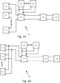
Fig. 2A , which shows aninverter 20a according to at least one aspect.Inverter 20a may be used assystem power device 209 ofFigs. 1A or 1B whensystem power device 209 may be or include an inverter. Any of switches SC1-SC6 may be implemented by various solid-state switches (e.g., metal oxide semiconductor field effect transistors (MOSFETs), insulated gate bipolar transistors (IGBT), bipolar junction transistors (BJTs), Silicon-Carbide switches (SiCs), Gallium Nitride (GaN) switches, super-junction transistors, etc.). - Switches SC1 and SC2 may be serially connected, forming a
first switch leg 212. Switches SC3 and SC4 may be serially connected, forming asecond switch leg 210. Switches SC5 and SC6 may be serially connected, forming athird switch leg 211. In a leg having two or more serially-connected switches, the leg may be 'OFF' if at least one of the serially-connected switches is 'OFF' without conduction through the switch and through a body diode. In a leg having two or more serially-connected switches, the leg may be 'ON if all of the serially-connected switches are 'ON', with conduction through the switch and/or through a body diode. -
Inverter 20a may have an input at terminals P and Q that may receive a DC voltage Vdc from a source of DC power or from terminals G and H ofswitch unit 107. The source of DC power (e.g., terminals G and H of switch unit 107) may be a floating input voltage (Vdc ), or either of terminals G and H may be connected to a ground. In the descriptions that follow, nodes N and Np may be may be considered to be connected to a neutral connection point that in electrical systems may be connected to earth or ground. As such, the connection to the neutral connection point in the description of inverters 20 that follow may provide a bipolar output with a peak AC voltage output at node A alternating between substantially plus Vdc divided by two (Vdc /2) and substantially minus Vdc divided by two (-Vdc /2). Where nodes N and Np might be not connected to the neutral connection point (e.g., where node Q might not be connected to a reference and/or ground point), the output at Node A may alternate for example between substantially plus Vdc and substantially zero. In such a case, the midpoint voltage may be substantially plus Vdc divided by two (Vdc /2), and the output of inverter 20 may be considered to be unipolar. - A series connection of capacitors C1 and C2 may connect across terminals P and Q. Node N may be the middle connection point between capacitors C1 and C2. According to aspects of the disclosure, capacitors C1 and C2 may be replaced by other elements having substantially direct current (DC) voltage. Node N may connect to the emitter (e) of switch SC1. In a bipolar arrangement, node N may connect to the input terminal (Np) of
filter 22 that is connected to ground or earth, and in a unipolar arrangement, input terminal Np may connect to terminal Q with input terminal Np not connected to ground or earth. Switches SC1 and SC2 are illustrated as insulated gate bipolar transistors (IGBTs), and switches SC3, SC4, SC5 and SC6 are shown as n-channel metal oxide semiconductor field effect transistors (MOSFETs). Switches SC1, SC2, SC3, SC4, SC5 and SC6 may also be implemented using p-channel MOSFETs or a different switch type. Collector (c) of switch SC1 may connect to the collector (c) of switch SC2. The emitter (e) of switch SC2 may connect to node A that may be connected to input terminal D offilter 22. The output offilter 22 on terminals J and K may connect to the input ofload 104.Load 104, as mentioned previously, may be a utility grid, for example. - The drain (d) of switch SC3 may connect to terminal P and the source (s) of switch SC3 may connect to the drain (d) of switch SC4. The source of switch SC4 may connect to node A and to the drain (d) of switch SC5. The source of switch SC5 may connect to the drain (d) of switch SC6. The source of switch SC6 may connect to node Q.
- Reference is now made to
Figs. 2B, 2C and 2D , which show respective further details offilter 22a,LPF 22b andLPF 22c that may be implementations or partial implementations offilter 22, according to at least one aspect.Filter 22 is shown inFig. 2A as a two-port network with an input terminals D and Np and output terminals J and K. Alternatively filter 22 may be implemented as multiple port networks. Similarly,filters -
Filter 22a is shown as a series connection of inductor L2 and capacitor C3 that is connected between input terminal D/ output terminal J and input terminal Np/ output terminal K. -
LPF 22b is shown as inductor L3 connected between input terminal D and output terminal J. Also,LPF 22b is shown having a through connection that connects input terminal Np to output terminal K. -
LPF 22c is shown as inductor L4 connected in series with inductor L5 between input terminal D and output terminal J. One end of capacitor C4 connects at the point between the series connection of inductors L4 and L5. The other end of capacitor C4 connects to the through connection that connects input terminal Np to output terminal K. According to a variation ofLPF 22c, inductor L5 might not be included, and terminal J may be connected directly to inductor L4 and capacitor C4. - In general, the filters of
Figs. 2B, 2C and 2D may be cascaded and combined together to form other filter implementations forfilter 22. For example, in an implementation offilter 22,LPF 22b may be cascaded beforefilter 22a such that node J ofLPF 22b connects to node D offilter 22a. The implementation may further include anadditional LPF 22b cascaded afterfilter 22a such that node D ofLPF 22b connects to node J offilter 22a. - In the description that follows, the operation of
inverter 20a is described with regard to the operation and function of switches SC1-SC6 where switches SC1 and SC2 may be configured to form a bidirectional switch, for example, by each of switches SC1 and SC2 featuring a diode (either integrated with the switch or connected in parallel to the switch), and connected the anodes of the two diodes or connecting the cathodes of the two diodes, as shown inFig. 2A . In the description that follows with respect toFig.2A , switches SC3, SC4, SC5, and SC6 may be considered to perform the role of main switches. Switches SC3 and SC4 may form a first main leg, and switches SC5 and SC6 may form a second main leg. In yet further descriptions that follow, switches SC3, SC4, SC5, and SC6 may be described in terms of performing an auxiliary role to other main switches, according to at least one aspect. - The DC input voltage (Vdc ) may be converted into an AC voltage of a certain frequency (e.g., 50Hz or 60Hz) by application of control signals applied to the gates (g) of switches SC1-SC6. The control signals may be provided by a controller configured to operate switches SC1-SC6. The controller may be, for example, a digital signal processor (DSP), application-specific integrated circuit (ASIC), microcontroller, analog control device, or other control devices. The topology of
inverter 20a may provide three discrete voltage levels at the inverter output (node A) that may be applied to input terminals D and Np offilter 22. The three voltage levels, according to a bipolar input voltage arrangement (when terminal Np is substantially equal to the voltage at terminal N) may be substantially plus Vdc divided by two (Vdc /2), substantially minus Vdc divided by two (-Vdc /2) and substantially zero (0) volts. The three voltage levels may correspond to three operating Switch States ofinverter 20a. Further details of the three Switch States are detailed below when voltage Vdc may be considered a bipolar input voltage toinverter 20a. -
Switch State 1 corresponds to a substantially positive voltage Vdc divided by two (Vdc /2) at node A, a flow of current from DC-link voltage (Vdc ) may flow through switches SC3 and SB4 (switches SC3 and SC4 are ON' for a time period while switches SC1, SC2, SC5 and SC6 may be 'OFF' for the time period. Alternatively, if at least one of switches SC5 and SC6 is rated to block the full DC-link voltage, one of switch SC5 or switch SC6 may be 'ON', with a switching leg comprising switches SC5 and SC6 effectively 'OFF' by virtue of the other one of switches SC5 and SC6 being 'OFF'. - In
Switch State 2, node D is connected to node A via switches SC1 and SC2. Switches SC3, SC4, SC5 and SC6 may be 'OFF' and a first current flow from DC-link voltage (Vdc ) through the body diode of switch SC1, through switch SC2 ('PWM' applied) to node A or a second current flow in the opposite direction of the first current through the body diode of switch SC2 and through switch SC1. According to variations where switches SC1 and SC2 may be MOSFETs, both switches SC1 and SC2 may be 'ON' and conduction via a body diode might not be utilized. - In Switch State 3, corresponding to negative Vdc divided by two (-Vdc /2) at node A, a current flow may be through switches SC5 and SC6 (switches SC5 and SC6 may be 'ON') for a time period while switches SC1, SC2, SC3 and SC4 are 'OFF' for the time period. Current may flows through switches SC5 and through switch SC6 that are from node D and through node N (neutral) which may be connected to terminal Np (neutral). Alternatively, if at least one of switches SC3 and SC4 is rated to block the full DC-link voltage, one of switch SC3 or switch SC4 may be 'ON' with a switching leg comprising switches SC3 and SC4 effectively 'OFF' by virtue of the other one of switches SC3 and SC4 being 'OFF'.
- In operation of
inverter 20a,Switch States Switch States 2 and 3 may be alternated at a high frequency during a second part of a switching cycle. During the first part of the switching cycle, switchinglegs legs leg 211 may be operated in 'OFF' mode, i.e., statically blocking the combined voltage across capacitors C1 and C2. During the second part of the switching cycle, switchinglegs legs leg 210 may be operated in 'OFF' mode, i.e., statically blocking the combined voltage across capacitors C1 and C2. For example, for a first part of a switching cycle, it may be desirable to input to filter 22 a voltage alternating at high frequency between Vdc /2 and 0, and for a second part of a switching cycle, it may be desirable to input to filter 22 a voltage alternating at high frequency between -Vdc /2 and 0. - In summary, Table 1 below shows a possible switching table for switches SC1, SC2, SC3 SC4, SC5 and SC6.
Table 1 Switch State Node A Voltage Level SC1 SC2 SC3 SC4 SC5 SC6 1 +Vdc /2 'OFF' 'OFF' ON 'ON' 'OFF'/'ON' 'OFF' 2 0 'ON' ON' 'OFF/'ON" 'OFF' 'OFF' 'OFF' 3 -Vdc /2 'OFF' 'OFF' 'OFF' 'OFF' 'ON' 'ON' - According to certain features and modes of one or more aspects, individual operation of serially-connected switches are reversed. For example, in
Switch State 1, if SC5 is 'OFF', then SC6 is either 'OFF' or 'ON' while maintaining the switching leg including switches SC5 and SC6 in the 'OFF' state. - With respect to the distribution of heat as a result of switching switches SC1-SC6 during
Switch States Switch State 1 and switches SC5 and SC6 in Switch State 3 is alternated or reversed. In that case inSwitch State 1, where current from DC-link voltage (Vdc ) flows through switch SC3 ('PWM' applied) for a time period while switch SC4 stays substantially closed or 'ON' for the time period instead, current from_DC-link voltage (Vdc ) flows through switch SC4 ('PWM' applied) for a time period while switch SC3 stays substantially closed or 'ON' for the time period. Similarly, in Switch State 3 current flows through switch SC6 ('PWM' applied) for a time period while switch SC5 stays substantially closed or 'ON' for the time period. The roles are alteranted (e.g., to reduce wear on a particular switch) wherein during a first low-frequency half cycle, switch SC3 is operated in PWM mode and switch SC4 is 'ON' for the time period, and wherein during the next, second, low-frequency half cycle, the roles are reversed where SC4 is-operated in PWM mode and switch SC3 is 'ON' for the time period. - In sum, the three Switch States may present the three discrete voltage levels (+Vdc /2 ,0v and -Vdc /2) provided at node A. The result of the filtering of the AC voltage at node A applied to the input of
filter 22 appears on the output offilter 22 on terminals J and K. In effect, filter 22 may reduce the amplitudes of the high frequency components of the voltage at node A to achieve an AC voltage on terminals J and K, which is more like a sine wave similar to that provided on a utility grid, for example. - In an alternative arrangement,
inverter 20a may be replaced by a DC/DC converter having ode Np connected to terminal Q. In this arrangement, the voltage output between terminals D and Np is a DC voltage, and load 104 may be a DC load (e.g., a battery or a different type of DC load). In this case, switchingleg 212 may feature only a single switch (SC2), as bidirectional active switching of switchingleg 212 might not be necessary. - Reference is now made to
Fig. 2E , which shows waveforms associated with an operatinginverter 20a, according to at least one aspect. Power inverters may be utilized to produce alternating current (AC) waveforms from direct current (DC) sources such aswiring configurations 111 or different interconnections ofwiring configurations 111 and/orstorage devices 106 as described above with respect toFigs. 1A and 1B . The AC waveforms are derived by filtering voltages produced at node A with the use offilter 22. Filtering voltages produced at node A may be required as a result of the effects of the application of control signals to the gates (g) of switches SC1-SC6 during operation of switches SC1-SC6 in each of the three Switch States described above and summarized in Table 1 above.Inverter 20a may be controlled by control signals responsive to a reference waveform as shown inFig. 2E asreference waveform 24, which is a sine wave drawn with dotted line. The reference waveform may also be triangular waveform, for example. Alternatively, frequency modulation may be used or a control signal that includes a variable pulse width and frequency.Reference waveform 24 may therefore also represent the desired AC sine wave output on terminals J and K in terms of desired frequency and peak to peak amplitude of substantially Vdc . Voltage at node A is generated by operating switches SC1-SC6 to trackwaveform 24 inFig. 2E . The control signals to controlinverter 20a are shown as TR1, TR2, TR3, TR4 and TR5, which correspond respectively to the control signals applied to the gates of switches SC1/SC2, SC3, SC4, SC5 and SC6. The control signals applied to the gates of switches SC1/SC2, SC3, SC4, SC5 and SC6 are examples of pulse width modulation applied to the gates of switches SC1/SC2, SC3, SC4, SC5 and SC6 to trackwaveform 24. - An example of control signals applied to gates (g) of
inverter 20a may be the application of pulse width modulation (PWM) signals responsive to thereference AC waveform 24 with respect to filter 22 connected to a utility grid or an independent grid to achieve: desired voltage and current amplitudes, frequency, phase balancing, frequency-based power reduction, reactive power control, inverter reconnection conditions, levels of total harmonic distortion, power factor and output power control required by the utility grid and/or the independent grid. Other international standards for grid converters may also need to be considered and may include, for example consideration of; German Low Voltage Grid Code VDE-AR-N-4105 (LVGC), IEEE 929-2000: Recommended Practice for Utility Interface of Photovoltaic (PV) Systems, IEC 61727; "Characteristics of the utility interface for photovoltaic (PV) systems"; International Electrotechnical Commission, IEC 61727, 2002 and EN61000-3-2-A standard for current harmonics. -
Inverter 20a may be a neutral-point clamped (NPC) inverter. In normal operation, commutation paths may include an outer commutation path of a first leg comprising switches SC3 and SC4 and an inner commutation path of a bidirectional switch comprised of switches SC1 and SC2. The commutation paths may further include an outer commutation path of switches SC5 and SC6. The bidirectional switch may allow the flow of current in two directions opposite to each other according to modes described in further detail below. The bidirectional nature of the bidirectional switch may be by the use of either SC2 and the body diode of switch SC1 or switch SC1 and the body diode of switch SC2 in order to enable the flow of current in two directions opposite to each other. - Control signal TR1 may be applied to
leg 210. When signal TR1 is illustrated as 'high',leg 210 is 'ON' by virtue of either of switch SC1 being on and the body diode of switch SC2 being conductive or by switch SC2 being on and the body diode of switch SC1 being conductive. Control signal TR2 may be applied to switch SC3, where when signal TR2 is 'high', switch SC3 is 'ON', and when TR2 is 'low', switch SC4 is 'OFF'. Duringtime period 220, TR2 can be observed to switch between 'high' and 'low' at high frequency, indicating that switch SC3 is being operated in a 'PWM' switch state. Similarly, duringtime period 230, switch TR2 can be observed to be only 'low', indicating that switch SC3 is being operated in an 'OFF' switch state. Similarly, control signals TR3-TR5 may be applied to switches SC4-SC6, respectively. - In operating mode 1 (e.g., during
time period 220 as illustrated inFig. 2E ), the output voltage VA varies at high frequency between 0V and Vdc /2, current I1 is positive, and current I1 flows towards to node D. The commutation goes back and forth betweenleg 210 having switches SC3/SC4 andleg 212 having the bidirectional switch using switch SC2 and the body diode of switch SC1. Inoperating mode 1, current flows alternately throughleg 210 and throughleg 212.Legs leg 210 is ON,leg 212 is OFF (statically blocking the full voltage of at least Vdc ), and vice-versa. Whenleg 210 is ON, both switches SC3 and SC4 are in switch state 'ON', and both switches SC1 and SC2 may be in switch state 'OFF'. Whenleg 212 is OFF in operatingmode 1, a first switch (e.g., SC4) of switches SC3 and SC4 may be in switch state 'ON', and the second switch (e.g., SC3) may be in switch state 'OFF', dynamically blocking a voltage of up to at least Vdc /2. Switches SC3 and SC4 may each be rated to withstand a voltage of at least Vdc /2, and switches SC3 and SC4 collectively may withstand a voltage of Vdc applied between terminals P and Q. Current I1 alternatively flows from node P via switches SC3 ('PWM' applied)/SC4 ('ON') to node D, and when one of switches SC3/SC4 are 'OFF', the current commutates to the inner switches SC2 and body diode of switch SC1 (Switch state 2) such that current I1 now flows from node N via SC2 ('PWM' applied) and body diode of switch SC1 to node D. As soon as switches SC3/SC4 are placed inSwitch state 1, the body diode of switch SC1 may block voltage VA and so avoids a short circuit of the upper half of the DC-link voltage (Vdc ) across nodes P and N/capacitor C1. Inoperating mode 1, both switches SC5 and SC6 may be OFF, and switches SC5 and SC6 may each be rated to withstand a voltage of at least Vdc /2, such that when both switches SC5 and SC6 are OFF,leg 211 may withstand a voltage of at least Vdc . - In operating mode 2 (as illustrated in time period 230) , the output current I1 is still positive while voltage VA alternates between 0V and - Vdc /2. Current I1 commutates back and forth between
leg 212 andleg 211. Switches SC3 and SC4 may both be OFF. Inoperating mode 2, current flows alternately throughleg 211 and throughleg 212.Legs leg 211 is ON,leg 212 is OFF, and vice-versa. Whenleg 211 is ON, both switches SC5 and SC6 are in switch state 'ON', and both switches SC1 and SC2 may be in switch state 'OFF'. Whenleg 212 is OFF in operatingmode 2, a first switch (e.g. SC5) of switches SC5 and SC6 may be in switch state 'ON', and the second switch (e.g. SC6) may be in switch state 'OFF'. Control signal TR5 may be observed to alternate at high frequency between 'high' and 'low', indicating the switch SC6 is being operating in switch state 'PWM'. Inoperating mode 2, both switches SC3 and SC4 may be OFF, and switches SC3 and SC4 may each be rated to withstand a voltage of at least Vdc /2, such that when both switches SC3 and SC4 are OFF,leg 210 may withstand a voltage of at least Vdc . - In operating mode 3, current I1 commutates back and forth between
leg 211 andleg 212 via switch SC1 ('ON') and the body diode of switch SC2. Current I1 flows from node A to the DC-link voltage (Vdc ) at node Q, switches SC5 ('PWM' applied)/SC6 ('ON'), current I1 may be negative and voltage VA alternates between 0V and - Vdc /2. With switches SC5('PWM' applied)/SC6 ('ON') (switch state 3) switching, the body diode of switch SC2 blocks voltage VA and avoids shorting the negative half of the DC-link voltage (Vdc ) across nodes N and Q/ capacitor C2. - In operating mode 4, current I1 is negative while voltage VA may alternate between 0V and Vdc /2. Current I1 may commutate back and forth between leg 212 (via switch SC1/body diode of switch SC2) and leg 210 (via the body diodes of switches SC3/SC4 ('OFF'), or by turning switch SC3 and/or SC4 ON.
- Still referring to
Fig. 2E , control signals TR3 and TR4 may be observed to be either continuously 'high' for a period of time (e.g. 220 or 230) or continuously 'low for a period of time, indicating that switches SC4 and SC5 are switched at low frequency (e.g., 50Hz or 60Hz) compared to switches SC3 and SC6 (controlled by control signals TR2 and TR5. The illustration ofFig. 2E is illustrative only - while control signals TR5 and TR2 are illustrated as switching about 20 times as fast as control signals TR3 and TR4. In practice, control signals TR5 and TR2 may switch 100, 1000 or even 20,000 times faster than control signals TR3 and TR4. - According to at least one aspect, two serially-connected switches may have reversed roles at different time periods. During a
first time period 220 switch SC3 is ON and switch SC4 is operated in PWM mode (alternately conducting and dynamically blocking a voltage of at least Vdc /2), and during a second time period 220 (e.g., 20 milliseconds later, corresponding to a frequency of 50Hz), switch SC4 is ON and switch SC3 is operated in PWM mode. In this manner, heat caused by high-frequency switching may be generated at different locations on a circuit board, and overall heat dissipation may be improved. - According to at least one aspect, one of the switches in
leg 210 may be an IGBT (and not a MOSFET, as illustrated) and one of the switches inleg 211 may be an IGBT (and not a MOSFET, as illustrated). An IGBT may provide lower conduction losses when compared to a MOSFET, but may suffer from inferior switching characteristics (e.g., higher switching losses). By implementing switches SC4 and SC5 using IGBTs switched at a low frequency (as shown by control signals TR3 and TR4 inFig. 2E ), reduced conduction losses atlegs - Operating switches SC3-SC6 in the manner illustrated in
Fig. 2E may provide certain benefits. For example, switching losses (and heat generated) may be substantially reduced compared to an operation wherein all four switches are switched at a high frequency. As another potential benefit, each switch of switches SC3-SC6 may be rated to withstand a reduced voltage of only Vdc /2. - Reference is now made to
Fig. 2F , which illustrates aninverter 20b according to at least one aspect.Inverter 20b is similar toinverter 20a, with switchingleg 218 replacingleg 210 ofFig. 2A and switchingleg 219 replacingleg 211 ofFig. 2A .Switching leg 218 may comprise switch SC3 and switches SC40...SC4n. Switch SC3 may be operated similarly to as described with regard toFigs. 2A and2E . Control signal TR2 ofFig. 2E may be applied to switch SC3. Switches SC40...SC4n may collectively replace switch SC4 ofFig. 2A . Similarly, switch SC6 may be operated similarly to as described with regard toFigs. 2A and2E . Control signal TR5 ofFig. 2E may be applied to switch SC5. Switches SC50...S54n may collectively replace switch SC5 ofFig. 2A . - Switches SC3 and SC6 may be rated to withstand a voltage of at least Vdc /2. Switches SC40...SC4n may each be rated to withstand a voltage of at least Vdc /2n, where n is the number of switches in the group SC40...SC4n. Control signal Tr3 of
Fig. 2E may be applied to switches SC40...SC4n. Similarly, Switches SC50...SC5n may each be rated to withstand a voltage of at least Vdc /2n, where n is the number of switches in the group SC50...SC5n, and control signal Tr4 ofFig. 2E may be applied to switches SC50...SC5n. - Replacing switch SC4 with switches SC40...SC4n may provide certain advantages. For example, where switch SC4 is implemented in
Fig. 2A using a MOSFET rated to withstand 900V and having a conductance resistance of 100mΩ, switches SC40...SC4n may be six switches (e.g., MOSFETs), each rated to withstand about 150V and having a conductance resistance (Rds,on ) of about 3mΩ, resulting in a total conductance resistance of about 20mΩ. (that may substantially reduce conductance losses across switches SC40...SC4n). When replacing a single switch with a plurality of serially-connected switches, a lower total conductance resistance may be obtained (due to a nonlinear relationship between voltage rating and Rds,on ), but in some arrangements, care must be taken (and cost may be increased) to ensure synchronized switching of the plurality of serially-connected switches, to avoid a scenario where a single switch is left in the OFF state, blocking a voltage which is greater than the voltage rating of the single switch. In the arrangement ofFig. 2F , switches SC40...SC4n may be switched when switch SC3 is OFF and/or whenleg 212 is ON, reducing the risk of an overvoltage across switches SC40...SC4n. Similarly, switches SC50...SC5n may be switched when switch SC6 is OFF and/or whenleg 212 is ON, reducing the risk of an overvoltage across switches SC50...SC5n. - As another numerical example, switches SC40...SC4n may be ninety switches, each rated to withstand 10V, and collectively rated to withstand 900V. Switches SC40...SC4n might not be identical; any combination of voltage ratings summing to the desired total voltage rating may be used, which may provide great flexibility in design and potential cost reduction.
- Reference is now made to
Figs. 3A ,3B and3C , which show aninverter 20c, according to at least one aspect.Inverter 20c is the same asinverter 20a except with respect to the connection of voltage Vdc across terminals P and Q and use of main switches SC7 and SC8 with auxiliary switches SC3, SC4 and SC5, SC6. The connection of voltage Vdc is a series connection of DC voltage sources Vdc1 and Vdc2, where the connection between voltage sources Vdc1 and Vdc2 is connected to node N bylink 30. Alternatively link 30 may be removed and Vdc applied to terminals P and Q according to the description above with respect toFig. 2A . An example of the connection between voltage sources Vdc1 and Vdc2 connected to node N may be when voltage sources Vdc1 and Vdc2 are provided from a series connection of photovoltaic panels that provide respective voltages Vdc1 and Vdc2. - Switches SC3-SC6 may be MOSFETs, as illustrated, and switches SC7 and SC8 may be different types of switches such as an IGBT, SiC or GaN switch.
-
Figs. 3A ,3B and3C correspond to the three Switch States of operation ofinverter 20c to provide a three-level output at node A corresponding to Vdc/2, 0v and - Vdc/2.Inverter 20c may be used assystem power device 209 whensystem power device 209 may be or include an inverter. According to one or more aspects described herein, the role of switches SC3, SC4 and switches SC5, SC6 may be in an auxiliary role and may be respectively used to mitigate conduction losses of main switches SC7 and SC8. As such switches SC3, SC4 and switches SC5, SC6 in the description that follows are referred to as auxiliary switches. Where main switches SC7 and SC8 may be implemented as IGBTs, a possible drawback to IGBTs may be their slower switching speed when compared with the switching speeds of MOSFETs for example. Mitigation of switching losses of main switches SC7 and SC8 may be such that on their own, main switches SC7 and SC8 are rated to block the full DC-link voltage Vdc, and may commutate at half the DC link voltage (±Vdc /2) when operated in 'PWM' mode. The use of auxiliary switches SC3, SC4, SC5, and SC6 may be utilized to compensate for possible conduction losses of main switches SC7 and SC8 as well as to compensate for possible increased switching losses of main switches SC7 and SC8 due to increased demand for higher DC link voltages (Vdc ). - Main switch SC7 may be switched substantially in tandem with one of switches SC3 and SC4. For example, where SC3 is PWM-switched for
time period 220 ofFig. 2E , main switch SC7 may be switched substantially at the same time as switch SC4. As will be discussed in greater detail below (seeFig. 4 ), a slight delay may be inserted when switching SC3 and SC7 in tandem, to provide zero-voltage switching conditions for switch SC7. Such a slight delay may correspond to a value between 1 µsec and 10 µsec in some aspects. - Reference is now made again to
Figs. 3A ,3B ,3C and toFig. 2E , according to one or more aspects.Figs. 3A ,3B ,3C include marked areas in grey lines to indicate the commutation paths. The commutation paths may include an outer commutation path throughleg 215 having main switch SC7 and auxiliary switches SC3/SC4, and an inner commutation path throughleg 212 having a bidirectional switch composed of switches SC1 and SC2. The commutation paths may further include an outer commutation path throughleg 216 having main switch SC8 and auxiliary switches SC5/SC6. The bidirectional switch allows the flow of current in two directions opposite to each other according to modes described in further detail below. The bidirectional nature of the bidirectional switch may be by the use of either SC2 and the body diode of switch SC1 or switch SC1 and the body diode of switch SC2 in order to enable the flow of current in two directions opposite to each other. - Referring back to
Fig. 2E , the control signals to controlinverter 20c are shown as TR1, TR2, TR3, TR4 and TR5 that correspond respectively to the control signals applied to the gates of switches SC1/SC2, SC7/SC3, SC4, SC5 and SC6/SC8. - In descriptions that follow there might be no commutation between
leg 215 and mains switchleg 216. As such,Figs. 3A ,3B ,3C may similarly have similar control signals that correspond with the control signals applied to gates (g) ofinverter 20a. The control signals may be the application of pulse width modulation (PWM) signals responsive to referenceAC waveform 24 as shown inFig. 2E . As such, with node A connected to the input offilter 22 and the output offilter 22 connected to a utility grid and/or load such as an AC motor for example,inverter 20c may be controlled to achieve: desired voltage and current amplitudes, frequency, phase balancing, frequency-based power reduction, reactive power control, inverter reconnection conditions, levels of total harmonic distortion, power factor and output power control required by the utility grid and/or load. Alternatively, frequency modulation may be used or a control signal that includes a variable pulse width and frequency. - In normal operation, the commutation paths may include a first outer commutation path through
leg 215 having of main switch SC7/auxiliary switches SC3/SC4 and an inner commutation path throughleg 212 having a bidirectional switch composed of switches SC1 and SC2. The commutation paths may further include a second outer commutation path throughleg 216 having main switch SC8/auxiliary switches SC5/SC6 and throughleg 212 having the bidirectional switch. - It may be noted that various connections are set forth between elements herein. These connections are described in general and, unless specified otherwise, may be direct or indirect; this specification may be not intended to be limiting in this respect. Further, elements of one aspect may be combined with elements from other aspects in appropriate combinations or sub-combinations.
- In the examples described above with respect to
Fig. 2A , switches SC3, SC4, SC5 and SC6 are used as main switches ininverter 20a. Where switching on of one of the switches (e.g., switch SC3) is by application of PWM to the one switch for a time period whilst the other switch (e.g., switch SC4) remains 'ON' during the time period. Since the two switches are connected in series and operated inSwitch State 1 such that switch SC4 is 'ON' before switch SC3 is on and switch SC3 goes 'OFF' before switch SC4 is 'OFF', the voltage across switch SC3 ('PWM' applied) is halved so switching losses are reduced and a possible problem of trying to control both switches SC3 and SC4 both being on may also be eliminated. The benefits of lower switching losses and simplified control of the possible problem of trying to control both switches SC3 and SC4 both being 'ON' may then further be added to the additional features ofinverter 20c. - Auxiliary switches SC3, SC4 and SC5, SC6 may be respectively connected in parallel to the main switches SC7 and SC8, which may help to move the switching losses away from main switches SC7 and SC8. The switching losses may move to the higher side of auxiliary switches SC3, SC5 while a substantial majority of current may still flow through main switches SC7 and SC8. In general, with respect to
Figs 3A ,3B and3C , two auxiliary switches may be connected in a series connection and the series connection connected across the main switch. Switching of the main switch may be by application of PWM to the main switch and one of the auxiliary switches for a time period with the other auxiliary switch remaining 'ON' during the time period. Alternatively, three auxiliary switches may be wired in series where switching of the main switch is by application of PWM to the main switch and one of the auxiliary switches for a time period with the other two auxiliary switches remaining 'ON' during the time period. - Reference is now made to
Fig. 3D , which illustrates apower converter 20d according to aspects of the disclosure.Power converter 20d may feature afirst switching leg 240 including hybrid switching circuit 241 connected in series toserial switching circuit 242. Hybrid switching circuit 241 may be arranged in a manner the same as or similar to switches SC3, SC4 and SC7 ofFig. 3A , andserial switching circuit 242 may include a series connection of switches (e.g., MOSFETs), similar to or the same as switches SC40...SC4n ofFig. 2F .Power converter 20d may further feature a second switching leg 250 including hybrid switching circuit 251 connected in series to serial switching circuit 252. Hybrid switching circuit 251 may be arranged in a manner the same as or similar to switches SC5, SC6 and SC8 ofFig. 3A , and serial switching circuit 252 may include a series connection of switches (e.g., MOSFETs). - First switching
leg 240 may alternate between an OFF mode of operation (e.g., where the switchingleg 240 statically blocks the full input DC voltage for about half of a low-frequency time period, e.g., for about 10ms of a 20ms time period corresponding to a 50Hz frequency) and a PWM mode of operation (where the switching leg alternates, at high frequency, between (i) dynamically blocking half of the input DC voltage and (ii) conducting). When in the OFF mode of operation, all of the switches in switchingleg 240 may be OFF. When in the PWM mode of operation,serial switching circuit 242 may be ON, and hybrid switching circuit 241 may alternate (at high frequency) between ON and OFF (dynamically blocking about half of the input DC voltage). When in the PWM mode of operation, hybrid switching circuit 241 may utilize a first switch (e.g., an IGBT) as a main switch, and one or more additional switches (e.g. MOSFETs) as auxiliary switching for reducing conduction losses. - Second switching leg 250 may be constructed and operated in a similar but complementary manner to
first switching leg 240. - Reference is now made to
Fig. 4 , which illustrates a timing diagram for operating a hybrid switch circuit, for example,leg 215 ofFig. 3A having switches SC3, SC4 and SC7, and/or hybrid switching circuits 241 and 251 ofFig. 3D . Timing diagram 400 shows gate voltage signals that may be applied to switches SC3, SC4 and SC7 ofFig. 3A . Timing diagram 400 shows an auxiliaryswitch gate signal 401 and a mainswitch gate signal 402. The main switch may be, for example, switch SC7 ofFig. 3A , and the auxiliary switch may be, for example, switch SC3 ofFig. 3A (where switch SC4 may be switched at a low frequency) or switch SC4 ofFig. 3A (where switch SC3 may be switched at a low frequency). The main and auxiliary switches may be operated as follows: - a. When switching from OFF to ON, the auxiliary switch (e.g., SC3) may be turned ON (and switch SC4 of
Fig. 3A may be continuously ON), conducting current and reducing the voltage across the main switch. - b. After a suitably short delay (e.g., several microseconds or tens of microseconds), the main switch may be turned on and short out the auxiliary switch, providing a significantly lower conduction path for the main current. If the main switch has an intrinsically larger switching delay than the auxiliary switch, the controller operating the main and auxiliary switches might not insert any delay.
- c. After the required ON TIME, the main switch may be turned off and the current may commutate back to the auxiliary switch.
- d. Again after a suitable short delay, the auxiliary switch may be switched off and its drain-source voltage may rise.
- A benefit of wiring two or three auxiliary switches in a series connection across a main switch and/or mains switches connected and operated in series compared to a single main switch and/or single auxiliary switch may be that operating (i.e., blocking) voltage demands for the auxiliary switches may be reduced respectively by a half or a third by virtue of the series connection. Reduced voltages may reduce conduction losses of the switches. Reduction in operating voltage may reduce manufacturing cost of inverters due to overall cost of implementing series connections of main switches and/or auxiliary switches for
Switch States Switch States - Descriptions above have illustrated a single-phase inverter but the same use of switches may be applied to similar three phase inverter circuit implementations also. The same use of switches may be applied to other neutral point clamped inverter topologies for both three phase and single phase inverters. The same use of switches may also be similarly applied to multi-level inverters of various types.
Claims (15)
- An apparatus comprising:a first switch leg (210,215,218,240) connected between a first input terminal (P) and a first output terminal (A), the first switch leg comprising a first plurality of serially connected switches;a second switch leg (211,216,219,242) connected between a second input terminal (Q) and the first output terminal, the second switch leg comprising a second plurality of serially connected switches;a third switch leg (212) connected between an input voltage midpoint (N) and the first output terminal; anda controller configured to:disable the second switch leg during first half-periods of periodic reference waveforms (220) of first and second consecutive switching periods, and alternately enable and disable the first switch leg and the third switch leg, anddisable the first switch leg during second half-periods of periodic reference waveforms (230) of the first and second consecutive switching periods, and alternately enable and disable the second switch leg and the third switch legcharacterized in that the controller is configured to:control, during the first half-period of the periodic reference waveform (220) of the first switching period, a first switch (SC3) of the first switch leg to be ON and a second switch (SC4) of the first switch leg to be alternately ON and OFF, andcontrol, during the first half-period of the periodic reference waveform (220) of the second switching period, the second switch (SC4) of the first switch leg to be ON and the first switch (SC3) of the first switch leg to be alternately ON and OFF.
- The apparatus of claim 1, wherein the first plurality of serially connected switches or the second plurality of serially connected switches each comprises a plurality of serially connected metal oxide semiconductor field effect transistors, MOSFETs.
- The apparatus of claim 1, wherein the first switch leg and the second switch leg each comprise at least one metal oxide semiconductor field effect transistor, MOSFET, and at least one insulated gate bipolar transistor, IGBT.
- The apparatus of any preceding claim, wherein the third switch leg comprises a plurality of serially connected IGBTs.
- The apparatus of any of claims 2 to 4, wherein the first switch is a first MOSFET of the plurality of serially connected MOSFETs, and the second switch is a second MOSFET of the plurality of serially connected MOSFETs.
- The apparatus of any of claims 3 to 5, wherein the controller is further configured to operate at least one MOSFET of the first switch leg at a first frequency and to operate at least one IGBT of the first switch leg at a second frequency lower than the first frequency, wherein the IGBT is connected in parallel with the plurality of series connected MOSFETs.
- The apparatus of any preceding claim, wherein the first switch leg further comprises a parallel switch connected in parallel to at least one of the first plurality of serially connected switches.
- The apparatus of claim 7, wherein the parallel switch is an IGBT.
- The apparatus of any preceding claim, further comprising:a first capacitor connected between the first input terminal and the input voltage midpoint, anda second capacitor connected between the second input terminal and the input voltage midpoint,wherein each of the first switch leg and the second switch leg is configured to statically block a total voltage across the first capacitor and the second capacitor.
- The apparatus of claim 9, wherein the first switch leg is rated to dynamically block a voltage across the first capacitor, and
wherein the second switch leg is configured to dynamically block a voltage across the second capacitor. - The apparatus of any of claims 6 to 10, wherein the second frequency is a grid frequency.
- A method comprising:
controlling, by a controller, a first switch leg, a second switch leg and a third switch leg to track a periodic reference waveform, wherein each of the first switch leg, the second switch leg, and the third switch leg comprises a plurality of serially connected switches,
wherein the controlling comprises:controlling the first switch leg and the third switch leg to be alternately enabled and disabled during a first half-period of the periodic reference waveform, and controlling the second switch leg to be disabled during the first half-period of the periodic reference waveform; andcontrolling the second switch leg and the third switch leg to be alternately enabled and disabled during a second half-period of the periodic reference waveform, and controlling the first switch leg to be disabled during the second half-period of the periodic reference waveform,wherein, in the first half-period of a first period of the periodic reference waveform, the first switch leg is alternately enabled and disabled by controlling a first switch (SC3) of the first switch leg to be ON and controlling a second switch (SC4) of the first switch leg to be alternately ON and OFF; and in the first half-period of a consecutive second period of the periodic reference waveform, the first switch leg is alternately enabled by controlling the second switch (SC4) to be ON and controlling the first switch (SC3) to be alternately ON and OFF. - The method of claim 12, wherein the switching legs are alternately enabled and disabled at a relatively high frequency compared to a frequency of the periodic reference waveform..
- The method of claim 12 or 13, wherein the controlling the second switch leg to be disabled during the first half-period comprises controlling the plurality of serially connected switches in the second switch leg to be OFF during the first half-period.
- The method of claim 12, wherein the controlling the first switch leg to be alternately enabled and disabled comprises controlling a third switch of the first switch leg to be alternately ON and OFF,wherein the third switch is substantially controlled in tandem with the first switch, andwherein the third switch is connected in parallel to the first switch.
Priority Applications (1)
| Application Number | Priority Date | Filing Date | Title |
|---|---|---|---|
| EP23189078.1A EP4258532A3 (en) | 2017-11-20 | 2018-11-15 | Efficient switching for converter circuit |
Applications Claiming Priority (1)
| Application Number | Priority Date | Filing Date | Title |
|---|---|---|---|
| US201762588474P | 2017-11-20 | 2017-11-20 |
Related Child Applications (1)
| Application Number | Title | Priority Date | Filing Date |
|---|---|---|---|
| EP23189078.1A Division EP4258532A3 (en) | 2017-11-20 | 2018-11-15 | Efficient switching for converter circuit |
Publications (2)
| Publication Number | Publication Date |
|---|---|
| EP3487058A1 EP3487058A1 (en) | 2019-05-22 |
| EP3487058B1 true EP3487058B1 (en) | 2023-08-30 |
Family
ID=64331719
Family Applications (2)
| Application Number | Title | Priority Date | Filing Date |
|---|---|---|---|
| EP23189078.1A Pending EP4258532A3 (en) | 2017-11-20 | 2018-11-15 | Efficient switching for converter circuit |
| EP18206400.6A Active EP3487058B1 (en) | 2017-11-20 | 2018-11-15 | Efficient switching for converter circuit |
Family Applications Before (1)
| Application Number | Title | Priority Date | Filing Date |
|---|---|---|---|
| EP23189078.1A Pending EP4258532A3 (en) | 2017-11-20 | 2018-11-15 | Efficient switching for converter circuit |
Country Status (2)
| Country | Link |
|---|---|
| US (4) | US10536094B2 (en) |
| EP (2) | EP4258532A3 (en) |
Families Citing this family (12)
| Publication number | Priority date | Publication date | Assignee | Title |
|---|---|---|---|---|
| CN108964458B (en) | 2017-05-25 | 2023-04-21 | 太阳能安吉科技有限公司 | High-efficiency switch circuit |
| WO2019060401A1 (en) | 2017-09-25 | 2019-03-28 | Huawei Technologies Co., Ltd | Hybrid multilevel inverters |
| US10536094B2 (en) | 2017-11-20 | 2020-01-14 | Solaredge Technologies Ltd. | Efficient switching for converter circuit |
| EP3675345A1 (en) * | 2018-12-31 | 2020-07-01 | Solaredge Technologies Ltd. | Balanced capacitor power converter |
| US10517156B1 (en) * | 2019-01-25 | 2019-12-24 | Lumileds Holding B.V. | Hybrid driving scheme for RGB color tuning |
| CN110649831B (en) * | 2019-05-10 | 2021-04-13 | 阳光电源股份有限公司 | Shutdown wave-sealing control method of multi-level inverter circuit and application device thereof |
| US10652962B1 (en) | 2019-06-27 | 2020-05-12 | Lumileds Llc | Dim-to-warm LED circuit |
| AT524166A1 (en) * | 2020-09-09 | 2022-03-15 | Ait Austrian Inst Tech Gmbh | Converter comprising an intermediate circuit |
| CN112583267B (en) * | 2020-12-15 | 2022-06-07 | 山特电子(深圳)有限公司 | Bidirectional DC-DC converter and uninterruptible power supply comprising same |
| CN113114061B (en) * | 2021-03-26 | 2022-06-24 | 台达电子企业管理(上海)有限公司 | Converter and method for suppressing circulating current interference of converter |
| EP4315584A1 (en) * | 2021-04-21 | 2024-02-07 | Huawei Digital Power Technologies Co., Ltd. | Power converter |
| DE102022117740B3 (en) * | 2022-07-15 | 2024-01-18 | Gottfried Wilhelm Leibniz Universität Hannover, Körperschaft des öffentlichen Rechts | Method for operating a hybrid multilevel converter, hybrid multilevel converter and computer program |
Family Cites Families (19)
| Publication number | Priority date | Publication date | Assignee | Title |
|---|---|---|---|---|
| DE10131961A1 (en) * | 2001-07-02 | 2003-01-23 | Siemens Ag | N-point converter circuit |
| FR2956266B1 (en) | 2010-02-05 | 2012-02-03 | Mge Ups Systems | CONVERTER DEVICE AND POWER SUPPLY WITHOUT INTERRUPTION EQUIPPED WITH SUCH A DEVICE |
| EP2413489B1 (en) | 2010-07-30 | 2013-09-11 | Vinotech Holdings S.à.r.l. | Highly efficient half-bridge DC/AC converter |
| EP2704304B1 (en) * | 2011-04-29 | 2015-07-08 | Ingeteam Power Technology, S.A. | Multilevel electronic power converter |
| US9413268B2 (en) * | 2012-05-10 | 2016-08-09 | Futurewei Technologies, Inc. | Multilevel inverter device and method |
| US8730696B2 (en) * | 2012-07-16 | 2014-05-20 | Delta Electronics, Inc. | Multi-level voltage converter |
| US9112428B2 (en) * | 2012-10-05 | 2015-08-18 | Power Integrations, Inc. | Application of normally-on switching elements/devices in a stacked switching circuit |
| WO2014082221A1 (en) | 2012-11-28 | 2014-06-05 | Eaton Corporation | Multi-level converter apparatus with efficiency improving current bypass |
| EP2871765A1 (en) | 2013-11-08 | 2015-05-13 | Vincotech GmbH | NPC converter for use in power module, and power module incorporating same |
| CN105226975B (en) * | 2014-06-06 | 2017-12-15 | 台达电子企业管理(上海)有限公司 | TNPC DC-to-AC converters and its bridgc arm short detection method |
| US20160049883A1 (en) * | 2014-08-14 | 2016-02-18 | Google Inc. | Power-Balancing Circuits for Stacked Topologies |
| JP2017530682A (en) * | 2014-10-02 | 2017-10-12 | メルス オーディオ アンパーツゼルスカブ | Multi-output boost DC-DC power converter |
| CN106559004B (en) * | 2015-09-29 | 2019-04-12 | 华为技术有限公司 | Multi-electrical level inverter |
| US10243476B2 (en) * | 2015-12-24 | 2019-03-26 | Kabushiki Kaisha Yaskawa Denki | Power conversion device and power conversion method |
| JP6686663B2 (en) | 2016-04-19 | 2020-04-22 | 株式会社デンソー | Power converter |
| US9917543B1 (en) * | 2016-10-19 | 2018-03-13 | Wisconsin Alumni Research Foundation | Inverter for common mode voltage cancellation |
| US10050531B1 (en) * | 2017-01-24 | 2018-08-14 | General Electric Company | Direct flux control power converter |
| CN107317508B (en) * | 2017-08-15 | 2019-11-29 | 华为技术有限公司 | A kind of electrical energy transformer |
| US10536094B2 (en) * | 2017-11-20 | 2020-01-14 | Solaredge Technologies Ltd. | Efficient switching for converter circuit |
-
2018
- 2018-11-14 US US16/190,316 patent/US10536094B2/en active Active
- 2018-11-15 EP EP23189078.1A patent/EP4258532A3/en active Pending
- 2018-11-15 EP EP18206400.6A patent/EP3487058B1/en active Active
-
2019
- 2019-11-14 US US16/683,367 patent/US11070146B2/en active Active
-
2021
- 2021-07-19 US US17/379,366 patent/US11482947B2/en active Active
-
2022
- 2022-09-08 US US17/940,492 patent/US11705829B2/en active Active
Non-Patent Citations (1)
| Title |
|---|
| D. FLORICAU ET AL: "Three-level SNPC commutation cell: Features and control", INDUSTRIAL ELECTRONICS, 2008. ISIE 2008. IEEE INTERNATIONAL SYMPOSIUM ON, 1 June 2008 (2008-06-01), Piscataway, NJ, USA, pages 44 - 49, XP055762565, ISBN: 978-1-4244-1665-3, DOI: 10.1109/ISIE.2008.4677034 * |
Also Published As
| Publication number | Publication date |
|---|---|
| US20230387825A1 (en) | 2023-11-30 |
| US20190157987A1 (en) | 2019-05-23 |
| US20200153361A1 (en) | 2020-05-14 |
| EP3487058A1 (en) | 2019-05-22 |
| US11070146B2 (en) | 2021-07-20 |
| US20230123325A1 (en) | 2023-04-20 |
| US11705829B2 (en) | 2023-07-18 |
| EP4258532A3 (en) | 2023-11-22 |
| US20210351717A1 (en) | 2021-11-11 |
| CN109861572A (en) | 2019-06-07 |
| US11482947B2 (en) | 2022-10-25 |
| EP4258532A2 (en) | 2023-10-11 |
| US10536094B2 (en) | 2020-01-14 |
Similar Documents
| Publication | Publication Date | Title |
|---|---|---|
| EP3487058B1 (en) | Efficient switching for converter circuit | |
| US10903656B2 (en) | Multilevel inverter device and method | |
| US10447173B2 (en) | Single-phase five-level active clamping converter unit and converter | |
| Nami et al. | Five level cross connected cell for cascaded converters | |
| KR101791289B1 (en) | Multi-level inverter | |
| US20140211520A1 (en) | System and method for power conversion | |
| US10250159B2 (en) | Five-level inverter topology with high voltage utilization ratio | |
| EP3174190A1 (en) | Three level converter | |
| US9479075B2 (en) | Multilevel converter system | |
| US20150229227A1 (en) | Multi-phase AC/AC Step-down Converter for Distribution Systems | |
| US10177684B2 (en) | Converter for an AC system | |
| CN108476001B (en) | Four-level power converter and three-phase power converter | |
| US20140078802A1 (en) | Dc/ac inverter to convert dc current/voltage to ac current/voltage | |
| US9537421B2 (en) | Multilevel converter | |
| KR102261327B1 (en) | Inverter system | |
| US20200228028A1 (en) | Inverter system | |
| US11973438B2 (en) | Efficient switching for converter circuit | |
| CN109861572B (en) | Efficient switching of converter circuits | |
| Makoschitz et al. | Topology survey of DC-side-enhanced passive rectifier circuits for low-harmonic input currents and improved power factor | |
| KR102261330B1 (en) | Inverter system | |
| CN111416528B (en) | Power converter and method of controlling a power converter | |
| Floricau et al. | A new nine-level boost PWM rectifier based on stacked multilevel concepts |
Legal Events
| Date | Code | Title | Description |
|---|---|---|---|
| PUAI | Public reference made under article 153(3) epc to a published international application that has entered the european phase |
Free format text: ORIGINAL CODE: 0009012 |
|
| STAA | Information on the status of an ep patent application or granted ep patent |
Free format text: STATUS: THE APPLICATION HAS BEEN PUBLISHED |
|
| AK | Designated contracting states |
Kind code of ref document: A1 Designated state(s): AL AT BE BG CH CY CZ DE DK EE ES FI FR GB GR HR HU IE IS IT LI LT LU LV MC MK MT NL NO PL PT RO RS SE SI SK SM TR |
|
| AX | Request for extension of the european patent |
Extension state: BA ME |
|
| STAA | Information on the status of an ep patent application or granted ep patent |
Free format text: STATUS: REQUEST FOR EXAMINATION WAS MADE |
|
| 17P | Request for examination filed |
Effective date: 20191121 |
|
| RBV | Designated contracting states (corrected) |
Designated state(s): AL AT BE BG CH CY CZ DE DK EE ES FI FR GB GR HR HU IE IS IT LI LT LU LV MC MK MT NL NO PL PT RO RS SE SI SK SM TR |
|
| STAA | Information on the status of an ep patent application or granted ep patent |
Free format text: STATUS: EXAMINATION IS IN PROGRESS |
|
| 17Q | First examination report despatched |
Effective date: 20210114 |
|
| STAA | Information on the status of an ep patent application or granted ep patent |
Free format text: STATUS: EXAMINATION IS IN PROGRESS |
|
| GRAP | Despatch of communication of intention to grant a patent |
Free format text: ORIGINAL CODE: EPIDOSNIGR1 |
|
| STAA | Information on the status of an ep patent application or granted ep patent |
Free format text: STATUS: GRANT OF PATENT IS INTENDED |
|
| INTG | Intention to grant announced |
Effective date: 20220916 |
|
| GRAJ | Information related to disapproval of communication of intention to grant by the applicant or resumption of examination proceedings by the epo deleted |
Free format text: ORIGINAL CODE: EPIDOSDIGR1 |
|
| STAA | Information on the status of an ep patent application or granted ep patent |
Free format text: STATUS: EXAMINATION IS IN PROGRESS |
|
| GRAP | Despatch of communication of intention to grant a patent |
Free format text: ORIGINAL CODE: EPIDOSNIGR1 |
|
| STAA | Information on the status of an ep patent application or granted ep patent |
Free format text: STATUS: GRANT OF PATENT IS INTENDED |
|
| INTC | Intention to grant announced (deleted) | ||
| INTG | Intention to grant announced |
Effective date: 20230313 |
|
| P01 | Opt-out of the competence of the unified patent court (upc) registered |
Effective date: 20230505 |
|
| GRAS | Grant fee paid |
Free format text: ORIGINAL CODE: EPIDOSNIGR3 |
|
| GRAA | (expected) grant |
Free format text: ORIGINAL CODE: 0009210 |
|
| STAA | Information on the status of an ep patent application or granted ep patent |
Free format text: STATUS: THE PATENT HAS BEEN GRANTED |
|
| AK | Designated contracting states |
Kind code of ref document: B1 Designated state(s): AL AT BE BG CH CY CZ DE DK EE ES FI FR GB GR HR HU IE IS IT LI LT LU LV MC MK MT NL NO PL PT RO RS SE SI SK SM TR |
|
| REG | Reference to a national code |
Ref country code: GB Ref legal event code: FG4D |
|
| REG | Reference to a national code |
Ref country code: CH Ref legal event code: EP |
|
| REG | Reference to a national code |
Ref country code: DE Ref legal event code: R096 Ref document number: 602018056324 Country of ref document: DE |
|
| REG | Reference to a national code |
Ref country code: IE Ref legal event code: FG4D |
|
| PGFP | Annual fee paid to national office [announced via postgrant information from national office to epo] |
Ref country code: NL Payment date: 20230915 Year of fee payment: 6 Ref country code: GB Payment date: 20230921 Year of fee payment: 6 |
|
| REG | Reference to a national code |
Ref country code: NL Ref legal event code: FP |
|
| PGFP | Annual fee paid to national office [announced via postgrant information from national office to epo] |
Ref country code: FR Payment date: 20230911 Year of fee payment: 6 |
|
| REG | Reference to a national code |
Ref country code: LT Ref legal event code: MG9D |
|
| REG | Reference to a national code |
Ref country code: AT Ref legal event code: MK05 Ref document number: 1606709 Country of ref document: AT Kind code of ref document: T Effective date: 20230830 |
|
| PG25 | Lapsed in a contracting state [announced via postgrant information from national office to epo] |
Ref country code: GR Free format text: LAPSE BECAUSE OF FAILURE TO SUBMIT A TRANSLATION OF THE DESCRIPTION OR TO PAY THE FEE WITHIN THE PRESCRIBED TIME-LIMIT Effective date: 20231201 |
|
| PG25 | Lapsed in a contracting state [announced via postgrant information from national office to epo] |
Ref country code: IS Free format text: LAPSE BECAUSE OF FAILURE TO SUBMIT A TRANSLATION OF THE DESCRIPTION OR TO PAY THE FEE WITHIN THE PRESCRIBED TIME-LIMIT Effective date: 20231230 |
|
| PG25 | Lapsed in a contracting state [announced via postgrant information from national office to epo] |
Ref country code: SE Free format text: LAPSE BECAUSE OF FAILURE TO SUBMIT A TRANSLATION OF THE DESCRIPTION OR TO PAY THE FEE WITHIN THE PRESCRIBED TIME-LIMIT Effective date: 20230830 Ref country code: RS Free format text: LAPSE BECAUSE OF FAILURE TO SUBMIT A TRANSLATION OF THE DESCRIPTION OR TO PAY THE FEE WITHIN THE PRESCRIBED TIME-LIMIT Effective date: 20230830 Ref country code: NO Free format text: LAPSE BECAUSE OF FAILURE TO SUBMIT A TRANSLATION OF THE DESCRIPTION OR TO PAY THE FEE WITHIN THE PRESCRIBED TIME-LIMIT Effective date: 20231130 Ref country code: LV Free format text: LAPSE BECAUSE OF FAILURE TO SUBMIT A TRANSLATION OF THE DESCRIPTION OR TO PAY THE FEE WITHIN THE PRESCRIBED TIME-LIMIT Effective date: 20230830 Ref country code: LT Free format text: LAPSE BECAUSE OF FAILURE TO SUBMIT A TRANSLATION OF THE DESCRIPTION OR TO PAY THE FEE WITHIN THE PRESCRIBED TIME-LIMIT Effective date: 20230830 Ref country code: IS Free format text: LAPSE BECAUSE OF FAILURE TO SUBMIT A TRANSLATION OF THE DESCRIPTION OR TO PAY THE FEE WITHIN THE PRESCRIBED TIME-LIMIT Effective date: 20231230 Ref country code: HR Free format text: LAPSE BECAUSE OF FAILURE TO SUBMIT A TRANSLATION OF THE DESCRIPTION OR TO PAY THE FEE WITHIN THE PRESCRIBED TIME-LIMIT Effective date: 20230830 Ref country code: GR Free format text: LAPSE BECAUSE OF FAILURE TO SUBMIT A TRANSLATION OF THE DESCRIPTION OR TO PAY THE FEE WITHIN THE PRESCRIBED TIME-LIMIT Effective date: 20231201 Ref country code: FI Free format text: LAPSE BECAUSE OF FAILURE TO SUBMIT A TRANSLATION OF THE DESCRIPTION OR TO PAY THE FEE WITHIN THE PRESCRIBED TIME-LIMIT Effective date: 20230830 Ref country code: AT Free format text: LAPSE BECAUSE OF FAILURE TO SUBMIT A TRANSLATION OF THE DESCRIPTION OR TO PAY THE FEE WITHIN THE PRESCRIBED TIME-LIMIT Effective date: 20230830 |
|
| PGFP | Annual fee paid to national office [announced via postgrant information from national office to epo] |
Ref country code: DE Payment date: 20230919 Year of fee payment: 6 |
|
| PG25 | Lapsed in a contracting state [announced via postgrant information from national office to epo] |
Ref country code: PL Free format text: LAPSE BECAUSE OF FAILURE TO SUBMIT A TRANSLATION OF THE DESCRIPTION OR TO PAY THE FEE WITHIN THE PRESCRIBED TIME-LIMIT Effective date: 20230830 |