EP3485565B1 - Verfahren zum entladen eines elektrischen energiespeichers - Google Patents
Verfahren zum entladen eines elektrischen energiespeichers Download PDFInfo
- Publication number
- EP3485565B1 EP3485565B1 EP16765942.4A EP16765942A EP3485565B1 EP 3485565 B1 EP3485565 B1 EP 3485565B1 EP 16765942 A EP16765942 A EP 16765942A EP 3485565 B1 EP3485565 B1 EP 3485565B1
- Authority
- EP
- European Patent Office
- Prior art keywords
- thyristor
- electrical conductor
- energy store
- current
- electronic circuit
- Prior art date
- Legal status (The legal status is an assumption and is not a legal conclusion. Google has not performed a legal analysis and makes no representation as to the accuracy of the status listed.)
- Active
Links
Images


Classifications
-
- H—ELECTRICITY
- H02—GENERATION; CONVERSION OR DISTRIBUTION OF ELECTRIC POWER
- H02M—APPARATUS FOR CONVERSION BETWEEN AC AND AC, BETWEEN AC AND DC, OR BETWEEN DC AND DC, AND FOR USE WITH MAINS OR SIMILAR POWER SUPPLY SYSTEMS; CONVERSION OF DC OR AC INPUT POWER INTO SURGE OUTPUT POWER; CONTROL OR REGULATION THEREOF
- H02M7/00—Conversion of AC power input into DC power output; Conversion of DC power input into AC power output
- H02M7/42—Conversion of DC power input into AC power output without possibility of reversal
- H02M7/44—Conversion of DC power input into AC power output without possibility of reversal by static converters
- H02M7/48—Conversion of DC power input into AC power output without possibility of reversal by static converters using discharge tubes with control electrode or semiconductor devices with control electrode
- H02M7/483—Converters with outputs that each can have more than two voltages levels
- H02M7/49—Combination of the output voltage waveforms of a plurality of converters
-
- H—ELECTRICITY
- H02—GENERATION; CONVERSION OR DISTRIBUTION OF ELECTRIC POWER
- H02H—EMERGENCY PROTECTIVE CIRCUIT ARRANGEMENTS
- H02H7/00—Emergency protective circuit arrangements specially adapted for specific types of electric machines or apparatus or for sectionalised protection of cable or line systems, and effecting automatic switching in the event of an undesired change from normal working conditions
- H02H7/10—Emergency protective circuit arrangements specially adapted for specific types of electric machines or apparatus or for sectionalised protection of cable or line systems, and effecting automatic switching in the event of an undesired change from normal working conditions for converters; for rectifiers
- H02H7/12—Emergency protective circuit arrangements specially adapted for specific types of electric machines or apparatus or for sectionalised protection of cable or line systems, and effecting automatic switching in the event of an undesired change from normal working conditions for converters; for rectifiers for static converters or rectifiers
- H02H7/122—Emergency protective circuit arrangements specially adapted for specific types of electric machines or apparatus or for sectionalised protection of cable or line systems, and effecting automatic switching in the event of an undesired change from normal working conditions for converters; for rectifiers for static converters or rectifiers for inverters, i.e. DC/AC converters
-
- H—ELECTRICITY
- H02—GENERATION; CONVERSION OR DISTRIBUTION OF ELECTRIC POWER
- H02M—APPARATUS FOR CONVERSION BETWEEN AC AND AC, BETWEEN AC AND DC, OR BETWEEN DC AND DC, AND FOR USE WITH MAINS OR SIMILAR POWER SUPPLY SYSTEMS; CONVERSION OF DC OR AC INPUT POWER INTO SURGE OUTPUT POWER; CONTROL OR REGULATION THEREOF
- H02M7/00—Conversion of AC power input into DC power output; Conversion of DC power input into AC power output
- H02M7/42—Conversion of DC power input into AC power output without possibility of reversal
- H02M7/44—Conversion of DC power input into AC power output without possibility of reversal by static converters
- H02M7/48—Conversion of DC power input into AC power output without possibility of reversal by static converters using discharge tubes with control electrode or semiconductor devices with control electrode
- H02M7/483—Converters with outputs that each can have more than two voltages levels
- H02M7/4835—Converters with outputs that each can have more than two voltages levels comprising two or more cells, each including a switchable capacitor, the capacitors having a nominal charge voltage which corresponds to a given fraction of the input voltage, and the capacitors being selectively connected in series to determine the instantaneous output voltage
-
- H—ELECTRICITY
- H03—ELECTRONIC CIRCUITRY
- H03K—PULSE TECHNIQUE
- H03K17/00—Electronic switching or gating, i.e. not by contact-making and –breaking
- H03K17/08—Modifications for protecting switching circuit against overcurrent or overvoltage
- H03K17/081—Modifications for protecting switching circuit against overcurrent or overvoltage without feedback from the output circuit to the control circuit
- H03K17/0814—Modifications for protecting switching circuit against overcurrent or overvoltage without feedback from the output circuit to the control circuit by measures taken in the output circuit
- H03K17/08148—Modifications for protecting switching circuit against overcurrent or overvoltage without feedback from the output circuit to the control circuit by measures taken in the output circuit in composite switches
-
- H—ELECTRICITY
- H03—ELECTRONIC CIRCUITRY
- H03K—PULSE TECHNIQUE
- H03K17/00—Electronic switching or gating, i.e. not by contact-making and –breaking
- H03K17/51—Electronic switching or gating, i.e. not by contact-making and –breaking characterised by the components used
- H03K17/56—Electronic switching or gating, i.e. not by contact-making and –breaking characterised by the components used by the use, as active elements, of semiconductor devices
- H03K17/72—Electronic switching or gating, i.e. not by contact-making and –breaking characterised by the components used by the use, as active elements, of semiconductor devices having more than two PN junctions; having more than three electrodes; having more than one electrode connected to the same conductivity region
- H03K17/722—Electronic switching or gating, i.e. not by contact-making and –breaking characterised by the components used by the use, as active elements, of semiconductor devices having more than two PN junctions; having more than three electrodes; having more than one electrode connected to the same conductivity region with galvanic isolation between the control circuit and the output circuit
- H03K17/723—Electronic switching or gating, i.e. not by contact-making and –breaking characterised by the components used by the use, as active elements, of semiconductor devices having more than two PN junctions; having more than three electrodes; having more than one electrode connected to the same conductivity region with galvanic isolation between the control circuit and the output circuit using transformer coupling
-
- H—ELECTRICITY
- H02—GENERATION; CONVERSION OR DISTRIBUTION OF ELECTRIC POWER
- H02M—APPARATUS FOR CONVERSION BETWEEN AC AND AC, BETWEEN AC AND DC, OR BETWEEN DC AND DC, AND FOR USE WITH MAINS OR SIMILAR POWER SUPPLY SYSTEMS; CONVERSION OF DC OR AC INPUT POWER INTO SURGE OUTPUT POWER; CONTROL OR REGULATION THEREOF
- H02M1/00—Details of apparatus for conversion
- H02M1/32—Means for protecting converters other than automatic disconnection
- H02M1/322—Means for rapidly discharging a capacitor of the converter for protecting electrical components or for preventing electrical shock
Definitions
- the invention relates to a method for discharging an electrical energy store.
- Large amounts of energy can be stored in electrical energy stores (for example in electrical capacitors). These large amounts of energy can be difficult to control in the event of a fault, since the energy can be released in an uncontrolled and sudden manner in the event of a fault and can then be converted into other forms of energy.
- An electronic circuit or component e.g. a power semiconductor
- An electronic circuit or component connected to the electrical energy storage device is then often unable to absorb and control these released amounts of energy. This can lead to the electronic circuit being completely destroyed in the event of a fault, for example due to an explosion.
- the destruction of the electronic circuit can also result in consequential damage to neighboring equipment. Causes of such consequential damage can be, for example, electric arcs, large magnetic current forces or also strong impurities due to the explosion mentioned.
- Short-circuit current relief for a submodule of a modular multi-stage converter is known.
- a thyristor is connected in parallel to an electrical capacitor in order to conduct the discharge current of the capacitor in a controlled manner through the thyristor in the event of a fault and to protect the electronic circuit connected to the capacitor.
- This known short-circuit current relief has an electronic evaluation circuit which detects the presence of an error and, in the event of an error, initiates a gate current into the gate connection of the thyristor, so that the thyristor switches on / ignites.
- evaluation circuit takes a certain amount of time to recognize the fault and to provide the gate current for the thyristor.
- the evaluation circuit reduces the reliability of the protective element, ie the short-circuit current relief.
- the invention is based on the object of specifying a method for discharging an electrical energy store and an arrangement in which no additional evaluation circuit is necessary.
- the thyristor is turned on by the induced current (eddy current).
- the discharge current of the energy store flows through the switched-on thyristor, bypassing the electronic circuit.
- the thyristor can be arranged spatially adjacent to the first electrical conductor and / or the second electrical conductor.
- the time-changing magnetic field (which arises due to the increasing discharge current of the energy store) is used directly to switch on the thyristor (that is to say to ignite the thyristor).
- No further components and no further evaluation circuit are necessary for this.
- this method can be implemented very easily, inexpensively and reliably.
- time delays when switching on the thyristor are avoided. (An evaluation circuit consisting of additional electronic components would naturally result in such delays.) It is therefore a self-igniting thyristor without an additional switching delay due to additional detection or
- Ignition electronics in an additional evaluation circuit (the ignition delay time of the thyristor remains unchanged: the ignition delay time of the thyristor is usually in the range of a few ⁇ s, typically 1-3 ⁇ s). Due to the absence of additional components and an additional evaluation circuit, no additional electrical losses occur. In particular, in a power electronic system in which there are a large number of electrical energy stores (such as, for example, in a modular multilevel converter), the electrical losses can be significantly reduced. This can improve the energy efficiency of the system. In the described method, only small electrical losses are caused by the leakage current of the thyristor; this leakage current is usually very low.
- the method can run in such a way that the thyristor is switched on by the induced current when the change in the magnetic field over time exceeds a threshold value.
- This threshold value can be significantly influenced by the choice of the spatial arrangement of the thyristor in relation to the first electrical conductor and / or the second electrical conductor. For example, the greater the distance between the thyristor and the first electrical conductor or the second electrical conductor, the greater the change in the discharge current over time in order to produce a change in the magnetic field over time that is sufficiently strong to switch on the thyristor.
- the method can run in such a way that the thyristor is switched on by the induced current becomes when the time change of the discharge current exceeds a threshold.
- the method can be designed in such a way that the electronic circuit has at least two electronic switching elements (which can be switched on and off) which are arranged in a half-bridge circuit (the half-bridge circuit being connected in parallel with the energy store).
- a half-bridge circuit the half-bridge circuit being connected in parallel with the energy store.
- Such an electronic circuit is contained, for example, in so-called half-bridge sub-modules of a modular multilevel converter.
- the method can also be designed such that the electronic circuit has the two electronic switching elements and two further (switching on and off) electronic switching elements, the two electronic switching elements and the two further electronic switching elements being arranged in a full-bridge circuit.
- Such an electronic circuit is contained, for example, in so-called full-bridge sub-modules of a modular multilevel converter.
- an arrangement is disclosed with an electronic circuit and an electrical energy store, which is connected to the electronic circuit by means of a first electrical conductor and a second electrical conductor, and with a thyristor for discharging the energy store (in the event of a fault), the thyristor being spatially so is arranged adjacent to the first electrical conductor and / or the second electrical conductor, that due to a time-changing magnetic field, which is due to a through at least one of the electrical conductors (for example, due to the first electrical conductor and / or the second electrical conductor ) flowing discharge current of the energy store and which penetrates the semiconductor material of the thyristor, induces a current (eddy current) in the semiconductor material of the thyristor (impressed) which turns on the thyristor (when the change in the magnetic field over time exceeds a threshold value).
- the energy store can be, for example, a capacitor-like energy store, for example an electric capacitor, an electric battery or an electric accumulator.
- the induced current can act in the thyristor as a gate current or as an ignition current. This arrangement has the same advantages stated above in connection with the method.
- the arrangement can also be configured such that the thyristor is arranged in a space between the first electrical conductor and the second electrical conductor. In this arrangement, the thyristor is penetrated particularly well by both the magnetic field of the first electrical conductor and the magnetic field of the second electrical conductor.
- the arrangement can also be configured such that the anode of the thyristor (electrically conductive) is connected to the first electrical conductor and the cathode of the thyristor (electrically conductive) is connected to the second electrical conductor.
- the thyristor can be connected directly between the first electrical conductor and the second electrical conductor.
- the arrangement can also be configured such that the thyristor is mechanically clamped between the first electrical conductor and the second electrical conductor.
- the first electrical conductor, the thyristor and the second electrical conductor form a clamping assembly.
- the mechanical bracing advantageously ensures good electrical contact between the first electrical conductor and the thyristor (more precisely between the first electrical conductor and the anode of the thyristor) and the second electrical conductor and the thyristor (more precisely between the second electrical conductor and the cathode of the thyristor) ensured.
- the arrangement can also be designed such that the thyristor has a disk cell housing.
- a thyristor with a disc cell housing can advantageously be mechanically braced particularly easily between the first electrical conductor and the second electrical conductor.
- the arrangement can also be designed such that the first electrical conductor and / or the second electrical conductor are each designed as a busbar.
- a busbar By means of such a busbar, on the one hand, a large discharge current of the energy store can also be safely conducted; on the other hand, the thyristor can be reliably mechanically clamped using a (mechanically stable) busbar.
- the arrangement can also be configured such that the first electrical conductor and / or the second electrical conductor each have a flat outer surface, the semiconductor material of the thyristor forms a disk (wafer) and the disk is arranged parallel to at least one of the flat outer surfaces.
- the first electrical conductor can have a first flat outer surface
- the second electrical conductor can have a second flat outer surface
- the first flat outer surface can be arranged parallel to the second flat outer surface
- the semiconductor material of the thyristor form a disk (wafer) and the disk parallel to the first flat outer surface and to the second flat outer surface.
- a particularly strong magnetic field can be generated between the first electrical conductor and the second electrical conductor. Also has It has been shown that with such an arrangement, the time-changing magnetic field penetrates the semiconductor material of the thyristor particularly well, so that the current (which, for example, acts as a gate current) is reliably induced in the semiconductor material of the thyristor.
- the arrangement can also be designed such that the thyristor is connected to the energy store in a low-inductance manner.
- the electrical connection between the energy store and the thyristor has a smaller electrical inductance than the electrical connection between the energy store and the electronic circuit.
- the arrangement can also be designed such that the thyristor is connected in parallel with the energy store. This makes it possible to arrange the thyristor particularly close to the energy store, as a result of which a particularly low-inductive electrical connection between the energy store and the thyristor is possible.
- the arrangement can also be configured such that the electronic circuit has at least two (switchable and disconnectable) electronic switching elements which are arranged in a half-bridge circuit (the half-bridge circuit being connected in parallel with the energy store).
- the electronic circuit is contained, for example, in so-called half-bridge submodules by a modular multilevel converter.
- the arrangement can also be configured such that the electronic circuit has the two electronic switching elements and two further (switching on and off) electronic switching elements, the two electronic switching elements and the two further electronic switching elements are arranged in a full bridge circuit.
- Such an electronic circuit is contained, for example, in so-called full-bridge sub-modules of modular multi-stage converters.
- a module of a modular multilevel converter is also disclosed, which has an arrangement according to one of the variants described above.
- a converter 1 is shown in the form of a modular multilevel converter 1 (modular multilevel converter, MMC).
- This multi-level converter 1 has a first AC voltage connection 5, a second AC voltage connection 7 and a third AC voltage connection 9.
- the first AC voltage connection 5 is electrically connected to a first phase module branch 11 and a second phase module branch 13.
- the first phase module branch 11 and the second phase module branch 13 form a first phase module 15 of the converter 1.
- the end of the first phase module branch 11 facing away from the first AC voltage connection 5 is electrically connected to a first DC voltage connection 16; that end of the second phase module branch 13 which faces away from the first AC voltage connection 5 is electrically connected to a second DC voltage connection 17.
- the first DC voltage connection 16 is a positive DC voltage connection; the second DC voltage connection 17 is a negative DC voltage connection.
- the second AC voltage connection 7 is electrically connected to one end of a third phase module branch 18 and to one end of a fourth phase module branch 21.
- the third phase module branch 18 and the fourth phase module branch 21 form a second phase module 24.
- the third AC voltage connection 9 is electrically connected to one end of a fifth phase module branch 27 and to one end of a sixth phase module branch 29.
- the fifth phase module branch 27 and the sixth phase module branch 29 form a third phase module 31.
- Phase module branch 27 are electrically connected to the first DC voltage connection 16.
- the end of the fourth phase module branch 21 facing away from the second AC voltage connection 7 and the end of the sixth phase module branch 29 facing away from the third AC voltage connection 9 are electrically connected to the second DC voltage connection 17.
- Each phase module branch has a plurality of modules (1_1, 1_2, 1_3, 1_4 ... 1_n; 2_1 ... 2_n; etc.), which are electrically connected in series (by means of their galvanic current connections). Such modules are also called submodules.
- each phase module branch has n modules.
- the number of modules electrically connected in series by means of their galvanic current connections can be very different, at least three modules are connected in series, but it is also possible, for example, for 50, 100 or more modules to be electrically connected in series.
- n 36: the first phase module branch 11 thus has 36 modules 1_1, 1_2, 1_3, ... 1_36.
- the other phase module branches 13, 18, 21, 27 and 29 are constructed in the same way.
- a control device 35 for the modules 1_1 to 6_n is shown schematically.
- Optical messages are transmitted from this central control device 35 to the individual modules via an optical communication link 37 (for example via an optical waveguide).
- the message transmission between the control device and a module is represented symbolically by a line 37; the direction of the message transmission is symbolized by the arrowheads on the lines 37.
- This is illustrated using the example of modules 1_1, 1_4 and 4_5; Messages are sent to the other modules in the same way or messages are received from these modules.
- the control device 35 sends to the individual modules a setpoint value for the level of the output voltage that the respective module is to provide.
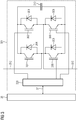
- the structure of a module 201 is shown as an example.
- the module is designed as a half-bridge module 201.
- the module 201 has a first switchable and switchable electronic switching element 202 (switchable and switchable switching element 202) with a first anti-parallel diode 204.
- the module 201 has a second electronic switching element 206 that can be switched on and off (switching element 206 that can be switched on and off) with a second diode 208 connected in anti-parallel and an electrical energy store 210 in the form of a capacitor 210.
- the first electronic switching element 202 and the second electronic switching element 206 are each designed as an IGBT (insulated-gate bipolar transistor).
- the first electronic switching element 202 is electrically connected in series with the second electronic switching element 206.
- a first galvanic module connection 212 is arranged at the connection point between the two electronic switching elements 202 and 206.
- a second galvanic module connection 215 is arranged at the connection of the second switching element 206, which lies opposite the connection point.
- the second module connection 215 is also connected to a first connection of the energy store 210; a second connection of the energy store 210 is electrically connected to the connection of the first switching element 202, which is opposite the connection point.
- the energy store 210 is therefore electrically connected in parallel to the series circuit comprising the first switching element 202 and the second switching element 206.
- the module-internal electronic module control device 220 By appropriate activation of the first switching element 202 and the second switching element 206 by the module-internal electronic module control device 220, it can be achieved that between the first galvanic module connection 212 and the second galvanic module connection 215 either the voltage of the energy store 210 is output or no voltage is output (ie a zero voltage is output).
- the desired output voltage of the converter can thus be generated by the interaction of the modules of the individual phase module branches.
- FIG. 3 A further exemplary embodiment of a module 301 of the modular multilevel converter 1 is shown.
- This module 301 can be, for example, module 1_2 (or one of the other modules in FIG Figure 1 modules shown).
- the known first switching element 202, second switching element 206, first diode 204, second diode 208 and energy store 210 have the in Figure 3
- the module 301 shown has a third electronic switching element 302 that can be switched on and off with an antiparallel connected third diode 304 and a fourth electronic switching element 306 that can be switched on and off with an antiparallel connected fourth diode 308.
- the third switching element 302 that can be switched on and off and the fourth switching element 306 that can be switched on and off are each designed as an IGBT.
- the second galvanic module connection 315 is not electrically connected to the second switching element 206, but to a center point of an electrical series connection of the third switching element 302 and the fourth switching element 306.
- Module 301 of the Figure 3 is a so-called full-bridge module 301.
- This full-bridge module 301 is characterized in that, with appropriate control of the four switching elements between the first galvanic module connection 212 and the second galvanic module connection 315, either the positive voltage of the energy store 210, the negative voltage of the Energy storage 210 or a voltage of zero value (zero voltage) can be output.
- the polarity of the output voltage can be reversed by means of the full bridge module 301.
- the converter 1 can either only half-bridge modules 201, only full-bridge modules 301 or also half-bridge modules 201 and full-bridge modules 301. Large electrical currents of the converter flow via the first galvanic module connection 212 and the second galvanic module connection 215, 315.
- FIG. 4 an embodiment of a high-voltage direct current transmission system 401 is shown schematically.
- This high-voltage direct current transmission system 401 has two power converters 1, as shown in FIG Figure 1 are shown. These two converters 1 are electrically connected to one another on the DC voltage side via a high-voltage DC connection 405.
- the two positive DC voltage connections 16 of the converter 1 are electrically connected to one another by means of a first high-voltage DC line 405a; the two negative direct voltage connections 17 of the two converters 1 are electrically connected to one another by means of a second high-voltage direct current line 405b.
- Such a high-voltage direct current transmission system 401 can transmit electrical energy over long distances; the high-voltage direct current connection 405 then has a corresponding length.
- FIG. 5 An exemplary embodiment of a converter 501 is shown, which serves as a reactive power compensator 501.
- This converter 501 only has the three phase module branches 11, 18 and 27, which form three phase modules 505, 507 and 509 of the converter.
- the number of phase modules 505, 507 and 509 corresponds to the number of phases of an AC network 511 to which the converter 501 is connected.
- the three phase module branches 11, 18 and 27 are connected to one another in a star shape.
- the end of the three phase module branches opposite the star point is electrically connected to a phase line 515, 517 and 519 of the three-phase AC voltage network 511.
- the three phase modules 505, 507 and 509 can be in another
- the exemplary embodiment can also be connected in a delta connection instead of in a star connection.
- the converter 501 can supply the AC voltage network 511 with reactive power or take reactive power from the AC voltage network 511.
- the energy store 210 is an electrical capacitor 210, more precisely a unipolar electrical capacitor (with a positive capacitor connection (+) and a negative capacitor connection (-)).
- the energy store 210 can also be a different type of capacitor, an electric battery or an electric accumulator.
- the arrangement 602 can, for example, be the module 1_2 (or one of the other modules in FIG Figure 1 modules shown).
- the arrangement 602 has the basic structure of the in Figure 2 module 201 shown.
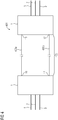
- the electrical energy store 210 is connected to an electronic circuit 612 (power electronic circuit 612) by means of a first electrical conductor 606 (first electrical connection 606) and a second electrical conductor 608 (second electrical connection 608).
- the first electrical conductor 606 is a positive electrical conductor; the second electrical conductor 608 is a negative electrical conductor.
- the electronic circuit 612 has the first electronic switching element 202, the second electronic switching element 206, the first antiparallel connected diode 204 and the second antiparallel connected diode 208, which already consists of the Figure 2 are known.
- the arrangement 602 furthermore has a thyristor 616, which is connected in parallel with the electrical energy store 210.
- An anode 620 (anode terminal 620) of the thyristor is electrically connected to the first electrical conductor 606.
- a cathode 622 (cathode connection 622) of the thyristor is electrically connected connected to the second electrical conductor 608.
- a gate 624 (gate connection 624) of the thyristor is not connected in the exemplary embodiment.
- the thyristor 616 is a protective thyristor 616 for carrying a discharge current 630 of the electrical energy store 210 in the event of a fault. In the event of a fault, the thyristor 616 conducts the discharge current 630 of the electrical energy store 210 past the electronic circuit 612 and thus protects the electronic circuit 612 from the (generally very high) discharge current 630 of the electrical energy store 210. Such a thyristor is also called a crowbar Designated thyristor.
- the discharge current 630 can also be referred to as a short-circuit-like discharge current 630 or as a short-circuit current 630.
- the following procedure takes place in the arrangement 602 in the event of a fault: It is assumed as a starting point that the electrical energy store 210 is charged. The thyristor 616 is switched off (not fired), that is to say the thyristor 616 blocks the current flow. Thereupon, an error occurs in the electronic circuit 612: For example, (undesirably) the first electronic switching element 202 and the second electronic switching element 206 simultaneously become electrically conductive (a so-called bridge short-circuit occurs in the through the first electronic switching element 202 and the second electronic switching element 206 formed half-bridge). As a result, the electrical energy store 210 is short-circuited and the discharge current 630 suddenly begins to flow.
- the discharge current 630 initially flows from the energy store 210 via the first electrical conductor 606 to the electronic circuit 612. There, the discharge current 630 flows via the first electronic switching element 202 and the second electronic switching element 206. The discharge current 630 then flows via the second electrical conductor 608 back to the energy store 210 Charging current in the first electrical conductor 606 and in the second electrical conductor 608 in opposite directions.
- the discharge current 630 is only limited by stray capacitances and ohmic resistances which occur in the first electrical conductor, the second electrical conductor and the electronic circuit 612. Therefore, the discharge current 630 increases relatively quickly.
- a time-changing magnetic field is generated around the first electrical conductor 606. Due to the discharge current 630, a time-changing magnetic field is also generated around the second electrical conductor 608. These two magnetic fields overlap and both penetrate the thyristor 616 and thus the semiconductor material of the thyristor 616.
- the thyristor is namely spatially adjacent to the first electrical conductor and the second electrical conductor.
- the thyristor 616 has an outer housing made of anti-magnetic material, which does not or only slightly impedes the magnetic field penetrating the thyristor 616.
- the time-changing magnetic field induces a current in the semiconductor material of the thyristor, for example an eddy current.
- This current acts as a gate current (internal gate current, internal gate current) or ignition current and causes the thyristor 616 to turn on (ie, to fire the thyristor 616). Due to the switching on of the thyristor 616, the discharge current 630 no longer flows via the electronic circuit 612, but rather via the thyristor 616.
- the discharge current 630 now flows from the energy store 210 via part of the first electrical conductor 606 to the anode 620 of the thyristor and from the cathode 622 of the thyristor via part of the second electrical conductor 608 back to the energy store 210.
- the discharge current 630 flows through the thyristor 616 because the thyristor 616 is electrically connected to the energy store 210 in a low-inductance manner. That is, the electrical The connection between the thyristor 616 and the energy store 210 has a lower electrical inductance than the first electrical conductor 606 and the second electrical conductor 608, which connect the energy store 210 to the electronic circuit 612.
- the thyristor 616 is thus switched on by the induced current (eddy current).
- the gate 624 can be unconnected.
- the gate 624 does not even have to be led out of the thyristor.
- the thyristor is only switched on by the induced current (gate current or ignition current) when the change in the magnetic field over time exceeds a threshold value.
- the decisive factor here is the temporal change in the magnetic field at the location of the semiconductor material of the thyristor. Particularly large temporal changes in the magnetic field can be realized on the semiconductor material of the thyristor if the thyristor is arranged very close to the first electrical conductor 606 and / or to the second electrical conductor 608.
- the induced current turns the thyristor on when the temporal change in the discharge current (in the first electrical conductor 606 and / or the second electrical conductor 608) exceeds a threshold value.
- This threshold value can be, for example, between 5 and 50 kA per ⁇ s.
- the thyristor 616 Due to the discharge current 630 flowing through the thyristor 616, the thyristor 616 can be thermally overloaded and thereby destroyed. In the event of a fault, the thyristor thus acts as a sacrificial element in order to protect the electronic circuit 612 from the discharge current 630. After an error occurs (ie after discharging the discharge current 630 via the thyristor 616), the thyristor 616 must be replaced.
- the thyristor 616 has a so-called conduct-on-fail property, that is to say that in the event of a fault (and also in the event of destruction due to overload), the thyristor 616 remains conductive and is therefore able to continue to discharge current 630 until it decays to lead.
- conductors-on-fail thyristors are commercially available.
- the gate 624 can also be terminated by means of a non-zero constant impedance.
- a control unit can also be connected to the gate 624 which, in the event of a discharge-free fault (i.e. a fault which does not go along with a discharge of the energy store 210 or with a short-circuit-like discharge current 630 of the energy store), a gate current into the gate 624 of the thyristor feeds.
- a discharge-free fault can, for example, be an overcharge of the energy store 210, which does not lead directly to a short-circuit-like discharge current 630, but should nevertheless be prevented.
- FIG. 7 Another embodiment of an arrangement 702 is shown.
- the arrangement 702 can, for example, be the module 1_2 (or one of the other modules in FIG Figure 1 modules shown).
- the arrangement 702 has the basic structure of the in Figure 3 module 301 shown.
- the arrangement 702 differs from the arrangement 602 of FIG Figure 6 only in that the arrangement 702 has an electronic circuit 712 that differs from the electronic circuit 612: the electronic circuit 712 additionally has a third electronic switching element 302 with a third diode 304 connected in antiparallel and a fourth electronic switching element 306 with a fourth diode 308 connected in anti-parallel.
- the first electronic switching element 202, the second electronic switching element 206, the third electronic switching element 302 and the fourth electronic switching element 306 are connected in a full-bridge circuit. For example, an error can occur in the electronic circuit 712, which results in the third electronic switching element 302 and the fourth electronic switching element 306 simultaneously becoming electrically conductive.
- the third switching element 302 and the fourth switching element 306 electrically short-circuit the energy store 210 and the discharge current 630 begins to flow from the energy store 210 to the electronic circuit 712.
- the rest of the procedure corresponds to that in connection with Figure 6 explained method.
- FIG 8 An embodiment of an arrangement 802 of the thyristor 616 between the first electrical conductor 606 and the second electrical conductor 608 is shown.
- the first electrical conductor 606 and the second electrical conductor 608 are configured here as a first busbar 606 and a second busbar 608.
- the first electrical busbar 606 and the second electrical busbar 608 each have a flat profile.
- electronic circuit 612 is shown schematically as block 612; in the right part of the Figure 8
- the energy store 210 is shown schematically as a block 210.
- the electronic circuit 712 can also be used.
- the first electrical conductor 606 (first electrical busbar 606) connects the energy store 210 to the electronic circuit 612.
- the second electrical conductor 608 (second electrical busbar 608) connects the energy store 210 to the electronic circuit 612.
- the thyristor 616 is mechanically clamped.
- the thyristor 616 is thus in the Gap 635 between the first electrical conductor 606 and the second electrical conductor 608.
- the anode 620 of the thyristor 616 lies on the first electrical conductor 606, the cathode 622 of the thyristor 616 lies on the second electrical conductor 608.
- the tensioning is realized by means of a tensioning device 806.
- the clamping device 806 has two bolts which mechanically clamp the first electrical conductor 606, the thyristor 616 and the second electrical conductor 608 by means of a nut in each case.
- the first electrical conductor 606, the thyristor 616 and the second electrical conductor 608 form a clamping assembly.
- This tension bandage or the mechanical bracing bring about good electrical contact between the first electrical conductor 60 and the thyristor 616 and good electrical contact between the second electrical conductor 608 and the thyristor 616.
- the arrangement is mechanically stable due to the bracing or the tension bandage, that the arrangement can reliably absorb the current forces acting due to the large discharge current.
- the overall height of the thyristor 616 roughly corresponds to the distance between the first electrical conductor 606 and the second electrical conductor 608.
- the anode 620 and the cathode 622 each form a clamping surface of the thyristor 616.
- the field lines of the magnetic flux density B run parallel to the clamping surfaces of the thyristor 616 (in Figure 8 not shown; see. Figure 10 ).
- the electric field (E field) is perpendicular to the field of magnetic flux density B, but is not shown in the figures.
- the thyristor 616 can be switched on by means of a discharge current 630, which rises very quickly from zero to approx. 20 kA, that is, a discharge current with a maximum value greater than approx. 20 kA, which is very short ( less than 1 ⁇ s - 2ps) increases to its maximum value, leads to the thyristor 616 being switched on.
- the thyristor 616 has the Figure 8 the shape of a disc cell; the thyristor 616 has a disk cell housing 810.
- the thyristor has a disk-shaped shape, the base area forming the cathode and the cover area forming the anode.
- Such disk-cell-shaped thyristors can be used, in particular, to implement mechanically stable clamping associations.
- the representation of the Figure 8 also shows that gate 624 of the thyristor is not connected. In contrast to the representation of the Figure 8 the gate 624 need not be led out of the housing 810 of the thyristor 616 because it is not connected.
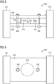
- Figure 9 is the arrangement 802 according to the Figure 8 shown in a side view.
- the circumference of the disk-cell-shaped thyristor 616 is indicated by a dashed line.
- the arrangement 802 is shown in a top view, similar to the illustration in FIG Figure 8 .
- the tensioner 806, the housing of the thyristor 616 and the electrical connections between the anode and the first electrical conductor and between the cathode and the second electrical conductor have been omitted; only the semiconductor material 1006 of the thyristor 616 is shown.
- This semiconductor material 1006 forms a disk 1006 (disk-shaped semiconductor material 1006, semiconductor material disk 1006).
- the disk 1006 is shown in cross section. In the side view, the disk 1006 has a circular shape similar to that in FIG Figure 9 the circumference of the thyristor 616.
- the semiconductor material 1006 is shown exaggeratedly thick for reasons of better representability.
- the relevant semiconductor structures (in particular silicon structures) in this semiconductor material 1006 are often very thin, for example only several 100 ⁇ m thick.
- the field lines of the magnetic field 1010 are shown, which form in the space 635 between the first electrical conductor 606 and the second electrical conductor 608 (field lines 1010 of the magnetic flux density B).
- the field lines 1010 of the magnetic field come out of the plane of the drawing and point to the viewer; the viewer looks, so to speak, from the front onto the field line tip. Since the first electrical conductor 606 and the second electrical conductor 608 are plate-shaped, parallel field lines 1010 are formed in the space 635 between the first electrical conductor 606 and the second electrical conductor 608.
- the field lines 1010 penetrate the semiconductor material 1006 of the thyristor.
- a voltage 1016 is induced in the semiconductor material 1006, which results in the flow of a current 1018 (eddy current 1018) in the semiconductor material 1006 of the thyristor.
- the voltage 1016 and the current 1018 are only shown schematically here.
- the induced current 1018 acts as a gate current 1018 of the thyristor or as an ignition current of the thyristor and turns on the thyristor 616 (i.e., the current 1018 fires the thyristor 616).
- the first electrical conductor 606 has a first flat outer surface 1024.
- the second electrical conductor 608 has a second flat outer surface 1026.
- the first flat outer surface 1024 and the second flat outer surface 1026 are arranged parallel to one another.
- the disk-shaped semiconductor material 1006 of the thyristor 616 is arranged parallel to the first outer surface 1024 and also parallel to the second outer surface 2026. This arrangement of the semiconductor material 1006 enables a compact and mechanically stable structure of the arrangement 802. In addition (due to the possible small distance between the first electrical conductor 606 and the second electrical conductor 608) there is a large temporal change in the magnetic field at the location of the semiconductor material 1006.
- the disk 1006 (the silicon wafer 1006 of the thyristor) is a conductive material.
- the current 1018 (in particular an eddy current) is generated in the area of the disk. generated. This current causes the thyristor 616 to fire, that is, to turn on.
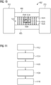
- Figure 11 the method for discharging the energy store is shown again by means of a flow chart.
- the starting point of the method is that the energy store is charged and the thyristor is in the switched-off state (blocking state).
- the discharge current 630 of the energy store 210 begins to flow.
- the discharge current 630 flows back from the energy store 210 via the first electrical conductor 606 to the electronic circuit 612 and via the second electrical conductor 608 to the energy store 210.
- the current 1018 can act as a gate current or as an ignition current of the thyristor.
- the discharge current 630 of the energy store 210 then flows through the thyristor 616 and is thereby bypassed the electronic circuit 612.
- the magnetic field coupled into the thyristor passes through the entire thyristor and generates an induced current (eddy current) in the thin semiconductor structure / semiconductor material of the thyristor. From a threshold value of the change in the magnetic field over time (dB / dt), this current is sufficient to allow a gate current (or an ignition current) to flow in the semiconductor material and thereby switch on the thyristor (without the need for an external gate current from an external electronic evaluation circuit is). An external control of the gate is not necessary, the error detection / short circuit detection is inherent in the thyristor and works as long as the thyristor is intact.
- the arrangement and the method have a low failure rate (FIT rate), which essentially corresponds to the failure rate of thyristors. This failure rate is very low with thyristors.
- the short-circuit-like discharge current 630 of the energy store is used for instantaneous ignition of the thyristor without the need for a detection circuit or evaluation circuit, which would always result in a time delay.
- the technical Realization using only one thyristor is extremely simple and inexpensive. When the thyristor is ignited, it can be destroyed (depending on the amount of energy to be controlled in the energy store) and may have to be replaced during later maintenance.
- a comparatively simple diode disk cell housing can be used for the thyristor, since the gate connection 624 is not used and consequently does not need to be led out of the housing.
Landscapes
- Engineering & Computer Science (AREA)
- Power Engineering (AREA)
- Inverter Devices (AREA)
- Rectifiers (AREA)
- Generation Of Surge Voltage And Current (AREA)
Priority Applications (1)
| Application Number | Priority Date | Filing Date | Title |
|---|---|---|---|
| PL16765942T PL3485565T3 (pl) | 2016-09-05 | 2016-09-05 | Sposób wyładowania elektrycznego zasobnika energii |
Applications Claiming Priority (1)
| Application Number | Priority Date | Filing Date | Title |
|---|---|---|---|
| PCT/EP2016/070832 WO2018041370A1 (de) | 2016-09-05 | 2016-09-05 | Verfahren zum entladen eines elektrischen energiespeichers |
Publications (2)
| Publication Number | Publication Date |
|---|---|
| EP3485565A1 EP3485565A1 (de) | 2019-05-22 |
| EP3485565B1 true EP3485565B1 (de) | 2020-05-27 |
Family
ID=56926162
Family Applications (1)
| Application Number | Title | Priority Date | Filing Date |
|---|---|---|---|
| EP16765942.4A Active EP3485565B1 (de) | 2016-09-05 | 2016-09-05 | Verfahren zum entladen eines elektrischen energiespeichers |
Country Status (8)
| Country | Link |
|---|---|
| US (1) | US10461663B2 (pl) |
| EP (1) | EP3485565B1 (pl) |
| JP (1) | JP6731543B2 (pl) |
| KR (1) | KR102269017B1 (pl) |
| CN (1) | CN109661768B (pl) |
| ES (1) | ES2812876T3 (pl) |
| PL (1) | PL3485565T3 (pl) |
| WO (1) | WO2018041370A1 (pl) |
Cited By (1)
| Publication number | Priority date | Publication date | Assignee | Title |
|---|---|---|---|---|
| WO2023155979A1 (de) * | 2022-02-16 | 2023-08-24 | Siemens Energy Global GmbH & Co. KG | Modul eines modularen multilevelstromrichters |
Families Citing this family (10)
| Publication number | Priority date | Publication date | Assignee | Title |
|---|---|---|---|---|
| EP3381109B1 (de) * | 2016-01-19 | 2022-03-09 | Siemens Energy Global GmbH & Co. KG | Multilevelumrichter |
| PL3485563T3 (pl) * | 2016-09-01 | 2020-10-19 | Siemens Aktiengesellschaft | Układ przetwornicy jak również sposób jej pracy |
| DE102018211900A1 (de) * | 2018-07-17 | 2020-01-23 | Siemens Aktiengesellschaft | Halbleiteranordnung, Schaltmodul mit der Halbleiteranordnung und modularer Mehrstufenumrichter mit dem Schaltmodul |
| EP3621189B1 (en) * | 2018-09-06 | 2021-04-21 | ABB Power Grids Switzerland AG | Modular dc crowbar |
| EP3931958A1 (en) * | 2019-02-28 | 2022-01-05 | ABB Power Grids Switzerland AG | Converter cell with crowbar |
| WO2020173566A1 (en) | 2019-02-28 | 2020-09-03 | Abb Schweiz Ag | Converter cell with crowbar |
| WO2021028003A1 (en) * | 2019-08-13 | 2021-02-18 | Vestas Wind Systems A/S | Intelligent discharge control for modular multilevel converter |
| EP3783783B1 (de) * | 2019-08-23 | 2025-04-23 | Siemens Energy Global GmbH & Co. KG | Anordnung zum regeln eines leistungsflusses in einem wechselspannungsnetz und verfahren zum schutz der anordnung |
| EP4040659A1 (en) * | 2021-02-09 | 2022-08-10 | General Electric Technology GmbH | Electrical assembly |
| EP4348819A1 (en) * | 2021-05-25 | 2024-04-10 | Hitachi Energy Ltd | Power electronic building block for modular multilevel converters |
Family Cites Families (15)
| Publication number | Priority date | Publication date | Assignee | Title |
|---|---|---|---|---|
| JPS5221871B2 (pl) * | 1971-11-29 | 1977-06-14 | ||
| EP1427107B1 (fr) | 2002-12-04 | 2011-09-14 | STMicroelectronics S.A. | Commutateur de type SCR commande en HF |
| JP2006332304A (ja) * | 2005-05-26 | 2006-12-07 | Matsushita Electric Works Ltd | 半導体リレー装置 |
| DE102005040543A1 (de) | 2005-08-26 | 2007-03-01 | Siemens Ag | Stromrichterschaltung mit verteilten Energiespeichern |
| US7602157B2 (en) * | 2005-12-28 | 2009-10-13 | Flyback Energy, Inc. | Supply architecture for inductive loads |
| ES2710557T3 (es) * | 2011-09-29 | 2019-04-25 | Siemens Ag | Protección de corriente de cortocircuito para un submódulo de un convertidor multinivel modular (MMC) |
| CN102694458A (zh) * | 2012-05-29 | 2012-09-26 | 北京金自天正智能控制股份有限公司 | 一种交直交变流器的快速放电保护电路 |
| DE102014200108A1 (de) * | 2014-01-08 | 2015-07-09 | Siemens Aktiengesellschaft | Umrichter zwischen Gleichspannung und Wechselspannung zur Anwendung in der Hochspannungs-Gleichstrom-Übertragung und Verfahren zur Spannungsumrichtung |
| WO2015133365A1 (ja) * | 2014-03-05 | 2015-09-11 | 三菱電機株式会社 | 電力変換装置 |
| CN208433908U (zh) * | 2015-05-28 | 2019-01-25 | 西门子公司 | 电压源换流器模块和换流器 |
| EP3381109B1 (de) * | 2016-01-19 | 2022-03-09 | Siemens Energy Global GmbH & Co. KG | Multilevelumrichter |
| CN108702083B (zh) * | 2016-02-12 | 2020-09-18 | Abb电网瑞士股份公司 | 用于hvdc功率站的转换器模块 |
| KR102600766B1 (ko) * | 2016-09-22 | 2023-11-13 | 엘에스일렉트릭(주) | 모듈형 멀티레벨 컨버터 |
| DE102017123348A1 (de) * | 2017-10-09 | 2019-04-11 | Dr. Ing. H.C. F. Porsche Aktiengesellschaft | Wechselrichter für ein Elektroauto |
| DE102017219499A1 (de) * | 2017-11-02 | 2019-05-02 | Siemens Aktiengesellschaft | Elektrische Anordnung mit Teilmodulen sowie Teilmodule als solche |
-
2016
- 2016-09-05 ES ES16765942T patent/ES2812876T3/es active Active
- 2016-09-05 PL PL16765942T patent/PL3485565T3/pl unknown
- 2016-09-05 US US16/329,958 patent/US10461663B2/en active Active
- 2016-09-05 CN CN201680088965.8A patent/CN109661768B/zh active Active
- 2016-09-05 WO PCT/EP2016/070832 patent/WO2018041370A1/de not_active Ceased
- 2016-09-05 KR KR1020197009495A patent/KR102269017B1/ko active Active
- 2016-09-05 EP EP16765942.4A patent/EP3485565B1/de active Active
- 2016-09-05 JP JP2019511978A patent/JP6731543B2/ja active Active
Non-Patent Citations (1)
| Title |
|---|
| None * |
Cited By (1)
| Publication number | Priority date | Publication date | Assignee | Title |
|---|---|---|---|---|
| WO2023155979A1 (de) * | 2022-02-16 | 2023-08-24 | Siemens Energy Global GmbH & Co. KG | Modul eines modularen multilevelstromrichters |
Also Published As
| Publication number | Publication date |
|---|---|
| KR102269017B1 (ko) | 2021-06-25 |
| WO2018041370A1 (de) | 2018-03-08 |
| CN109661768A (zh) | 2019-04-19 |
| KR20190041530A (ko) | 2019-04-22 |
| EP3485565A1 (de) | 2019-05-22 |
| US10461663B2 (en) | 2019-10-29 |
| JP2019527018A (ja) | 2019-09-19 |
| US20190199237A1 (en) | 2019-06-27 |
| JP6731543B2 (ja) | 2020-07-29 |
| CN109661768B (zh) | 2021-02-05 |
| ES2812876T3 (es) | 2021-03-18 |
| PL3485565T3 (pl) | 2020-11-16 |
Similar Documents
| Publication | Publication Date | Title |
|---|---|---|
| EP3485565B1 (de) | Verfahren zum entladen eines elektrischen energiespeichers | |
| EP2118993B1 (de) | Verfahren zur schadenbegrenzung eines leistungshalbleiter aufweisenden stromrichters bei einem kurzschluss im gleichspannungszwischenkreis | |
| EP3072143B1 (de) | Vorrichtung zum schalten eines gleichstroms | |
| EP3259839B1 (de) | Umrichteranordnung sowie verfahren zu deren kurzschlussschutz | |
| DE4235329C2 (de) | Kurzschlußeinrichtung, insbesondere zum Löschen von Störlichtbögen in Niederspannungs-Schaltanlagen zur Verteilung elektrischer Energie, Anordnung und Verwendung hierfür | |
| EP2643930B1 (de) | Schaltungsanordnungen für elektronisch gesteuerte dc-netze | |
| EP2678926A2 (de) | Submodul eines modularen mehrstufenumrichters | |
| WO2016188589A1 (de) | Spannungsgeführtes stromrichtermodul | |
| WO2019011642A1 (de) | Elektronischer schalter mit überspannungsbegrenzer | |
| EP3622621B1 (de) | Multilevelstromrichter | |
| EP3468831B1 (de) | Antriebssystem für ein schienenfahrzeug | |
| EP3830921B1 (de) | Sternpunkterdung mit überspannungsbegrenzung für einen mehrphasigen transformator | |
| DE102019107112B3 (de) | Schaltvorrichtung, Spannungsversorgungssystem, Verfahren zum Betreiben einer Schaltvorrichtung und Herstellverfahren | |
| EP3622619B1 (de) | Elektrische kurzschliesseinrichtung | |
| WO2018113926A1 (de) | Stromrichter | |
| EP3818549B1 (de) | Anordnung mit einem modul eines multilevelstromrichters | |
| EP3588706B1 (de) | Funkenstreckenanordnung mit zwei zündkreisen | |
| WO2022229056A1 (de) | Laststufenschaltermodul, anordnung aus laststufenschaltermodul und leistungstransformator und verfahren zum betrieb eines laststufenschaltermoduls | |
| EP4457925A1 (de) | Modul eines modularen multilevelstromrichters | |
| EP3087572B1 (de) | Elektrisches bauelement | |
| EP3598628A1 (de) | Halbleiteranordnung, schaltmodul mit der halbleiteranordnung und modularer mehrstufenumrichter mit dem schaltmodul | |
| DE2057722C3 (de) | Überspannungsschutz anordnung | |
| DE3408788A1 (de) | Elektronische sicherungsvorrichtung fuer halbleiterschalter zum schutz gegen ueberstrom | |
| EP4222832A1 (de) | Anordnung mit einer gleichstrom-übertragungsleitung | |
| DE102023105115A1 (de) | Elektronische schaltung zum abschalten von halbleiterschaltern bei kritischen strömen |
Legal Events
| Date | Code | Title | Description |
|---|---|---|---|
| STAA | Information on the status of an ep patent application or granted ep patent |
Free format text: STATUS: THE INTERNATIONAL PUBLICATION HAS BEEN MADE |
|
| PUAI | Public reference made under article 153(3) epc to a published international application that has entered the european phase |
Free format text: ORIGINAL CODE: 0009012 |
|
| STAA | Information on the status of an ep patent application or granted ep patent |
Free format text: STATUS: REQUEST FOR EXAMINATION WAS MADE |
|
| 17P | Request for examination filed |
Effective date: 20190206 |
|
| AK | Designated contracting states |
Kind code of ref document: A1 Designated state(s): AL AT BE BG CH CY CZ DE DK EE ES FI FR GB GR HR HU IE IS IT LI LT LU LV MC MK MT NL NO PL PT RO RS SE SI SK SM TR |
|
| AX | Request for extension of the european patent |
Extension state: BA ME |
|
| REG | Reference to a national code |
Ref country code: DE Ref legal event code: R079 Ref document number: 502016010071 Country of ref document: DE Free format text: PREVIOUS MAIN CLASS: H02M0007490000 Ipc: H02M0007483000 |
|
| DAV | Request for validation of the european patent (deleted) | ||
| DAX | Request for extension of the european patent (deleted) | ||
| GRAP | Despatch of communication of intention to grant a patent |
Free format text: ORIGINAL CODE: EPIDOSNIGR1 |
|
| STAA | Information on the status of an ep patent application or granted ep patent |
Free format text: STATUS: GRANT OF PATENT IS INTENDED |
|
| RIC1 | Information provided on ipc code assigned before grant |
Ipc: H02M 7/483 20070101AFI20191203BHEP Ipc: H03K 17/723 20060101ALI20191203BHEP Ipc: H03K 17/0814 20060101ALI20191203BHEP |
|
| INTG | Intention to grant announced |
Effective date: 20200103 |
|
| GRAS | Grant fee paid |
Free format text: ORIGINAL CODE: EPIDOSNIGR3 |
|
| GRAA | (expected) grant |
Free format text: ORIGINAL CODE: 0009210 |
|
| STAA | Information on the status of an ep patent application or granted ep patent |
Free format text: STATUS: THE PATENT HAS BEEN GRANTED |
|
| AK | Designated contracting states |
Kind code of ref document: B1 Designated state(s): AL AT BE BG CH CY CZ DE DK EE ES FI FR GB GR HR HU IE IS IT LI LT LU LV MC MK MT NL NO PL PT RO RS SE SI SK SM TR |
|
| REG | Reference to a national code |
Ref country code: GB Ref legal event code: FG4D Free format text: NOT ENGLISH |
|
| REG | Reference to a national code |
Ref country code: CH Ref legal event code: EP |
|
| REG | Reference to a national code |
Ref country code: DE Ref legal event code: R096 Ref document number: 502016010071 Country of ref document: DE |
|
| REG | Reference to a national code |
Ref country code: AT Ref legal event code: REF Ref document number: 1275606 Country of ref document: AT Kind code of ref document: T Effective date: 20200615 |
|
| REG | Reference to a national code |
Ref country code: CH Ref legal event code: NV Representative=s name: SIEMENS SCHWEIZ AG, CH |
|
| REG | Reference to a national code |
Ref country code: SE Ref legal event code: TRGR |
|
| REG | Reference to a national code |
Ref country code: LT Ref legal event code: MG4D Ref country code: NO Ref legal event code: T2 Effective date: 20200527 |
|
| PG25 | Lapsed in a contracting state [announced via postgrant information from national office to epo] |
Ref country code: IS Free format text: LAPSE BECAUSE OF FAILURE TO SUBMIT A TRANSLATION OF THE DESCRIPTION OR TO PAY THE FEE WITHIN THE PRESCRIBED TIME-LIMIT Effective date: 20200927 Ref country code: FI Free format text: LAPSE BECAUSE OF FAILURE TO SUBMIT A TRANSLATION OF THE DESCRIPTION OR TO PAY THE FEE WITHIN THE PRESCRIBED TIME-LIMIT Effective date: 20200527 Ref country code: PT Free format text: LAPSE BECAUSE OF FAILURE TO SUBMIT A TRANSLATION OF THE DESCRIPTION OR TO PAY THE FEE WITHIN THE PRESCRIBED TIME-LIMIT Effective date: 20200928 Ref country code: GR Free format text: LAPSE BECAUSE OF FAILURE TO SUBMIT A TRANSLATION OF THE DESCRIPTION OR TO PAY THE FEE WITHIN THE PRESCRIBED TIME-LIMIT Effective date: 20200828 Ref country code: LT Free format text: LAPSE BECAUSE OF FAILURE TO SUBMIT A TRANSLATION OF THE DESCRIPTION OR TO PAY THE FEE WITHIN THE PRESCRIBED TIME-LIMIT Effective date: 20200527 |
|
| REG | Reference to a national code |
Ref country code: NL Ref legal event code: MP Effective date: 20200527 |
|
| PG25 | Lapsed in a contracting state [announced via postgrant information from national office to epo] |
Ref country code: BG Free format text: LAPSE BECAUSE OF FAILURE TO SUBMIT A TRANSLATION OF THE DESCRIPTION OR TO PAY THE FEE WITHIN THE PRESCRIBED TIME-LIMIT Effective date: 20200827 Ref country code: RS Free format text: LAPSE BECAUSE OF FAILURE TO SUBMIT A TRANSLATION OF THE DESCRIPTION OR TO PAY THE FEE WITHIN THE PRESCRIBED TIME-LIMIT Effective date: 20200527 Ref country code: LV Free format text: LAPSE BECAUSE OF FAILURE TO SUBMIT A TRANSLATION OF THE DESCRIPTION OR TO PAY THE FEE WITHIN THE PRESCRIBED TIME-LIMIT Effective date: 20200527 Ref country code: HR Free format text: LAPSE BECAUSE OF FAILURE TO SUBMIT A TRANSLATION OF THE DESCRIPTION OR TO PAY THE FEE WITHIN THE PRESCRIBED TIME-LIMIT Effective date: 20200527 |
|
| REG | Reference to a national code |
Ref country code: DE Ref legal event code: R081 Ref document number: 502016010071 Country of ref document: DE Owner name: SIEMENS ENERGY GLOBAL GMBH & CO. KG, DE Free format text: FORMER OWNER: SIEMENS AKTIENGESELLSCHAFT, 80333 MUENCHEN, DE |
|
| PG25 | Lapsed in a contracting state [announced via postgrant information from national office to epo] |
Ref country code: AL Free format text: LAPSE BECAUSE OF FAILURE TO SUBMIT A TRANSLATION OF THE DESCRIPTION OR TO PAY THE FEE WITHIN THE PRESCRIBED TIME-LIMIT Effective date: 20200527 Ref country code: NL Free format text: LAPSE BECAUSE OF FAILURE TO SUBMIT A TRANSLATION OF THE DESCRIPTION OR TO PAY THE FEE WITHIN THE PRESCRIBED TIME-LIMIT Effective date: 20200527 |
|
| RAP2 | Party data changed (patent owner data changed or rights of a patent transferred) |
Owner name: SIEMENS ENERGY GLOBAL GMBH & CO. KG |
|
| PG25 | Lapsed in a contracting state [announced via postgrant information from national office to epo] |
Ref country code: DK Free format text: LAPSE BECAUSE OF FAILURE TO SUBMIT A TRANSLATION OF THE DESCRIPTION OR TO PAY THE FEE WITHIN THE PRESCRIBED TIME-LIMIT Effective date: 20200527 Ref country code: EE Free format text: LAPSE BECAUSE OF FAILURE TO SUBMIT A TRANSLATION OF THE DESCRIPTION OR TO PAY THE FEE WITHIN THE PRESCRIBED TIME-LIMIT Effective date: 20200527 Ref country code: SM Free format text: LAPSE BECAUSE OF FAILURE TO SUBMIT A TRANSLATION OF THE DESCRIPTION OR TO PAY THE FEE WITHIN THE PRESCRIBED TIME-LIMIT Effective date: 20200527 Ref country code: RO Free format text: LAPSE BECAUSE OF FAILURE TO SUBMIT A TRANSLATION OF THE DESCRIPTION OR TO PAY THE FEE WITHIN THE PRESCRIBED TIME-LIMIT Effective date: 20200527 Ref country code: CZ Free format text: LAPSE BECAUSE OF FAILURE TO SUBMIT A TRANSLATION OF THE DESCRIPTION OR TO PAY THE FEE WITHIN THE PRESCRIBED TIME-LIMIT Effective date: 20200527 |
|
| PG25 | Lapsed in a contracting state [announced via postgrant information from national office to epo] |
Ref country code: SK Free format text: LAPSE BECAUSE OF FAILURE TO SUBMIT A TRANSLATION OF THE DESCRIPTION OR TO PAY THE FEE WITHIN THE PRESCRIBED TIME-LIMIT Effective date: 20200527 |
|
| REG | Reference to a national code |
Ref country code: DE Ref legal event code: R097 Ref document number: 502016010071 Country of ref document: DE |
|
| REG | Reference to a national code |
Ref country code: ES Ref legal event code: FG2A Ref document number: 2812876 Country of ref document: ES Kind code of ref document: T3 Effective date: 20210318 |
|
| PLBE | No opposition filed within time limit |
Free format text: ORIGINAL CODE: 0009261 |
|
| STAA | Information on the status of an ep patent application or granted ep patent |
Free format text: STATUS: NO OPPOSITION FILED WITHIN TIME LIMIT |
|
| 26N | No opposition filed |
Effective date: 20210302 |
|
| PG25 | Lapsed in a contracting state [announced via postgrant information from national office to epo] |
Ref country code: SI Free format text: LAPSE BECAUSE OF FAILURE TO SUBMIT A TRANSLATION OF THE DESCRIPTION OR TO PAY THE FEE WITHIN THE PRESCRIBED TIME-LIMIT Effective date: 20200527 |
|
| REG | Reference to a national code |
Ref country code: BE Ref legal event code: MM Effective date: 20200930 |
|
| PG25 | Lapsed in a contracting state [announced via postgrant information from national office to epo] |
Ref country code: LU Free format text: LAPSE BECAUSE OF NON-PAYMENT OF DUE FEES Effective date: 20200905 |
|
| PG25 | Lapsed in a contracting state [announced via postgrant information from national office to epo] |
Ref country code: IE Free format text: LAPSE BECAUSE OF NON-PAYMENT OF DUE FEES Effective date: 20200905 Ref country code: BE Free format text: LAPSE BECAUSE OF NON-PAYMENT OF DUE FEES Effective date: 20200930 |
|
| REG | Reference to a national code |
Ref country code: GB Ref legal event code: 732E Free format text: REGISTERED BETWEEN 20211202 AND 20211209 |
|
| PG25 | Lapsed in a contracting state [announced via postgrant information from national office to epo] |
Ref country code: TR Free format text: LAPSE BECAUSE OF FAILURE TO SUBMIT A TRANSLATION OF THE DESCRIPTION OR TO PAY THE FEE WITHIN THE PRESCRIBED TIME-LIMIT Effective date: 20200527 Ref country code: MT Free format text: LAPSE BECAUSE OF FAILURE TO SUBMIT A TRANSLATION OF THE DESCRIPTION OR TO PAY THE FEE WITHIN THE PRESCRIBED TIME-LIMIT Effective date: 20200527 Ref country code: CY Free format text: LAPSE BECAUSE OF FAILURE TO SUBMIT A TRANSLATION OF THE DESCRIPTION OR TO PAY THE FEE WITHIN THE PRESCRIBED TIME-LIMIT Effective date: 20200527 |
|
| PG25 | Lapsed in a contracting state [announced via postgrant information from national office to epo] |
Ref country code: MK Free format text: LAPSE BECAUSE OF FAILURE TO SUBMIT A TRANSLATION OF THE DESCRIPTION OR TO PAY THE FEE WITHIN THE PRESCRIBED TIME-LIMIT Effective date: 20200527 Ref country code: MC Free format text: LAPSE BECAUSE OF FAILURE TO SUBMIT A TRANSLATION OF THE DESCRIPTION OR TO PAY THE FEE WITHIN THE PRESCRIBED TIME-LIMIT Effective date: 20200527 |
|
| REG | Reference to a national code |
Ref country code: NO Ref legal event code: CREP Representative=s name: ONSAGERS AS, POSTBOKS 1813, VIKA, 0123 OSLO, NORGE Ref country code: NO Ref legal event code: CHAD Owner name: SIEMENS ENERGY GLOBAL GMBH & CO. KG, DE |
|
| REG | Reference to a national code |
Ref country code: AT Ref legal event code: PC Ref document number: 1275606 Country of ref document: AT Kind code of ref document: T Owner name: SIEMENS ENERGY GLOBAL GMBH & CO. KG, DE Effective date: 20221018 |
|
| P01 | Opt-out of the competence of the unified patent court (upc) registered |
Effective date: 20231222 |
|
| REG | Reference to a national code |
Ref country code: CH Ref legal event code: U11 Free format text: ST27 STATUS EVENT CODE: U-0-0-U10-U11 (AS PROVIDED BY THE NATIONAL OFFICE) Effective date: 20251001 |
|
| PGFP | Annual fee paid to national office [announced via postgrant information from national office to epo] |
Ref country code: DE Payment date: 20250926 Year of fee payment: 10 |
|
| PGFP | Annual fee paid to national office [announced via postgrant information from national office to epo] |
Ref country code: NO Payment date: 20250917 Year of fee payment: 10 |
|
| PGFP | Annual fee paid to national office [announced via postgrant information from national office to epo] |
Ref country code: PL Payment date: 20250812 Year of fee payment: 10 Ref country code: IT Payment date: 20250922 Year of fee payment: 10 |
|
| PGFP | Annual fee paid to national office [announced via postgrant information from national office to epo] |
Ref country code: GB Payment date: 20250923 Year of fee payment: 10 |
|
| PGFP | Annual fee paid to national office [announced via postgrant information from national office to epo] |
Ref country code: FR Payment date: 20250925 Year of fee payment: 10 Ref country code: AT Payment date: 20250917 Year of fee payment: 10 |
|
| PGFP | Annual fee paid to national office [announced via postgrant information from national office to epo] |
Ref country code: SE Payment date: 20250924 Year of fee payment: 10 |
|
| PGFP | Annual fee paid to national office [announced via postgrant information from national office to epo] |
Ref country code: CH Payment date: 20251001 Year of fee payment: 10 |
|
| PGFP | Annual fee paid to national office [announced via postgrant information from national office to epo] |
Ref country code: ES Payment date: 20251015 Year of fee payment: 10 |