EP3485404B1 - Methode für elektromagnetische modellierung und simulation mit augmentierten eigenwerten - Google Patents
Methode für elektromagnetische modellierung und simulation mit augmentierten eigenwerten Download PDFInfo
- Publication number
- EP3485404B1 EP3485404B1 EP17761931.9A EP17761931A EP3485404B1 EP 3485404 B1 EP3485404 B1 EP 3485404B1 EP 17761931 A EP17761931 A EP 17761931A EP 3485404 B1 EP3485404 B1 EP 3485404B1
- Authority
- EP
- European Patent Office
- Prior art keywords
- eigen
- vectors
- krylov
- mesh
- modelling
- Prior art date
- Legal status (The legal status is an assumption and is not a legal conclusion. Google has not performed a legal analysis and makes no representation as to the accuracy of the status listed.)
- Active
Links
Images


Classifications
-
- G—PHYSICS
- G06—COMPUTING OR CALCULATING; COUNTING
- G06F—ELECTRIC DIGITAL DATA PROCESSING
- G06F30/00—Computer-aided design [CAD]
- G06F30/20—Design optimisation, verification or simulation
- G06F30/23—Design optimisation, verification or simulation using finite element methods [FEM] or finite difference methods [FDM]
-
- G—PHYSICS
- G06—COMPUTING OR CALCULATING; COUNTING
- G06F—ELECTRIC DIGITAL DATA PROCESSING
- G06F17/00—Digital computing or data processing equipment or methods, specially adapted for specific functions
- G06F17/10—Complex mathematical operations
- G06F17/16—Matrix or vector computation, e.g. matrix-matrix or matrix-vector multiplication, matrix factorization
-
- G—PHYSICS
- G06—COMPUTING OR CALCULATING; COUNTING
- G06T—IMAGE DATA PROCESSING OR GENERATION, IN GENERAL
- G06T17/00—Three-dimensional [3D] modelling for computer graphics
- G06T17/20—Finite element generation, e.g. wire-frame surface description, tesselation
-
- G—PHYSICS
- G06—COMPUTING OR CALCULATING; COUNTING
- G06F—ELECTRIC DIGITAL DATA PROCESSING
- G06F2111/00—Details relating to CAD techniques
- G06F2111/10—Numerical modelling
Definitions
- the present subject matter relates, in general, to electromagnetic modelling and in particular, to simulators connected with electromagnetic models.
- Electromagnetic (EM) modelling is a process of modelling interaction of EM fields with physical objects and environment.
- An example of EM modelling is the modelling of performance of a physical object in response to an EM field, for example, from an antenna.
- Another example of EM modelling is the modelling of EM radiation from an object, such as an electronic circuit, having several components working at multiple high frequencies and switching currents.
- EM modelling involves providing a mathematical framework for modelling interaction of EM fields from/on an object, and includes breaking the design of the object into finite number of mesh elements.
- EM simulation refers to the solving of the EM model, and involves solving Maxwell's equations for each of the mesh elements. For example, in the case of the object whose performance in response to the EM field is modelled, the simulation involves predicting the electrical field (E) and magnetic field (H) response in each of the mesh elements and extrapolating it to the behaviour the object. In the case of the object radiating EM fields, EM simulation involves computing the radiation of the electric and magnetic fields from each of the mesh elements during operation of the object.
- An object that is to be EM modelled and simulated may be referred to as an EM structure.
- the EM structures may be three-dimensional (3D) EM structures.
- the modelling and simulation of an EM structure may be collectively referred to as solving of an EM structure.
- EM modelling and simulation is widely used in radar cross section computation, design of aircraft, terrestrial vehicle, and antenna, biomedical non-invasive detection and therapeutics, analysis of high frequency chip-package-system including high frequency printed circuit boards (PCBs) and energy harvesting.
- PCBs printed circuit boards
- EM modelling and simulation is complex and consumes substantial computing power and resources and takes a lot of time for each new EM structure to be modelled, even when the new EM structure is a design variation of a previously modelled structure.
- US 8510091 B1 discloses domain-decomposition approaches for simulations of electromagnetic fields.
- a matrix equation resulting from discretization of a boundary value problem is solved iteratively for one or more excitations. Further, to iteratively solve the matrix equation, a Krylov subspace method is used.
- US 2009/248373 A1 discloses construction of a reduced order model of an electromagnetic response in a subterranean structure.
- a model reduction algorithm is applied to produce the reduced order model that is an approximation of a true model of the subterranean structure.
- the model reduction algorithm uses interpolating frequencies that are purely imaginary to enhance computational efficiency of the algorithm.
- Computational Electromagnetics involves determining solutions to electromagnetic scattering/radiation problems involving arbitrary shapes and material composition. Since electromagnetics in the real world involve EM fields and these EM fields can be represented in terms of Maxwell equations, the effects of these fields in the real world are indeed solutions of the Maxwell equations representing these fields. This generation of the solution set in a computational system is termed EM simulation. Solutions to these problems are iterative in nature and uses the method of moments (MoM) applied in general to a large number of triangular patches called mesh on the surface enclosing the EM structure and utilizing Rao-Wilton-Glisson (RWG) basis functions to define the electric and magnetic surface currents in the individual mesh elements modelled on the surface mesh elements.
- MoM moments
- RWG Rao-Wilton-Glisson
- the present subject matter relates to systems and methods for iteratively finding solutions to the EM current density through simulation.
- This subject matter discloses a newer approach to simulation of an EM structure when the EM structure is a design variant of an already solved EM structure. Carefully chosen information can be harnessed from the solution of the known structure and made available for use during the solution of the design variant structure.
- EM modelling and simulation includes determining the response that an EM structure has to excitation(s), such as incident waves or currents that excite these elements, and determining the EM radiation from an EM structure.
- Typical EM simulation involves simulating a system of Maxwell's equations representing an EM structure and the simulator moves iteratively towards solving for the vector solution that is the solution to the equation set.
- the core of a EM simulator is an iterative method supported with computational hardware and memory to hold the entire set of the solution space which is traversed iteratively from a possible starting point initial solution vector that is estimated or chosen.
- the simulator's core method then performs a set of iterative steps wherein each step generates a next vector that is nearer to the possible solution and this iterative procedure converges to a solution vector.
- the matrix vector product A * X (Matrix vector product) forms the structure of a non-symmetric set of linear equations.
- the size of the N ⁇ N matrix would be very large, as the EM structure is divided into a large number of mesh elements and containing N points of the EM structure surface/volume. Therefore, the computation of A -1 can consume a large amount of computing resources, and therefore, typically not attempted.
- the description below shows the GMRES method for the numerical solution of a non-symmetric system of linear equations of the structure of the equation (1).
- the method approximates the solution by the vector in a Krylov subspace with minimal residual. Arnoldi iteration may be used to iterate to the solution vector.
- each iteration adds one vector to the subspace dependent on the matrix A and the column vector b.
- Arnoldi iteration is used to ortho-normalize (the vectors are made orthogonal to each other and the magnitude is normalized to 1) the vectors that are populating the Krylov subspace.
- the vector for example, A 2 b is denoting the product A * Ab where Ab was reached in the previous iteration.
- the total vector space (Krylov space) contains n-1 vectors so arrived at.
- the Matrix A corresponding to the EM structure, to be solved using Maxwell's equations set is derived from a mesh structure associated with the EM structure.
- the surface of the mesh structure represents a mesh of surface currents due to EM fields tangential and normal to the structure.
- the mesh divides the surface into several surface elements and the current in the mesh is the current density perpendicular to each edge of each of the surface element.
- Maxwell's equations are used to set up the set of equations represented by A * X.
- the size of the matrix A, N ⁇ N is dependent of the number of mesh edges in the mesh structure.
- the EM structure is therefore unique to a given mesh structure and the solution iteratively moves through the Krylov subspace and the iterative end is the solution vector as previously described where the residual n is close to zero or lower than arbitrarily set low threshold. This is called iterative simulation of the EM structure.
- An EM model having an associated mesh structure, is characterized by the iterative solution procedure with a Krylov subspace as described in equation (4) and the procedure to compose the Krylov subspace was also briefly described.
- the time taken for the EM modelling to complete depends on the number of steps taken in the iterative procedure. As the size of the matrix A increases, the number of steps for convergence to a solution, and therefore, the time taken to complete the EM modelling and simulation, could be very large.
- EM modelling and simulation is typically used in the design of various structures for analysing the behaviour of the structures in response to EM fields or for analysing the EM radiations from the structures.
- an electronic packaging structure having several electronic components working at multiple high frequencies and switching currents may be EM modelled and simulated to ensure electromagnetic compatibility (EMC) and reduce electromagnetic interference (EMI).
- EMC electromagnetic compatibility
- EMI electromagnetic interference
- predicting the EM radiation for such EM structures is of critical importance apriori in design so that the designer can predict with reasonable accuracy the circuit performance and ensure that the designed structure of the device/ system is compliant with its design specifications and may be ready for manufacturing/ commercialization (in this case EM radiation is within limits).
- EM modelling and simulation can also be used to ensure detectability of vehicles by radar.
- the design of the EM structures may be modified, for example, due to inputs from signal integrity analysis team, power integrity analysis team, and package layout design team.
- the EM structure may get geometrically larger, and may be an extension of an earlier existing EM structure.
- Such a modified EM structure may be referred to as a design variant of the earlier EM structure.
- Conventional solution methods treat each EM structure to be EM modelled and simulated independently, and solve Maxwell's equations for each EM structure separately even if the design variant EM structure has significant similarities with the earlier EM structure for which Maxwell's equations were already solved. Therefore, significant wastage of computational effort and time occurs for the simulation of the design variant EM modelling.
- these structures might go through innumerable simulation before the design represented by the EM structure is estimated as compliant to the design objective.
- a significant time is spent in these simulations and so simulation speed is directly related to the time consumed for the EM modelling and hence the time to bring a product to market and the design costs for a product.
- significant amount of time and computational resources may have to be expended to come up with a design ensuring EMC.
- the present subject matter describes systems and methods for EM modelling and simulation.
- EM modelling of design variants of earlier modelled EM structures can be performed in an efficient manner with less time and computational resources.
- Krylov subspace of a second EM structure is augmented with Eigen vectors of a first EM structure to form an augmented space.
- the second EM structure is a design variant of the first EM structure and the first EM structure is already EM modelled and simulated. Then, Maxwell's equations for the second EM structure are solved using the augmented space.
- Krylov vectors of a first EM structure are interpolated to a second EM structure, where the second EM structure is a design variant of the first EM structure, the first EM structure is already EM modelled and simulated, and a mesh structure of the first EM structure is different from that of the second EM structure.
- a Krylov subspace of the second EM structure is augmented with the interpolated Krylov vectors to form an augmented Krylov subspace.
- the augmented Krylov subspace of the second EM structure is augmented with interpolated Eigen vectors of the first EM structure to form an augmented space. Thereafter, Maxwell's equations for the second EM structure are solved using the augmented space.
- the present subject matter performs EM modelling of a newer EM structure using the Krylov vectors and Eigen vectors of a previous EM structure. This speeds-up the EM modelling process by about 30 times and enables a simulation system to rapidly converge to a solution of the newer structure. Since the Eigen vectors and Krylov vectors from a similar EM structure are used for solving Maxwell's equations of a given EM structure, the time that will be consumed for solving Maxwell's equations of the given newer EM structure is significantly reduced. Therefore, accurate EM modelling can be performed with less consumption of time. Further, the interpolation of the Krylov vectors and the Eigen vectors ensures that Krylov vectors and Eigen vectors from the previous EM structure can be used even if it has different mesh structure from the current EM structure.
- Fig. 1(a) illustrates a first EM structure 102, in accordance with an implementation of the present subject matter.
- the first EM structure 102 is used for a signal transmission with a port (a point where a signal is input), port 1.
- the first EM structure 102 has an associated mesh structure M1, represented by a plurality of triangles oriented in a particular fashion in Fig. 1(a) , used for applying the Maxwell's equations on the surfaces of the first EM structure 102.
- the procedures known in art can be used for the solving of equation (1) that has been formed using RWG Basis functions for the first EM structure 102.
- Fig. 1(b) illustrates a second EM structure 104 that is a design variant of the first EM structure 102, in accordance with an implementation of the present subject matter.
- a design variant of an EM structure may have some variations in the design aspects, such as dimensions.
- the second EM structure 104 may have a larger dimension, such as length, than the first EM structure 102.
- the first EM structure 102 and the second EM structure 104 may be three-dimensional (3D) EM structures.
- the first EM mesh structure 102 and the second EM mesh structure 104 are micro-strip lines over a ground plane 106, both being part of a multilayer printed circuit board (PCB).
- PCB printed circuit board
- the separation between the first EM structure 102 and the ground plane 106 and the separation between the second EM mesh structure 104 and the ground plane 106 are same (3.5 ⁇ m).
- the second EM mesh structure 104 (11 mm long) is longer than, i.e., an extended version of, the first EM mesh structure 102 (10 mm long).
- the second structure is shown with a set of mesh elements different from the mesh elements of the earlier structure 102 in Fig-1(a).
- the GMRES procedure using the Krylov subspace vectors-based iterations can be used to find the solution for the first EM structure 102
- the iterative procedure to simulate for the extended EM structure would have taken a new set of iterative steps starting from a seed vector.
- Such an iterative procedure will have more number of steps, as the matrix size of second EM structure 104 will be larger than the first EM structure 102 (due to the larger size of the second EM structure 104).
- the present subject matter selectively reuses the Eigen vectors from the solution of first EM structure 102 in the solution subspace of the second EM structure 104.
- the present subject matter augments the Eigen vectors in the Krylov subspace of second EM structure 104.
- the EM simulation for the second EM structure 104 is rapidly speeded up, and converges to a solution in significantly less number of iterations.
- the present subject matter enables speeding up the solution of a subsequent EM structure (D2), such as the second EM structure 104, that is a design variant of an of an earlier solved EM structure (D1), such as the first EM structure 102, using the Eigen vectors of D1.
- D2 and second EM structure will be interchangeably used in the description to denote EM structures that are design variants of D1 and are yet to be EM modelled and simulated.
- Fig. 2(a) illustrates a method 200 for utilizing Eigen vectors from the solution of a first EM structure, such as the first EM structure 102, in the solution of the second EM structure, such as the second EM structure 104, in accordance with an implementation of the present subject matter.
- the method 200 may be implemented by processor(s) or computing device(s) through any suitable hardware, non-transitory machine readable instructions, or a combination thereof.
- steps of the method 200 may be performed by programmed computing devices and may be executed based on instructions stored in a non-transitory computer readable medium.
- the non-transitory computer readable medium may include, for example, digital memories, magnetic storage media, such as one or more magnetic disks and magnetic tapes, hard drives, or optically readable digital data storage media.
- Krylov subspace of the second EM structure is augmented with Eigen vectors of the first EM structure to form an augmented space.
- the second EM structure is a design variant of the first EM structure and the first EM structure is already EM modelled and simulated.
- the Maxwell's equations for the second EM structure is solved using the augmented space.
- the Maxwell's equations may be solved using the GMRES method. The various steps of the method 200 are explained with reference to Fig. 2(b) .
- Fig. 2(b) illustrates a method 250 for utilizing Eigen vectors from the solution of a first EM structure in the solution of the second EM structure in accordance with an implementation of the present subject matter.
- the method 250 may be implemented by processor(s) or computing device(s) through any suitable hardware, non-transitory machine readable instructions, or a combination thereof.
- steps of the method 250 may be performed by programmed computing devices and may be executed based on instructions stored in a non-transitory computer readable medium.
- the non-transitory computer readable medium may include, for example, digital memories, magnetic storage media, such as one or more magnetic disks and magnetic tapes, hard drives, or optically readable digital data storage media.
- MoM system matrix for the first EM structure Z MoM (D1) is solved using a full-GMRES.
- a Hessenberg matrix (H) is obtained using Modified Arnoldi method of orthogonolization.
- approximate terminal Eigen vectors and interior Eigen vectors (W) of Z MoM (D1) from H corresponding to terminal eigen-values of smallest magnitude and interior Eigen vectors, respectively, are selected.
- the selection of the terminal Eigen vectors is performed using QZ method and the selection of interior Eigen vectors is performed using Harmonic Arnoldi method, which are explained in greater detail later.
- V p ⁇ R n ⁇ p has orthonormal columns and R ⁇ R p ⁇ n is upper triangular.
- the current Krylov subspace may be generated by the modified Arnoldi method, as explained later.
- the first column of the trailing n ⁇ ( j +1) sub-matrix V p+1:p+j+1 of V p+j+1 is I ⁇ V p V p T b / ⁇ I ⁇ V p V p T b ⁇ for this procedure.
- the leading principal p ⁇ p submatrix of the upper Hessenberg matrix H ⁇ R (p+j+1) ⁇ (p+j) is upper triangular matrix R in QR factorization.
- the steps 258-270 may be referred to as Eigen Augmented (EA)-GMRES.
- Fig. 2(c) illustrates speed-up of the EM modelling of a second EM structure due to reuse of Eigen vectors from the solution of a first EM structure, in accordance with an implementation of the present subject matter.
- the use of Eigen vectors compared to a full-GMRES solution (graph 280) of the second EM structure, provides a faster EM modelling of the second EM structure. Further, the more the number of Eigen vectors from the first EM structure reused, the faster is the convergence in the EM modelling of the second EM structure. For instance, the use of 200 Eigen vectors (graph 282) results in the faster convergence than when 150 (graph 284), 100 (graph 286), 80 (graph 288), or 30 (graph 290) Eigen vectors are used.
- a system of linear equations represented by the N ⁇ N matrix A can be analysed for extraction of Eigen vectors with the nature of the Eigen relationship being as per equation below:
- a * V ⁇ V where ⁇ corresponds to the Eigen value and V corresponds to the Eigen vector and ⁇ , V> is called an Eigen pair.
- the Eigen vectors can be categorized as terminal and interior Eigen vectors. Terminal Eigen vectors correspond to terminal Eigen values, i.e., the Eigen values of smallest magnitude and largest magnitude, while the interior Eigen vectors are the Eigen vectors corresponding to the interior Eigen values.
- the terminal Eigen vectors can be extracted using a QZ extraction technique, whose steps are briefly listed below.
- the matrix A is converted into a Hessenberg form H (where the matrix is almost triangular with zeros in the upper or lower diagonals) using a set of Q and Z matrices.
- H matrix is converted to quasi triangular form H' by Francis implicit QR shift method known in art.
- H' is then converted to triangular form H T .
- the Arnoldi Iteration is a standard method to find Eigen pair of a large non-symmetric matrix.
- the interior Eigen vectors and Eigen values can be extracted using the Arnoldi Iteration whose steps are briefly listed below:
- Zz ⁇ z
- S the j-dimensional subspace of R n , which is the subspace from which approximate eigen vectors are to be extracted.
- a Rayleigh-Ritz procedure may be used with the shifted and inverted operator (Z - ⁇ I) -1 ., where ⁇ is the closest approximate of accurate eigen value.
- the Arnoldi Method is a standard way to find eigen pair of a large non-symmetric matrix.
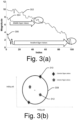
- Fig. 3(a) illustrates the complete range of Eigen vectors that can be extracted by using a combination of the Arnoldi iteration and the QZ methods described above, in accordance with an implementation of the present subject matter.
- the graph 302 represents the entire Eigen spectrum.
- the medium magnitude Eigen values, also referred to as interior Eigen values, are represented by the graph 304.
- the Eigen vectors corresponding to the interior Eigen values can be extracted using the Arnoldi iteration.
- the small magnitude Eigen values are represented by the graph 306.
- the Eigen vectors corresponding to the small magnitude Eigen values can be extracted using the QZ method.
- Fig. 3(b) illustrates the terminal and interior Eigen values in an Eigen spectrum in a complex plane, in accordance with an implementation of the present subject matter.
- the Eigen spectrum is in the shape of a disc 308 in the complex plane.
- the terminal Eigen values are the Eigen values that lie on the perimeter of the disc 308, such as the Eigen value 310.
- the interior Eigen values are the ones that lie anywhere between the centre of the disc 308 and the perimeter of the disc 308, such as the Eigen value 312.
- the Eigen values upon extraction of the Eigen vectors corresponding to the terminal and interior Eigen values, the Eigen values can be sorted based on their magnitude. Thereafter, the Eigen vectors whose corresponding Eigen values are small or medium are selected for augmenting the Krylov subspace.
- the selection of the small and medium Eigen vectors can be performed based on the number of small and medium Eigen vectors to be used for the augmentation. For example, if 50 small Eigen vectors are to be utilized, the Eigen vectors corresponding to the smallest 50 Eigen values are selected. Similarly, if 50 middle Eigen vectors are to be selected, the Eigen vectors corresponding to the smallest 50 interior Eigen values (Eigen values lying between the centre and the perimeter of the disc 308) can be selected.
- small Eigen vectors refers to Eigen vectors corresponding to a predetermined number of the smallest Eigen values amongst the determined Eigen values.
- large Eigen vectors refers to Eigen vectors corresponding to a predetermined number of the largest Eigen values amongst the determined Eigen values.
- Medium Eigen vectors refers to Eigen vectors corresponding to a predetermined number of the smallest interior Eigen values amongst the determined interior Eigen values.
- the predetermined number of Eigen values (50 in the above example) to be used, in turn, can be determined based on the desired speed-up in the solving.
- a combination of Eigen vectors selected from the ranges 304 and 306 may be used to augment the Krylov subspace of the earlier solved EM structure, such as the first EM structure 102. Such a method can fully extract the advantage of both small terminal and interior Eigen vectors from the original EM structure.
- Fig. 3(c) illustrates the convergence speed-up obtained upon using Eigen vectors corresponding to small, medium, and large Eigen values, in accordance with an implementation of the present subject matter.
- the Eigen vectors corresponding to small Eigen values (illustrated by graph 314), and the Eigen vectors corresponding to medium Eigen values (illustrated by graph 316) are more effective in speeding-up the iterative convergence, while the Eigen vectors corresponding to large Eigen values (illustrated by graph 318) do not enable faster iterative convergence.
- Figs. 4(a) and 4(b) illustrate a case in which, while the geometrical properties of the EM structures 102 and 104 are similar, the mesh structure M1 of the first EM structure 102 is significantly different from the mesh structure M2 of the second EM structure 104. Therefore, any Eigen vector data used from the simulation of the first EM structure 102 in the simulation on the second EM structure 104 would not aid in faster convergence of the GMRES process.
- the present subject matter utilizes a mesh interpolation technique.
- the mesh interpolation technique enables using EA-GMRES in cases where the mesh structure of the design variant is different from the already EM modelled and simulated EM structure.
- Figs. 5(a) and 5(b) illustrate the mesh interpolation technique, in accordance with an implementation of the present subject matter.
- M3 represents a third mesh structure for a third EM structure 502
- M4 represents a fourth, different mesh structure for a fourth EM structure 504 that is a design variant of the third EM structure 502.
- the third EM structure 502 is already EM modelled and simulated, similar to the first EM structure 102
- the fourth EM structure 504 is a design variant of the third EM structure 502 and yet to be EM modelled and simulated, similar to the second EM structure 104.
- the third and fourth EM structures have different mesh structures.
- the mesh current matrix for M4 can be reframed in terms of the mesh current matrix for M3 through a linear transformation 506.
- a tree structure is generated by encompassing the entire geometry of the third EM structure 502 inside a cube 507 followed by recursive splitting of each cube into eight children cubes until an optimal number of levels are reached, as would be understood by a person skilled in the art.
- This is called an oct-tree decomposition.
- a level that is not further split is called the leaf level.
- the leaf level cubes corresponding to this multilevel oct-tree-based hierarchical decomposition of the third EM structure 502 are used for the mesh interpolation.
- An oct-tree decomposition is also performed for the fourth EM structure 504 using the cube 507 to obtain the current matrix M4.
- the current vectors of M3 are then transformed into current vectors of M4 by interpolation.
- Fig. 5(c) illustrates a method 512 for mesh interpolation, in accordance with an implementation of the present subject matter.
- the method 512 may be implemented by processor(s) or computing device(s) through any suitable hardware including embedded hardware, FPGA, array of micro-controllers, non-transitory machine readable instructions, or a combination thereof.
- steps of the method 512 may be performed by programmed computing devices and may be executed based on instructions stored in a non-transitory computer readable medium.
- the non-transitory computer readable medium may include, for example, digital memories, magnetic storage media, such as one or more magnetic disks and magnetic tapes, hard drives, or optically readable digital data storage media.
- each edge centre 508 in the mesh structure M4 of the fourth EM structure 504 is mapped to a corresponding mesh component in the mesh structure M3 of the third EM structure 502.
- a set of linear transformations 506 is applied to generate interpolated Krylov vectors.
- the linear transformation 506 can be performed by mapping edge centres within a leaf level cube in M4 with corresponding mesh components on M3. For example, an edge centre 508 in M4 may be mapped on to triangle 510 in M3. The mapping can be performed as below.
- J ⁇ S M 3 1 2
- a M 3 ⁇ n 1 Nb C n M 3 ⁇ ⁇ n M 3 l n M 3
- n takes the contribution over all RWG basis (Nb) functions associated with a triangle of M3 with area A M3 on which the edge-centre of M4 is mapped.
- LHS Left Hand Side
- i is the index of an RWG edge for mesh M4
- M is the number of RWG edges in M4
- the dot product signifies the component of Js normal to the edge.
- the interpolation technique is dependent on the type of Basis function used.
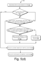
- Fig. 5(d) illustrates a method 550 of mesh interpolation, in accordance with an implementation of the present subject matter.
- the method 550 may be implemented by processor(s) or computing device(s) through any suitable hardware including embedded hardware, FPGA, array of micro-controllers, non-transitory machine readable instructions, or a combination thereof.
- steps of the method 550 may be performed by programmed computing devices and may be executed based on instructions stored in a non-transitory computer readable medium.
- the non-transitory computer readable medium may include, for example, digital memories, magnetic storage media, such as one or more magnetic disks and magnetic tapes, hard drives, or optically readable digital data storage media.
- the fourth EM structure 504, also referred to as D4 is encompassed in the cube hierarchy 507 of the third EM structure 502, referred to as D3, as illustrated in Fig. 5(b) .
- a check is made as to whether all leaf-level cubes of D4 are considered. If not considered, at block 556, for a leaf-level cube that is not considered, a check is made as to whether all edge centres within each leaf-level cube is considered.
- edge centre of M4 in a leaf level cube not considered a determination is made as to whether the edge centre lies within the cube in M3.
- An edge centre of M4 may not lie within the cube in M3 if D4 is an extended version of the D3 and the edge centre lies in a portion of D4 that is absent in D3.
- the edge centre lies within a triangle in M3, at block 560, the edge-centre is mapped to the appropriate triangle in M3, such as the mapping of the edge centre 508 with the triangle 510. If the edge centre of M4 falls outside the cube in M3, at block 562, zero-padding is performed for that edge centre. In general, if it is determined that the edge centre does not have a corresponding mesh component in the first EM structure, a zero padding is provided for that edge centre.
- the above steps of the mesh interpolation technique may be performed by a simulator system as matrix operations in a computational environment.
- m and n represent the number of RWG basis functions for M4 on D4 and M3 on D3 respectively.
- I N represents the coefficients of RWG bases for D3 after explicit MoM solution
- I M represents the interpolated coefficients of RWG basis for D4 obtained by the mesh interpolation process from I N
- T x to be the x th triangle on mesh M3 of base design D3 with an area A x .
- R i be the i th RWG edge on mesh M4 with edge-normal unit vector n i
- R j be the j th RWG edge of length l j on mesh M3.
- the mesh interpolation technique as described above can be used to interpolate Krylov vectors.
- the Krylov vectors of D3 can be used to generate approximate Krylov vectors for D4 using the mesh interpolation technique.
- the interpolated Krylov vectors can be used to generate interpolated Eigen vectors for augmentation to a Krylov subspace of D4. The generation of interpolated Eigen vectors from the interpolated Krylov vectors will be explained later.
- Fig. 5(e) illustrates a comparison of magnitude of the mesh interpolated Krylov vectors with actual Krylov vectors, in accordance with an implementation of the present subject matter.
- the mesh interpolation technique is performed for the Krylov vectors of the first EM structure 102 to obtain mesh interpolated Krylov vectors for the second EM structure 104. They are then compared with the actual Krylov vectors of the second EM structure 104 which are independently computed from Krylov subspace. As can be seen, the mesh interpolated Krylov vectors closely resemble the ones independently generated. Therefore, the mesh interpolation will aid in convergence faster when used for solving the second EM structure 104.
- Figs. 6(a) and 6(b) illustrate applications of mesh interpolation, in accordance with an implementation of the present subject matter.
- a GHz port meander track line in a printed circuit board (PCB) is considered for mesh interpolation with different mesh structures M5 and M6 in Fig. 6(a) and Fig. 6(b) , respectively.
- the MoM system matrix corresponding to M5 is first solved using a regular fast iterative GMRES solution.
- the mesh count of M5 is then increased by 30% to get a new mesh M6.
- the current density obtained from the solution of M5 is next interpolated using (20) and (21) to obtain the coefficients of RWG basis on M6.
- the mesh interpolation technique can be used for compensating for the change in the mesh structures, as described above, and then EA-GMRES can be performed to ensure a faster solution of the design variant.
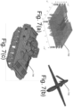
- Figs. 7(a), 7(b), and 7(c) illustrate some EM structures that can be subjected to EM modelling using techniques of the present subject matter, in accordance with some implementations of the present subject matter.
- Fig. 7(a) illustrates triangular meshing on the surface of an electronic packaging structure 702 that can be EM modelled. Using techniques of the present subject matter, the electronic packaging structure 702 can be EM modelled and simulated to ensure EMC and a minimal EMI.
- Fig. 7(b) illustrates triangular meshing on the surface of an aerial vehicle 704 that can be EM modelled.
- Fig. 7(c) illustrates triangular meshing on the surface of a terrestrial vehicle 706 that can be EM modelled. Using techniques of the present subject matter, the aerial vehicle 704 and the terrestrial vehicle 706 can be EM modelled can be EM modelled. Using techniques of the present subject matter, the aerial vehicle 704 and the terrestrial vehicle 706 can be EM modelled and simulated to ensure their
- the methods of the present subject matter speed up solving of the mesh equations considering that each of these illustrated EM structures are design variants of previously solved EM structures that may be smaller in geometric sizing and modified shapes on the surface contours.
- the steps involved in the mesh interpolation technique explained with reference to Figs. 5(a), 5(b) , 5(c) , 5(d) and equation (22) can be used to interpolate the Krylov vectors.
- the Krylov subspace of the second EM structure is augmented with the interpolated Krylov vectors to form an augmented Krylov subspace.
- the Maxwell's equations for the second EM structure are solved using this augmented Krylov subspace.
- the solution of the Maxwell's equations can be performed using the GMRES method, as briefly explained above.
- Such a method of augmenting the Krylov subspace of the second EM structure and using this augmented Krylov subspace for solving Maxwell's equations may be referred to as mesh interpolated Krylov Recycling (MIKR) method.
- MIKR mesh interpolated Krylov Recycling
- Fig. 8 illustrates a schematic flow of the MIKR method, in accordance with an implementation of the present subject matter.
- the MIKR methodology can be applied to obtain the solution of a design variant D2, such as the second EM structure 104, of another EM structure D1, such as the first EM structure 102, as explained above.
- the mesh-interpolated Krylov vectors are re-orthogonalized (transformed into a new equivalent set of mutually perpendicular vectors in the N dimensional subspace using methods similar to the Gram-Schmidt process known in art) and augmented in the Krylov subspace of D2 for solving the Maxwell's equations using GMRES solution.
- the augmentation of the Krylov subspace as performed in the MIKR method provides a faster solving of D2.
- the faster solving is illustrated with the help of another EM structure in Fig. 9(a) and Fig. 9(b) .
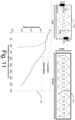
- Figs. 9(a), 9(b) , and 9(c) illustrate faster convergence in the solving of an extended EM structure due to the MIKR method, in accordance with an implementation of the present subject matter.
- Fig. 9(a) illustrates a first via (an electrical connection between layers in a physical electronic circuit that goes through an insulating layer plane between one or more adjacent layers) structure of the circuit plane 902 over ground plane that is considered in a GHz PCB routing design.
- Fig. 9(b) illustrates a second via structure circuit plane 904 that is a design variant of the first via structure circuit plane 902.
- the second via structure circuit plane 904 includes two vias 906 and 908, as opposed to a single via 910 of the first via structure 902. Therefore, the second via structure 904 can be considered as an extended EM structure.
- Table - I shows the physical dimensions of layout used in this example. TABLE I.
- the second via structure 904 is simulated using the proposed MIKR solver for all frequency points with lumped port as excitation.
- Fig. 9(d) illustrates comparison of results obtained using MIKR-GMRES and results obtained using a conventional GMRES performed by a commercial tool, in accordance with an implementation of the present subject matter.
- MIKR-GMRES refers to performing a GMRES operation after augmenting the Krylov subspace of the second via structure 904 with interpolated Krylov vectors of the first via structure 902.
- MIKR-GMRES method refers to performing a GMRES operation after augmenting the Krylov subspace of D2 with interpolated Krylov vectors of D1.
- the MIKR-GMRES method of the present subject matter is as accurate as the solution set obtained using a conventional GMRES and the solution is reached in substantially lesser number of iterative steps.
- Fig. 10 illustrates a 3 ⁇ 3 dielectric voxel structure 1000 for which the simulation is accelerated using the MIKR method and using the Krylov subspace of a primary voxel structure (one of the nine shown in Fig. 10 ) whose solution is known, in accordance with an implementation of the present subject matter (Voxel represents a volumetric mesh element that is used to discretize dielectric structures just as triangles are used to discretize the surface of conductor structure).
- each voxel is considered to have the same dielectric constant ( ⁇ r ) equal to three.
- the middle voxel dielectric constant is changed to six keeping the dielectric constant of other voxels fixed at three.
- a simulation frequency of 4.5 GHz is chosen for the application.
- the structure is excited from the top with negative z-directed linearly polarized E-field plane wave with 1 V/m strength.
- the savings in the simulation of the design variant using MIKR methodology as compared to regular GMRES is presented in Table III, where p represents the number of matrix-vector products required for convergence. It can be observed from Table III that MIKR achieves a speed-up of ⁇ 5x.
- Fig. 11 illustrates another practical application design where a Meander line in a GHz port PCB design is extended and is to be solved as a design variant, in accordance with an implementation of the present subject matter.
- Meander line structures are used in delay line applications as in Double Data Rate 3 (DDR3), DDR4 random access memories (RAMs) designs which require perfect delays to synchronize with a system clock.
- DDR3 Double Data Rate 3
- RAMs DDR4 random access memories
- a first meander line 1102 with 4.5 turns over FR4 dielectric on a PCB is considered as the base design.
- a second meander line 1104 having 8 turns is used as a design variant. Both structures are simulated at 20 GHz with lumped port excitation.
- the convergence profile of the GMRES process is illustrated for the design variant in graph 1106 with Full GMRES and MIKR-GMRES.
- the performance metrics are tabulated in Table IV. As shown in Table IV, a speed-up of around ⁇ 3x is achieved using MIKR. TABLE IV PERFORMANCE OF MIKR-GMRES COMPARED TO FULL-GMRES FOR MEANDER-LINE STRUCTURE Design variant Change in properties Number of RWG edges Full GMRES (p) MIKR-GMRES (p) D1 : Base Design Meander Line with 4.5 turns 23821 138 - D2 Meander Line with 8 turns 5210 437 137
- Fig. 12 illustrates preservation of solution accuracy when using the MIKR procedure for the meander line implementation of Fig. 11 , in accordance with an implementation of the present subject matter.
- the Z-parameter results for the MIKR procedure are compared to a full GMRES simulation.
- the solution accuracy is preserved when the MIKR procedure.
- MIKR-GMRES method detailed out as in the paragraphs above is for reusing information from the solution of a base design to expedite the convergence of a design variant.
- the method is independent of the choice of fast-solver scheme and the preconditioning technique.
- Numerical results demonstrate a speed-up of 2-5 x as compared to a regular fast-solver based GMRES procedure.
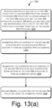
- Fig. 13(a) illustrates a method 1300 for EM modelling of an EM structure using Krylov subspace augmented with Krylov vectors and Eigen vectors, in accordance with an implementation of the present subject matter.
- the method 1300 may be implemented by processor(s) or computing device(s) through any suitable hardware, non-transitory machine readable instructions, or a combination thereof.
- steps of the method 1300 may be performed by programmed computing devices and may be executed based on instructions stored in a non-transitory computer readable medium.
- the non-transitory computer readable medium may include, for example, digital memories, magnetic storage media, such as one or more magnetic disks and magnetic tapes, hard drives, or optically readable digital data storage media.
- Krylov vectors of a first EM structure are interpolated to a second EM structure, where the second EM structure is a design variant of the first EM structure, the first EM structure is already EM modelled and simulated, and mesh structure of the first EM structure is different from that of the second EM structure.
- the first EM structure can be, for example, the first EM structure 102 and the second EM structure can be, for example, the second EM structure 104.
- the interpolation of the Krylov vectors can be performed using the mesh interpolation technique described with reference to Figs. 5(a), (b), (c), and (d) .
- a Krylov subspace of the second EM structure is augmented with the interpolated Krylov vectors to form an augmented Krylov subspace.
- the augmented Krylov subspace of the second EM structure is augmented with interpolated Eigen vectors of the first EM structure to form an augmented space.
- the Maxwell's equations for the second EM structure are solved using the augmented space.
- Fig. 13(b) illustrates the KREAM method 1350, in accordance with an implementation of the present subject matter.
- the method 1350 may be implemented by processor(s) or computing device(s) through any suitable hardware, non-transitory machine readable instructions, or a combination thereof.
- steps of the method 1350 may be performed by programmed computing devices and may be executed based on instructions stored in a non-transitory computer readable medium.
- the non-transitory computer readable medium may include, for example, digital memories, magnetic storage media, such as one or more magnetic disks and magnetic tapes, hard drives, or optically readable digital data storage media.
- D1 and D2 are the two near-identical design variants, such as the first EM structure 102 and the second EM structure 104, with arbitrary number of Mesh elements.
- N1 and N2 are the number of RWG edges for systems D1 and D2 and these are represented by the matrices Z MoM (D1) and Z MoM (D2), respectively.
- the matrix for D1, Z MoM (D1) is solved by the GMRES method, as known in the art and briefly explained above.
- a Hessenberg matrix (H pxp ) is obtained.
- the Hessenberg matrix may be obtained using modified Arnoldi method of orthogonalization, as known in the art.
- p is the number of iterations to converge.
- the approximate Eigen vectors (E1 N1xe1 ) of Z MoM (D1) are selected and saved as Eigen space from the Hessenberg matrix corresponding to Eigen values of smallest magnitude and interior Eigen vectors.
- Eigen vectors having corresponding small and medium magnitude Eigen values are selected and saved as the Eigen space.
- e1 refers to the number of eigen vectors saved.
- the Eigen vectors corresponding to Eigen values of smallest magnitude can be selected using the QZ method.
- the interior eigen vectors can be selected using the Harmonic Arnoldi method.
- the Krylov subspace (K r1 ) of D1 is selected and mesh interpolated to the size of D2.
- the mesh interpolation can be performed using the procedure explained with reference to Figs. 5(a), (b), and (c) .
- the mesh interpolated Krylov subspace is stored as K r1_ interp N2xp1 , where p1 is the number of iterations to converge.
- an augmented GMRES is performed for D2 with the augmented space to arrive at the solution for D2, i.e., to solve the Maxwell's equations for D2.
- the augmented GMRES is explained with reference to Fig. 14 .
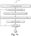
- Fig. 14 illustrates the augmented GMRES, in accordance with an implementation of the present subject matter.
- the method 1400 may be implemented by processor(s) or computing device(s) through any suitable hardware, non-transitory machine readable instructions, or a combination thereof.
- steps of the method 1400 may be performed by programmed computing devices and may be executed based on instructions stored in a non-transitory computer readable medium.
- the non-transitory computer readable medium may include, for example, digital memories, magnetic storage media, such as one or more magnetic disks and magnetic tapes, hard drives, or optically readable digital data storage media.
- V p ⁇ R n ⁇ p has orthonormal columns and R ⁇ R p ⁇ n is upper triangular.
- Z MoM (D2) * K r1_ interp N2xp1 and Z MoM (D2) * E 1_ interp N2xe1 come from mesh interpolating Z MoM (D2) * K r1_ interp N2xp1 and Z MoM (D2) * E 1_ interp N2xe1 to the system size of N2 of D2.
- the current Krylov subspace may be generated by the modified Arnoldi method, as explained earlier.
- the first column of the trailing n ⁇ ( j +1) sub-matrix V p+1:p+j+1 of V p+j+1 is I ⁇ V p V p T b / ⁇ I ⁇ V p V p T b ⁇ for augmented GMRES.
- the leading principal p ⁇ p submatrix of the upper Hessenberg matrix H ⁇ R (p+j+1) ⁇ (p+j) is upper triangular matrix R in QR factorization.
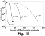
- Fig. 15 illustrates the results of application of the KREAM method for an incremental design problem, in accordance with an implementation of the present subject matter.
- Full GMRES is compared with MIKR-GMRES and KREAM.
- the augmentation of KREAM is developed by restoring interpolated Krylov subspace and adding middle and smallest Eigen vectors to the augmentation space.
- graph 1502 represents the results from full GMRES
- 1504 represents results from MIKR-GMRES
- 1506 represents results from adding smallest Eigen vectors to the augmentation space
- 1508 represents results from adding middle Eigen vectors to the augmentation space. It can be seen that the KREAM method provided much faster convergence compares to full GMRES and MIKR-GMRES. It can also be seen that with middle Eigen vectors, simulator speed up between 10 ⁇ and 20 ⁇ can be achieved.
- FIGs. 16(a) and 16(b) illustrate the use of a KREAM method based simulator, in accordance with an implementation of the present subject matter.
- 1602 represents a basic EM structure that is already solved
- 1604 represents an extended EM structure, extended over the basic EM structure 1602.
- the EM structures 1602 and 1604 relate to an Inverted-F Antenna over air substrate.
- the EM structure is simulated from 10 GHz to 13 GHz with increment of 500 MHz.
- the incremental problem is created at 12 GHz with second design variant as elongated length of antenna arm as in 1604 in Fig. 16(a) and with higher mesh density.
- antenna is tuned by setting the arm length as parameter in order to match the feed impedance for better standing wave ratio.
- Table VI below exemplifies the physical dimensions of the layout.
- Table VI Physical dimensions of layout for Fig. 14 Physical Parameter Description value L1 Initial trace length 1 mm L Pad diameter 2 mm X Post pad trace length 1 mm ⁇ L Via diameter 1 mm
- Fig. 17 illustrates a computational system 1700 for EM modelling of an EM structure, in accordance with an implementation of the present subject matter.
- the computational system 1700 can be used to perform any of the above described methods for speeding-up solving of EM structures.
- the computational system 1700 includes a processor(s) 1702, interface(s) 1704, memory 1706, electromagnetic (EM) modelling module 1708, other module(s) 1710, and system data 1712.
- the computational system 1700 may be implemented as any computing system which may be, but is not restricted to, a server, a workstation, a desktop computer, a laptop, a smartphone, a personal digital assistant (PDA), a tablet, a virtual host, and an application.
- the computational system 1700 may also be machine-readable instructions based implementation or a hardware-based implementation, or a combination thereof.
- the processor(s) 1702 may be implemented as microprocessors, microcomputers, microcontrollers, digital signal processors, central processing units, state machines, logic circuitries, and/or any devices that manipulate signals based on operational instructions. Among other capabilities, the processor(s) 1702 may fetch and execute computer-readable instructions stored in a memory. The functions of the processor(s) 1702 may be provided through the use of dedicated hardware as well as hardware capable of executing machine readable instructions.
- processor(s) system 1702 and the memory may be integrated into one processor chip with multiple cores and the on chip memory directly divided and bus connectable to multiple clusters of the processor(s) cores to aid rapid parallelization of the iterative procedures involved in the matrix solution with the Augmented Krylov space method with mesh interpolation.
- the interface(s) 1704 may include a variety of machine readable instructions-based interfaces and hardware interfaces that allow interaction with a user and with other communication and computing devices, such as network entities, web servers, and external repositories, and peripheral devices.
- the memory 1706 may be coupled to the processor(s) 1702 and may, among other capabilities, provide data and instructions for generating different requests.
- the memory 1706 can include any computer readable medium known in the art including, for example, volatile memory, such as static random access memory (SRAM) and dynamic random access memory (DRAM), Multi-channel DRAM (MCDRAM) and/or nonvolatile memory, such as read only memory (ROM), erasable programmable ROM, flash memories, hard disks, optical disks, and magnetic tapes.
- volatile memory such as static random access memory (SRAM) and dynamic random access memory (DRAM), Multi-channel DRAM (MCDRAM) and/or nonvolatile memory, such as read only memory (ROM), erasable programmable ROM, flash memories, hard disks, optical disks, and magnetic tapes.
- SRAM static random access memory
- DRAM dynamic random access memory
- MCDRAM Multi-channel DRAM
- nonvolatile memory such as read only memory (ROM), erasable programmable
- the EM modelling module 1708, and the other modules 1710 may be coupled to and/or be executable by processor(s), and may include, amongst other things, routines, programs, objects, components, data structures, and the like, which perform particular tasks or implement particular abstract data types.
- the other modules 1710 may include programs or coded instructions that supplement applications and functions, for example, programs in the operating system, of the computational system 1700.
- the EM modelling module 1708 and the other modules 1710 may be implemented as a part of the same module. Further, the EM modelling module 1708 and the other modules 1710 may be implemented in hardware, instructions executed by a processing unit, or by a combination thereof.
- the system data 1712 may serve as a repository for storing data that may be fetched, processed, received, or created by the EM modelling module 1708 during the iterative simulation procedure and the other modules 1710 or received from connected computing systems and storage devices.
- the EM modelling module 1708 can augment Krylov subspace of a second EM structure with Eigen vectors of a first EM structure to form an augmented space, where the second EM structure is a design variant of the first EM structure and the first EM structure is already EM modelled and simulated. Further, the EM modelling module 1708 can then solve Maxwell's equations for the second EM structure using the augmented space.
- the EM modelling module 1708 can interpolate Krylov vectors of a first EM structure, augment Krylov subspace of the second EM structure with the interpolated Krylov vectors to form an augmented Krylov subspace, augment the augmented Krylov subspace of the second EM structure with interpolated Eigen vectors of the first EM structure to form an augmented space, and solve Maxwell's equations for the second EM structure using the augmented Krylov subspace.
Landscapes
- Engineering & Computer Science (AREA)
- Physics & Mathematics (AREA)
- Theoretical Computer Science (AREA)
- General Physics & Mathematics (AREA)
- Mathematical Physics (AREA)
- Geometry (AREA)
- General Engineering & Computer Science (AREA)
- Software Systems (AREA)
- Computational Mathematics (AREA)
- Mathematical Analysis (AREA)
- Mathematical Optimization (AREA)
- Pure & Applied Mathematics (AREA)
- Data Mining & Analysis (AREA)
- Evolutionary Computation (AREA)
- Computer Hardware Design (AREA)
- Computer Graphics (AREA)
- Computing Systems (AREA)
- Algebra (AREA)
- Databases & Information Systems (AREA)
- Complex Calculations (AREA)
- Management, Administration, Business Operations System, And Electronic Commerce (AREA)
Claims (9)
- Computerimplementiertes Verfahren (200) zur elektromagnetischen, EM, Modellierung und Simulation einer EM-Struktur, wobei die EM-Struktur eine elektronische Verpackungsstruktur ist, um die elektromagnetische Kompatibilität zu gewährleisten und die elektromagnetische Interferenz der EM-Struktur zu reduzieren, wobei das Verfahren umfasst:Erhalten von Eigenvektoren einer ersten EM-Struktur aus der Lösung der Maxwell-Gleichungen für die erste EM-Struktur, wobei die Maxwell-Gleichungen für die erste EM-Struktur (102, 502) während der EM-Modellierung und Simulation der ersten EM-Struktur gelöst werden;dadurch gekennzeichnet, dass das Verfahren umfasst:wenn eine Maschenstruktur (M1, M3) der ersten EM-Struktur (102, 502) sich von derjenigen (M2, M4) einer zweiten EM-Struktur (104, 504) unterscheidet, Interpolieren der Eigenvektoren der ersten EM-Struktur (102, 502) zu einer zweiten EM-Struktur (104, 504), wobei die zweite EM-Struktur (104, 504) eine Designvariante der ersten EM-Struktur (102, 502) ist;Auswählen von Eigenvektoren der ersten EM-Struktur (102, 502), die in den Krylov-Unterraum der zweiten EM-Struktur (104, 504) zu augmentieren sind, wobei jeder Eigenvektor einen entsprechenden Eigenwert hat, wobei jeder Eigenwert einen von einer kleinen, mittleren und großen Größe hat, und wobei das Auswählen von Eigenvektoren das Auswählen eines Eigenvektors in Reaktion auf einen Eigenwert umfasst, der dem Eigenvektor mit einer kleinen Größe oder einer mittleren Größe entspricht, wobei der Eigenwert mit mittlerer Größe einer vorbestimmten Anzahl der kleinsten inneren Eigenwerte entspricht, der Eigenwert mit kleiner Größe einer vorbestimmten Anzahl der kleinsten terminalen Eigenwerte entspricht, der Eigenwert mit großer Größe einer vorbestimmten Anzahl der größten terminalen Eigenwerte entspricht;Erweitern des Krylov-Unterraums der zweiten EM-Struktur (104, 504) mit den ausgewählten Eigenvektoren, um einen erweiterten Raum zu bilden; undLösen der Maxwell-Gleichungen für die zweite EM-Struktur (104, 504) unter Verwendung des erweiterten Raums, um EM-Modellierung und -Simulation der zweiten EM-Struktur durchzuführen, wobei das Lösen der Maxwell-Gleichungen verwendet wird, um die elektromagnetische Kompatibilität der zweiten EM-Struktur zu ermitteln.
- Verfahren nach Anspruch 1, wobei das Interpolieren der Eigenvektoren der ersten EM-Struktur (102, 502) in die zweite EM-Struktur (104, 504) umfasst:Interpolieren von Krylov-Vektoren der ersten EM-Struktur (102, 502) in die zweite EM-Struktur (104, 504); undErzeugung von interpolierten Eigenvektoren auf der Grundlage von interpolierten Krylov-Vektoren.
- Verfahren nach Anspruch 2, wobei das Interpolieren der Krylov-Vektoren umfasst:Abbilden jedes Kantenzentrums (508) in der Maschenstruktur (M2, M4) der zweiten EM-Struktur (104, 504) auf eine entsprechende Maschenkomponente (210) in der Maschenstruktur (M1, M3) der ersten EM-Struktur (102, 502); undAnwendung einer Reihe von linearen Transformationen (506) zur Erzeugung der interpolierten Krylov-Vektoren.
- Verfahren nach Anspruch 1, wobei die zweite EM-Struktur (104, 504) eine größere oder kleinere Abmessung als die erste EM-Struktur (102, 502) aufweist.
- Verfahren nach Anspruch 1, wobei die Maxwell-Gleichungen für die zweite EM-Struktur (104, 504) unter Verwendung eines Generalized Minimal Residual ,GMRES, Prozesses in dem erweiterten Raum gelöst werden.
- Verfahren nach Anspruch 2, umfassend:
Erweiterung des Krylov-Unterraums der zweiten EM-Struktur (104, 504) mit den interpolierten Krylov-Vektoren vor der Lösung der Maxwellschen Gleichungen für die zweite EM-Struktur. - System (1700) zum Durchführen einer elektromagnetischen, EM, Modellierung und Simulation einer EM-Struktur (104, 504), wobei die EM-Struktur eine elektronische Gehäusestruktur ist, um elektromagnetische Kompatibilität sicherzustellen und elektromagnetische Interferenz zu reduzieren, wobei das System (1700) umfasst:einen Prozessor (1702);ein EM-Modellierungsmodul (1708), das mit dem Prozessor (1702) verbunden ist, um:Eigenvektoren einer ersten EM-Struktur aus der Lösung der Maxwell-Gleichungen für die erste EM-Struktur zu erhalten, wobei die Maxwell-Gleichungen für die erste EM-Struktur (102, 502) während der EM-Modellierung und Simulation der ersten EM-Struktur gelöst werden;dadurch gekennzeichnet ist, dass das EM-Modellierungsmodul dazu ausgebildet ist,wenn eine Maschenstruktur (M1, M3) der ersten EM-Struktur (102, 502) sich von derjenigen (M2, M4) der zweiten EM-Struktur (104, 504) unterscheidet, interpolieren der Eigenvektoren der ersten EM-Struktur (102, 502) in die zweite EM-Struktur, wobei die zweite EM-Struktur (104, 504) eine Designvariante der ersten EM-Struktur (102, 502) ist;Auswählen von Eigenvektoren der ersten EM-Struktur (102, 502), die im Krylov-Unterraum der zweiten EM-Struktur (104, 504) zu augmentieren sind, wobei jeder Eigenvektor einen entsprechenden Eigenwert hat, wobei jeder Eigenwert einen von einem kleinen, mittleren und großen Betrag hat, und wobei zum Auswählen der Eigenvektoren das EM-Modellierungsmodul einen Eigenvektor als Reaktion auf einen Eigenwert auswählen soll, der dem Eigenvektor mit einem kleinen Betrag oder einem mittleren Betrag entspricht, wobei der Eigenwert mit mittlerer Größe einer vorbestimmten Anzahl der kleinsten inneren Eigenwerte entspricht, der Eigenwert mit kleiner Größe einer vorbestimmten Anzahl der kleinsten terminalen Eigenwerte entspricht, der Eigenwert mit großer Größe einer vorbestimmten Anzahl der größten terminalen Eigenwerte entspricht;Erweitern des Krylov-Unterraums der zweiten EM-Struktur (104, 504) mit den ausgewählten Eigenvektoren der ersten EM-Struktur, um einen erweiterten Unterraum zu bilden;die Maxwell-Gleichungen für die zweite EM-Struktur (104, 504) unter Verwendung des erweiterten Raums zu lösen, um eine EM-Modellierung und -Simulation der zweiten EM-Struktur durchzuführen, wobei das Lösen der Maxwell-Gleichungen dazu dient, die elektromagnetische Verträglichkeit der zweiten EM-Struktur zu ermitteln.
- System (1700) nach Anspruch 7, wobei das EM-Modellierungsmodul zur Interpolation der Eigenvektoren der ersten EM-Struktur (102, 502) in die zweite EM-Struktur (104, 504) zufolgedem dient:Interpolieren von Krylov-Vektoren der ersten EM-Struktur (102, 502) in die zweite EM-Struktur (104, 504); und Erzeugeninterpolierter Eigenvektoren auf der Grundlage der interpolierten Krylov-Vektoren.
- System (1700) nach Anspruch 8, wobei zur Interpolation der Krylov-Vektoren das EM-Modellierungsmodul (1708) dazu dient:jedes Kantenzentrum (508) in der Maschenstruktur (M2, M4) der zweiten EM-Struktur (104, 504) auf eine entsprechende Maschenkomponente (210) in der Maschenstruktur (M1, M3) der ersten EM-Struktur (102, 502) abzubilden; undeine Reihe von linearen Transformationen (506) anwenden, um die interpolierten Krylov-Vektoren zu erzeugen.
Applications Claiming Priority (2)
| Application Number | Priority Date | Filing Date | Title |
|---|---|---|---|
| IN201641024555 | 2016-07-18 | ||
| PCT/IN2017/050295 WO2018015972A1 (en) | 2016-07-18 | 2017-07-18 | Eigen augmentation methods for electromagnetic modelling and simulation |
Publications (2)
| Publication Number | Publication Date |
|---|---|
| EP3485404A1 EP3485404A1 (de) | 2019-05-22 |
| EP3485404B1 true EP3485404B1 (de) | 2023-11-01 |
Family
ID=59791105
Family Applications (1)
| Application Number | Title | Priority Date | Filing Date |
|---|---|---|---|
| EP17761931.9A Active EP3485404B1 (de) | 2016-07-18 | 2017-07-18 | Methode für elektromagnetische modellierung und simulation mit augmentierten eigenwerten |
Country Status (3)
| Country | Link |
|---|---|
| US (1) | US11244094B2 (de) |
| EP (1) | EP3485404B1 (de) |
| WO (1) | WO2018015972A1 (de) |
Families Citing this family (5)
| Publication number | Priority date | Publication date | Assignee | Title |
|---|---|---|---|---|
| US11461514B2 (en) * | 2018-09-24 | 2022-10-04 | Saudi Arabian Oil Company | Reservoir simulation with pressure solver for non-diagonally dominant indefinite coefficient matrices |
| CN111428407B (zh) * | 2020-03-23 | 2023-07-18 | 杭州电子科技大学 | 一种基于深度学习的电磁散射计算方法 |
| US11734384B2 (en) | 2020-09-28 | 2023-08-22 | International Business Machines Corporation | Determination and use of spectral embeddings of large-scale systems by substructuring |
| CN112836375B (zh) * | 2021-02-07 | 2023-03-03 | 中国人民解放军空军工程大学 | 一种高效目标电磁散射仿真方法 |
| CN119169279B (zh) * | 2024-11-20 | 2025-03-14 | 华东交通大学 | 一种交通图像处理方法、系统、存储介质及计算机 |
Family Cites Families (3)
| Publication number | Priority date | Publication date | Assignee | Title |
|---|---|---|---|---|
| US7853910B1 (en) * | 2007-12-21 | 2010-12-14 | Cadence Design Systems, Inc. | Parasitic effects analysis of circuit structures |
| US9529110B2 (en) | 2008-03-31 | 2016-12-27 | Westerngeco L. L. C. | Constructing a reduced order model of an electromagnetic response in a subterranean structure |
| US8510091B1 (en) | 2010-09-09 | 2013-08-13 | Sas Ip, Inc. | Domain decomposition formulations for simulating electromagnetic fields |
-
2017
- 2017-07-18 EP EP17761931.9A patent/EP3485404B1/de active Active
- 2017-07-18 WO PCT/IN2017/050295 patent/WO2018015972A1/en not_active Ceased
- 2017-07-18 US US16/319,221 patent/US11244094B2/en not_active Expired - Fee Related
Non-Patent Citations (1)
| Title |
|---|
| CHATTERJEE GOURAV ET AL: "Learning-Based Fast Iterative Convergence of 3-D MoM via Eigen-AGMRES Method", IEEE TRANSACTIONS ON ANTENNAS AND PROPAGATION, IEEE SERVICE CENTER, PISCATAWAY, NJ, US, vol. 63, no. 12, 1 December 2015 (2015-12-01), pages 5889 - 5893, XP011592401, ISSN: 0018-926X, [retrieved on 20151125], DOI: 10.1109/TAP.2015.2481478 * |
Also Published As
| Publication number | Publication date |
|---|---|
| WO2018015972A1 (en) | 2018-01-25 |
| US20190236227A1 (en) | 2019-08-01 |
| US11244094B2 (en) | 2022-02-08 |
| EP3485404A1 (de) | 2019-05-22 |
Similar Documents
| Publication | Publication Date | Title |
|---|---|---|
| Tamayo et al. | Multilevel adaptive cross approximation (MLACA) | |
| Sumithra et al. | Review on computational electromagnetics | |
| EP3485404B1 (de) | Methode für elektromagnetische modellierung und simulation mit augmentierten eigenwerten | |
| Lee et al. | Incomplete LU preconditioning for large scale dense complex linear systems from electromagnetic wave scattering problems | |
| Özgün et al. | MATLAB-based finite element programming in electromagnetic modeling | |
| WO2023155683A1 (zh) | 电大多尺度复杂目标的三维电磁场求解方法 | |
| Vipiana et al. | EFIE modeling of high-definition multiscale structures | |
| Volakis et al. | Hybrid finite-element methodologies for antennas and scattering | |
| Ma et al. | A 3-D precise integration time-domain method without the restraints of the Courant-Friedrich-Levy stability condition for the numerical solution of Maxwell's equations | |
| Francavilla et al. | Hierarchical fast MoM solver for the modeling of large multiscale wire-surface structures | |
| Yu et al. | Enhanced QMM-BEM solver for three-dimensional multiple-dielectric capacitance extraction within the finite domain | |
| Wu et al. | MLACE-MLFMA combined with reduced basis method for efficient wideband electromagnetic scattering from metallic targets | |
| Zhou et al. | Direct finite-element solver of linear complexity for large-scale 3-D electromagnetic analysis and circuit extraction | |
| Takrimi et al. | A novel broadband multilevel fast multipole algorithm with incomplete-leaf tree structures for multiscale electromagnetic problems | |
| Li et al. | A doubly hierarchical MoM for high-fidelity modeling of multiscale structures | |
| CN114547542A (zh) | 一种三维可控源电磁正演方法及系统 | |
| Cabello et al. | A new conformal FDTD for lossy thin panels | |
| Li et al. | MultiAIM: Fast electromagnetic analysis of multiscale structures using boundary element methods | |
| Li et al. | Out-of-core solver based DDM for solving large airborne array | |
| US7359929B2 (en) | Fast solution of integral equations representing wave propagation | |
| Zhao et al. | A new decomposition solver for complex electromagnetic problems [EM Programmer's Notebook] | |
| Wang | A domain decomposition method for analysis of three-dimensional large-scale electromagnetic compatibility problems | |
| Delgado et al. | An overview of the evolution of method of moments techniques in modern EM simulators | |
| Jiang et al. | SIE-DDM based on a hybrid direct–iterative approach for analysis of multiscale problems | |
| Jiang et al. | Preconditioned MDA-SVD-MLFMA for analysis of multi-scale problems |
Legal Events
| Date | Code | Title | Description |
|---|---|---|---|
| STAA | Information on the status of an ep patent application or granted ep patent |
Free format text: STATUS: UNKNOWN |
|
| STAA | Information on the status of an ep patent application or granted ep patent |
Free format text: STATUS: THE INTERNATIONAL PUBLICATION HAS BEEN MADE |
|
| PUAI | Public reference made under article 153(3) epc to a published international application that has entered the european phase |
Free format text: ORIGINAL CODE: 0009012 |
|
| STAA | Information on the status of an ep patent application or granted ep patent |
Free format text: STATUS: REQUEST FOR EXAMINATION WAS MADE |
|
| 17P | Request for examination filed |
Effective date: 20190213 |
|
| AK | Designated contracting states |
Kind code of ref document: A1 Designated state(s): AL AT BE BG CH CY CZ DE DK EE ES FI FR GB GR HR HU IE IS IT LI LT LU LV MC MK MT NL NO PL PT RO RS SE SI SK SM TR |
|
| AX | Request for extension of the european patent |
Extension state: BA ME |
|
| DAV | Request for validation of the european patent (deleted) | ||
| DAX | Request for extension of the european patent (deleted) | ||
| STAA | Information on the status of an ep patent application or granted ep patent |
Free format text: STATUS: EXAMINATION IS IN PROGRESS |
|
| 17Q | First examination report despatched |
Effective date: 20200818 |
|
| REG | Reference to a national code |
Ref country code: DE Ref legal event code: R079 Free format text: PREVIOUS MAIN CLASS: G06F0017500000 Ipc: G06F0030230000 Ref country code: DE Ref legal event code: R079 Ref document number: 602017076002 Country of ref document: DE Free format text: PREVIOUS MAIN CLASS: G06F0017500000 Ipc: G06F0030230000 |
|
| GRAP | Despatch of communication of intention to grant a patent |
Free format text: ORIGINAL CODE: EPIDOSNIGR1 |
|
| STAA | Information on the status of an ep patent application or granted ep patent |
Free format text: STATUS: GRANT OF PATENT IS INTENDED |
|
| RIC1 | Information provided on ipc code assigned before grant |
Ipc: G06F 111/10 20200101ALN20230417BHEP Ipc: G06F 30/23 20200101AFI20230417BHEP |
|
| INTG | Intention to grant announced |
Effective date: 20230517 |
|
| GRAS | Grant fee paid |
Free format text: ORIGINAL CODE: EPIDOSNIGR3 |
|
| RAP3 | Party data changed (applicant data changed or rights of an application transferred) |
Owner name: BOSCH GLOBAL SOFTWARE TECHNOLOGIES PRIVATE LIMITED Owner name: INDIAN INSTITUTE OF SCIENCE |
|
| GRAA | (expected) grant |
Free format text: ORIGINAL CODE: 0009210 |
|
| STAA | Information on the status of an ep patent application or granted ep patent |
Free format text: STATUS: THE PATENT HAS BEEN GRANTED |
|
| AK | Designated contracting states |
Kind code of ref document: B1 Designated state(s): AL AT BE BG CH CY CZ DE DK EE ES FI FR GB GR HR HU IE IS IT LI LT LU LV MC MK MT NL NO PL PT RO RS SE SI SK SM TR |
|
| REG | Reference to a national code |
Ref country code: GB Ref legal event code: FG4D |
|
| REG | Reference to a national code |
Ref country code: CH Ref legal event code: EP |
|
| REG | Reference to a national code |
Ref country code: DE Ref legal event code: R096 Ref document number: 602017076002 Country of ref document: DE |
|
| REG | Reference to a national code |
Ref country code: IE Ref legal event code: FG4D |
|
| P01 | Opt-out of the competence of the unified patent court (upc) registered |
Effective date: 20240117 |
|
| REG | Reference to a national code |
Ref country code: LT Ref legal event code: MG9D |
|
| REG | Reference to a national code |
Ref country code: NL Ref legal event code: MP Effective date: 20231101 |
|
| PG25 | Lapsed in a contracting state [announced via postgrant information from national office to epo] |
Ref country code: GR Free format text: LAPSE BECAUSE OF FAILURE TO SUBMIT A TRANSLATION OF THE DESCRIPTION OR TO PAY THE FEE WITHIN THE PRESCRIBED TIME-LIMIT Effective date: 20240202 |
|
| PG25 | Lapsed in a contracting state [announced via postgrant information from national office to epo] |
Ref country code: IS Free format text: LAPSE BECAUSE OF FAILURE TO SUBMIT A TRANSLATION OF THE DESCRIPTION OR TO PAY THE FEE WITHIN THE PRESCRIBED TIME-LIMIT Effective date: 20240301 |
|
| PG25 | Lapsed in a contracting state [announced via postgrant information from national office to epo] |
Ref country code: LT Free format text: LAPSE BECAUSE OF FAILURE TO SUBMIT A TRANSLATION OF THE DESCRIPTION OR TO PAY THE FEE WITHIN THE PRESCRIBED TIME-LIMIT Effective date: 20231101 |
|
| REG | Reference to a national code |
Ref country code: AT Ref legal event code: MK05 Ref document number: 1628047 Country of ref document: AT Kind code of ref document: T Effective date: 20231101 |
|
| PG25 | Lapsed in a contracting state [announced via postgrant information from national office to epo] |
Ref country code: NL Free format text: LAPSE BECAUSE OF FAILURE TO SUBMIT A TRANSLATION OF THE DESCRIPTION OR TO PAY THE FEE WITHIN THE PRESCRIBED TIME-LIMIT Effective date: 20231101 |
|
| PG25 | Lapsed in a contracting state [announced via postgrant information from national office to epo] |
Ref country code: AT Free format text: LAPSE BECAUSE OF FAILURE TO SUBMIT A TRANSLATION OF THE DESCRIPTION OR TO PAY THE FEE WITHIN THE PRESCRIBED TIME-LIMIT Effective date: 20231101 |
|
| PG25 | Lapsed in a contracting state [announced via postgrant information from national office to epo] |
Ref country code: ES Free format text: LAPSE BECAUSE OF FAILURE TO SUBMIT A TRANSLATION OF THE DESCRIPTION OR TO PAY THE FEE WITHIN THE PRESCRIBED TIME-LIMIT Effective date: 20231101 |
|
| PG25 | Lapsed in a contracting state [announced via postgrant information from national office to epo] |
Ref country code: NL Free format text: LAPSE BECAUSE OF FAILURE TO SUBMIT A TRANSLATION OF THE DESCRIPTION OR TO PAY THE FEE WITHIN THE PRESCRIBED TIME-LIMIT Effective date: 20231101 Ref country code: LT Free format text: LAPSE BECAUSE OF FAILURE TO SUBMIT A TRANSLATION OF THE DESCRIPTION OR TO PAY THE FEE WITHIN THE PRESCRIBED TIME-LIMIT Effective date: 20231101 Ref country code: IS Free format text: LAPSE BECAUSE OF FAILURE TO SUBMIT A TRANSLATION OF THE DESCRIPTION OR TO PAY THE FEE WITHIN THE PRESCRIBED TIME-LIMIT Effective date: 20240301 Ref country code: GR Free format text: LAPSE BECAUSE OF FAILURE TO SUBMIT A TRANSLATION OF THE DESCRIPTION OR TO PAY THE FEE WITHIN THE PRESCRIBED TIME-LIMIT Effective date: 20240202 Ref country code: ES Free format text: LAPSE BECAUSE OF FAILURE TO SUBMIT A TRANSLATION OF THE DESCRIPTION OR TO PAY THE FEE WITHIN THE PRESCRIBED TIME-LIMIT Effective date: 20231101 Ref country code: BG Free format text: LAPSE BECAUSE OF FAILURE TO SUBMIT A TRANSLATION OF THE DESCRIPTION OR TO PAY THE FEE WITHIN THE PRESCRIBED TIME-LIMIT Effective date: 20240201 Ref country code: AT Free format text: LAPSE BECAUSE OF FAILURE TO SUBMIT A TRANSLATION OF THE DESCRIPTION OR TO PAY THE FEE WITHIN THE PRESCRIBED TIME-LIMIT Effective date: 20231101 Ref country code: PT Free format text: LAPSE BECAUSE OF FAILURE TO SUBMIT A TRANSLATION OF THE DESCRIPTION OR TO PAY THE FEE WITHIN THE PRESCRIBED TIME-LIMIT Effective date: 20240301 |
|
| PG25 | Lapsed in a contracting state [announced via postgrant information from national office to epo] |
Ref country code: SE Free format text: LAPSE BECAUSE OF FAILURE TO SUBMIT A TRANSLATION OF THE DESCRIPTION OR TO PAY THE FEE WITHIN THE PRESCRIBED TIME-LIMIT Effective date: 20231101 Ref country code: RS Free format text: LAPSE BECAUSE OF FAILURE TO SUBMIT A TRANSLATION OF THE DESCRIPTION OR TO PAY THE FEE WITHIN THE PRESCRIBED TIME-LIMIT Effective date: 20231101 Ref country code: PL Free format text: LAPSE BECAUSE OF FAILURE TO SUBMIT A TRANSLATION OF THE DESCRIPTION OR TO PAY THE FEE WITHIN THE PRESCRIBED TIME-LIMIT Effective date: 20231101 Ref country code: NO Free format text: LAPSE BECAUSE OF FAILURE TO SUBMIT A TRANSLATION OF THE DESCRIPTION OR TO PAY THE FEE WITHIN THE PRESCRIBED TIME-LIMIT Effective date: 20240201 Ref country code: LV Free format text: LAPSE BECAUSE OF FAILURE TO SUBMIT A TRANSLATION OF THE DESCRIPTION OR TO PAY THE FEE WITHIN THE PRESCRIBED TIME-LIMIT Effective date: 20231101 Ref country code: HR Free format text: LAPSE BECAUSE OF FAILURE TO SUBMIT A TRANSLATION OF THE DESCRIPTION OR TO PAY THE FEE WITHIN THE PRESCRIBED TIME-LIMIT Effective date: 20231101 |
|
| PG25 | Lapsed in a contracting state [announced via postgrant information from national office to epo] |
Ref country code: DK Free format text: LAPSE BECAUSE OF FAILURE TO SUBMIT A TRANSLATION OF THE DESCRIPTION OR TO PAY THE FEE WITHIN THE PRESCRIBED TIME-LIMIT Effective date: 20231101 |
|
| PG25 | Lapsed in a contracting state [announced via postgrant information from national office to epo] |
Ref country code: CZ Free format text: LAPSE BECAUSE OF FAILURE TO SUBMIT A TRANSLATION OF THE DESCRIPTION OR TO PAY THE FEE WITHIN THE PRESCRIBED TIME-LIMIT Effective date: 20231101 |
|
| PG25 | Lapsed in a contracting state [announced via postgrant information from national office to epo] |
Ref country code: SK Free format text: LAPSE BECAUSE OF FAILURE TO SUBMIT A TRANSLATION OF THE DESCRIPTION OR TO PAY THE FEE WITHIN THE PRESCRIBED TIME-LIMIT Effective date: 20231101 |
|
| PG25 | Lapsed in a contracting state [announced via postgrant information from national office to epo] |
Ref country code: SM Free format text: LAPSE BECAUSE OF FAILURE TO SUBMIT A TRANSLATION OF THE DESCRIPTION OR TO PAY THE FEE WITHIN THE PRESCRIBED TIME-LIMIT Effective date: 20231101 Ref country code: SK Free format text: LAPSE BECAUSE OF FAILURE TO SUBMIT A TRANSLATION OF THE DESCRIPTION OR TO PAY THE FEE WITHIN THE PRESCRIBED TIME-LIMIT Effective date: 20231101 Ref country code: IT Free format text: LAPSE BECAUSE OF FAILURE TO SUBMIT A TRANSLATION OF THE DESCRIPTION OR TO PAY THE FEE WITHIN THE PRESCRIBED TIME-LIMIT Effective date: 20231101 Ref country code: EE Free format text: LAPSE BECAUSE OF FAILURE TO SUBMIT A TRANSLATION OF THE DESCRIPTION OR TO PAY THE FEE WITHIN THE PRESCRIBED TIME-LIMIT Effective date: 20231101 Ref country code: DK Free format text: LAPSE BECAUSE OF FAILURE TO SUBMIT A TRANSLATION OF THE DESCRIPTION OR TO PAY THE FEE WITHIN THE PRESCRIBED TIME-LIMIT Effective date: 20231101 Ref country code: CZ Free format text: LAPSE BECAUSE OF FAILURE TO SUBMIT A TRANSLATION OF THE DESCRIPTION OR TO PAY THE FEE WITHIN THE PRESCRIBED TIME-LIMIT Effective date: 20231101 |
|
| REG | Reference to a national code |
Ref country code: DE Ref legal event code: R097 Ref document number: 602017076002 Country of ref document: DE |
|
| PLBE | No opposition filed within time limit |
Free format text: ORIGINAL CODE: 0009261 |
|
| STAA | Information on the status of an ep patent application or granted ep patent |
Free format text: STATUS: NO OPPOSITION FILED WITHIN TIME LIMIT |
|
| 26N | No opposition filed |
Effective date: 20240802 |
|
| PG25 | Lapsed in a contracting state [announced via postgrant information from national office to epo] |
Ref country code: SI Free format text: LAPSE BECAUSE OF FAILURE TO SUBMIT A TRANSLATION OF THE DESCRIPTION OR TO PAY THE FEE WITHIN THE PRESCRIBED TIME-LIMIT Effective date: 20231101 |
|
| PG25 | Lapsed in a contracting state [announced via postgrant information from national office to epo] |
Ref country code: SI Free format text: LAPSE BECAUSE OF FAILURE TO SUBMIT A TRANSLATION OF THE DESCRIPTION OR TO PAY THE FEE WITHIN THE PRESCRIBED TIME-LIMIT Effective date: 20231101 |
|
| REG | Reference to a national code |
Ref country code: DE Ref legal event code: R119 Ref document number: 602017076002 Country of ref document: DE |
|
| PG25 | Lapsed in a contracting state [announced via postgrant information from national office to epo] |
Ref country code: MC Free format text: LAPSE BECAUSE OF FAILURE TO SUBMIT A TRANSLATION OF THE DESCRIPTION OR TO PAY THE FEE WITHIN THE PRESCRIBED TIME-LIMIT Effective date: 20231101 |
|
| REG | Reference to a national code |
Ref country code: CH Ref legal event code: PL |
|
| PG25 | Lapsed in a contracting state [announced via postgrant information from national office to epo] |
Ref country code: LU Free format text: LAPSE BECAUSE OF NON-PAYMENT OF DUE FEES Effective date: 20240718 |
|
| GBPC | Gb: european patent ceased through non-payment of renewal fee |
Effective date: 20240718 |
|
| PG25 | Lapsed in a contracting state [announced via postgrant information from national office to epo] |
Ref country code: LU Free format text: LAPSE BECAUSE OF NON-PAYMENT OF DUE FEES Effective date: 20240718 |
|
| PG25 | Lapsed in a contracting state [announced via postgrant information from national office to epo] |
Ref country code: DE Free format text: LAPSE BECAUSE OF NON-PAYMENT OF DUE FEES Effective date: 20250201 |
|
| PG25 | Lapsed in a contracting state [announced via postgrant information from national office to epo] |
Ref country code: CH Free format text: LAPSE BECAUSE OF NON-PAYMENT OF DUE FEES Effective date: 20240731 Ref country code: BE Free format text: LAPSE BECAUSE OF NON-PAYMENT OF DUE FEES Effective date: 20240731 |
|
| PG25 | Lapsed in a contracting state [announced via postgrant information from national office to epo] |
Ref country code: FR Free format text: LAPSE BECAUSE OF NON-PAYMENT OF DUE FEES Effective date: 20240731 |
|
| PG25 | Lapsed in a contracting state [announced via postgrant information from national office to epo] |
Ref country code: GB Free format text: LAPSE BECAUSE OF NON-PAYMENT OF DUE FEES Effective date: 20240718 |
|
| REG | Reference to a national code |
Ref country code: BE Ref legal event code: MM Effective date: 20240731 |
|
| PG25 | Lapsed in a contracting state [announced via postgrant information from national office to epo] |
Ref country code: IE Free format text: LAPSE BECAUSE OF NON-PAYMENT OF DUE FEES Effective date: 20240718 |
|
| PG25 | Lapsed in a contracting state [announced via postgrant information from national office to epo] |
Ref country code: FI Free format text: LAPSE BECAUSE OF FAILURE TO SUBMIT A TRANSLATION OF THE DESCRIPTION OR TO PAY THE FEE WITHIN THE PRESCRIBED TIME-LIMIT Effective date: 20231101 |
|
| PG25 | Lapsed in a contracting state [announced via postgrant information from national office to epo] |
Ref country code: RO Free format text: LAPSE BECAUSE OF FAILURE TO SUBMIT A TRANSLATION OF THE DESCRIPTION OR TO PAY THE FEE WITHIN THE PRESCRIBED TIME-LIMIT Effective date: 20231101 |
|
| PG25 | Lapsed in a contracting state [announced via postgrant information from national office to epo] |
Ref country code: CY Free format text: LAPSE BECAUSE OF FAILURE TO SUBMIT A TRANSLATION OF THE DESCRIPTION OR TO PAY THE FEE WITHIN THE PRESCRIBED TIME-LIMIT; INVALID AB INITIO Effective date: 20170718 |
|
| PG25 | Lapsed in a contracting state [announced via postgrant information from national office to epo] |
Ref country code: HU Free format text: LAPSE BECAUSE OF FAILURE TO SUBMIT A TRANSLATION OF THE DESCRIPTION OR TO PAY THE FEE WITHIN THE PRESCRIBED TIME-LIMIT; INVALID AB INITIO Effective date: 20170718 |