EP3477869A1 - Equalization circuit, reception circuit and integrated circuit device - Google Patents
Equalization circuit, reception circuit and integrated circuit device Download PDFInfo
- Publication number
- EP3477869A1 EP3477869A1 EP16906343.5A EP16906343A EP3477869A1 EP 3477869 A1 EP3477869 A1 EP 3477869A1 EP 16906343 A EP16906343 A EP 16906343A EP 3477869 A1 EP3477869 A1 EP 3477869A1
- Authority
- EP
- European Patent Office
- Prior art keywords
- circuit
- output
- signal
- equalizer
- data
- Prior art date
- Legal status (The legal status is an assumption and is not a legal conclusion. Google has not performed a legal analysis and makes no representation as to the accuracy of the status listed.)
- Granted
Links
Images



Classifications
-
- H—ELECTRICITY
- H04—ELECTRIC COMMUNICATION TECHNIQUE
- H04L—TRANSMISSION OF DIGITAL INFORMATION, e.g. TELEGRAPHIC COMMUNICATION
- H04L25/00—Baseband systems
- H04L25/02—Details ; arrangements for supplying electrical power along data transmission lines
- H04L25/08—Modifications for reducing interference; Modifications for reducing effects due to line faults ; Receiver end arrangements for detecting or overcoming line faults
-
- H—ELECTRICITY
- H04—ELECTRIC COMMUNICATION TECHNIQUE
- H04B—TRANSMISSION
- H04B3/00—Line transmission systems
- H04B3/02—Details
- H04B3/04—Control of transmission; Equalising
- H04B3/06—Control of transmission; Equalising by the transmitted signal
-
- H—ELECTRICITY
- H04—ELECTRIC COMMUNICATION TECHNIQUE
- H04L—TRANSMISSION OF DIGITAL INFORMATION, e.g. TELEGRAPHIC COMMUNICATION
- H04L25/00—Baseband systems
- H04L25/02—Details ; arrangements for supplying electrical power along data transmission lines
- H04L25/03—Shaping networks in transmitter or receiver, e.g. adaptive shaping networks
- H04L25/03006—Arrangements for removing intersymbol interference
- H04L25/03012—Arrangements for removing intersymbol interference operating in the time domain
- H04L25/03019—Arrangements for removing intersymbol interference operating in the time domain adaptive, i.e. capable of adjustment during data reception
- H04L25/03057—Arrangements for removing intersymbol interference operating in the time domain adaptive, i.e. capable of adjustment during data reception with a recursive structure
-
- H—ELECTRICITY
- H04—ELECTRIC COMMUNICATION TECHNIQUE
- H04L—TRANSMISSION OF DIGITAL INFORMATION, e.g. TELEGRAPHIC COMMUNICATION
- H04L25/00—Baseband systems
- H04L25/02—Details ; arrangements for supplying electrical power along data transmission lines
- H04L25/03—Shaping networks in transmitter or receiver, e.g. adaptive shaping networks
- H04L25/03878—Line equalisers; line build-out devices
- H04L25/03885—Line equalisers; line build-out devices adaptive
-
- H—ELECTRICITY
- H04—ELECTRIC COMMUNICATION TECHNIQUE
- H04L—TRANSMISSION OF DIGITAL INFORMATION, e.g. TELEGRAPHIC COMMUNICATION
- H04L25/00—Baseband systems
- H04L25/02—Details ; arrangements for supplying electrical power along data transmission lines
- H04L25/03—Shaping networks in transmitter or receiver, e.g. adaptive shaping networks
- H04L25/03891—Spatial equalizers
- H04L25/03949—Spatial equalizers equalizer selection or adaptation based on feedback
-
- H—ELECTRICITY
- H04—ELECTRIC COMMUNICATION TECHNIQUE
- H04L—TRANSMISSION OF DIGITAL INFORMATION, e.g. TELEGRAPHIC COMMUNICATION
- H04L25/00—Baseband systems
- H04L25/02—Details ; arrangements for supplying electrical power along data transmission lines
- H04L25/03—Shaping networks in transmitter or receiver, e.g. adaptive shaping networks
- H04L25/03006—Arrangements for removing intersymbol interference
- H04L2025/03433—Arrangements for removing intersymbol interference characterised by equaliser structure
- H04L2025/03439—Fixed structures
- H04L2025/03445—Time domain
- H04L2025/03471—Tapped delay lines
- H04L2025/03484—Tapped delay lines time-recursive
- H04L2025/0349—Tapped delay lines time-recursive as a feedback filter
-
- H—ELECTRICITY
- H04—ELECTRIC COMMUNICATION TECHNIQUE
- H04L—TRANSMISSION OF DIGITAL INFORMATION, e.g. TELEGRAPHIC COMMUNICATION
- H04L25/00—Baseband systems
- H04L25/02—Details ; arrangements for supplying electrical power along data transmission lines
- H04L25/03—Shaping networks in transmitter or receiver, e.g. adaptive shaping networks
- H04L25/03006—Arrangements for removing intersymbol interference
- H04L2025/03592—Adaptation methods
- H04L2025/03598—Algorithms
- H04L2025/03681—Control of adaptation
-
- H—ELECTRICITY
- H04—ELECTRIC COMMUNICATION TECHNIQUE
- H04L—TRANSMISSION OF DIGITAL INFORMATION, e.g. TELEGRAPHIC COMMUNICATION
- H04L7/00—Arrangements for synchronising receiver with transmitter
- H04L7/0054—Detection of the synchronisation error by features other than the received signal transition
- H04L7/0058—Detection of the synchronisation error by features other than the received signal transition detection of error based on equalizer tap values
Definitions
- Embodiments discussed herein relate to an equalizer circuit, a receiver circuit, and an integrated circuit device.
- a gigabit SerDes Serializer / Deselializer
- This SerDes is, for example, used to convert low speed parallel data into high speed serial data in a signal transmission side, the high speed serial data being transferred to a signal reception side via a signal line, and used to convert the high speed serial data into low speed parallel data in the signal reception side, etc., the converted low speed parallel data being processed in the signal reception side.
- a pulse having a length of a period of a code is temporally dispersed.
- the pulse having a symbol period is temporally dispersed by the band limitation of the transmission line, and an interference may be caused in subsequent symbols.
- This phenomenon has been known as an inter-symbol interference (ISI), and a decision feedback equalizer (DFE) may be used to increase an accuracy of the signal transmission (signal reception) by decreasing the ISI.
- ISI inter-symbol interference
- DFE decision feedback equalizer
- inter-symbol interference inter-code interference
- An object of embodiments discussed in this application is to provide o an equalizer circuit, a receiver circuit and an integrated circuit device capable of enabling a high-speed data rate by reducing an influence of inter-symbol interference.
- an equalizer circuit including a first adder circuit configured to add an input signal, a comparator circuit configured to compare an output of the first adder circuit, a latch circuit configured to latch data output from the comparator circuit, first and second digital / analog converter circuits, and a switch circuit.
- the first digital / analog converter circuit is configured to output a first signal corresponding to an absolute value of an equalizing coefficient, when the equalizing coefficient is a positive value
- the second digital / analog converter circuit is configured to output a second signal corresponding to an absolute value of the equalizing coefficient, when the equalizing coefficient is a negative value.
- the switch circuit is configured to switch a connection between an output of the first digital / analog converter circuit and an output of the second digital / analog converter circuit, and a connection between an addition terminal and a subtraction terminal of the first adder circuit, based on the data latched in the latch circuit.
- an equalizer circuit According to embodiments of an equalizer circuit, a receiver circuit and an integrated circuit device disclosed herein, it is possible to enable a high-speed data rate by reducing an influence of inter-symbol interference.
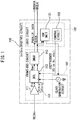
- FIG. 1 is a block diagram depicting an example of a receiver circuit applying a SerDes (Serializer / Deserializer).
- a receiver circuit 100 applying a SerDes receives and processes a serial signal (serial data) RXIN input via a transmission line, and outputs a parallel data RXDATA and a clock RXCLK.
- the receiver circuit 100 includes a front-end circuit 101, a logic circuit 102 and a clock generation circuit 103.
- the front-end circuit 101 includes an amplifier circuit 111, a decision feedback equalizer (DFE) and a demultiplexer (DMUX) 113.
- the amplifier circuit 111 amplifies the serial signal RXIN input thereto, and outputs to the DFE (equalizer) 112.
- the DFE 112 receives the amplified serial signal (Vin, Vin-p, Vin-n), determines "0" and "1” of data, and outputs the determined data (Dout) accompanied with a clock to the DMUX 113 subsequent to the DFE 112.
- the DMUX 113 receives the data and clock from the DFE 112, performs a serial / parallel conversion, and outputs a divided receive clock RXCLK and received parallel data RXDATA synchronized with the receive clock RXCLK. Further, an output signal of the front-end circuit 101 is input to a clock data recovery (CDR) unit 121 of the logic circuit 102.
- CDR clock data recovery
- the CDR unit (CDR logic circuit) 121 performs a timing control of the clock based on the output signal of the front-end circuit 101 (received data), generates a data capture clock via the clock generation circuit 103, and outputs the data capture clock to the DFE 112.
- the DFE 112 performs a sampling of the input serial data by a preferable timing, and performs the above described determination of "0" and "1" of the data.
- control signals (equalizing coefficients K1 to Kn, etc.) for driving the DFE as an equalizer circuit may be generated by a control circuit 122 in the logic circuit 102, but it is also possible to provide the control signals from an external.
- FIG. 2 is a block diagram depicting an example of an integrated circuit device applying the receiver circuit depicted in FIG. 1 .
- an integrated circuit device (semiconductor chip) 1 includes a receiver circuit 100, a transmitter circuit 200 and an internal circuit (user circuit) 300.
- the receiving circuit 100 is the same as that described with reference to FIG. 1 , and receives the serial signal RXIN and performs a serial / parallel conversion, and outputs the received parallel data RXDATA and the receive clock RXCLK to the internal circuit 300.
- the transmitter circuit 200 receives transmit parallel data TXDARA and a transmit clock TXCLK output from the internal circuit 300, performs a parallel/serial conversion, and outputs a serial signal TXOUT.
- the receiver circuit 100 converts input high speed (e.g., several tens of GHz or higher) serial data RXIN into low speed (e.g., lower than 1 GHz) parallel data RXDATA which may be processed by the internal circuit 300, and outputs the converted parallel data RXDATA to a transmission line.
- the transmitter circuit 200 converts low speed (e.g., lower than 1 GHz) parallel data TXDATA output from the internal circuit 300 into high speed (e.g., several tens of GHz or higher) serial data TXOUT, and outputs the converted serial data TXOUT to the transmission line.
- the integrated circuit device transmits and receives high-speed serial data via board wirings to and from other integrated circuit devices mounted on the same substrate.
- a first system (block) including an integrated circuit device is, for example, separated by a predetermined distance (e.g., several cm to several km) from a second system including another integrated circuit device, and high speed serial data transmission and reception may be performed between the first and second devices via a communication cable.
- the application of the integrated circuit device is not limited above, but the integrated circuit device may be widely applied.
- the integrated circuit device 1 includes the internal circuit 300 accompanied with the receive circuit 100 and the transmitter circuit 200, however, the integrated circuit device 1 may be provided as an I/O (Input / Output) chip including both the receive circuit 100 and the transmitter circuit 200.
- I/O Input / Output
- a pulse including a length of a period of a symbol (code) of the serial signal is, for example, temporally dispersed, by a band limitation of a transmission line (boar wiring, communication cable, etc.) where signals are transmitted from a transmitter circuit 200 of an optional integrated circuit device 1 to a receiver circuit 100 of another integrated circuit device 1.
- a pulse including a symbol period is temporally dispersed, and an interference may be caused in subsequent symbols.
- This phenomenon is known as an inter-symbol interference (ISI).
- ISI inter-symbol interference
- a circuit including a function of increasing a transmission (reception) signal accuracy by removing (reducing) the ISI is referred as an equalizer circuit, and the DFE 112 described above is an example of the equalizer circuit.
- the ISI applied to symbols at a specific timing is determined based on a previous (past) symbol sequence.
- the DFE decision feedback equalizer
- the DFE is used to add determination results of past symbol sequences by weighting respective magnitudes of influences of previous symbols, obtains an estimated value for removing the ISI, subtracts the estimated value from the input signal, and performs a determination by using the comparator circuit.
- FIG. 3 is a block diagram depicting an example of a DFE in the receiver circuit depicted in FIG. 1 , and the DFE handles a serial signal of binary single-ended signal (e.g., NRZ (Non-Return-to-Zero) signal).
- the DFE 20 (112) depicted in FIG. 3 may be called as an n taps (n-tap) DFE for removing (compensating) the influences of the ISI due to previous n symbols from a current symbol.
- n is an integer of 1 or more
- equalizing coefficients K1 to Kn may be set to various values based on, for example, characteristics of a signal line where an input serial signal Vin is transmitted.
- the equalizing coefficients K1 to Kn may be set to fixed values based on characteristics of a signal line where the serial signal RXIN is transmitted or set to fixed values based on periodically measuring characteristics of the signal line.
- the equalizing coefficients K1 to Kn may be dynamically set to values based on characteristics until receiving an immediate preceding symbol by measuring in real time.
- the DFE 20 includes a comparator circuit 22, a flip-flop 23 for holding an output signal (current symbol), n flip-flops 24-1 to 24-n which hold past n symbols, and multiplexer circuits 25-1 to 25-n. Furthermore, the DFE 20 includes n adder circuits (summers) 21-1 to 21-n.
- a configuration including the respective flip-flops 24-1 to 24-n and the multiplexer circuits 25-1 to 25-n is constituted as an inter-symbol interference removal unit (latch circuit + DAC (digital / analog converter)) 26. Therefore, in the n-tap DFE 20, n inter-symbol interference removal units 26 may be included.
- flip-flops (latch circuits) 24-1 to 24-n in respective inter-symbol interference removal unit 26 are connected in series and functioned as a shift register for holding data until past n-th previous symbols.
- the flip-flop (latch circuit) 23 holds an output signal of the comparator circuit 22, and outputs to an external (e.g., DMUX 113 depicted in FIG. 1 ) as data Dout.
- the adder circuit 21-1 adds together inter-symbol interferences (subtracts an estimated value EV) due to past n data caused by n inter-symbol interference removal units 26 to an input signal Vin, and removes influence of inter-symbol interferences of the past n data. Note that, in FIG. 3 , an output signal of each of the inter-symbol interference removal units 26 is sequentially added by a preceding adder circuit 21-2, 21-3, ..., however, the features thereof are not limited to such a configuration.
- the estimated value EV of the ISI (sum of past n data caused by n inter-symbol interference removal units 26) is subtracted from the serial signal Vin input from the external by the adder circuit 21-1. Further, an output signal of the adder circuit 21-1, where interference of the ISI may be removed (reduced), is sampled and quantized by the comparator circuit 22, and is output as output data (digital data) Dout via the flip-flop 23. Note that, as described with reference to FIG. 1 , the output data Dout of the DFE 20 (112) is input to a subsequent DMUX (113), and wherein serial / parallel conversion or the like may be performed.
- an output signal of the comparator circuit 22 is input to a first flip-flop 24-1 of the n flip-flops 24-1 to 24-n which are connected in series.
- the flip-flops 24-1 to 24-n fetch data, for example, in synchronization with a determined symbol clock (data sampling clock), and constitute an n-bit shift register. Therefore, the flip-flops 24-1 to 24-n hold data of the last n symbols.
- the number of data used for the ISI estimation is n
- the ISI caused by n unit intervals (UI: 1 symbol time which is defined by a reciprocal of a baud rate) may be removed.
- FIG. 4 is a block diagram depicting another example of the DFE in the receiver circuit depicted in FIG. 1 , and corresponds to a DFE30 handling a differential (complementary) signal instead of the single-ended signal handled by the DFE20 depicted in FIG. 3 .
- the DFE 30 (112) depicted in FIG. 4 is a n-tap DFE and includes a substantially same structure of the DFE20 depicted in FIG. 3 .
- a determination result of the comparator circuit 22 (32) is a binary "0" or "1", typically corresponding to a voltage of a minus (-) or an plus (+) state of a voltage of the serial signal Vin.
- the sign is considered as a sign of an input signal against the signal ground
- the DFE 30 handling the differential signal depicted in FIG. 4 the sign is considered as a sign of the differential signal.
- outputs of respective inter-symbol interference removal units 26 (36) are gathered and added to the input signal Vin (Vin-p, Vin-n) by the adder circuit 21-1 (31-1).
- output signals of the multiplexer circuits 25-1 to 25-n (35-1 to 35-n) are current signals
- output lines from respective output terminals of the multiplexer circuits 25-1 to 25-n (35-1 to 35-n) may be physically connected to input lines of corresponding terminals of the adder circuit 21-1 (31-1), for example, without providing dedicated adder circuits when the output signals are voltage signals.
- signals input to the adder circuits 21-1 to 21-n are typically analog signals used as current or voltage signals, and DACs (multiplexer circuits 25-1 to 25-n (35-1 to 35-n)) may be used to output analog signals based on the coefficients K1, K2, ..., Kn. Note that, in the DFE30 depicted in FIG. 4 , output signals of the adder circuits 31-1, 31-2, ...
- DACs 35-1, 35-2, ... may be differential signals, and an amplitude (signal amplitude) of the differential signal may be represented by a difference between a pair of signals.
- switching the sign of the differential signal may be realized by changing the differential signal from each other, and therefore a differential signal may be generally applied to an electronic circuit.
- FIG. 5 is a block diagram depicting an example of an inter-symbol interference removal unit in the DFE depicted in FIG. 4 .
- the inter-symbol interference removal unit 5 (36) includes a latch circuit (flip-flop) 51, a DAC (digital / analog converter) 52, a switch circuit 53, and an exclusive OR circuit (XOR gate) 54.
- the DAC as a current DAC
- the analog signal as a differential current signal (e.g., an output signal of the switch circuit is a differential current output signal Iout, Ioutx). Nevertheless, it may be possible to apply a voltage signal and a single-ended signal.
- the flip-flop 51 is a delay circuit used to delay (and hold) a preceding data Dn-1 and output as an output data Dn
- the XOR gate 54 performs an exclusive OR of the output data Dn and code information sign(Kn) of the equalizing coefficient Kn. Note that, in the code information sign(Kn) of the equalizing coefficient Kn, for example, data "0" indicates that the sign is positive, and data "1" indicates that the sign is negative.
- the current DAC 52 receives absolute value information mag(Kn) of the equalizing coefficient Kn, and output a corresponding signal to the switch circuit 53.
- the switch circuit 53 selects an output of the current DAC 52 based on the output of the XOR gate 54, and output as a current output signal Iout or Ioutx.
- the inter-symbol interference removal unit 5 (36) depicted in FIG. 5 processes the output data Dn and the code information sign(Kn) of the equalizing coefficient Kn by using the XOR gate 54, and obtains a multiplication result as their codes. Further, an output of the current DAC 52, which outputs the absolute value information mag(Kn) of the equalizing coefficient Kn as a current signal, is connected to the switch circuit 53 for selecting one of two output terminals, and an output signal of the XOR gate 54 is used as a control signal of the switch circuit 53.
- the two output terminals (current signal Iout, Ioutx) of the switch circuit 53 are connected to, for example, addition terminals (+) and subtraction terminals (-) of the adder circuits 31-2, 31-3, ... depicted in FIG. 4 as described above.
- the switch circuit 53 selects whether a current signal output from the current DAC 52 to one of terminals (+, -) of the adder circuits 31-2, 31-3, ..., so that a sign of the current output applied to the adder circuits 31-2, 31-3, ... is changed.
- the current signal Iout is, for example, grouped with the current signal Iout of the other inter-symbol interference removal unit 36 (5), and input to the addition terminal (+) of the adder circuit 31-1.
- the current signal Ioutx is, for example, grouped with the current signal Ioutx of the other inter-symbol interference removal unit 36, and input to the subtraction terminal (-) of the adder circuit 31-1.
- the delay circuit (latch circuit) 51 is a flip-flop (D-type flip-flop) as an example, and it may be possible to replace it by a various circuit having an equivalent function.
- the DFE (decision feedback equalizer) 30 is used to remove (reduce) influences of the ISI caused by previous symbols from input signals Vin-p, Vin-n, and perform quantization by the comparator 32, when outputs (Iout, Ioutx) of respective inter-symbol interference removal units 36 reach to the adder circuit 31-1. Therefore, a delay time due to a signal based on an output of the latch circuit 51 for holding data previously determined by the comparator circuit 32 reaches to the adder circuit 31-1 (31-2, 31-3, 7) is required within a time (1 UI) for determining the output of the adder circuit 31-1 by the comparator 32. Specifically, an upper limit of data rate which may be processed by the delay time is defined.
- the switch circuit 53 is controlled by an output signal of XOR gate 54 which performs an exclusive OR of the output data Dn and the code information sign(Kn) of the coefficient Kn.
- an operation delay of the XOR gate 54 defined from outputting the data Dn until outputting current signals Iout, Ioutx is included, so that an operation speed of the circuit may be limited. As the result, it has become difficult for a high-speed signal transmission of data rate, for example, several tens GBps.
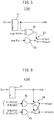
- FIG. 6 is a block diagram depicting a first embodiment of an inter-symbol interference removal unit in a DFE according to the present embodiments.
- an inter-symbol interference removal unit 6 depicted in FIG. 6 is, for example, applied to the inter-symbol interference removal unit 36 depicted in FIG. 4 described above.
- This matter for the first embodiment may be also the same as inter-symbol interference removal units 7 and 8 of a second embodiment and a third embodiment, which will be described later.
- each adder circuit 31-2, 31-3, ...) may be realized by applying well-known circuit configurations.
- an equalizer circuit, a receiver circuit and an integrated circuit device of the present embodiment may be realized by applying an inter-symbol interference removal unit according to the first to third embodiments described later.
- the inter-symbol interference removal unit 6 (36) includes a flip-flop (latch circuit) 61, current DACs (digital / analog converter circuits) 62, 63, and a switch circuit 64.
- the flip-flop 61 is used as a delay circuit which delays (and holds) a preceding data Dn-1 and outputs as an output data Dn, and the switch circuit 64 selects output signals of the current DACs 62, 63 based on the output data Dn, and outputs as a current output signal Iout or Ioutx.
- the current DAC (first DAC) 62 When an equalizing coefficient Kn is larger than zero (Kn > 0), i.e., when Kn is a positive value, the current DAC (first DAC) 62 receives information indicating Kn (absolute value of Kn), and when Kn is equal to or lower than zero (Kn ⁇ 0), i.e., when Kn is a negative value or zero, the current DAC 62 receives the information indicating Kn is zero ("0"), and outputs a corresponding current signal (first signal), respectively.
- the current DAC (second DAC) 63 receives the information indicating Kn is zero
- the current DAC 63 receives information indicating -Kn (absolute value of Kn), and outputs a corresponding current signal (second signal), respectively. Therefore, in two current DACs 62, 63, absolute value information of Kn is supplied to one of the DACs, and information indicating the equalizing coefficient is zero ("0") is supplied to the other of the DACs, in accordance with the sign of the equalizing coefficient Kn.
- the switch circuit 64 receives outputs of the current DACs 62 and 63 (first signal and second signal), and selects signals to be output as current output signals Iout and Ioutx based on an output signal (Dn) of the flip-flop 61.
- two output terminals (current signals Iout, Ioutx) of the switch circuit 64 are, for example, connected to an addition terminal (+) and a subtraction terminal (-) of the adder circuits 31-2, 31-3, ... depicted in FIG. 4 described above.
- the switch circuit 64 is adapted to switch whether current signals output from the current DACs 62 and 63 to terminals (+, -) of the adder circuits 31-2, 31-3, ...
- the current signals Iout are, for example, grouped with a current signal Iout of the other inter-symbol interference removal units 36 (6), and supplied to an addition terminal (+) of the adder circuit 31-1.
- the current signals Ioutx are, for example, grouped with a current signal Ioutx of the other inter-symbol interference removal units 36, and supplied to a subtraction terminal (-) of the adder circuit 31-1.
- the delay circuit (latch circuit) 61 is explained by applying a flip-flop, however, the delay circuit may be replaced by various circuits including an equivalent function.
- the current DAC 62, 63 output, for example, a predetermined current value (current signal) for code information sign(Kn) of a predetermined coefficient Kn, and the switch circuit 64 is directly controlled by an output data (Dn) of the flip-flop 61. Therefore, for example, it is possible to omit the delay due to the XOR gate 54 in the inter-symbol interference removal unit 5 depicted in FIG. 5 described above, and it becomes possible to increase an operation speed (high-speed data rate) of the circuit.
- the output data Dn is used to select two signals, and a circuit scale of the switch circuit depicted in FIG. 6 becomes, for example, twice of a circuit scale of the switch circuit 53 depicted in FIG. 5 . Therefore, a consumption power is increased, however, no practical problem may be caused.
- FIG. 7 is a block diagram depicting a second embodiment of the inter-symbol interference removal unit in the DFE according to the present embodiments.
- an inter-symbol interference removal unit 7 (36) includes a flip-flop 71, a current DAC72 and switch circuits 73, 74.
- the flip-flop 71 is the similar to the flip-flop 61 of the first embodiment described above, and an output data Dn controls the switch circuit (first switch circuit) 73.
- the second switch circuit 74 is controlled based on code information sign(Kn) of an equalizing coefficient Kn.
- the current DAC72 receives absolute value information mag(Kn) of the equalizing coefficient Kn, and outputs a corresponding current signal (third signal).
- the first switch circuit 73 is controlled based on the output data Dn from the flip-flop 71, and an output of the first switch circuit 73 is input to the second switch circuit 74.
- the second switch circuit 74 selects an output of the first switch circuit 73 based on the code information sign(Kn) of the equalizing coefficient Kn, and outputs a signal as a current output signal Iout or Ioutx.
- the current DAC 72 also outputs, for example, a predetermined current signal for absolute value information mag(Kn) of a predetermined coefficient Kn.
- the first switch circuit 73 is directly controlled by the output data Dn from the flip-flop 71, and the second switch circuit 74 is controlled by the code information sign(Kn) of the predetermined coefficient Kn, Therefore, as in the first embodiment described above, for example, it may be possible to omit the XOR gate 54 in the inter-symbol interference removal unit 5 depicted in FIG. 5 described above, and also possible to increase an operation speed of the circuit.
- inter-symbol interference removal units 7 of second embodiment two stages of switch circuits for selecting an output signal of the current DAC72 may be provided in series. Therefore, an output level of the current DAC72 may be reduced and an operation speed thereof may be decreased, however, no practical problem may be caused.
- FIG. 8 is a block diagram depicting a third embodiment of the inter-symbol interference removal unit in the DFE according to the present embodiments.
- an inter-symbol interference removal unit 8 (36) includes a flip-flop 81, a current DAC 82, a switch circuit 83 and an XOR gates 84, 85.
- the XOR gate (second exclusive OR circuit) 85 receives code information sign(Kn) of an equalizing coefficient for a current symbol (data Dn) and code information sign(Kn-1) of an equalizing coefficient for an immediate preceding symbol (Dn-1), and takes an exclusive OR thereof.
- the XOR gate (first exclusive OR circuit) 84 takes an exclusive OR of an output signal (second value) of the XOR gate 85 and a multiplication value (first value) of multiplying data Dn-1 of the immediate preceding symbol and the code information sign(Kn-1) of the equalizing coefficient Kn-1 thereof.
- the XOR gate 84 take an exclusive OR of the first value (sign(Kn-1) ⁇ Dn-1) and the second value output from the XOR gate 85, and outputs to the flip-flop 81, wherein the first value is obtained by multiplying data immediate preceding symbol of an output of the comparator circuit 32 and code information of an equalizing coefficient thereof.
- the XOR gate 85 takes, for example, an exclusive OR of code information sign(Kn) of a predetermined coefficient Kn and code information sign(Kn-1) of a coefficient Kn-1, and therefore no delay may be caused.
- the XOR gate 85 may be possible not to internally provide into the inter-symbol interference removal unit 8, and previously performs an exclusive OR process in external, and a processed value (second value) may be input to the XOR gate 84.
- the first value (sign(Kn-1) ⁇ Dn-1) input to the XOR gate 84 is obtained based on the immediate preceding symbol, and therefore a delay may not caused by the XOR gate 84, similar to the XOR gate 85.
- the flip-flop 81 receives an input signal (output signal of XOR gate 84) and delays (and holds), and outputs a signal sign(Kn) ⁇ Dn.
- an output signal of the XOR gate 84 which is processed as described above, is input to the flip-flop (delay circuit) 81 without using data Dn-1 of the immediate preceding symbol different from the first and second embodiments as described above.
- the switch circuit 83 selects an output signal (fourth signal) of the current DAC 82 based on an output signal (sign(Kn) ⁇ Dn) of the flip-flop 81, and outputs as a current output signal Iout or Ioutx.
- the switch circuit 83 is directly controlled by the output signal of the flip-flop 81, and therefore it is possible to eliminate a delay due to the XOR gate 54 of the inter-symbol interference removal unit 5 depicted in FIG. 5 .
- the switch circuit 83 only selects one of two output terminals (Iout, Ioutx), and therefore it may not cause problems such as an increase of a consumption power in the first embodiment.
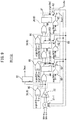
- FIG. 9 is a block diagram depicting an example of a DFE applying the third embodiment of the inter-symbol interference removal unit depicted in FIG. 8 , and wherein the inter-symbol interference removal unit 8 depicted in FIG. 8 is applied to the inter-symbol interference removal unit 36 of the DFE 30 (112) depicted in FIG. 4 .
- a current DAC 82, signals input to XOR gates 84, 85, and a control signal of a switch circuit 83 are shifted depending on corresponding symbols. Further, in FIG.
- the DAC 82 is constituted as a current DAC, differential current output signals Iout, Ioutx from each of the inter-symbol interference removal units 36 (8) are grouped and input to an addition terminal (+) and a subtraction terminal (-) of an adder circuit 31-1, by physically connecting output lines of respective output terminals of a switch circuit 83 of each of the inter-symbol interference removal units 36 (8) to input lines corresponding to the addition terminal (+) and subtraction terminal (-) of the adder circuit 31-1.
- the circuit configuration of the physical connected described above functions as an adder circuit.
- each of the first to third embodiments may be of course to apply, for example, to the DFE 20 processing a single-ended signal as depicted in FIG. 3 , or the DFE compensating the SIS by using voltage signals.
Landscapes
- Engineering & Computer Science (AREA)
- Computer Networks & Wireless Communication (AREA)
- Signal Processing (AREA)
- Power Engineering (AREA)
- Physics & Mathematics (AREA)
- Mathematical Physics (AREA)
- Cable Transmission Systems, Equalization Of Radio And Reduction Of Echo (AREA)
- Dc Digital Transmission (AREA)
Abstract
Description
- Embodiments discussed herein relate to an equalizer circuit, a receiver circuit, and an integrated circuit device.
- Recently, in signal transmission among integrated circuit devices (LSI: Large-Scale Integrated circuits) mounted on a board (printed board) or signal transmission between boards over a network or signal transmission among blocks or systems, for example, a gigabit SerDes (Serializer / Deselializer) has been used. This SerDes is, for example, used to convert low speed parallel data into high speed serial data in a signal transmission side, the high speed serial data being transferred to a signal reception side via a signal line, and used to convert the high speed serial data into low speed parallel data in the signal reception side, etc., the converted low speed parallel data being processed in the signal reception side.
- For example, in the case of receiving a serial signal via a transmission line such as a board wiring or a communication cable, etc., a pulse having a length of a period of a code (symbol) is temporally dispersed. Specifically, for example, in a high-speed signal transmission exceeding a few GBps (Giga Bit per second), the pulse having a symbol period is temporally dispersed by the band limitation of the transmission line, and an interference may be caused in subsequent symbols. This phenomenon has been known as an inter-symbol interference (ISI), and a decision feedback equalizer (DFE) may be used to increase an accuracy of the signal transmission (signal reception) by decreasing the ISI.
- Incidentally, in the prior art, various techniques have been proposed to enable a high speed signal transmission by reducing an influence of the inter-symbol interference (inter-code interference).
-
- [Patent Document 1] Japanese Laid-open Patent Publication No.
2015-192200 - [Patent Document 2] International Publication No.
WO 2015/125282 - [Patent Document 3] Japanese Laid-open Patent Publication No.
2001-044895 - Conventionally, the various techniques have been proposed to enable the high speed signal transmission by reducing the influence of the inter-symbol interference. However, for example, various factors of causing a delay may be remained in an inter-symbol interference removal unit of the DFE, and therefore it is difficult to realize a further speed up required for the high speed signal transmission in recent years.
- An object of embodiments discussed in this application is to provide o an equalizer circuit, a receiver circuit and an integrated circuit device capable of enabling a high-speed data rate by reducing an influence of inter-symbol interference.
- According to an aspect of the embodiments, there is provided an equalizer circuit including a first adder circuit configured to add an input signal, a comparator circuit configured to compare an output of the first adder circuit, a latch circuit configured to latch data output from the comparator circuit, first and second digital / analog converter circuits, and a switch circuit.
- The first digital / analog converter circuit is configured to output a first signal corresponding to an absolute value of an equalizing coefficient, when the equalizing coefficient is a positive value, and the second digital / analog converter circuit is configured to output a second signal corresponding to an absolute value of the equalizing coefficient, when the equalizing coefficient is a negative value.
- The switch circuit is configured to switch a connection between an output of the first digital / analog converter circuit and an output of the second digital / analog converter circuit, and a connection between an addition terminal and a subtraction terminal of the first adder circuit, based on the data latched in the latch circuit.
- According to embodiments of an equalizer circuit, a receiver circuit and an integrated circuit device disclosed herein, it is possible to enable a high-speed data rate by reducing an influence of inter-symbol interference.
-
-
FIG. 1 is a block diagram depicting an example of a receiver circuit applying a SerDes. -
FIG. 2 is a block diagram depicting an example of an integrated circuit device applying the receiver circuit depicted inFIG. 1 . -
FIG. 3 is a block diagram depicting an example of a DFE in the receiver circuit depicted inFIG. 1 . -
FIG. 4 is a block diagram depicting another example of the DFE in the receiver circuit depicted inFIG. 1 . -
FIG. 5 is a block diagram depicting an example of an inter-symbol interference removal unit in the DFE depicted inFIG. 4 . -
FIG. 6 is a block diagram depicting a first embodiment of an inter-symbol interference removal unit in a DFE according to the present embodiments. -
FIG. 7 is a block diagram depicting a second embodiment of the inter-symbol interference removal unit in the DFE according to the present embodiments. -
FIG. 8 is a block diagram depicting a third embodiment of the inter-symbol interference removal unit in the DFE according to the present embodiments. -
FIG. 9 is a block diagram depicting an example of a DFE applying the third embodiment of the inter-symbol interference removal unit depicted inFIG. 8 . - First, before describing embodiments of an equalizer circuit, a receiver circuit and an integrated circuit device, an example of an equalizer circuit, a receiver circuit and an integrated circuit device, an example of the equalizer circuit, receiver circuit and integrated circuit and problems thereof will be described with reference to
FIG. 1 to FIG. 5 .FIG. 1 is a block diagram depicting an example of a receiver circuit applying a SerDes (Serializer / Deserializer). - As depicted in
FIG. 1 , for example, areceiver circuit 100 applying a SerDes receives and processes a serial signal (serial data) RXIN input via a transmission line, and outputs a parallel data RXDATA and a clock RXCLK. Thereceiver circuit 100 includes a front-end circuit 101, alogic circuit 102 and aclock generation circuit 103. - The front-
end circuit 101 includes anamplifier circuit 111, a decision feedback equalizer (DFE) and a demultiplexer (DMUX) 113. Theamplifier circuit 111 amplifies the serial signal RXIN input thereto, and outputs to the DFE (equalizer) 112. The DFE 112 receives the amplified serial signal (Vin, Vin-p, Vin-n), determines "0" and "1" of data, and outputs the determined data (Dout) accompanied with a clock to theDMUX 113 subsequent to the DFE 112. - The
DMUX 113 receives the data and clock from the DFE 112, performs a serial / parallel conversion, and outputs a divided receive clock RXCLK and received parallel data RXDATA synchronized with the receive clock RXCLK. Further, an output signal of the front-end circuit 101 is input to a clock data recovery (CDR)unit 121 of thelogic circuit 102. - The CDR unit (CDR logic circuit) 121 performs a timing control of the clock based on the output signal of the front-end circuit 101 (received data), generates a data capture clock via the
clock generation circuit 103, and outputs the data capture clock to the DFE 112. The DFE 112 performs a sampling of the input serial data by a preferable timing, and performs the above described determination of "0" and "1" of the data. Note that, control signals (equalizing coefficients K1 to Kn, etc.) for driving the DFE as an equalizer circuit may be generated by acontrol circuit 122 in thelogic circuit 102, but it is also possible to provide the control signals from an external. -
FIG. 2 is a block diagram depicting an example of an integrated circuit device applying the receiver circuit depicted inFIG. 1 . As depicted inFIG. 2 , an integrated circuit device (semiconductor chip) 1 includes areceiver circuit 100, atransmitter circuit 200 and an internal circuit (user circuit) 300. Thereceiving circuit 100 is the same as that described with reference toFIG. 1 , and receives the serial signal RXIN and performs a serial / parallel conversion, and outputs the received parallel data RXDATA and the receive clock RXCLK to theinternal circuit 300. Thetransmitter circuit 200 receives transmit parallel data TXDARA and a transmit clock TXCLK output from theinternal circuit 300, performs a parallel/serial conversion, and outputs a serial signal TXOUT. - Specifically, the
receiver circuit 100 converts input high speed (e.g., several tens of GHz or higher) serial data RXIN into low speed (e.g., lower than 1 GHz) parallel data RXDATA which may be processed by theinternal circuit 300, and outputs the converted parallel data RXDATA to a transmission line. Further, thetransmitter circuit 200 converts low speed (e.g., lower than 1 GHz) parallel data TXDATA output from theinternal circuit 300 into high speed (e.g., several tens of GHz or higher) serial data TXOUT, and outputs the converted serial data TXOUT to the transmission line. - Note that the integrated circuit device, for example, transmits and receives high-speed serial data via board wirings to and from other integrated circuit devices mounted on the same substrate. Further a first system (block) including an integrated circuit device is, for example, separated by a predetermined distance (e.g., several cm to several km) from a second system including another integrated circuit device, and high speed serial data transmission and reception may be performed between the first and second devices via a communication cable. Incidentally, the application of the integrated circuit device is not limited above, but the integrated circuit device may be widely applied.
- Further, in
FIG. 2 , theintegrated circuit device 1 includes theinternal circuit 300 accompanied with thereceive circuit 100 and thetransmitter circuit 200, however, theintegrated circuit device 1 may be provided as an I/O (Input / Output) chip including both thereceive circuit 100 and thetransmitter circuit 200. In addition, it may be possible to provide various forms such as only thereceiver circuit 100, only thetransmitter circuit 200, and an IP (Intellectual Property) macro constituted by a plurality ofreceiver circuits 100 andtransmitter circuits 200. - Incidentally, a pulse including a length of a period of a symbol (code) of the serial signal is, for example, temporally dispersed, by a band limitation of a transmission line (boar wiring, communication cable, etc.) where signals are transmitted from a
transmitter circuit 200 of an optionalintegrated circuit device 1 to areceiver circuit 100 of anotherintegrated circuit device 1. Specifically, in a high-speed signal transmission, a pulse including a symbol period is temporally dispersed, and an interference may be caused in subsequent symbols. This phenomenon is known as an inter-symbol interference (ISI). Here, a circuit including a function of increasing a transmission (reception) signal accuracy by removing (reducing) the ISI is referred as an equalizer circuit, and theDFE 112 described above is an example of the equalizer circuit. - Specifically, the ISI applied to symbols at a specific timing (current timing) is determined based on a previous (past) symbol sequence. Here, the DFE (decision feedback equalizer) is used to add determination results of past symbol sequences by weighting respective magnitudes of influences of previous symbols, obtains an estimated value for removing the ISI, subtracts the estimated value from the input signal, and performs a determination by using the comparator circuit.
-
FIG. 3 is a block diagram depicting an example of a DFE in the receiver circuit depicted inFIG. 1 , and the DFE handles a serial signal of binary single-ended signal (e.g., NRZ (Non-Return-to-Zero) signal). The DFE 20 (112) depicted inFIG. 3 may be called as an n taps (n-tap) DFE for removing (compensating) the influences of the ISI due to previous n symbols from a current symbol. Here, n is an integer of 1 or more, equalizing coefficients K1 to Kn may be set to various values based on, for example, characteristics of a signal line where an input serial signal Vin is transmitted. Note that, for example, the equalizing coefficients K1 to Kn may be set to fixed values based on characteristics of a signal line where the serial signal RXIN is transmitted or set to fixed values based on periodically measuring characteristics of the signal line. Alternatively, for example, the equalizing coefficients K1 to Kn may be dynamically set to values based on characteristics until receiving an immediate preceding symbol by measuring in real time. - As depicted in
FIG. 3 , theDFE 20 includes acomparator circuit 22, a flip-flop 23 for holding an output signal (current symbol), n flip-flops 24-1 to 24-n which hold past n symbols, and multiplexer circuits 25-1 to 25-n. Furthermore, theDFE 20 includes n adder circuits (summers) 21-1 to 21-n. Here, in each stage, a configuration including the respective flip-flops 24-1 to 24-n and the multiplexer circuits 25-1 to 25-n is constituted as an inter-symbol interference removal unit (latch circuit + DAC (digital / analog converter)) 26. Therefore, in the n-tap DFE 20, n inter-symbolinterference removal units 26 may be included. Note that, flip-flops (latch circuits) 24-1 to 24-n in respective inter-symbolinterference removal unit 26 are connected in series and functioned as a shift register for holding data until past n-th previous symbols. The flip-flop (latch circuit) 23 holds an output signal of thecomparator circuit 22, and outputs to an external (e.g.,DMUX 113 depicted inFIG. 1 ) as data Dout. - The adder circuit 21-1 adds together inter-symbol interferences (subtracts an estimated value EV) due to past n data caused by n inter-symbol
interference removal units 26 to an input signal Vin, and removes influence of inter-symbol interferences of the past n data. Note that, inFIG. 3 , an output signal of each of the inter-symbolinterference removal units 26 is sequentially added by a preceding adder circuit 21-2, 21-3, ..., however, the features thereof are not limited to such a configuration. - Specifically, as depicted in
FIG. 3 , in theDFE 20, the estimated value EV of the ISI (sum of past n data caused by n inter-symbol interference removal units 26) is subtracted from the serial signal Vin input from the external by the adder circuit 21-1. Further, an output signal of the adder circuit 21-1, where interference of the ISI may be removed (reduced), is sampled and quantized by thecomparator circuit 22, and is output as output data (digital data) Dout via the flip-flop 23. Note that, as described with reference toFIG. 1 , the output data Dout of the DFE 20 (112) is input to a subsequent DMUX (113), and wherein serial / parallel conversion or the like may be performed. - Further, as depicted in
FIG. 3 , an output signal of thecomparator circuit 22 is input to a first flip-flop 24-1 of the n flip-flops 24-1 to 24-n which are connected in series. Here, the flip-flops 24-1 to 24-n fetch data, for example, in synchronization with a determined symbol clock (data sampling clock), and constitute an n-bit shift register. Therefore, the flip-flops 24-1 to 24-n hold data of the last n symbols. Specifically, in the n taps DFE20 depicted inFIG. 3 , the number of data used for the ISI estimation (number past symbols) is n, and the ISI caused by n unit intervals (UI: 1 symbol time which is defined by a reciprocal of a baud rate) may be removed. -
FIG. 4 is a block diagram depicting another example of the DFE in the receiver circuit depicted inFIG. 1 , and corresponds to a DFE30 handling a differential (complementary) signal instead of the single-ended signal handled by the DFE20 depicted inFIG. 3 . Specifically, as is apparent from a comparison betweenFIG. 4 andFIG. 3 , the DFE 30 (112) depicted inFIG. 4 is a n-tap DFE and includes a substantially same structure of the DFE20 depicted inFIG. 3 . - Next, calculation of an estimated value of the ISI will be explained. First, in the case of an NRZ signal, a determination result of the comparator circuit 22 (32) is a binary "0" or "1", typically corresponding to a voltage of a minus (-) or an plus (+) state of a voltage of the serial signal Vin. For example, in the
DFE 20 handling the single-ended signal depicted inFIG. 3 , the sign is considered as a sign of an input signal against the signal ground, and in theDFE 30 handling the differential signal depicted inFIG. 4 , the sign is considered as a sign of the differential signal. - Further, so as to estimate a magnitude of the ISI influencing to a determination of current symbol by the past symbols, in the n-tap DFE 20 (30), for each of coefficients K1, ..., Kn, which represents the influence of the past data, for example, "-1" is made to correspond to data "0" and "+1" is made to correspond to data "1". In the multiplexer circuits 25-1 to 25-n (35-1 to 35-n), for the coefficients K1, ..., Kn input thereto, the data "0" is multiplied by a sign of "-1" and the data "1" is multiplied by a sign of "+1" (positive), and are wholly integrated by the adder circuits 21-1 to 21-n (31-1 to 31-n). Specifically, outputs of respective inter-symbol interference removal units 26 (36) are gathered and added to the input signal Vin (Vin-p, Vin-n) by the adder circuit 21-1 (31-1). Incidentally, when output signals of the multiplexer circuits 25-1 to 25-n (35-1 to 35-n) are current signals, output lines from respective output terminals of the multiplexer circuits 25-1 to 25-n (35-1 to 35-n) may be physically connected to input lines of corresponding terminals of the adder circuit 21-1 (31-1), for example, without providing dedicated adder circuits when the output signals are voltage signals.
- In this way, by subtracting the ISI due to past symbols weighted by equalizing coefficients K1, ..., Kn from the input serial signal Vin (Vin-p, Vin-n), it may be possible to remove (reduce) an influence of the ISI caused by the past symbols. Here, signals input to the adder circuits 21-1 to 21-n (31-1 to 31-n) are typically analog signals used as current or voltage signals, and DACs (multiplexer circuits 25-1 to 25-n (35-1 to 35-n)) may be used to output analog signals based on the coefficients K1, K2, ..., Kn. Note that, in the DFE30 depicted in
FIG. 4 , output signals of the adder circuits 31-1, 31-2, ... and the DACs 35-1, 35-2, ... may be differential signals, and an amplitude (signal amplitude) of the differential signal may be represented by a difference between a pair of signals. Specifically, switching the sign of the differential signal may be realized by changing the differential signal from each other, and therefore a differential signal may be generally applied to an electronic circuit. -
FIG. 5 is a block diagram depicting an example of an inter-symbol interference removal unit in the DFE depicted inFIG. 4 . As depicted inFIG. 5 , the inter-symbol interference removal unit 5 (36) includes a latch circuit (flip-flop) 51, a DAC (digital / analog converter) 52, aswitch circuit 53, and an exclusive OR circuit (XOR gate) 54. In the following descriptions, assuming the DAC as a current DAC, the analog signal as a differential current signal (e.g., an output signal of the switch circuit is a differential current output signal Iout, Ioutx). Nevertheless, it may be possible to apply a voltage signal and a single-ended signal. - The flip-
flop 51 is a delay circuit used to delay (and hold) a preceding data Dn-1 and output as an output data Dn, TheXOR gate 54 performs an exclusive OR of the output data Dn and code information sign(Kn) of the equalizing coefficient Kn. Note that, in the code information sign(Kn) of the equalizing coefficient Kn, for example, data "0" indicates that the sign is positive, and data "1" indicates that the sign is negative. Thecurrent DAC 52 receives absolute value information mag(Kn) of the equalizing coefficient Kn, and output a corresponding signal to theswitch circuit 53. Theswitch circuit 53 selects an output of thecurrent DAC 52 based on the output of theXOR gate 54, and output as a current output signal Iout or Ioutx. - Therefore, the inter-symbol interference removal unit 5 (36) depicted in
FIG. 5 processes the output data Dn and the code information sign(Kn) of the equalizing coefficient Kn by using theXOR gate 54, and obtains a multiplication result as their codes. Further, an output of thecurrent DAC 52, which outputs the absolute value information mag(Kn) of the equalizing coefficient Kn as a current signal, is connected to theswitch circuit 53 for selecting one of two output terminals, and an output signal of theXOR gate 54 is used as a control signal of theswitch circuit 53. The two output terminals (current signal Iout, Ioutx) of theswitch circuit 53 are connected to, for example, addition terminals (+) and subtraction terminals (-) of the adder circuits 31-2, 31-3, ... depicted inFIG. 4 as described above. Specifically, theswitch circuit 53 selects whether a current signal output from thecurrent DAC 52 to one of terminals (+, -) of the adder circuits 31-2, 31-3, ..., so that a sign of the current output applied to the adder circuits 31-2, 31-3, ... is changed. - Therefore, the current signal Iout is, for example, grouped with the current signal Iout of the other inter-symbol interference removal unit 36 (5), and input to the addition terminal (+) of the adder circuit 31-1. Similarly, the current signal Ioutx is, for example, grouped with the current signal Ioutx of the other inter-symbol
interference removal unit 36, and input to the subtraction terminal (-) of the adder circuit 31-1. Here, the delay circuit (latch circuit) 51 is a flip-flop (D-type flip-flop) as an example, and it may be possible to replace it by a various circuit having an equivalent function. - Incidentally, the DFE (decision feedback equalizer) 30 is used to remove (reduce) influences of the ISI caused by previous symbols from input signals Vin-p, Vin-n, and perform quantization by the
comparator 32, when outputs (Iout, Ioutx) of respective inter-symbolinterference removal units 36 reach to the adder circuit 31-1. Therefore, a delay time due to a signal based on an output of thelatch circuit 51 for holding data previously determined by thecomparator circuit 32 reaches to the adder circuit 31-1 (31-2, 31-3, ...) is required within a time (1 UI) for determining the output of the adder circuit 31-1 by thecomparator 32. Specifically, an upper limit of data rate which may be processed by the delay time is defined. - However, in the inter-symbol interference removal unit 5 (36) depicted in
FIG. 5 , theswitch circuit 53 is controlled by an output signal ofXOR gate 54 which performs an exclusive OR of the output data Dn and the code information sign(Kn) of the coefficient Kn. Specifically, in the inter-symbolinterference removal unit 5, an operation delay of theXOR gate 54 defined from outputting the data Dn until outputting current signals Iout, Ioutx is included, so that an operation speed of the circuit may be limited. As the result, it has become difficult for a high-speed signal transmission of data rate, for example, several tens GBps. - Hereinafter, embodiments of an equalizer circuit, a receiver circuit and an integrated circuit device will be described in detail with reference to the accompanying drawings.
FIG. 6 is a block diagram depicting a first embodiment of an inter-symbol interference removal unit in a DFE according to the present embodiments. Note that an inter-symbolinterference removal unit 6 depicted inFIG. 6 is, for example, applied to the inter-symbolinterference removal unit 36 depicted inFIG. 4 described above. This matter for the first embodiment may be also the same as inter-symbolinterference removal units - Further, as described above, in the following descriptions, assuming a DAC as a current DAC, an analog signal as a differential current signal, however, it is of course that a voltage signal and a single-ended signal may be applied. Note that, when applying a voltage signal, features of each adder circuit (31-2, 31-3, ...) may be realized by applying well-known circuit configurations. Further, an equalizer circuit, a receiver circuit and an integrated circuit device of the present embodiment may be realized by applying an inter-symbol interference removal unit according to the first to third embodiments described later.
- As depicted in
FIG. 6 , the inter-symbol interference removal unit 6 (36) includes a flip-flop (latch circuit) 61, current DACs (digital / analog converter circuits) 62, 63, and aswitch circuit 64. The flip-flop 61 is used as a delay circuit which delays (and holds) a preceding data Dn-1 and outputs as an output data Dn, and theswitch circuit 64 selects output signals of thecurrent DACs - When an equalizing coefficient Kn is larger than zero (Kn > 0), i.e., when Kn is a positive value, the current DAC (first DAC) 62 receives information indicating Kn (absolute value of Kn), and when Kn is equal to or lower than zero (Kn ≤ 0), i.e., when Kn is a negative value or zero, the
current DAC 62 receives the information indicating Kn is zero ("0"), and outputs a corresponding current signal (first signal), respectively. On the other hand, when the equalizing coefficient Kn is equal to or larger than zero (Kn ≥ 0), i.e., when Kn is zero or a positive value, the current DAC (second DAC) 63 receives the information indicating Kn is zero - ("0"), and when Kn is lower than zero (Kn < 0), i.e., when Kn is a negative value, the
current DAC 63 receives information indicating -Kn (absolute value of Kn), and outputs a corresponding current signal (second signal), respectively. Therefore, in twocurrent DACs - The
switch circuit 64 receives outputs of thecurrent DACs 62 and 63 (first signal and second signal), and selects signals to be output as current output signals Iout and Ioutx based on an output signal (Dn) of the flip-flop 61. Here, two output terminals (current signals Iout, Ioutx) of theswitch circuit 64 are, for example, connected to an addition terminal (+) and a subtraction terminal (-) of the adder circuits 31-2, 31-3, ... depicted inFIG. 4 described above. Specifically, theswitch circuit 64 is adapted to switch whether current signals output from thecurrent DACs - Therefore, the current signals Iout are, for example, grouped with a current signal Iout of the other inter-symbol interference removal units 36 (6), and supplied to an addition terminal (+) of the adder circuit 31-1. Similarly, the current signals Ioutx are, for example, grouped with a current signal Ioutx of the other inter-symbol
interference removal units 36, and supplied to a subtraction terminal (-) of the adder circuit 31-1. Note that, in the above descriptions, the delay circuit (latch circuit) 61 is explained by applying a flip-flop, however, the delay circuit may be replaced by various circuits including an equivalent function. - Here, the
current DAC switch circuit 64 is directly controlled by an output data (Dn) of the flip-flop 61. Therefore, for example, it is possible to omit the delay due to theXOR gate 54 in the inter-symbolinterference removal unit 5 depicted inFIG. 5 described above, and it becomes possible to increase an operation speed (high-speed data rate) of the circuit. Note that, in the inter-symbolinterference removal unit 6 of the first embodiment, the output data Dn is used to select two signals, and a circuit scale of the switch circuit depicted inFIG. 6 becomes, for example, twice of a circuit scale of theswitch circuit 53 depicted inFIG. 5 . Therefore, a consumption power is increased, however, no practical problem may be caused. -
FIG. 7 is a block diagram depicting a second embodiment of the inter-symbol interference removal unit in the DFE according to the present embodiments. As depicted inFIG. 7 , an inter-symbol interference removal unit 7 (36) includes a flip-flop 71, a current DAC72 and switchcircuits flop 71 is the similar to the flip-flop 61 of the first embodiment described above, and an output data Dn controls the switch circuit (first switch circuit) 73. Note that thesecond switch circuit 74 is controlled based on code information sign(Kn) of an equalizing coefficient Kn. - The current DAC72 receives absolute value information mag(Kn) of the equalizing coefficient Kn, and outputs a corresponding current signal (third signal). The
first switch circuit 73 is controlled based on the output data Dn from the flip-flop 71, and an output of thefirst switch circuit 73 is input to thesecond switch circuit 74. Thesecond switch circuit 74 selects an output of thefirst switch circuit 73 based on the code information sign(Kn) of the equalizing coefficient Kn, and outputs a signal as a current output signal Iout or Ioutx. - In inter-symbol
interference removal unit 7 of the second embodiment, thecurrent DAC 72 also outputs, for example, a predetermined current signal for absolute value information mag(Kn) of a predetermined coefficient Kn. Further, thefirst switch circuit 73 is directly controlled by the output data Dn from the flip-flop 71, and thesecond switch circuit 74 is controlled by the code information sign(Kn) of the predetermined coefficient Kn, Therefore, as in the first embodiment described above, for example, it may be possible to omit theXOR gate 54 in the inter-symbolinterference removal unit 5 depicted inFIG. 5 described above, and also possible to increase an operation speed of the circuit. Note that, in this inter-symbolinterference removal units 7 of second embodiment, two stages of switch circuits for selecting an output signal of the current DAC72 may be provided in series. Therefore, an output level of the current DAC72 may be reduced and an operation speed thereof may be decreased, however, no practical problem may be caused. -
FIG. 8 is a block diagram depicting a third embodiment of the inter-symbol interference removal unit in the DFE according to the present embodiments. As depicted inFIG. 8 , an inter-symbol interference removal unit 8 (36) includes a flip-flop 81, acurrent DAC 82, aswitch circuit 83 and anXOR gates XOR gate 85 and a multiplication value (first value) of multiplying data Dn-1 of the immediate preceding symbol and the code information sign(Kn-1) of the equalizing coefficient Kn-1 thereof. - Specifically, the
XOR gate 84 take an exclusive OR of the first value (sign(Kn-1) × Dn-1) and the second value output from theXOR gate 85, and outputs to the flip-flop 81, wherein the first value is obtained by multiplying data immediate preceding symbol of an output of thecomparator circuit 32 and code information of an equalizing coefficient thereof. Here, theXOR gate 85 takes, for example, an exclusive OR of code information sign(Kn) of a predetermined coefficient Kn and code information sign(Kn-1) of a coefficient Kn-1, and therefore no delay may be caused. Further, theXOR gate 85 may be possible not to internally provide into the inter-symbolinterference removal unit 8, and previously performs an exclusive OR process in external, and a processed value (second value) may be input to theXOR gate 84. In addition, the first value (sign(Kn-1) × Dn-1) input to theXOR gate 84 is obtained based on the immediate preceding symbol, and therefore a delay may not caused by theXOR gate 84, similar to theXOR gate 85. - The flip-
flop 81 receives an input signal (output signal of XOR gate 84) and delays (and holds), and outputs a signal sign(Kn) × Dn. Specifically, in the third embodiment, an output signal of theXOR gate 84, which is processed as described above, is input to the flip-flop (delay circuit) 81 without using data Dn-1 of the immediate preceding symbol different from the first and second embodiments as described above. Further, theswitch circuit 83 selects an output signal (fourth signal) of thecurrent DAC 82 based on an output signal (sign(Kn) × Dn) of the flip-flop 81, and outputs as a current output signal Iout or Ioutx. - As described above, in the third embodiment, the
switch circuit 83 is directly controlled by the output signal of the flip-flop 81, and therefore it is possible to eliminate a delay due to theXOR gate 54 of the inter-symbolinterference removal unit 5 depicted inFIG. 5 . Note that, in the inter-symbolinterference removal unit 8 of the third embodiment, for example, twoXOR gates switch circuit 83 only selects one of two output terminals (Iout, Ioutx), and therefore it may not cause problems such as an increase of a consumption power in the first embodiment. -
FIG. 9 is a block diagram depicting an example of a DFE applying the third embodiment of the inter-symbol interference removal unit depicted inFIG. 8 , and wherein the inter-symbolinterference removal unit 8 depicted inFIG. 8 is applied to the inter-symbolinterference removal unit 36 of the DFE 30 (112) depicted inFIG. 4 . As depicted inFIG. 9 , in each of inter-symbol interference removal units 36 (8), acurrent DAC 82, signals input toXOR gates switch circuit 83 are shifted depending on corresponding symbols. Further, inFIG. 9 , theDAC 82 is constituted as a current DAC, differential current output signals Iout, Ioutx from each of the inter-symbol interference removal units 36 (8) are grouped and input to an addition terminal (+) and a subtraction terminal (-) of an adder circuit 31-1, by physically connecting output lines of respective output terminals of aswitch circuit 83 of each of the inter-symbol interference removal units 36 (8) to input lines corresponding to the addition terminal (+) and subtraction terminal (-) of the adder circuit 31-1. Specifically, inFIG. 9 , the circuit configuration of the physical connected described above functions as an adder circuit. Note that, as described above, each of the first to third embodiments may be of course to apply, for example, to theDFE 20 processing a single-ended signal as depicted inFIG. 3 , or the DFE compensating the SIS by using voltage signals. - All examples and conditional language provided herein are intended for the pedagogical purposes of aiding the reader in understanding the invention and the concepts contributed by the inventor to further the art, and are not to be construed as limitations to such specifically recited examples and conditions, nor does the organization of such examples in the specification relate to a showing of the superiority and inferiority of the invention. Although one or more embodiments of the present invention have been described in detail, it should be understood that the various changes, substitutions, and alterations could be made hereto without departing from the spirit and scope of the invention.
-
- 1
- Integrated circuit device (semiconductor chip)
- 21-1, 21-2, ..., 31-1, 31-2, ...
- Adder circuit
- 22, 32
- Comparator circuit
- 23, 24-1 to 24-n, 33, 34-1 to 34-n, 51, 61, 71, 81
- Latch circuit (flip-flop)
- 25-1 to 25-n, 35-1 to 35-n
- Multiplexer circuit
- 26, 36
- Inter-symbol interference removal unit
- 52, 62, 63, 72, 82
- DAC (digital / analog converter circuit: current DAC)
- 53, 64, 73, 74, 83
- Switch
- 54, 84, 85
- Exclusive OR circuit (XOR circuit: XOR gate)
- 100
- Receiver circuit
- 101
- Front-end circuit
- 102
- Logic circuit
- 103
- Clock generation circuit
- 111
- Amplifier circuit
- 112
- Equalizer circuit (decision feedback equalizer: DFE)
- 113
- Demultiplexer (DMUX)
- 121
- Clock data recovery (CDR) unit
- 122
- Control circuit
- 200
- Transmitter circuit
- 300
- Internal circuit (user circuit)
Claims (34)
- An equalizer circuit comprising:a first adder circuit configured to add an input signal;a comparator circuit configured to compare an output of the first adder circuit;a latch circuit configured to latch data output from the comparator circuit;a first digital / analog converter circuit configured to output a first signal corresponding to an absolute value of an equalizing coefficient, when the equalizing coefficient is a positive value;a second digital / analog converter circuit configured to output a second signal corresponding to an absolute value of the equalizing coefficient, when the equalizing coefficient is a negative value; anda switch circuit configured to switch a connection between an output of the first digital / analog converter circuit and an output of the second digital / analog converter circuit, and a connection between an addition terminal and a subtraction terminal of the first adder circuit, based on the data latched in the latch circuit.
- The equalizer circuit according to claim 1, wherein
the first digital / analog converter circuit is configured to output a signal corresponding to a signal in the case of the equalizing coefficient being zero, when the equalizing coefficient is a negative value, and
the second digital / analog converter circuit is configured to output a signal corresponding to a signal in the case of the equalizing coefficient being zero, when the equalizing coefficient is a positive value. - The equalizer circuit according to claim 1 or 2, the equalizer circuit further comprising:
an output latch circuit configured to latch data output from the comparator circuit and output the data to an external. - The equalizer circuit according to any one of claims 1 to 3, wherein
the first signal and second signal are a first current signal and a second current signal, the first digital / analog converter circuit and the second digital / analog converter circuit are a first current DAC and a second current DAC. - The equalizer circuit according to any one of claims 1 to 4, wherein
the input signal is a differential serial signal. - The equalizer circuit according to any one of claims 1 to 5, wherein
the equalizer circuit includes n inter-symbol interference removal units configured to remove inter-symbol interference due to past n data, where n is an integer of 2 or more,
each of the inter-symbol interference removal units includes the latch circuit, the first digital / analog converter circuit, the second digital / analog converter circuit, and the switch circuit, and
the latch circuits included in the n inter-symbol interference removal units are connected in series and constituted as a shift register for storing data of symbols up to n-th previous data. - The equalizer circuit according to claim 6, the equalizer circuit further comprising:
a second adder circuit configured to add an output signal of the switch circuit in the n inter-symbol interference removal units, wherein
the first adder circuit is configured to add an output signal of the second adder circuit to the input signal. - The equalizer circuit according to claim 6 or 7, wherein
the equalizing coefficient of each of the inter-symbol interference removal units is determined based on characteristics of a signal transmission path where the input signal is transmitted. - A receiver circuit comprising:the equalizer circuit according to any one of claims 1 to 8;a demultiplexer configured to receive data output from the equalizer circuit, perform a serial / parallel conversion, and output received parallel data accompanied with a receive clock; anda clock generation circuit configured to generate a data sampling clock used in the equalizer circuit base on an output signal of the demultiplexer.
- The receiver circuit according to claim 9, the receiver circuit further comprising:an amplifier circuit configured to receive and amplify a received signal, and output the amplified input signal to the equalizer circuit; anda control circuit configured to supply information of equalizing coefficients used in the equalizer circuit to the equalizer circuit.
- An integrated circuit device comprising:the receiver circuit according to claim 9 or 10;an internal circuit configured to receive the received parallel data and the receive clock from the receiver circuit, and perform processing; anda transmitter circuit configured to receive transmit parallel data and a transmit clock from the internal circuit, perform a parallel/serial conversion, and output a serial converted transmit signal.
- An equalizer circuit comprising:a first adder circuit configured to add an input signal;a comparator circuit configured to compare an output of the first adder circuit;a latch circuit configured to latch data output from the comparator circuit;a digital / analog converter circuit configured to output a third signal corresponding to an absolute value of an equalizing coefficient; anda switch circuit configured to switch an output of the digital / analog converter circuit, and a connection between an addition terminal and a subtraction terminal of the first adder circuit, based on the data latched in the latch circuit and a sign of the equalizing coefficient.
- The equalizer circuit according to claim 12, wherein
the switch circuit includes:a first switch circuit configured to switch the output of the digital / analog converter circuit based on the data latched in the latch circuit; anda second switch circuit configured to switch the output of the first adder circuit, a connection between an addition terminal and a subtraction terminal of the first adder circuit, based on the sign of the equalizing coefficient. - The equalizer circuit according to claim 12 or 13, the equalizer circuit further comprising:
an output latch circuit configured to latch and output the data output from the comparator circuit. - The equalizer circuit according to any one of claims 12 to 14, wherein
the third signal is a third current signal, and
the digital / analog converter circuit is a current DAC. - The equalizer circuit according to any one of claims 12 to 15, wherein
the input signal is a differential serial signal. - The equalizer circuit according to any one of claims 12 to 16, wherein
the equalizer circuit includes n inter-symbol interference removal units configured to remove inter-symbol interference due to past n data, where n is an integer of 2 or more,
each of the inter-symbol interference removal units includes the latch circuit, the digital / analog converter circuit, and the switch circuit, and
the latch circuits included in the n inter-symbol interference removal units are connected in series and constituted as a shift register for storing data of symbols up to n-th previous data. - The equalizer circuit according to claim 17, wherein the equalizer circuit further comprising:
a second adder circuit configured to add an output signal of the switch circuit in the n inter-symbol interference removal units, wherein
the first adder circuit is configured to add an output signal of the second adder circuit to the input signal. - The equalizer circuit according to claim 17 or 18, wherein
the equalizing coefficient of each of the inter-symbol interference removal units is determined based on characteristics of a signal transmission path where the input signal is transmitted. - A receiver circuit comprising:the equalizer circuit according to any one of claims 12 to 19;a demultiplexer configured to receive data output from the equalizer circuit, perform a serial / parallel conversion, and output received parallel data accompanied with a receive clock; anda clock generation circuit configured to generate a data sampling clock used in the equalizer circuit base on an output signal of the demultiplexer.
- The receiver circuit according to claim 20, the receiver circuit further comprising:an amplifier circuit configured to receive and amplify a received signal, and output the amplified input signal to the equalizer circuit; anda control circuit configured to supply information of equalizing coefficients used in the equalizer circuit to the equalizer circuit.
- An integrated circuit device comprising:the receiver circuit according to claim 20 or 21;an internal circuit configured to receive the received parallel data and the receive clock from the receiver circuit, and perform processing; anda transmitter circuit configured to receive transmit parallel data and a transmit clock from the internal circuit, perform a parallel/serial conversion, and output a serial converted transmit signal.
- An equalizer circuit comprising:a first adder circuit configured to add an input signal;a comparator circuit configured to compare an output of the first adder circuit;a latch circuit configured to latch a first value due to data output from the comparator circuit;a digital / analog converter circuit configured to output a fourth signal corresponding to an absolute value of an equalizing coefficient; anda switch circuit configured to switch an output of the digital / analog converter circuit, and a connection between an addition terminal and a subtraction terminal of the first adder circuit, wherein
the first value is a value obtained by multiplying the data output from the comparator and sign information of the equalizing coefficient. - The equalizer circuit according to claim 23, wherein
the equalizer circuit includes n inter-symbol interference removal units configured to remove inter-symbol interference due to past n data, where n is an integer of 2 or more,
each of the inter-symbol interference removal units includes the latch circuit, the digital / analog converter circuit, and the switch circuit, and
the latch circuits included in the n inter-symbol interference removal units are connected in series and constituted as a shift register for storing data of symbols up to n-th previous data. - The equalizer circuit according to claim 24, wherein
each of the inter-symbol interference removal units further includes a first exclusive OR circuit configure to execute an exclusive OR of a second value and a third value, and output the first value, the second value being obtained by multiplying data for one preceding symbol, which is one of output data of the comparator circuit, to sign information of an equalizing coefficient for the one preceding symbol, and the third value being obtained by executing an exclusive OR of sign information of an equalizing coefficient for a current symbol to the sign information of the equalizing coefficient for the one preceding symbol, wherein
in each of the inter-symbol interference removal units,the latch circuit is configured to latch the first value output from the first exclusive OR circuit, andthe digital / analog converter circuit is configured to output the fourth signal corresponding to absolute information of the equalizing coefficient for the current symbol. - The equalizer circuit according to claim 25, the equalizer circuit further comprising:
a second exclusive OR circuit configure to output the third value. - The equalizer circuit according to any one of claims 24 to 26, the equalizer circuit further comprising:
a second adder circuit configure to add output signals of the switch circuits in the n inter-symbol interference removal units, wherein
the first adder circuit is configured to add an output signal of the second adder circuit to the input signal. - The equalizer circuit according to any one of claims 24 to 27, wherein
the equalizing coefficient of each of the inter-symbol interference removal units is determined based on characteristics of a signal transmission path where the input signal is transmitted. - The equalizer circuit according to any one of claims 23 to 28, the equalizer circuit further comprising:
an output latch circuit configured to latch and output the data output from the comparator circuit to an external. - The equalizer circuit according to any one of claims 23 to 29, wherein
the fourth signal is a fourth current signal, and
the digital / analog converter circuit is a current DAC. - The equalizer circuit according to any one of claims 23 to 30, wherein
the input signal is a differential serial signal. - A receiver circuit comprising:the equalizer circuit according to any one of claims 23 to 31;a demultiplexer configured to receive data output from the equalizer circuit, perform a serial / parallel conversion, and output received parallel data accompanied with a receive clock; anda clock generation circuit configured to generate a data sampling clock used in the equalizer circuit base on an output signal of the demultiplexer.
- The receiver circuit according to claim 32, the receiver circuit further comprising:an amplifier circuit configured to receive and amplify a received signal, and output the amplified input signal to the equalizer circuit; anda control circuit configured to supply information of equalizing coefficients used in the equalizer circuit to the equalizer circuit.
- An integrated circuit device comprising:the receiver circuit according to claim 32 or 33;an internal circuit configured to receive the received parallel data and the receive clock from the receiver circuit, and perform processing; anda transmitter circuit configured to receive transmit parallel data and a transmit clock from the internal circuit, perform a parallel/serial conversion, and output a serial converted transmit signal.
Applications Claiming Priority (1)
| Application Number | Priority Date | Filing Date | Title |
|---|---|---|---|
| PCT/JP2016/068926 WO2017221427A1 (en) | 2016-06-24 | 2016-06-24 | Equalization circuit, reception circuit and integrated circuit device |
Publications (3)
| Publication Number | Publication Date |
|---|---|
| EP3477869A1 true EP3477869A1 (en) | 2019-05-01 |
| EP3477869A4 EP3477869A4 (en) | 2019-11-13 |
| EP3477869B1 EP3477869B1 (en) | 2020-11-04 |
Family
ID=60784399
Family Applications (1)
| Application Number | Title | Priority Date | Filing Date |
|---|---|---|---|
| EP16906343.5A Active EP3477869B1 (en) | 2016-06-24 | 2016-06-24 | Equalization circuit, reception circuit and integrated circuit device |
Country Status (5)
| Country | Link |
|---|---|
| US (1) | US10476710B2 (en) |
| EP (1) | EP3477869B1 (en) |
| JP (1) | JP6690708B2 (en) |
| CN (1) | CN109328434B (en) |
| WO (1) | WO2017221427A1 (en) |
Families Citing this family (6)
| Publication number | Priority date | Publication date | Assignee | Title |
|---|---|---|---|---|
| US11005492B2 (en) * | 2018-12-31 | 2021-05-11 | Tektronix, Inc. | Dual output signal paths for signal source channels to optimize for bandwidth and amplitude range |
| KR102759990B1 (en) | 2022-06-23 | 2025-01-23 | 창신 메모리 테크놀로지즈 아이엔씨 | Data receiving circuit, data receiving system and storage device |
| EP4325725A4 (en) | 2022-06-23 | 2024-02-21 | Changxin Memory Technologies, Inc. | DATA RECEIVING CIRCUIT, DATA RECEIVING SYSTEM AND STORAGE APPARATUS |
| CN117334230A (en) * | 2022-06-23 | 2024-01-02 | 长鑫存储技术有限公司 | Data receiving circuit, data receiving system and storage device |
| CN117411750A (en) * | 2023-11-17 | 2024-01-16 | 天津瑞发科半导体技术有限公司 | data receiving device |
| CN118410747B (en) * | 2024-07-04 | 2024-12-13 | 山东云海国创云计算装备产业创新中心有限公司 | Signal equalization circuit, interface, system on chip and server |
Family Cites Families (12)
| Publication number | Priority date | Publication date | Assignee | Title |
|---|---|---|---|---|
| JP2001044895A (en) | 1999-06-29 | 2001-02-16 | 3 Com Technol | Decision feedback encoder and receiver |
| EP1145475A1 (en) * | 1999-10-21 | 2001-10-17 | Koninklijke Philips Electronics N.V. | An adaptive digital beamforming receiver to improve signal reception |
| US6993107B2 (en) * | 2001-01-16 | 2006-01-31 | International Business Machines Corporation | Analog unidirectional serial link architecture |
| US7433401B1 (en) * | 2003-05-22 | 2008-10-07 | Marvell International Ltd. | Mixed-mode signal processor architecture and device |
| EP3190758B1 (en) * | 2003-12-17 | 2023-06-07 | Rambus Inc. | High speed signaling system with adaptive transmit pre-emphasis, reflection cancellation and offset cancellation |
| US7233164B2 (en) | 2003-12-17 | 2007-06-19 | Rambus Inc. | Offset cancellation in a multi-level signaling system |
| JP5072199B2 (en) * | 2005-06-23 | 2012-11-14 | 株式会社東芝 | Digital modulation signal receiving apparatus and receiving method thereof |
| CN1937600A (en) * | 2005-09-05 | 2007-03-28 | 冲电气工业株式会社 | Equalizer and equalizing method |
| JP4956840B2 (en) | 2008-03-14 | 2012-06-20 | 日本電気株式会社 | Judgment feedback equalization apparatus and method |
| US8134885B2 (en) * | 2009-11-24 | 2012-03-13 | Bae Systems Information And Electronic Systems Integration Inc. | High-speed compression architecture for memory |
| US9806917B2 (en) * | 2014-02-21 | 2017-10-31 | Hitachi, Ltd. | Electric signal transmission apparatus |
| JP2015192200A (en) | 2014-03-27 | 2015-11-02 | 富士通株式会社 | Receiver circuit |
-
2016
- 2016-06-24 EP EP16906343.5A patent/EP3477869B1/en active Active
- 2016-06-24 WO PCT/JP2016/068926 patent/WO2017221427A1/en not_active Ceased
- 2016-06-24 CN CN201680087084.4A patent/CN109328434B/en active Active
- 2016-06-24 JP JP2018523272A patent/JP6690708B2/en active Active
-
2018
- 2018-12-04 US US16/209,616 patent/US10476710B2/en active Active
Also Published As
| Publication number | Publication date |
|---|---|
| US20190109738A1 (en) | 2019-04-11 |
| EP3477869B1 (en) | 2020-11-04 |
| CN109328434B (en) | 2021-07-30 |
| US10476710B2 (en) | 2019-11-12 |
| CN109328434A (en) | 2019-02-12 |
| JP6690708B2 (en) | 2020-04-28 |
| EP3477869A4 (en) | 2019-11-13 |
| JPWO2017221427A1 (en) | 2019-04-18 |
| WO2017221427A1 (en) | 2017-12-28 |
Similar Documents
| Publication | Publication Date | Title |
|---|---|---|
| US10476710B2 (en) | Equalizer circuit, receiver circuit, and integrated circuit device | |
| US9071479B2 (en) | High-speed parallel decision feedback equalizer | |
| US8301036B2 (en) | High-speed adaptive decision feedback equalizer | |
| CN108781195B (en) | Method and apparatus for providing high speed equalization | |
| Kiran et al. | A 52-Gb/s ADC-based PAM-4 receiver with comparator-assisted 2-bit/stage SAR ADC and partially unrolled DFE in 65-nm CMOS | |
| US10728059B1 (en) | Parallel mixed-signal equalization for high-speed serial link | |
| Kiran et al. | Digital equalization with ADC-based receivers: Two important roles played by digital signal processingin designing analog-to-digital-converter-based wireline communication receivers | |
| KR20210141718A (en) | Variable Gain Amplifier and Sampler Offset Calibration Without Clock Recovery | |
| US11171815B2 (en) | Digital equalizer with overlappable filter taps | |
| US11675732B2 (en) | Multiphase data receiver with distributed DFE | |
| CN103718465B (en) | Multichannel A/D converter equipment and application method | |
| CN113243096B (en) | Method, system and apparatus for hybrid signal processing for pulse amplitude modulation | |
| CN111541633B (en) | Improved clock recovery using inter-interval timing error estimation | |
| US20220113939A1 (en) | Digital filtering using combined approximate summation of partial products | |
| US8848835B2 (en) | Interpolation circuit, reception circuit and method of generating interpolated data | |
| US8320503B2 (en) | Receiver | |
| CN116909971B (en) | A receiving-end equalization circuit with pre-determination for a high-speed serial interface chip | |
| US8902091B1 (en) | System and method for high speed data parallelization for an N-phase receiver | |
| US20210297100A1 (en) | Nested feedback for offset cancellation in a wireline receiver | |
| Solis et al. | Experimental evaluation of backpropagation-based background compensation of TI-ADC with application to digital communication receivers | |
| US20050201455A1 (en) | Equalizer architecture | |
| EP4366255A1 (en) | Analog assisted feed-forward equalizer | |
| US20090072870A1 (en) | Digital signal processing circuit | |
| CN112290951A (en) | Digital-to-analog conversion device and digital-to-analog conversion method thereof | |
| JP2014230168A (en) | Transmission system |
Legal Events
| Date | Code | Title | Description |
|---|---|---|---|
| STAA | Information on the status of an ep patent application or granted ep patent |
Free format text: STATUS: THE INTERNATIONAL PUBLICATION HAS BEEN MADE |
|
| PUAI | Public reference made under article 153(3) epc to a published international application that has entered the european phase |
Free format text: ORIGINAL CODE: 0009012 |
|
| STAA | Information on the status of an ep patent application or granted ep patent |
Free format text: STATUS: REQUEST FOR EXAMINATION WAS MADE |
|
| 17P | Request for examination filed |
Effective date: 20181203 |
|
| AK | Designated contracting states |
Kind code of ref document: A1 Designated state(s): AL AT BE BG CH CY CZ DE DK EE ES FI FR GB GR HR HU IE IS IT LI LT LU LV MC MK MT NL NO PL PT RO RS SE SI SK SM TR |
|
| AX | Request for extension of the european patent |
Extension state: BA ME |
|
| DAV | Request for validation of the european patent (deleted) | ||
| DAX | Request for extension of the european patent (deleted) | ||
| A4 | Supplementary search report drawn up and despatched |
Effective date: 20191010 |
|
| RIC1 | Information provided on ipc code assigned before grant |
Ipc: H04B 3/06 20060101AFI20191004BHEP |
|
| GRAP | Despatch of communication of intention to grant a patent |
Free format text: ORIGINAL CODE: EPIDOSNIGR1 |
|
| STAA | Information on the status of an ep patent application or granted ep patent |
Free format text: STATUS: GRANT OF PATENT IS INTENDED |
|
| INTG | Intention to grant announced |
Effective date: 20200528 |
|
| GRAS | Grant fee paid |
Free format text: ORIGINAL CODE: EPIDOSNIGR3 |
|
| GRAA | (expected) grant |
Free format text: ORIGINAL CODE: 0009210 |
|
| STAA | Information on the status of an ep patent application or granted ep patent |
Free format text: STATUS: THE PATENT HAS BEEN GRANTED |
|
| AK | Designated contracting states |
Kind code of ref document: B1 Designated state(s): AL AT BE BG CH CY CZ DE DK EE ES FI FR GB GR HR HU IE IS IT LI LT LU LV MC MK MT NL NO PL PT RO RS SE SI SK SM TR |
|
| REG | Reference to a national code |
Ref country code: GB Ref legal event code: FG4D |
|
| REG | Reference to a national code |
Ref country code: CH Ref legal event code: EP |
|
| REG | Reference to a national code |
Ref country code: AT Ref legal event code: REF Ref document number: 1332149 Country of ref document: AT Kind code of ref document: T Effective date: 20201115 |
|
| REG | Reference to a national code |
Ref country code: IE Ref legal event code: FG4D |
|
| REG | Reference to a national code |
Ref country code: DE Ref legal event code: R096 Ref document number: 602016047502 Country of ref document: DE |
|
| REG | Reference to a national code |
Ref country code: NL Ref legal event code: MP Effective date: 20201104 |
|
| REG | Reference to a national code |
Ref country code: AT Ref legal event code: MK05 Ref document number: 1332149 Country of ref document: AT Kind code of ref document: T Effective date: 20201104 |
|
| PG25 | Lapsed in a contracting state [announced via postgrant information from national office to epo] |
Ref country code: GR Free format text: LAPSE BECAUSE OF FAILURE TO SUBMIT A TRANSLATION OF THE DESCRIPTION OR TO PAY THE FEE WITHIN THE PRESCRIBED TIME-LIMIT Effective date: 20210205 Ref country code: FI Free format text: LAPSE BECAUSE OF FAILURE TO SUBMIT A TRANSLATION OF THE DESCRIPTION OR TO PAY THE FEE WITHIN THE PRESCRIBED TIME-LIMIT Effective date: 20201104 Ref country code: NO Free format text: LAPSE BECAUSE OF FAILURE TO SUBMIT A TRANSLATION OF THE DESCRIPTION OR TO PAY THE FEE WITHIN THE PRESCRIBED TIME-LIMIT Effective date: 20210204 Ref country code: PT Free format text: LAPSE BECAUSE OF FAILURE TO SUBMIT A TRANSLATION OF THE DESCRIPTION OR TO PAY THE FEE WITHIN THE PRESCRIBED TIME-LIMIT Effective date: 20210304 Ref country code: RS Free format text: LAPSE BECAUSE OF FAILURE TO SUBMIT A TRANSLATION OF THE DESCRIPTION OR TO PAY THE FEE WITHIN THE PRESCRIBED TIME-LIMIT Effective date: 20201104 |
|
| PG25 | Lapsed in a contracting state [announced via postgrant information from national office to epo] |
Ref country code: SE Free format text: LAPSE BECAUSE OF FAILURE TO SUBMIT A TRANSLATION OF THE DESCRIPTION OR TO PAY THE FEE WITHIN THE PRESCRIBED TIME-LIMIT Effective date: 20201104 Ref country code: ES Free format text: LAPSE BECAUSE OF FAILURE TO SUBMIT A TRANSLATION OF THE DESCRIPTION OR TO PAY THE FEE WITHIN THE PRESCRIBED TIME-LIMIT Effective date: 20201104 Ref country code: AT Free format text: LAPSE BECAUSE OF FAILURE TO SUBMIT A TRANSLATION OF THE DESCRIPTION OR TO PAY THE FEE WITHIN THE PRESCRIBED TIME-LIMIT Effective date: 20201104 Ref country code: IS Free format text: LAPSE BECAUSE OF FAILURE TO SUBMIT A TRANSLATION OF THE DESCRIPTION OR TO PAY THE FEE WITHIN THE PRESCRIBED TIME-LIMIT Effective date: 20210304 Ref country code: PL Free format text: LAPSE BECAUSE OF FAILURE TO SUBMIT A TRANSLATION OF THE DESCRIPTION OR TO PAY THE FEE WITHIN THE PRESCRIBED TIME-LIMIT Effective date: 20201104 Ref country code: LV Free format text: LAPSE BECAUSE OF FAILURE TO SUBMIT A TRANSLATION OF THE DESCRIPTION OR TO PAY THE FEE WITHIN THE PRESCRIBED TIME-LIMIT Effective date: 20201104 Ref country code: BG Free format text: LAPSE BECAUSE OF FAILURE TO SUBMIT A TRANSLATION OF THE DESCRIPTION OR TO PAY THE FEE WITHIN THE PRESCRIBED TIME-LIMIT Effective date: 20210204 |
|
| REG | Reference to a national code |
Ref country code: LT Ref legal event code: MG9D |
|
| PG25 | Lapsed in a contracting state [announced via postgrant information from national office to epo] |
Ref country code: HR Free format text: LAPSE BECAUSE OF FAILURE TO SUBMIT A TRANSLATION OF THE DESCRIPTION OR TO PAY THE FEE WITHIN THE PRESCRIBED TIME-LIMIT Effective date: 20201104 |
|
| PG25 | Lapsed in a contracting state [announced via postgrant information from national office to epo] |
Ref country code: SK Free format text: LAPSE BECAUSE OF FAILURE TO SUBMIT A TRANSLATION OF THE DESCRIPTION OR TO PAY THE FEE WITHIN THE PRESCRIBED TIME-LIMIT Effective date: 20201104 Ref country code: RO Free format text: LAPSE BECAUSE OF FAILURE TO SUBMIT A TRANSLATION OF THE DESCRIPTION OR TO PAY THE FEE WITHIN THE PRESCRIBED TIME-LIMIT Effective date: 20201104 Ref country code: LT Free format text: LAPSE BECAUSE OF FAILURE TO SUBMIT A TRANSLATION OF THE DESCRIPTION OR TO PAY THE FEE WITHIN THE PRESCRIBED TIME-LIMIT Effective date: 20201104 Ref country code: SM Free format text: LAPSE BECAUSE OF FAILURE TO SUBMIT A TRANSLATION OF THE DESCRIPTION OR TO PAY THE FEE WITHIN THE PRESCRIBED TIME-LIMIT Effective date: 20201104 Ref country code: CZ Free format text: LAPSE BECAUSE OF FAILURE TO SUBMIT A TRANSLATION OF THE DESCRIPTION OR TO PAY THE FEE WITHIN THE PRESCRIBED TIME-LIMIT Effective date: 20201104 Ref country code: EE Free format text: LAPSE BECAUSE OF FAILURE TO SUBMIT A TRANSLATION OF THE DESCRIPTION OR TO PAY THE FEE WITHIN THE PRESCRIBED TIME-LIMIT Effective date: 20201104 |
|
| REG | Reference to a national code |
Ref country code: DE Ref legal event code: R097 Ref document number: 602016047502 Country of ref document: DE |
|
| PG25 | Lapsed in a contracting state [announced via postgrant information from national office to epo] |
Ref country code: DK Free format text: LAPSE BECAUSE OF FAILURE TO SUBMIT A TRANSLATION OF THE DESCRIPTION OR TO PAY THE FEE WITHIN THE PRESCRIBED TIME-LIMIT Effective date: 20201104 |
|
| PLBE | No opposition filed within time limit |
Free format text: ORIGINAL CODE: 0009261 |
|
| STAA | Information on the status of an ep patent application or granted ep patent |
Free format text: STATUS: NO OPPOSITION FILED WITHIN TIME LIMIT |
|
| 26N | No opposition filed |
Effective date: 20210805 |
|
| PG25 | Lapsed in a contracting state [announced via postgrant information from national office to epo] |
Ref country code: IT Free format text: LAPSE BECAUSE OF FAILURE TO SUBMIT A TRANSLATION OF THE DESCRIPTION OR TO PAY THE FEE WITHIN THE PRESCRIBED TIME-LIMIT Effective date: 20201104 Ref country code: NL Free format text: LAPSE BECAUSE OF FAILURE TO SUBMIT A TRANSLATION OF THE DESCRIPTION OR TO PAY THE FEE WITHIN THE PRESCRIBED TIME-LIMIT Effective date: 20201104 Ref country code: AL Free format text: LAPSE BECAUSE OF FAILURE TO SUBMIT A TRANSLATION OF THE DESCRIPTION OR TO PAY THE FEE WITHIN THE PRESCRIBED TIME-LIMIT Effective date: 20201104 |
|
| PG25 | Lapsed in a contracting state [announced via postgrant information from national office to epo] |
Ref country code: SI Free format text: LAPSE BECAUSE OF FAILURE TO SUBMIT A TRANSLATION OF THE DESCRIPTION OR TO PAY THE FEE WITHIN THE PRESCRIBED TIME-LIMIT Effective date: 20201104 |
|
| PG25 | Lapsed in a contracting state [announced via postgrant information from national office to epo] |
Ref country code: MC Free format text: LAPSE BECAUSE OF FAILURE TO SUBMIT A TRANSLATION OF THE DESCRIPTION OR TO PAY THE FEE WITHIN THE PRESCRIBED TIME-LIMIT Effective date: 20201104 |
|
| REG | Reference to a national code |
Ref country code: CH Ref legal event code: PL |
|
| GBPC | Gb: european patent ceased through non-payment of renewal fee |
Effective date: 20210624 |
|
| REG | Reference to a national code |
Ref country code: BE Ref legal event code: MM Effective date: 20210630 |
|
| PG25 | Lapsed in a contracting state [announced via postgrant information from national office to epo] |
Ref country code: LU Free format text: LAPSE BECAUSE OF NON-PAYMENT OF DUE FEES Effective date: 20210624 |
|
| PG25 | Lapsed in a contracting state [announced via postgrant information from national office to epo] |
Ref country code: LI Free format text: LAPSE BECAUSE OF NON-PAYMENT OF DUE FEES Effective date: 20210630 Ref country code: IE Free format text: LAPSE BECAUSE OF NON-PAYMENT OF DUE FEES Effective date: 20210624 Ref country code: GB Free format text: LAPSE BECAUSE OF NON-PAYMENT OF DUE FEES Effective date: 20210624 Ref country code: CH Free format text: LAPSE BECAUSE OF NON-PAYMENT OF DUE FEES Effective date: 20210630 |
|
| PG25 | Lapsed in a contracting state [announced via postgrant information from national office to epo] |
Ref country code: IS Free format text: LAPSE BECAUSE OF FAILURE TO SUBMIT A TRANSLATION OF THE DESCRIPTION OR TO PAY THE FEE WITHIN THE PRESCRIBED TIME-LIMIT Effective date: 20210304 Ref country code: FR Free format text: LAPSE BECAUSE OF NON-PAYMENT OF DUE FEES Effective date: 20210630 |
|
| PG25 | Lapsed in a contracting state [announced via postgrant information from national office to epo] |
Ref country code: BE Free format text: LAPSE BECAUSE OF NON-PAYMENT OF DUE FEES Effective date: 20210630 |
|
| PG25 | Lapsed in a contracting state [announced via postgrant information from national office to epo] |
Ref country code: CY Free format text: LAPSE BECAUSE OF FAILURE TO SUBMIT A TRANSLATION OF THE DESCRIPTION OR TO PAY THE FEE WITHIN THE PRESCRIBED TIME-LIMIT Effective date: 20201104 |
|
| PG25 | Lapsed in a contracting state [announced via postgrant information from national office to epo] |
Ref country code: HU Free format text: LAPSE BECAUSE OF FAILURE TO SUBMIT A TRANSLATION OF THE DESCRIPTION OR TO PAY THE FEE WITHIN THE PRESCRIBED TIME-LIMIT; INVALID AB INITIO Effective date: 20160624 |
|
| PG25 | Lapsed in a contracting state [announced via postgrant information from national office to epo] |
Ref country code: MK Free format text: LAPSE BECAUSE OF FAILURE TO SUBMIT A TRANSLATION OF THE DESCRIPTION OR TO PAY THE FEE WITHIN THE PRESCRIBED TIME-LIMIT Effective date: 20201104 |
|
| PG25 | Lapsed in a contracting state [announced via postgrant information from national office to epo] |
Ref country code: MT Free format text: LAPSE BECAUSE OF FAILURE TO SUBMIT A TRANSLATION OF THE DESCRIPTION OR TO PAY THE FEE WITHIN THE PRESCRIBED TIME-LIMIT Effective date: 20201104 |
|
| PGFP | Annual fee paid to national office [announced via postgrant information from national office to epo] |
Ref country code: DE Payment date: 20250618 Year of fee payment: 10 |
|
| PG25 | Lapsed in a contracting state [announced via postgrant information from national office to epo] |
Ref country code: TR Free format text: LAPSE BECAUSE OF FAILURE TO SUBMIT A TRANSLATION OF THE DESCRIPTION OR TO PAY THE FEE WITHIN THE PRESCRIBED TIME-LIMIT Effective date: 20201104 |