EP3477478A1 - Memory architecture including response manager for error correction circuit - Google Patents
Memory architecture including response manager for error correction circuit Download PDFInfo
- Publication number
- EP3477478A1 EP3477478A1 EP18201756.6A EP18201756A EP3477478A1 EP 3477478 A1 EP3477478 A1 EP 3477478A1 EP 18201756 A EP18201756 A EP 18201756A EP 3477478 A1 EP3477478 A1 EP 3477478A1
- Authority
- EP
- European Patent Office
- Prior art keywords
- error
- data packet
- uncorrectable
- output
- correctable
- Prior art date
- Legal status (The legal status is an assumption and is not a legal conclusion. Google has not performed a legal analysis and makes no representation as to the accuracy of the status listed.)
- Granted
Links
Images
Classifications
-
- G—PHYSICS
- G06—COMPUTING OR CALCULATING; COUNTING
- G06F—ELECTRIC DIGITAL DATA PROCESSING
- G06F11/00—Error detection; Error correction; Monitoring
- G06F11/07—Responding to the occurrence of a fault, e.g. fault tolerance
- G06F11/08—Error detection or correction by redundancy in data representation, e.g. by using checking codes
- G06F11/10—Adding special bits or symbols to the coded information, e.g. parity check, casting out 9's or 11's
-
- G—PHYSICS
- G06—COMPUTING OR CALCULATING; COUNTING
- G06F—ELECTRIC DIGITAL DATA PROCESSING
- G06F3/00—Input arrangements for transferring data to be processed into a form capable of being handled by the computer; Output arrangements for transferring data from processing unit to output unit, e.g. interface arrangements
- G06F3/06—Digital input from, or digital output to, record carriers, e.g. RAID, emulated record carriers or networked record carriers
- G06F3/0601—Interfaces specially adapted for storage systems
- G06F3/0602—Interfaces specially adapted for storage systems specifically adapted to achieve a particular effect
- G06F3/0614—Improving the reliability of storage systems
- G06F3/0619—Improving the reliability of storage systems in relation to data integrity, e.g. data losses, bit errors
-
- G—PHYSICS
- G06—COMPUTING OR CALCULATING; COUNTING
- G06F—ELECTRIC DIGITAL DATA PROCESSING
- G06F3/00—Input arrangements for transferring data to be processed into a form capable of being handled by the computer; Output arrangements for transferring data from processing unit to output unit, e.g. interface arrangements
- G06F3/06—Digital input from, or digital output to, record carriers, e.g. RAID, emulated record carriers or networked record carriers
- G06F3/0601—Interfaces specially adapted for storage systems
- G06F3/0628—Interfaces specially adapted for storage systems making use of a particular technique
- G06F3/0638—Organizing or formatting or addressing of data
- G06F3/064—Management of blocks
-
- G—PHYSICS
- G06—COMPUTING OR CALCULATING; COUNTING
- G06F—ELECTRIC DIGITAL DATA PROCESSING
- G06F3/00—Input arrangements for transferring data to be processed into a form capable of being handled by the computer; Output arrangements for transferring data from processing unit to output unit, e.g. interface arrangements
- G06F3/06—Digital input from, or digital output to, record carriers, e.g. RAID, emulated record carriers or networked record carriers
- G06F3/0601—Interfaces specially adapted for storage systems
- G06F3/0668—Interfaces specially adapted for storage systems adopting a particular infrastructure
- G06F3/0671—In-line storage system
- G06F3/0673—Single storage device
-
- H—ELECTRICITY
- H04—ELECTRIC COMMUNICATION TECHNIQUE
- H04L—TRANSMISSION OF DIGITAL INFORMATION, e.g. TELEGRAPHIC COMMUNICATION
- H04L1/00—Arrangements for detecting or preventing errors in the information received
- H04L1/004—Arrangements for detecting or preventing errors in the information received by using forward error control
- H04L1/0045—Arrangements at the receiver end
-
- H—ELECTRICITY
- H04—ELECTRIC COMMUNICATION TECHNIQUE
- H04L—TRANSMISSION OF DIGITAL INFORMATION, e.g. TELEGRAPHIC COMMUNICATION
- H04L1/00—Arrangements for detecting or preventing errors in the information received
- H04L1/0078—Avoidance of errors by organising the transmitted data in a format specifically designed to deal with errors, e.g. location
- H04L1/0079—Formats for control data
- H04L1/0082—Formats for control data fields explicitly indicating existence of error in data being transmitted, e.g. so that downstream stations can avoid decoding erroneous packet; relays
-
- H—ELECTRICITY
- H04—ELECTRIC COMMUNICATION TECHNIQUE
- H04L—TRANSMISSION OF DIGITAL INFORMATION, e.g. TELEGRAPHIC COMMUNICATION
- H04L1/00—Arrangements for detecting or preventing errors in the information received
- H04L1/004—Arrangements for detecting or preventing errors in the information received by using forward error control
- H04L1/0056—Systems characterized by the type of code used
- H04L1/0061—Error detection codes
- H04L1/0063—Single parity check
Definitions
- This disclosure relates to the field of error correction in data communications, and in particular, to circuitry for increasing coverage against greater than two-bit errors over prior error correction circuitry.
- bit errors may sometimes occur during data transmission.
- an intended sequence of bits may be transmitted in a wired or wireless fashion, but when received, one or more of the bits may not be correctly received (e.g. a bit that was transmitted as a 0 is received as a 1). Since this is clearly an undesirable scenario, a variety of error detection and correction codes have been developed.
- parity adds a single bit to a packet that indicates whether the number of ones (bit-positions with values of one) in the preceding data of the packet was even or odd. If an odd number of bits is changed in transmission, the message will change parity and the error is thus detected at this point.
- the bit that changed may have been the parity bit itself.
- the most common convention for the use of parity is that a parity value of one indicates that there is an odd number of ones in the data, and a parity value of zero indicates that there is an even number of ones in the data. If the number of bits changed is even, the check bit will be valid and the error will not be detected.
- parity does not indicate which bit contained the error, even when it can detect the error. Once an error is detected using parity, the data must then be discarded entirely and retransmitted from scratch. Over a noisy transmission medium, a successful re-transmission could take an undesirably long time, or may never in fact occur. Therefore, the overall quality and usefulness of parity checking on its own is poor. However, while the quality of parity checking is poor, since it uses only a single bit, this method results in minimal overhead, is simple to implement, and naturally, is better than no error checking.
- a two-out-of-five code is an encoding scheme which uses five bits -- three zeroes and two ones. This provides ten possible combinations, enough to represent the digits 0-9. This scheme can therefore detect all single bit-errors, all odd numbered bit-errors, and some even numbered bit-errors (for example the flipping of both 1-bits).
- this error detection technique can detect more errors than simple parity checking, it cannot correct any of the errors that it detects.
- the present invention provides an electronic device and a method for error correction in an electronic device, as defined in the appended claims.
- the memory architecture 50 includes first and second double data rate (DDR) synchronous dynamic random-access memory (SDRAM), designated as DDRO 52 and DDR1 54, and each coupled to a physical interface (PHY) 56.
- the physical interface 56 is coupled to a memory controller 58 with an error correcting circuit incorporated therein or associated therewith.
- the physical interface 56 is a double data rate synchronous dynamic random-access memory interface so to enable proper communication with DDRO 52 and DDR1 54, and the error checking performed is of the Hamming type with an additional parity bit, referred to as SECDED (i.e. single error correction, double error detection).
- the minimum distance of this SECDED error correction is four, which is to say that the minimum number of positions in which any two distinct codewords differ is four. This allows the error correction to distinguish between single bit errors and two-bit errors in a given packet. Thus, a single error can be detected and corrected while at the same time detecting (but not correcting) a double error. SECDED detection is known to those of skill in the art and therefore the details thereof need not be described herein.
- the physical interface 56 sends data packets comprised of data bits and check bits 51 to the memory controller 58, which performs the aforementioned error correction.
- the memory controller 58 determines whether a correctable error (single bit error) is present in a received data packet and generates a SEC Int signal 55 indicating as such, as output.
- the memory controller 58 also determines whether an uncorrectable error (two-bit error) is present in the received data packet and generates a DED Int signal 57 indicating as such, as output. If a correctable error was detected, then a new packet containing corrected bits 53 is generated and output by the memory controller 58.
- a response manager 60 receives the SEC Int signal 55 and the DED Int signal 57. If the operating conditions of the memory architecture 50 are such that where there is the occurrence of faults in the data packet within the reliable operation limits of the provided SECDED error correction (i.e. there is possibility of only one or two-bit faults), the response manager 60 operates in an availability mode, allowing the correction of one-bit faults and the detection of two-bit faults, and passing the SEC Int signal 55 and DED Int signal 57 as the SEC Ext signal 59 and the DED Ext Signal 63 as outputs, respectively. This availability mode is so called because the error correction and possibility of only one-bit and two-bit faults leads to a high availability of the memory architecture 50.
- the response manager 60 operates in a coverage mode in which a correctable fault indication is treated as an uncorrectable error, since a three-bit or greater error, which is not correctable, may be detected by SECDED as a single-bit correctable error.
- the coverage mode if the SEC Int signal 55 indicates potential presence of a single-bit correctable error (potential since this may actually be incorrect and instead represent presence of a three-bit or higher uncorrectable error), or if the DED Int signal 57 indicates presence of a double-bit uncorrectable error, the DED Ext signal 63 is asserted to indicate the potential presence of uncorrectable errors, while the SEC Ext signal 59 is not asserted.
- the coverage mode is so called because this operation reduces availability of the system, but reliably detects the presence of faults, therefore enhancing the fault detection coverage provided by the system.
- the selection between the availability mode and the coverage mode may be made by the response manager 60, or by an external entity. This selection may be made based upon information about the operating conditions of the memory architecture 50, which may be received from external sources such as sensors, or a microprocessor or system-on-a-chip in communication with such sensors.
- the operating conditions may include temperature, background electromagnetic radiation, or any other operating conditions of concern.
- This selection may additionally or alternatively be made based upon configuration provided by external entity, such as a microprocessor or system-on-a-chip, or provided during device fabrication.
- the memory architecture 50 may include a DDR memory and a non-DDR memory, and coverage mode may be activated when data is to be received from the DDR memory, while availability mode may be activated when data is to be received from the non-DDR memory.
- coverage mode may be activated when data is to be received from the DDR memory
- availability mode may be activated when data is to be received from the non-DDR memory.
- FIG. 2 Such an embodiment is illustrated in FIG. 2 , in which DDR memories DDRO 52 and DDR1 54, as well as a non-DDR RAM 49, are coupled to the physical interface 56.
- the advantage of the memory architecture 50 including the response manager is that SECDED may indicate the presence of a single-bit correctable error and a lack of presence of a double-bit uncorrectable error when, in reality, a three-bit or greater error is present, but may now be used in coverage mode to reliably detect three-bit or greater errors.
- This is particularly useful in applications where DDR RAM is employed, as DDR RAM is prone to high fault rates (e.g. three-bit or greater errors).
- accurate error detection of three-bit or greater errors allows for the expansion of the use of DDR RAM (and its high throughput rate) into applications in which it is not conventionally used, such as safety and automotive applications.
- the response manager 60' includes an OR gate 62 that receives the SEC Int signal 55 and DED Int signal 57, and generates output 65 based thereupon.
- a multiplexer 64 receives the output 65 from the OR gate 62 as input, as well as the DED Int signal 57.
- the multiplexer 64 is controlled by a received mode select signal 61 that indicates whether availability mode or coverage mode is to be used.
- the multiplexer 64 generates the DED Ext signal 63.
- An AND gate 66 receives as input the SEC Int signal 55, as well as the mode select signal 61.
- the AND gate 66 generates the SEC Int signal 59.
Landscapes
- Engineering & Computer Science (AREA)
- Theoretical Computer Science (AREA)
- Physics & Mathematics (AREA)
- General Engineering & Computer Science (AREA)
- General Physics & Mathematics (AREA)
- Computer Networks & Wireless Communication (AREA)
- Signal Processing (AREA)
- Human Computer Interaction (AREA)
- Quality & Reliability (AREA)
- Computer Security & Cryptography (AREA)
- Techniques For Improving Reliability Of Storages (AREA)
- Detection And Correction Of Errors (AREA)
Abstract
Description
- This disclosure relates to the field of error correction in data communications, and in particular, to circuitry for increasing coverage against greater than two-bit errors over prior error correction circuitry.
- In digital communications, bit errors may sometimes occur during data transmission. For example, an intended sequence of bits may be transmitted in a wired or wireless fashion, but when received, one or more of the bits may not be correctly received (e.g. a bit that was transmitted as a 0 is received as a 1). Since this is clearly an undesirable scenario, a variety of error detection and correction codes have been developed.
- A simple known error detection technique is referred to as parity. Parity adds a single bit to a packet that indicates whether the number of ones (bit-positions with values of one) in the preceding data of the packet was even or odd. If an odd number of bits is changed in transmission, the message will change parity and the error is thus detected at this point. However, one drawback is that the bit that changed may have been the parity bit itself. The most common convention for the use of parity is that a parity value of one indicates that there is an odd number of ones in the data, and a parity value of zero indicates that there is an even number of ones in the data. If the number of bits changed is even, the check bit will be valid and the error will not be detected.
- However, parity does not indicate which bit contained the error, even when it can detect the error. Once an error is detected using parity, the data must then be discarded entirely and retransmitted from scratch. Over a noisy transmission medium, a successful re-transmission could take an undesirably long time, or may never in fact occur. Therefore, the overall quality and usefulness of parity checking on its own is poor. However, while the quality of parity checking is poor, since it uses only a single bit, this method results in minimal overhead, is simple to implement, and naturally, is better than no error checking.
- Another known error detection technique is known as a two-out-of-five code. A two-out-of-five code is an encoding scheme which uses five bits -- three zeroes and two ones. This provides ten possible combinations, enough to represent the digits 0-9. This scheme can therefore detect all single bit-errors, all odd numbered bit-errors, and some even numbered bit-errors (for example the flipping of both 1-bits). However, while this error detection technique can detect more errors than simple parity checking, it cannot correct any of the errors that it detects.
- A known error detection and error correction technique is modular redundancy. With modular redundancy, every data bit is repeated multiple times in order to ensure that it was sent correctly. For instance, if the data bit to be sent is a 1, an n = 3 repetition code will send 111. If the three bits received are not identical, an error occurred during transmission. If the transmission channel or medium is clean enough, most of the time only one bit will change in each triple. Therefore, 001, 010, and 100 each correspond to a 0 bit, while 110, 101, and 011 correspond to a 1 bit, as though the bits count as "votes" towards what the intended bit is. Since this code has the ability to reconstruct the original message in the presence of errors, it is known as an error-correcting code.
- Such codes cannot correctly repair all errors, however. For example, if the channel flips two bits and the receiver receives 001, the system will detect the error, but conclude that the original bit is 0, which is incorrect. If the number of times each bit is duplicated is increased to four, all two-bit errors may be detected but correction is not possible, as the votes "tie". At five repetitions for each bit, all two-bit errors can be corrected, but not all three-bit errors. Therefore, it can be seen that a modular repetition code is extremely inefficient, reducing throughput by a number of times equal to the number of repetitions used, and the efficiency drops drastically. This increases the number of times each bit is duplicated in order to detect and correct more errors.
- Therefore, the development of a technique for detecting a large percentage of errors, while maintaining capability of correcting at least an acceptable percentage of errors, that does not utilize a large overhead, and that is not overly inefficient is needed.
- Accordingly, the present invention provides an electronic device and a method for error correction in an electronic device, as defined in the appended claims.
- For a better understanding of the present invention, embodiments thereof are now described, purely by way of non-limiting example, with reference to the attached drawings, wherein:
-
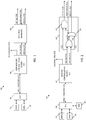
FIG. 1 is a block diagram of a first embodiment of a memory circuit including error correction in accordance with this disclosure; and -
FIG. 2 is a block diagram of a second embodiment of a memory circuit including error correction in accordance with this disclosure. - When introducing elements of various embodiments of the present disclosure, the articles "a," "an," and "the" are intended to mean that there are one or more of the elements. The terms "comprising," "including," and "having" are intended to be inclusive and mean that there may be additional elements other than the listed elements. Additionally, it should be understood that references to "one embodiment" or "an embodiment" of the present disclosure are not intended to be interpreted as excluding the existence of additional embodiments that also incorporate the recited features. Like reference numbers in the drawing figures refer to like elements throughout, and prime notation is used to indicate similar structures in different embodiments.
- A first embodiment of a
memory architecture 50 including error correction is now described with reference toFIG. 1 . Thememory architecture 50 includes first and second double data rate (DDR) synchronous dynamic random-access memory (SDRAM), designated asDDRO 52 andDDR1 54, and each coupled to a physical interface (PHY) 56. Thephysical interface 56 is coupled to amemory controller 58 with an error correcting circuit incorporated therein or associated therewith. Thephysical interface 56 is a double data rate synchronous dynamic random-access memory interface so to enable proper communication withDDRO 52 andDDR1 54, and the error checking performed is of the Hamming type with an additional parity bit, referred to as SECDED (i.e. single error correction, double error detection). - The minimum distance of this SECDED error correction is four, which is to say that the minimum number of positions in which any two distinct codewords differ is four. This allows the error correction to distinguish between single bit errors and two-bit errors in a given packet. Thus, a single error can be detected and corrected while at the same time detecting (but not correcting) a double error. SECDED detection is known to those of skill in the art and therefore the details thereof need not be described herein.
- The
physical interface 56 sends data packets comprised of data bits and checkbits 51 to thememory controller 58, which performs the aforementioned error correction. Thememory controller 58 determines whether a correctable error (single bit error) is present in a received data packet and generates aSEC Int signal 55 indicating as such, as output. Thememory controller 58 also determines whether an uncorrectable error (two-bit error) is present in the received data packet and generates a DED Int signal 57 indicating as such, as output. If a correctable error was detected, then a new packet containing correctedbits 53 is generated and output by thememory controller 58. - A
response manager 60 receives theSEC Int signal 55 and theDED Int signal 57. If the operating conditions of thememory architecture 50 are such that where there is the occurrence of faults in the data packet within the reliable operation limits of the provided SECDED error correction (i.e. there is possibility of only one or two-bit faults), theresponse manager 60 operates in an availability mode, allowing the correction of one-bit faults and the detection of two-bit faults, and passing theSEC Int signal 55 and DED Int signal 57 as theSEC Ext signal 59 and theDED Ext Signal 63 as outputs, respectively. This availability mode is so called because the error correction and possibility of only one-bit and two-bit faults leads to a high availability of thememory architecture 50. - However, if the operating conditions of the memory architecture are such that there is a high presence of noise, and possible fault conditions include more bit faults than the limit of correction and detection provided by the SECDED (e.g. three or more bit errors), the
response manager 60 operates in a coverage mode in which a correctable fault indication is treated as an uncorrectable error, since a three-bit or greater error, which is not correctable, may be detected by SECDED as a single-bit correctable error. Therefore, in the coverage mode, if theSEC Int signal 55 indicates potential presence of a single-bit correctable error (potential since this may actually be incorrect and instead represent presence of a three-bit or higher uncorrectable error), or if theDED Int signal 57 indicates presence of a double-bit uncorrectable error, theDED Ext signal 63 is asserted to indicate the potential presence of uncorrectable errors, while theSEC Ext signal 59 is not asserted. The coverage mode is so called because this operation reduces availability of the system, but reliably detects the presence of faults, therefore enhancing the fault detection coverage provided by the system. - The selection between the availability mode and the coverage mode may be made by the
response manager 60, or by an external entity. This selection may be made based upon information about the operating conditions of thememory architecture 50, which may be received from external sources such as sensors, or a microprocessor or system-on-a-chip in communication with such sensors. The operating conditions may include temperature, background electromagnetic radiation, or any other operating conditions of concern. This selection may additionally or alternatively be made based upon configuration provided by external entity, such as a microprocessor or system-on-a-chip, or provided during device fabrication. - Still further, this selection may additionally or alternatively be made on a packet by packet basis based upon which specific memory sent the data packet. For example, the
memory architecture 50 may include a DDR memory and a non-DDR memory, and coverage mode may be activated when data is to be received from the DDR memory, while availability mode may be activated when data is to be received from the non-DDR memory. Such an embodiment is illustrated inFIG. 2 , in which DDR memories DDRO 52 andDDR1 54, as well as anon-DDR RAM 49, are coupled to thephysical interface 56. - As explained above, the advantage of the
memory architecture 50 including the response manager is that SECDED may indicate the presence of a single-bit correctable error and a lack of presence of a double-bit uncorrectable error when, in reality, a three-bit or greater error is present, but may now be used in coverage mode to reliably detect three-bit or greater errors. This is particularly useful in applications where DDR RAM is employed, as DDR RAM is prone to high fault rates (e.g. three-bit or greater errors). Moreover, accurate error detection of three-bit or greater errors allows for the expansion of the use of DDR RAM (and its high throughput rate) into applications in which it is not conventionally used, such as safety and automotive applications. - One specific architecture for the response manager 60' is now described with reference to
FIG. 2 . Here, the response manager 60' includes anOR gate 62 that receives theSEC Int signal 55 andDED Int signal 57, and generatesoutput 65 based thereupon. Amultiplexer 64 receives theoutput 65 from theOR gate 62 as input, as well as theDED Int signal 57. Themultiplexer 64 is controlled by a received modeselect signal 61 that indicates whether availability mode or coverage mode is to be used. Themultiplexer 64 generates theDED Ext signal 63. An ANDgate 66 receives as input theSEC Int signal 55, as well as the modeselect signal 61. The ANDgate 66 generates theSEC Int signal 59. - It should be appreciated, however, that other architectures may be used for the response manager 60'. It should also be appreciated that while the memory architectures herein have been described with respect to the error correction used being SECDED, the principles herein may be applied to architectures using different kinds of error correction.
- While the disclosure has been described with respect to a limited number of embodiments, those skilled in the art, having benefit of this disclosure, will appreciate that other embodiments can be envisioned and modifications may be made to the electronic device and method described and illustrated herein, without thereby departing from the scope of the present invention, as defined in the attached claims.
Claims (17)
- An electronic device (50), comprising:error correction circuitry (58) configured to;receive a data packet (51);determine whether a correctable error is present in the data packet, and output a correctable error flag (55) indicating presence or absence of the correctable error in the data packet;determine whether an uncorrectable error is present in the data packet, and output an uncorrectable error flag (57) indicating presence or absence of the uncorrectable error in the data packet;a response manager circuit (60; 60') configured to receive the correctable error flag and the uncorrectable flag, and:in an availability mode, generate an output indicating that a correctable error was present in the data packet if the correctable error flag indicates presence of the correctable error in the data packet, and generate an output indicating that an uncorrectable error was present in the data packet if the uncorrectable error flag indicates presence of the uncorrectable error in the data packet; andin a coverage mode, generate an output indicating that a correctable error was potentially present in the data packet but should be treated as an uncorrectable error if the correctable error flag indicates presence of the correctable error in the data packet, and generate an output indicating that an uncorrectable error was present in the data packet if the uncorrectable error flag indicates presence of the uncorrectable error in the data packet.
- The circuit of claim 1, wherein the response manager circuit (60') comprises:an OR gate (62) receiving the correctable error flag ((55)) and the uncorrectable error flag ((57)) as inputs, and generating output (65);an AND gate (66) receiving the correctable error flag and a mode select signal (61) as inputs, and generating a first output (59); anda multiplexer (64) receiving the uncorrectable error flag and the output (65) of the OR gate as input, and generating a second output (63) in response to the mode select signal.
- The circuit of claim 1 or 2, wherein the response manager circuit (60) determines whether to enter availability mode or coverage mode as a function of at least one received operating condition of the circuit.
- The circuit of any of claims 1 to 3, wherein the response manager circuit (60; 60') determines whether to enter availability mode or coverage mode as a function of a received configuration profile.
- The circuit of any of claims 1 to 4, further comprising:a first memory (52; 54) having a first memory type;a second memory (49) having a second memory type different than the first memory type;physical interface circuitry (56) coupling the first memory and the second memory to the error correction circuitry (58);wherein the response manager circuit (60; 60') determines whether to enter availability mode or coverage mode based upon whether the data packet was received from the first memory or the second memory.
- The circuit of claim 5, wherein the first memory type is a less reliable memory type than the second memory type such that an error in transmission of data from the first memory (52; 54) is more likely than an error in transmission of data from the second memory (49).
- The circuit of claim 6, wherein the first memory type is double data rate synchronous dynamic random-access memory (52; 54).
- The circuit of any of claims 1 to 7, wherein the error correction circuitry comprises Hamming error correction circuitry.
- An electronic device (50), comprising:error correction circuitry (58) configured to:receive a data packet (51);determine whether a correctable error is present in the data packet, and output a correctable error flag ((55)) indicating presence or absence of the correctable error in the data packet;determine whether an uncorrectable error is present in the data packet, and output an uncorrectable error flag ((57)) indicating presence or absence of the uncorrectable error in the data packet;a response manager circuit (60) comprising:an OR gate (62) receiving the correctable error flag and uncorrectable error flag as inputs, and generating an output (65);an AND gate (66) receiving the correctable error flag and a mode select signal (61) as inputs, and generating a first output (59); anda multiplexer (64) receiving the uncorrectable error flag and the output (65) of the OR gate as input, and generating a second output (63) in response to the mode select signal.
- The circuit of claim 9, wherein, when the mode select signal (61) indicates that the response manager circuit (60) is to operate in an availability mode, the first output (59) indicates that a correctable error was present in the data packet (51) if the correctable error flag indicates presence of the correctable error in the data packet, and the second output (63) indicates that an uncorrectable error was present in the data packet if the uncorrectable error flag indicates presence of the uncorrectable error in the data packet.
- The circuit of claim 9, wherein, when the mode select signal (61) indicates that the response manager circuit (60) is to operate in a coverage mode, the first output (59) indicates that a correctable error was potentially present in the data packet (51) but should be treated as an uncorrectable error if the correctable error flag indicates presence of the correctable error in the data packet, and the second output indicates that an uncorrectable error was present in the data packet (63) if the uncorrectable error flag indicates presence of the uncorrectable error in the data packet.
- A method of operating an electronic device, comprising:a) receiving a data packet;b) determining whether a correctable error is present in the data packet;c) determining whether an uncorrectable error is present in the data packet;d) determining whether to enter coverage mode or availability mode;e) in the availability mode, indicating that a correctable error was present in the data packet, and generate an output indicating that an uncorrectable error was present in the data packet if an uncorrectable error was in the data packet; andf) in the coverage mode, indicating that a correctable error was potentially present in the data packet but should be treated as an uncorrectable error a correctable error was present in the data packet, and generate an output indicating that an uncorrectable error was present in the data packet if an uncorrectable error was present in the data packet.
- The method of claim 12, wherein whether to enter availability mode or coverage mode is determined as a function of at least one received operating condition of the electronic device.
- The method of claim 12, wherein whether to enter availability mode or coverage mode is determined as a function of a received configuration profile.
- The method of claim 12, wherein whether to enter availability mode or coverage mode is determined based upon whether the data packet was received from a first memory or a second memory.
- The method of claim 51, wherein the first memory type is a less reliable memory type than the second memory type such that an error in transmission of data from the first memory is more likely than an error in transmission of data from the second memory.
- The method of any of claims 12 to 16, wherein a), b), and c) are performed using Hamming error correction.
Applications Claiming Priority (1)
| Application Number | Priority Date | Filing Date | Title |
|---|---|---|---|
| US15/798,916 US10379937B2 (en) | 2017-10-31 | 2017-10-31 | Memory architecture including response manager for error correction circuit |
Publications (2)
| Publication Number | Publication Date |
|---|---|
| EP3477478A1 true EP3477478A1 (en) | 2019-05-01 |
| EP3477478B1 EP3477478B1 (en) | 2022-11-30 |
Family
ID=63965250
Family Applications (1)
| Application Number | Title | Priority Date | Filing Date |
|---|---|---|---|
| EP18201756.6A Active EP3477478B1 (en) | 2017-10-31 | 2018-10-22 | Memory architecture including response manager for error correction circuit |
Country Status (3)
| Country | Link |
|---|---|
| US (2) | US10379937B2 (en) |
| EP (1) | EP3477478B1 (en) |
| CN (3) | CN109726030B (en) |
Families Citing this family (3)
| Publication number | Priority date | Publication date | Assignee | Title |
|---|---|---|---|---|
| US10379937B2 (en) * | 2017-10-31 | 2019-08-13 | Stmicroelectronics International N.V. | Memory architecture including response manager for error correction circuit |
| US11429527B2 (en) * | 2018-10-15 | 2022-08-30 | Texas Instruments Incorporated | Adaptive credit-based replenishment threshold used for transaction arbitration in a system that supports multiple levels of credit expenditure |
| US11121820B2 (en) * | 2019-11-12 | 2021-09-14 | Qualcomm Incorporated | Media access controller with a codec error model |
Citations (3)
| Publication number | Priority date | Publication date | Assignee | Title |
|---|---|---|---|---|
| EP2256634A1 (en) * | 2009-05-27 | 2010-12-01 | Robert Bosch Gmbh | A data processing device and a method for error detection and error correction |
| US20140189427A1 (en) * | 2012-12-28 | 2014-07-03 | Prahladachar Jayaprakash Bharadwaj | Live error recovery |
| US20140380132A1 (en) * | 2013-06-25 | 2014-12-25 | Adee O. Ran | Increasing communication safety by preventing false packet acceptance in high-speed links |
Family Cites Families (9)
| Publication number | Priority date | Publication date | Assignee | Title |
|---|---|---|---|---|
| US5247523A (en) * | 1989-07-12 | 1993-09-21 | Hitachi, Ltd. | Code error correction apparatus |
| US5978953A (en) * | 1996-12-19 | 1999-11-02 | Compaq Computer Corporation | error detection and correction |
| US6216247B1 (en) * | 1998-05-29 | 2001-04-10 | Intel Corporation | 32-bit mode for a 64-bit ECC capable memory subsystem |
| US7587658B1 (en) * | 2005-01-03 | 2009-09-08 | Sun Microsystems, Inc. | ECC encoding for uncorrectable errors |
| US7502986B2 (en) * | 2005-02-09 | 2009-03-10 | International Business Machines Corporation | Method and apparatus for collecting failure information on error correction code (ECC) protected data |
| US8812898B1 (en) * | 2012-09-27 | 2014-08-19 | Cadence Design Systems, Inc. | System and method for transfer of data between memory with dynamic error recovery |
| JP6275427B2 (en) * | 2013-09-06 | 2018-02-07 | 株式会社東芝 | Memory control circuit and cache memory |
| KR102435181B1 (en) * | 2015-11-16 | 2022-08-23 | 삼성전자주식회사 | Semiconductor memory device, memory system including the same and method of operating memory system |
| US10379937B2 (en) * | 2017-10-31 | 2019-08-13 | Stmicroelectronics International N.V. | Memory architecture including response manager for error correction circuit |
-
2017
- 2017-10-31 US US15/798,916 patent/US10379937B2/en active Active
-
2018
- 2018-10-22 EP EP18201756.6A patent/EP3477478B1/en active Active
- 2018-10-30 CN CN201811277573.3A patent/CN109726030B/en active Active
- 2018-10-30 CN CN202310039589.5A patent/CN115964215A/en active Pending
- 2018-10-30 CN CN201821770591.0U patent/CN209105195U/en not_active Withdrawn - After Issue
-
2019
- 2019-06-27 US US16/454,365 patent/US10860415B2/en active Active
Patent Citations (3)
| Publication number | Priority date | Publication date | Assignee | Title |
|---|---|---|---|---|
| EP2256634A1 (en) * | 2009-05-27 | 2010-12-01 | Robert Bosch Gmbh | A data processing device and a method for error detection and error correction |
| US20140189427A1 (en) * | 2012-12-28 | 2014-07-03 | Prahladachar Jayaprakash Bharadwaj | Live error recovery |
| US20140380132A1 (en) * | 2013-06-25 | 2014-12-25 | Adee O. Ran | Increasing communication safety by preventing false packet acceptance in high-speed links |
Also Published As
| Publication number | Publication date |
|---|---|
| US20190317851A1 (en) | 2019-10-17 |
| US10860415B2 (en) | 2020-12-08 |
| US10379937B2 (en) | 2019-08-13 |
| CN209105195U (en) | 2019-07-12 |
| CN109726030B (en) | 2023-02-10 |
| EP3477478B1 (en) | 2022-11-30 |
| CN109726030A (en) | 2019-05-07 |
| CN115964215A (en) | 2023-04-14 |
| US20190129790A1 (en) | 2019-05-02 |
Similar Documents
| Publication | Publication Date | Title |
|---|---|---|
| US7073117B1 (en) | Method and apparatus for generating bit errors in a forward error correction (FEC) system to estimate power dissipation characteristics of the system | |
| US6799287B1 (en) | Method and apparatus for verifying error correcting codes | |
| US7137057B2 (en) | Method and apparatus for performing error correction code (ECC) conversion | |
| US20110154154A1 (en) | Signal segmentation method and crc attachment method for reducing undetected error | |
| US3646518A (en) | Feedback error control system | |
| US8694872B2 (en) | Extended bidirectional hamming code for double-error correction and triple-error detection | |
| WO2000073907A1 (en) | System and method for protecting data and correcting bit errors due to component failures | |
| US10860415B2 (en) | Memory architecture including response manager for error correction circuit | |
| CA2274106C (en) | Shortened fire code error-trapping decoding method and apparatus | |
| US9934841B1 (en) | Systems and methods for refreshing data in memory circuits | |
| US20080155372A1 (en) | Methods and apparatus for improving error indication performance in systems with low-density parity check codes | |
| US6981200B2 (en) | Interconnect system with error correction | |
| JP2970994B2 (en) | Error correction decoding circuit | |
| US8910009B1 (en) | Method and apparatus for enhancing error detection in data transmission | |
| Sokolovskyi et al. | DEVELOPMENT OF THE METHOD OF DETECTING AND CORRECTING DATA TRANSMISSION ERRORS IN IOT SYSTEMS FOR MONITORING THE STATE OF OBJECTS. | |
| US9515682B2 (en) | Device for correcting two errors with a code of hamming distance three or four | |
| CN116954981A (en) | Method for storing data, method for reading data and related equipment | |
| CN116527062A (en) | Test device and method for verifying RS (Reed-Solomon) encoding and decoding circuit function | |
| US7096414B2 (en) | In-line wire error correction | |
| KR100292788B1 (en) | Error Detection and Correction Circuit | |
| Singh et al. | Improving performance parameters of error detection and correction in hdlc protocol by using hamming method | |
| US20240395346A1 (en) | Data correcting device and data correcting method thereof | |
| Faraj | Design error detection and correction system based on Reed-Muller matrix for memory protection | |
| KR100407131B1 (en) | Reed solomon decoder using combinational circuits | |
| JPH05197580A (en) | Two-bit error correction circuit |
Legal Events
| Date | Code | Title | Description |
|---|---|---|---|
| PUAI | Public reference made under article 153(3) epc to a published international application that has entered the european phase |
Free format text: ORIGINAL CODE: 0009012 |
|
| STAA | Information on the status of an ep patent application or granted ep patent |
Free format text: STATUS: THE APPLICATION HAS BEEN PUBLISHED |
|
| AK | Designated contracting states |
Kind code of ref document: A1 Designated state(s): AL AT BE BG CH CY CZ DE DK EE ES FI FR GB GR HR HU IE IS IT LI LT LU LV MC MK MT NL NO PL PT RO RS SE SI SK SM TR |
|
| AX | Request for extension of the european patent |
Extension state: BA ME |
|
| STAA | Information on the status of an ep patent application or granted ep patent |
Free format text: STATUS: REQUEST FOR EXAMINATION WAS MADE |
|
| 17P | Request for examination filed |
Effective date: 20191030 |
|
| RBV | Designated contracting states (corrected) |
Designated state(s): AL AT BE BG CH CY CZ DE DK EE ES FI FR GB GR HR HU IE IS IT LI LT LU LV MC MK MT NL NO PL PT RO RS SE SI SK SM TR |
|
| STAA | Information on the status of an ep patent application or granted ep patent |
Free format text: STATUS: EXAMINATION IS IN PROGRESS |
|
| 17Q | First examination report despatched |
Effective date: 20200212 |
|
| GRAP | Despatch of communication of intention to grant a patent |
Free format text: ORIGINAL CODE: EPIDOSNIGR1 |
|
| STAA | Information on the status of an ep patent application or granted ep patent |
Free format text: STATUS: GRANT OF PATENT IS INTENDED |
|
| INTG | Intention to grant announced |
Effective date: 20220610 |
|
| GRAS | Grant fee paid |
Free format text: ORIGINAL CODE: EPIDOSNIGR3 |
|
| GRAA | (expected) grant |
Free format text: ORIGINAL CODE: 0009210 |
|
| STAA | Information on the status of an ep patent application or granted ep patent |
Free format text: STATUS: THE PATENT HAS BEEN GRANTED |
|
| AK | Designated contracting states |
Kind code of ref document: B1 Designated state(s): AL AT BE BG CH CY CZ DE DK EE ES FI FR GB GR HR HU IE IS IT LI LT LU LV MC MK MT NL NO PL PT RO RS SE SI SK SM TR |
|
| REG | Reference to a national code |
Ref country code: CH Ref legal event code: EP Ref country code: GB Ref legal event code: FG4D |
|
| REG | Reference to a national code |
Ref country code: AT Ref legal event code: REF Ref document number: 1535205 Country of ref document: AT Kind code of ref document: T Effective date: 20221215 |
|
| REG | Reference to a national code |
Ref country code: IE Ref legal event code: FG4D |
|
| REG | Reference to a national code |
Ref country code: DE Ref legal event code: R096 Ref document number: 602018043585 Country of ref document: DE |
|
| REG | Reference to a national code |
Ref country code: LT Ref legal event code: MG9D |
|
| REG | Reference to a national code |
Ref country code: NL Ref legal event code: MP Effective date: 20221130 |
|
| PG25 | Lapsed in a contracting state [announced via postgrant information from national office to epo] |
Ref country code: SE Free format text: LAPSE BECAUSE OF FAILURE TO SUBMIT A TRANSLATION OF THE DESCRIPTION OR TO PAY THE FEE WITHIN THE PRESCRIBED TIME-LIMIT Effective date: 20221130 Ref country code: PT Free format text: LAPSE BECAUSE OF FAILURE TO SUBMIT A TRANSLATION OF THE DESCRIPTION OR TO PAY THE FEE WITHIN THE PRESCRIBED TIME-LIMIT Effective date: 20230331 Ref country code: NO Free format text: LAPSE BECAUSE OF FAILURE TO SUBMIT A TRANSLATION OF THE DESCRIPTION OR TO PAY THE FEE WITHIN THE PRESCRIBED TIME-LIMIT Effective date: 20230228 Ref country code: LT Free format text: LAPSE BECAUSE OF FAILURE TO SUBMIT A TRANSLATION OF THE DESCRIPTION OR TO PAY THE FEE WITHIN THE PRESCRIBED TIME-LIMIT Effective date: 20221130 Ref country code: FI Free format text: LAPSE BECAUSE OF FAILURE TO SUBMIT A TRANSLATION OF THE DESCRIPTION OR TO PAY THE FEE WITHIN THE PRESCRIBED TIME-LIMIT Effective date: 20221130 Ref country code: ES Free format text: LAPSE BECAUSE OF FAILURE TO SUBMIT A TRANSLATION OF THE DESCRIPTION OR TO PAY THE FEE WITHIN THE PRESCRIBED TIME-LIMIT Effective date: 20221130 |
|
| REG | Reference to a national code |
Ref country code: AT Ref legal event code: MK05 Ref document number: 1535205 Country of ref document: AT Kind code of ref document: T Effective date: 20221130 |
|
| PG25 | Lapsed in a contracting state [announced via postgrant information from national office to epo] |
Ref country code: RS Free format text: LAPSE BECAUSE OF FAILURE TO SUBMIT A TRANSLATION OF THE DESCRIPTION OR TO PAY THE FEE WITHIN THE PRESCRIBED TIME-LIMIT Effective date: 20221130 Ref country code: PL Free format text: LAPSE BECAUSE OF FAILURE TO SUBMIT A TRANSLATION OF THE DESCRIPTION OR TO PAY THE FEE WITHIN THE PRESCRIBED TIME-LIMIT Effective date: 20221130 Ref country code: LV Free format text: LAPSE BECAUSE OF FAILURE TO SUBMIT A TRANSLATION OF THE DESCRIPTION OR TO PAY THE FEE WITHIN THE PRESCRIBED TIME-LIMIT Effective date: 20221130 Ref country code: IS Free format text: LAPSE BECAUSE OF FAILURE TO SUBMIT A TRANSLATION OF THE DESCRIPTION OR TO PAY THE FEE WITHIN THE PRESCRIBED TIME-LIMIT Effective date: 20230330 Ref country code: HR Free format text: LAPSE BECAUSE OF FAILURE TO SUBMIT A TRANSLATION OF THE DESCRIPTION OR TO PAY THE FEE WITHIN THE PRESCRIBED TIME-LIMIT Effective date: 20221130 Ref country code: GR Free format text: LAPSE BECAUSE OF FAILURE TO SUBMIT A TRANSLATION OF THE DESCRIPTION OR TO PAY THE FEE WITHIN THE PRESCRIBED TIME-LIMIT Effective date: 20230301 |
|
| PG25 | Lapsed in a contracting state [announced via postgrant information from national office to epo] |
Ref country code: NL Free format text: LAPSE BECAUSE OF FAILURE TO SUBMIT A TRANSLATION OF THE DESCRIPTION OR TO PAY THE FEE WITHIN THE PRESCRIBED TIME-LIMIT Effective date: 20221130 |
|
| PG25 | Lapsed in a contracting state [announced via postgrant information from national office to epo] |
Ref country code: SM Free format text: LAPSE BECAUSE OF FAILURE TO SUBMIT A TRANSLATION OF THE DESCRIPTION OR TO PAY THE FEE WITHIN THE PRESCRIBED TIME-LIMIT Effective date: 20221130 Ref country code: RO Free format text: LAPSE BECAUSE OF FAILURE TO SUBMIT A TRANSLATION OF THE DESCRIPTION OR TO PAY THE FEE WITHIN THE PRESCRIBED TIME-LIMIT Effective date: 20221130 Ref country code: EE Free format text: LAPSE BECAUSE OF FAILURE TO SUBMIT A TRANSLATION OF THE DESCRIPTION OR TO PAY THE FEE WITHIN THE PRESCRIBED TIME-LIMIT Effective date: 20221130 Ref country code: DK Free format text: LAPSE BECAUSE OF FAILURE TO SUBMIT A TRANSLATION OF THE DESCRIPTION OR TO PAY THE FEE WITHIN THE PRESCRIBED TIME-LIMIT Effective date: 20221130 Ref country code: CZ Free format text: LAPSE BECAUSE OF FAILURE TO SUBMIT A TRANSLATION OF THE DESCRIPTION OR TO PAY THE FEE WITHIN THE PRESCRIBED TIME-LIMIT Effective date: 20221130 Ref country code: AT Free format text: LAPSE BECAUSE OF FAILURE TO SUBMIT A TRANSLATION OF THE DESCRIPTION OR TO PAY THE FEE WITHIN THE PRESCRIBED TIME-LIMIT Effective date: 20221130 |
|
| PG25 | Lapsed in a contracting state [announced via postgrant information from national office to epo] |
Ref country code: SK Free format text: LAPSE BECAUSE OF FAILURE TO SUBMIT A TRANSLATION OF THE DESCRIPTION OR TO PAY THE FEE WITHIN THE PRESCRIBED TIME-LIMIT Effective date: 20221130 Ref country code: AL Free format text: LAPSE BECAUSE OF FAILURE TO SUBMIT A TRANSLATION OF THE DESCRIPTION OR TO PAY THE FEE WITHIN THE PRESCRIBED TIME-LIMIT Effective date: 20221130 |
|
| REG | Reference to a national code |
Ref country code: DE Ref legal event code: R097 Ref document number: 602018043585 Country of ref document: DE |
|
| PLBE | No opposition filed within time limit |
Free format text: ORIGINAL CODE: 0009261 |
|
| STAA | Information on the status of an ep patent application or granted ep patent |
Free format text: STATUS: NO OPPOSITION FILED WITHIN TIME LIMIT |
|
| 26N | No opposition filed |
Effective date: 20230831 |
|
| PG25 | Lapsed in a contracting state [announced via postgrant information from national office to epo] |
Ref country code: SI Free format text: LAPSE BECAUSE OF FAILURE TO SUBMIT A TRANSLATION OF THE DESCRIPTION OR TO PAY THE FEE WITHIN THE PRESCRIBED TIME-LIMIT Effective date: 20221130 |
|
| PG25 | Lapsed in a contracting state [announced via postgrant information from national office to epo] |
Ref country code: IT Free format text: LAPSE BECAUSE OF FAILURE TO SUBMIT A TRANSLATION OF THE DESCRIPTION OR TO PAY THE FEE WITHIN THE PRESCRIBED TIME-LIMIT Effective date: 20221130 Ref country code: MC Free format text: LAPSE BECAUSE OF FAILURE TO SUBMIT A TRANSLATION OF THE DESCRIPTION OR TO PAY THE FEE WITHIN THE PRESCRIBED TIME-LIMIT Effective date: 20221130 |
|
| REG | Reference to a national code |
Ref country code: CH Ref legal event code: PL |
|
| REG | Reference to a national code |
Ref country code: BE Ref legal event code: MM Effective date: 20231031 |
|
| PG25 | Lapsed in a contracting state [announced via postgrant information from national office to epo] |
Ref country code: LU Free format text: LAPSE BECAUSE OF NON-PAYMENT OF DUE FEES Effective date: 20231022 |
|
| GBPC | Gb: european patent ceased through non-payment of renewal fee |
Effective date: 20231022 |
|
| PG25 | Lapsed in a contracting state [announced via postgrant information from national office to epo] |
Ref country code: LU Free format text: LAPSE BECAUSE OF NON-PAYMENT OF DUE FEES Effective date: 20231022 |
|
| PG25 | Lapsed in a contracting state [announced via postgrant information from national office to epo] |
Ref country code: GB Free format text: LAPSE BECAUSE OF NON-PAYMENT OF DUE FEES Effective date: 20231022 |
|
| PG25 | Lapsed in a contracting state [announced via postgrant information from national office to epo] |
Ref country code: CH Free format text: LAPSE BECAUSE OF NON-PAYMENT OF DUE FEES Effective date: 20231031 |
|
| PG25 | Lapsed in a contracting state [announced via postgrant information from national office to epo] |
Ref country code: GB Free format text: LAPSE BECAUSE OF NON-PAYMENT OF DUE FEES Effective date: 20231022 Ref country code: FR Free format text: LAPSE BECAUSE OF NON-PAYMENT OF DUE FEES Effective date: 20231031 Ref country code: CH Free format text: LAPSE BECAUSE OF NON-PAYMENT OF DUE FEES Effective date: 20231031 |
|
| PG25 | Lapsed in a contracting state [announced via postgrant information from national office to epo] |
Ref country code: BE Free format text: LAPSE BECAUSE OF NON-PAYMENT OF DUE FEES Effective date: 20231031 |
|
| PG25 | Lapsed in a contracting state [announced via postgrant information from national office to epo] |
Ref country code: IE Free format text: LAPSE BECAUSE OF NON-PAYMENT OF DUE FEES Effective date: 20231022 |
|
| PG25 | Lapsed in a contracting state [announced via postgrant information from national office to epo] |
Ref country code: IE Free format text: LAPSE BECAUSE OF NON-PAYMENT OF DUE FEES Effective date: 20231022 |
|
| PG25 | Lapsed in a contracting state [announced via postgrant information from national office to epo] |
Ref country code: BG Free format text: LAPSE BECAUSE OF FAILURE TO SUBMIT A TRANSLATION OF THE DESCRIPTION OR TO PAY THE FEE WITHIN THE PRESCRIBED TIME-LIMIT Effective date: 20221130 |
|
| PG25 | Lapsed in a contracting state [announced via postgrant information from national office to epo] |
Ref country code: BG Free format text: LAPSE BECAUSE OF FAILURE TO SUBMIT A TRANSLATION OF THE DESCRIPTION OR TO PAY THE FEE WITHIN THE PRESCRIBED TIME-LIMIT Effective date: 20221130 |
|
| PG25 | Lapsed in a contracting state [announced via postgrant information from national office to epo] |
Ref country code: CY Free format text: LAPSE BECAUSE OF FAILURE TO SUBMIT A TRANSLATION OF THE DESCRIPTION OR TO PAY THE FEE WITHIN THE PRESCRIBED TIME-LIMIT; INVALID AB INITIO Effective date: 20181022 |
|
| PG25 | Lapsed in a contracting state [announced via postgrant information from national office to epo] |
Ref country code: HU Free format text: LAPSE BECAUSE OF FAILURE TO SUBMIT A TRANSLATION OF THE DESCRIPTION OR TO PAY THE FEE WITHIN THE PRESCRIBED TIME-LIMIT; INVALID AB INITIO Effective date: 20181022 |
|
| PG25 | Lapsed in a contracting state [announced via postgrant information from national office to epo] |
Ref country code: TR Free format text: LAPSE BECAUSE OF FAILURE TO SUBMIT A TRANSLATION OF THE DESCRIPTION OR TO PAY THE FEE WITHIN THE PRESCRIBED TIME-LIMIT Effective date: 20221130 |
|
| PGFP | Annual fee paid to national office [announced via postgrant information from national office to epo] |
Ref country code: DE Payment date: 20250923 Year of fee payment: 8 |