EP3477371A1 - Liquid crystal display pixel structure and liquid crystal display device - Google Patents
Liquid crystal display pixel structure and liquid crystal display device Download PDFInfo
- Publication number
- EP3477371A1 EP3477371A1 EP16905938.3A EP16905938A EP3477371A1 EP 3477371 A1 EP3477371 A1 EP 3477371A1 EP 16905938 A EP16905938 A EP 16905938A EP 3477371 A1 EP3477371 A1 EP 3477371A1
- Authority
- EP
- European Patent Office
- Prior art keywords
- display
- domain
- pixel
- display domain
- liquid crystal
- Prior art date
- Legal status (The legal status is an assumption and is not a legal conclusion. Google has not performed a legal analysis and makes no representation as to the accuracy of the status listed.)
- Granted
Links
Images


Classifications
-
- G—PHYSICS
- G02—OPTICS
- G02F—OPTICAL DEVICES OR ARRANGEMENTS FOR THE CONTROL OF LIGHT BY MODIFICATION OF THE OPTICAL PROPERTIES OF THE MEDIA OF THE ELEMENTS INVOLVED THEREIN; NON-LINEAR OPTICS; FREQUENCY-CHANGING OF LIGHT; OPTICAL LOGIC ELEMENTS; OPTICAL ANALOGUE/DIGITAL CONVERTERS
- G02F1/00—Devices or arrangements for the control of the intensity, colour, phase, polarisation or direction of light arriving from an independent light source, e.g. switching, gating or modulating; Non-linear optics
- G02F1/01—Devices or arrangements for the control of the intensity, colour, phase, polarisation or direction of light arriving from an independent light source, e.g. switching, gating or modulating; Non-linear optics for the control of the intensity, phase, polarisation or colour
- G02F1/13—Devices or arrangements for the control of the intensity, colour, phase, polarisation or direction of light arriving from an independent light source, e.g. switching, gating or modulating; Non-linear optics for the control of the intensity, phase, polarisation or colour based on liquid crystals, e.g. single liquid crystal display cells
- G02F1/133—Constructional arrangements; Operation of liquid crystal cells; Circuit arrangements
- G02F1/136—Liquid crystal cells structurally associated with a semi-conducting layer or substrate, e.g. cells forming part of an integrated circuit
- G02F1/1362—Active matrix addressed cells
- G02F1/136286—Wiring, e.g. gate line, drain line
-
- G—PHYSICS
- G02—OPTICS
- G02F—OPTICAL DEVICES OR ARRANGEMENTS FOR THE CONTROL OF LIGHT BY MODIFICATION OF THE OPTICAL PROPERTIES OF THE MEDIA OF THE ELEMENTS INVOLVED THEREIN; NON-LINEAR OPTICS; FREQUENCY-CHANGING OF LIGHT; OPTICAL LOGIC ELEMENTS; OPTICAL ANALOGUE/DIGITAL CONVERTERS
- G02F1/00—Devices or arrangements for the control of the intensity, colour, phase, polarisation or direction of light arriving from an independent light source, e.g. switching, gating or modulating; Non-linear optics
- G02F1/01—Devices or arrangements for the control of the intensity, colour, phase, polarisation or direction of light arriving from an independent light source, e.g. switching, gating or modulating; Non-linear optics for the control of the intensity, phase, polarisation or colour
- G02F1/13—Devices or arrangements for the control of the intensity, colour, phase, polarisation or direction of light arriving from an independent light source, e.g. switching, gating or modulating; Non-linear optics for the control of the intensity, phase, polarisation or colour based on liquid crystals, e.g. single liquid crystal display cells
- G02F1/133—Constructional arrangements; Operation of liquid crystal cells; Circuit arrangements
- G02F1/1333—Constructional arrangements; Manufacturing methods
- G02F1/1337—Surface-induced orientation of the liquid crystal molecules, e.g. by alignment layers
- G02F1/133738—Surface-induced orientation of the liquid crystal molecules, e.g. by alignment layers for homogeneous alignment
-
- G—PHYSICS
- G02—OPTICS
- G02F—OPTICAL DEVICES OR ARRANGEMENTS FOR THE CONTROL OF LIGHT BY MODIFICATION OF THE OPTICAL PROPERTIES OF THE MEDIA OF THE ELEMENTS INVOLVED THEREIN; NON-LINEAR OPTICS; FREQUENCY-CHANGING OF LIGHT; OPTICAL LOGIC ELEMENTS; OPTICAL ANALOGUE/DIGITAL CONVERTERS
- G02F1/00—Devices or arrangements for the control of the intensity, colour, phase, polarisation or direction of light arriving from an independent light source, e.g. switching, gating or modulating; Non-linear optics
- G02F1/01—Devices or arrangements for the control of the intensity, colour, phase, polarisation or direction of light arriving from an independent light source, e.g. switching, gating or modulating; Non-linear optics for the control of the intensity, phase, polarisation or colour
- G02F1/13—Devices or arrangements for the control of the intensity, colour, phase, polarisation or direction of light arriving from an independent light source, e.g. switching, gating or modulating; Non-linear optics for the control of the intensity, phase, polarisation or colour based on liquid crystals, e.g. single liquid crystal display cells
- G02F1/133—Constructional arrangements; Operation of liquid crystal cells; Circuit arrangements
- G02F1/1333—Constructional arrangements; Manufacturing methods
- G02F1/1337—Surface-induced orientation of the liquid crystal molecules, e.g. by alignment layers
- G02F1/133753—Surface-induced orientation of the liquid crystal molecules, e.g. by alignment layers with different alignment orientations or pretilt angles on a same surface, e.g. for grey scale or improved viewing angle
-
- G—PHYSICS
- G02—OPTICS
- G02F—OPTICAL DEVICES OR ARRANGEMENTS FOR THE CONTROL OF LIGHT BY MODIFICATION OF THE OPTICAL PROPERTIES OF THE MEDIA OF THE ELEMENTS INVOLVED THEREIN; NON-LINEAR OPTICS; FREQUENCY-CHANGING OF LIGHT; OPTICAL LOGIC ELEMENTS; OPTICAL ANALOGUE/DIGITAL CONVERTERS
- G02F1/00—Devices or arrangements for the control of the intensity, colour, phase, polarisation or direction of light arriving from an independent light source, e.g. switching, gating or modulating; Non-linear optics
- G02F1/01—Devices or arrangements for the control of the intensity, colour, phase, polarisation or direction of light arriving from an independent light source, e.g. switching, gating or modulating; Non-linear optics for the control of the intensity, phase, polarisation or colour
- G02F1/13—Devices or arrangements for the control of the intensity, colour, phase, polarisation or direction of light arriving from an independent light source, e.g. switching, gating or modulating; Non-linear optics for the control of the intensity, phase, polarisation or colour based on liquid crystals, e.g. single liquid crystal display cells
- G02F1/133—Constructional arrangements; Operation of liquid crystal cells; Circuit arrangements
- G02F1/1333—Constructional arrangements; Manufacturing methods
- G02F1/1343—Electrodes
-
- G—PHYSICS
- G02—OPTICS
- G02F—OPTICAL DEVICES OR ARRANGEMENTS FOR THE CONTROL OF LIGHT BY MODIFICATION OF THE OPTICAL PROPERTIES OF THE MEDIA OF THE ELEMENTS INVOLVED THEREIN; NON-LINEAR OPTICS; FREQUENCY-CHANGING OF LIGHT; OPTICAL LOGIC ELEMENTS; OPTICAL ANALOGUE/DIGITAL CONVERTERS
- G02F1/00—Devices or arrangements for the control of the intensity, colour, phase, polarisation or direction of light arriving from an independent light source, e.g. switching, gating or modulating; Non-linear optics
- G02F1/01—Devices or arrangements for the control of the intensity, colour, phase, polarisation or direction of light arriving from an independent light source, e.g. switching, gating or modulating; Non-linear optics for the control of the intensity, phase, polarisation or colour
- G02F1/13—Devices or arrangements for the control of the intensity, colour, phase, polarisation or direction of light arriving from an independent light source, e.g. switching, gating or modulating; Non-linear optics for the control of the intensity, phase, polarisation or colour based on liquid crystals, e.g. single liquid crystal display cells
- G02F1/133—Constructional arrangements; Operation of liquid crystal cells; Circuit arrangements
- G02F1/1333—Constructional arrangements; Manufacturing methods
- G02F1/1343—Electrodes
- G02F1/134309—Electrodes characterised by their geometrical arrangement
-
- G—PHYSICS
- G02—OPTICS
- G02F—OPTICAL DEVICES OR ARRANGEMENTS FOR THE CONTROL OF LIGHT BY MODIFICATION OF THE OPTICAL PROPERTIES OF THE MEDIA OF THE ELEMENTS INVOLVED THEREIN; NON-LINEAR OPTICS; FREQUENCY-CHANGING OF LIGHT; OPTICAL LOGIC ELEMENTS; OPTICAL ANALOGUE/DIGITAL CONVERTERS
- G02F1/00—Devices or arrangements for the control of the intensity, colour, phase, polarisation or direction of light arriving from an independent light source, e.g. switching, gating or modulating; Non-linear optics
- G02F1/01—Devices or arrangements for the control of the intensity, colour, phase, polarisation or direction of light arriving from an independent light source, e.g. switching, gating or modulating; Non-linear optics for the control of the intensity, phase, polarisation or colour
- G02F1/13—Devices or arrangements for the control of the intensity, colour, phase, polarisation or direction of light arriving from an independent light source, e.g. switching, gating or modulating; Non-linear optics for the control of the intensity, phase, polarisation or colour based on liquid crystals, e.g. single liquid crystal display cells
- G02F1/133—Constructional arrangements; Operation of liquid crystal cells; Circuit arrangements
- G02F1/1333—Constructional arrangements; Manufacturing methods
- G02F1/1343—Electrodes
- G02F1/134309—Electrodes characterised by their geometrical arrangement
- G02F1/134345—Subdivided pixels, e.g. for grey scale or redundancy
-
- G—PHYSICS
- G02—OPTICS
- G02F—OPTICAL DEVICES OR ARRANGEMENTS FOR THE CONTROL OF LIGHT BY MODIFICATION OF THE OPTICAL PROPERTIES OF THE MEDIA OF THE ELEMENTS INVOLVED THEREIN; NON-LINEAR OPTICS; FREQUENCY-CHANGING OF LIGHT; OPTICAL LOGIC ELEMENTS; OPTICAL ANALOGUE/DIGITAL CONVERTERS
- G02F1/00—Devices or arrangements for the control of the intensity, colour, phase, polarisation or direction of light arriving from an independent light source, e.g. switching, gating or modulating; Non-linear optics
- G02F1/01—Devices or arrangements for the control of the intensity, colour, phase, polarisation or direction of light arriving from an independent light source, e.g. switching, gating or modulating; Non-linear optics for the control of the intensity, phase, polarisation or colour
- G02F1/13—Devices or arrangements for the control of the intensity, colour, phase, polarisation or direction of light arriving from an independent light source, e.g. switching, gating or modulating; Non-linear optics for the control of the intensity, phase, polarisation or colour based on liquid crystals, e.g. single liquid crystal display cells
- G02F1/133—Constructional arrangements; Operation of liquid crystal cells; Circuit arrangements
- G02F1/1333—Constructional arrangements; Manufacturing methods
- G02F1/1343—Electrodes
- G02F1/134309—Electrodes characterised by their geometrical arrangement
- G02F1/134363—Electrodes characterised by their geometrical arrangement for applying an electric field parallel to the substrate, i.e. in-plane switching [IPS]
-
- G—PHYSICS
- G02—OPTICS
- G02F—OPTICAL DEVICES OR ARRANGEMENTS FOR THE CONTROL OF LIGHT BY MODIFICATION OF THE OPTICAL PROPERTIES OF THE MEDIA OF THE ELEMENTS INVOLVED THEREIN; NON-LINEAR OPTICS; FREQUENCY-CHANGING OF LIGHT; OPTICAL LOGIC ELEMENTS; OPTICAL ANALOGUE/DIGITAL CONVERTERS
- G02F1/00—Devices or arrangements for the control of the intensity, colour, phase, polarisation or direction of light arriving from an independent light source, e.g. switching, gating or modulating; Non-linear optics
- G02F1/01—Devices or arrangements for the control of the intensity, colour, phase, polarisation or direction of light arriving from an independent light source, e.g. switching, gating or modulating; Non-linear optics for the control of the intensity, phase, polarisation or colour
- G02F1/13—Devices or arrangements for the control of the intensity, colour, phase, polarisation or direction of light arriving from an independent light source, e.g. switching, gating or modulating; Non-linear optics for the control of the intensity, phase, polarisation or colour based on liquid crystals, e.g. single liquid crystal display cells
- G02F1/133—Constructional arrangements; Operation of liquid crystal cells; Circuit arrangements
- G02F1/136—Liquid crystal cells structurally associated with a semi-conducting layer or substrate, e.g. cells forming part of an integrated circuit
- G02F1/1362—Active matrix addressed cells
- G02F1/1368—Active matrix addressed cells in which the switching element is a three-electrode device
-
- G—PHYSICS
- G02—OPTICS
- G02F—OPTICAL DEVICES OR ARRANGEMENTS FOR THE CONTROL OF LIGHT BY MODIFICATION OF THE OPTICAL PROPERTIES OF THE MEDIA OF THE ELEMENTS INVOLVED THEREIN; NON-LINEAR OPTICS; FREQUENCY-CHANGING OF LIGHT; OPTICAL LOGIC ELEMENTS; OPTICAL ANALOGUE/DIGITAL CONVERTERS
- G02F1/00—Devices or arrangements for the control of the intensity, colour, phase, polarisation or direction of light arriving from an independent light source, e.g. switching, gating or modulating; Non-linear optics
- G02F1/01—Devices or arrangements for the control of the intensity, colour, phase, polarisation or direction of light arriving from an independent light source, e.g. switching, gating or modulating; Non-linear optics for the control of the intensity, phase, polarisation or colour
- G02F1/13—Devices or arrangements for the control of the intensity, colour, phase, polarisation or direction of light arriving from an independent light source, e.g. switching, gating or modulating; Non-linear optics for the control of the intensity, phase, polarisation or colour based on liquid crystals, e.g. single liquid crystal display cells
- G02F1/133—Constructional arrangements; Operation of liquid crystal cells; Circuit arrangements
- G02F1/1333—Constructional arrangements; Manufacturing methods
- G02F1/1343—Electrodes
- G02F1/134309—Electrodes characterised by their geometrical arrangement
- G02F1/134372—Electrodes characterised by their geometrical arrangement for fringe field switching [FFS] where the common electrode is not patterned
-
- G—PHYSICS
- G02—OPTICS
- G02F—OPTICAL DEVICES OR ARRANGEMENTS FOR THE CONTROL OF LIGHT BY MODIFICATION OF THE OPTICAL PROPERTIES OF THE MEDIA OF THE ELEMENTS INVOLVED THEREIN; NON-LINEAR OPTICS; FREQUENCY-CHANGING OF LIGHT; OPTICAL LOGIC ELEMENTS; OPTICAL ANALOGUE/DIGITAL CONVERTERS
- G02F2201/00—Constructional arrangements not provided for in groups G02F1/00 - G02F7/00
- G02F2201/12—Constructional arrangements not provided for in groups G02F1/00 - G02F7/00 electrode
- G02F2201/123—Constructional arrangements not provided for in groups G02F1/00 - G02F7/00 electrode pixel
-
- G—PHYSICS
- G02—OPTICS
- G02F—OPTICAL DEVICES OR ARRANGEMENTS FOR THE CONTROL OF LIGHT BY MODIFICATION OF THE OPTICAL PROPERTIES OF THE MEDIA OF THE ELEMENTS INVOLVED THEREIN; NON-LINEAR OPTICS; FREQUENCY-CHANGING OF LIGHT; OPTICAL LOGIC ELEMENTS; OPTICAL ANALOGUE/DIGITAL CONVERTERS
- G02F2201/00—Constructional arrangements not provided for in groups G02F1/00 - G02F7/00
- G02F2201/40—Arrangements for improving the aperture ratio
Definitions
- the present disclosure relates to a liquid crystal display, and more particularly, to a pixel structure and a liquid crystal display capable of raising an aperture rate and a transparent rate.
- TFT-LCD Thin-Film Transistor-Liquid Crystal Display
- the pixel aperture may be divided into multiple domains to avoid that the screen becomes blue or yellow if only one domain is viewed from its side.
- Fringe Field Switching (EFS)/ In-Plane Switching (IPS) LCD panels are widely used because of the large viewing angle and high aperture rate/transparent rate.
- Fig. 1 is a diagram of a conventional EFS LCD panel pixel structure.
- the display EFS LCD panel 10 comprises a plurality of gate lines G1 extending horizontally and a plurality of data lines D1 extending vertically.
- the gate lines G1 and the data lines D1 intersect each other and thus define a plurality of pixel areas.
- the aperture 12 of each pixel area comprises a pixel electrode P1.
- the aperture 12 can be divided into an upper display domain (1st domain) and a lower domain (2nd domain).
- the pixel electrode comprises two display domains.
- the data lines D1 are arranged at the edge of the aperture 12 (as shown in Fig.1 , the data lines D1 are located at the left side of the aperture 12).
- the display domains (1st domain and 2nd domain) of the pixel electrode PI are located at the same side of the gate lines G1 (as shown in Fig. 1 , 1st and 2nd domains are located in upper of the gate lines G1).
- the TFT transistor T1 is used as a switch for receiving a control signal to control the pixel electrode PI.
- the extending directions of the pixel electrode PI in the display domains (1st and 2nd domains) are different.
- the liquid crystal molecules located at the display domains respectively rotate clockwise and counterclockwise. The above-mentioned characteristic is used to improve the large view angle performance of the EFS LCD panel.
- the liquid crystal molecules rotates in different direction. Therefore, when the LCD works, the liquid crystal molecules, rotating in different direction, push each other and thus form a dark line in the aperture 12. This dark line ruins the transparent rate and makes it difficult to raise the aperture rate and the transparent rate.
- Fig. 2 is a diagram of a pixel structure of a conventional High-Vertical Alignment (HVA) LCD 20.
- the LCD 20 comprises a plurality of gate lines G1 extending horizontally and a plurality of data lines D1 extending vertically.
- the gate lines G1 and the data lines D1 intersect and thus define a plurality of pixel areas.
- the aperture 22 of each pixel area comprises a pixel electrode P1.
- the pixel electrode PI has horizontal trunk and a vertical trunk intersected each other. The horizontal trunk and the vertical trunk divide the pixel electrode PI into four display domains (that is, the aperture 22 is divided into 4 display domains, 1st-4th domains).
- the data lines D1 are arranged at the edge of the aperture 22 (as shown in Fig. 2 , the data lines D1 are located at the left side of the aperture 22).
- the four display domains (1st-4th domains) are located at the same side of the gate lines G1 (as shown in Fig. 2 , 1st-4th domains are located in upper of the gate lines G1).
- the TFT transistor T1 is arranged on the common electrode COM1 and used as a switch to control the pixel electrode P1.
- the liquid crystal molecules located at the four display domains respectively rotate 45 degrees, 135 degrees, 225 degrees, and 315 degrees. The above-mentioned characteristic is used to improve the large view angle performance of the HVA LCD panel.
- the liquid crystal molecules rotates in different direction. Therefore, when the LCD works, the liquid crystal molecules, rotating in different direction, push each other and thus form dark lines in the aperture 22. The dark lines ruin the transparent rate and make it difficult to raise the aperture rate and the transparent rate.
- the liquid crystal includes: a pixel electrode, located in a pixel aperture, the pixel electrode comprising at least two vertically-arranged display domains, the at least two display domains have a same voltage level, the pixel electrode extends in different directions in the at least two display domains; a gate line, located at an intersection of the at least two display domains, and an edge of the intersection of the at least two display domains overlaps the gate line; a data line, located at an edge of the pixel aperture; and a transistor, wherein the pixel electrode is controlled by the gate line and the data line via the transistor.
- a liquid crystal display includes: a plurality of gate lines extending in a horizontal direction; and a plurality of data lines extending in a vertical direction; wherein the plurality of gate lines and the plurality of data lines define a plurality of pixel areas and each of the pixel areas comprises the aforementioned liquid crystal pixel structure.
- the pixel structure includes: a pixel electrode, located in a pixel aperture, the pixel electrode comprising at least four display domains, wherein a first display domain and a second display domain of the at least four display domains are horizontally arranged, a third display domain and a fourth display domain of the at least four display domains are horizontally arranged, and the at least four display domains have a same voltage level; a gate line, wherein the first display domain and the second display domain are arranged above the gate line, an lower edge of the first display domain and the second display domain overlaps the gate line, the third display domain and the fourth display domain are arranged under the gate line, and an upper edge of the third display domain and the fourth display domain overlaps the gate line; a data line, located at an edge of the pixel aperture; and a transistor, wherein the pixel electrode is controlled by the gate line and the data line via the transistor; wherein liquid crystal molecules of the first display domain, the second
- a liquid crystal display includes: a plurality of gate lines extending in a horizontal direction; and a plurality of data lines extending in a vertical direction; wherein the plurality of gate lines and the plurality of data lines define a plurality of pixel areas and each of the pixel areas comprises the aforementioned liquid crystal pixel structure.
- the aperture of the pixel structure according to an exemplary embodiment is divided by the gate lines. Therefore, the edge (the dividing lines of the aperture of the pixel) of the display domains overlaps the gate lines. Because the gate lines are made by non-transparent metal material, the overlapping areas of the gate lines and the edges of the display domains do not affect the aperture rate and the transparent rate. In other words, the dark line caused by the liquid crystal molecules rotating differently can be covered by the gate lines and thus the aperture rate and the transparent rate can be raised. Furthermore, because the region where the liquid crystal molecules rotating differently are covered by the gate lines, there would be no display error when the LCD panel is pushed. This also raises the display quality.
- the area between two adjacent pixels can be blank area or can be occupied by the common line COM. This improves the aperture rate and the flexibility of the layouts.
- the pixel structure and the LCD according to an exemplary embodiment can be used in FFS/IPS LCD or HVA LCD.
- Fig. 3 is a diagram of a pixel structure of a LCD according to an exemplary embodiment.
- Fig. 4 is a scale-up diagram of the area A shown in Fig. 3 .
- the LCD 30 comprises a plurality of gate lines G1 extending horizontally and a plurality of data lines D1 extending vertically.
- the gate lines G1 and the data lines D1 intersect each other to form a matrix to define a plurality of pixel areas 31.
- Each pixel area 31 comprises a pixel structure.
- the pixel structure comprises a pixel electrode P1, a gate line G1, a data line D1 and a transistor T1.
- the pixel electrode comprises at least two display domains.
- the pixel electrode PI is located in the aperture of the pixel.
- the pixel electrode PI comprises two display domain, the 1st domain and the 2nd domain, to prevent the LCD from being blue or yellow when it is viewed at a large view angle.
- the two display domains are vertically arranged.
- the gate line G1 is located at the intersection of the two display domains (1st domain and 2nd domain) and the edge of the intersection overlaps the gate line G1. That is, the aperture of the pixel is divided by the gate line G1 and the edge of the intersection (the dividing line of the aperture) of the display domains overlaps the gate line G1. As shown in Fig. 4 , the lower edge 41 of the 1st domain overlaps the gate line G1 and the upper edge 42 of the 2nd domain overlaps the gate line G1. In other words, the region where the liquid crystal molecules rotate in different direction overlaps the gate line. Since the gate line is made by non-transparent metal material, it covers the dark line caused by the liquid crystal molecules at the intersection and thus raises the aperture rate and transparent rate of the LCD. Furthermore, because the region where the liquid crystal molecules rotating differently are covered by the gate lines, there would be no display error when the LCD panel is pushed. This also raises the display quality.
- the data line D1 is located at the edge of the aperture of the pixel structure (as shown in Fig. 3 , the data line D1 is located at the left side of the aperture).
- one pixel electrode only comprises one data line and the data line is located at the sides of the pixel electrode (for example, in this embodiment, the data line is located at the left side) instead of being in the middle of the pixel electrode, this prevents from increasing the parasite capacitance, raising the temperature of the driver IC, and decreasing the reliability due to the data line.
- the pixel electrode P1 is controlled by the data line D1 and gate line G1 via the transistor T1.
- One pixel comprises only one TFT.
- the TFT merely occupies a small area and thus raises the aperture rate of the LCD panel.
- the pixel electrode PI extends in different directions in the two display domains (1st domain and 2nd domain).
- the liquid crystal molecules in the two display domains respectively rotates clockwise and counterclockwise. This characteristic is used to improve the large view angle performance of the EFS LCD panel such that the LCD panel does not become blue or yellow when the LCD panel is viewed from its side.
- the voltage levels of the two display domains of the pixel electrode PI are the same.
- the area 33 between the two pixel areas is a blank area.
- the area 33 can comprises a common line to raise the flexibility of the layout.
- Fig. 5 is a diagram of a pixel structure of a LCD according to an exemplary embodiment.
- Fig. 6 is a scale-up diagram of the area B shown in Fig. 5 .
- the LCD 50 comprises a plurality of gate lines G1 extending horizontally and a plurality of data lines D1 extending vertically.
- the gate lines G1 and the data lines D1 intersect each other to form a matrix to define a plurality of pixel areas 51.
- Each pixel area 51 comprises a pixel structure.
- the pixel structure comprises a pixel electrode P1, a gate line G1, a common line COM1, a data line D1 and a transistor T1.
- the pixel electrode comprises at least four display domains.
- the pixel electrode P1 is located in the aperture of the pixel.
- the pixel electrode P1 comprises four display domain, the 1st domain, the 2nd domain, the 3rd domain, and the 4th domain, to prevent the LCD from being blue or yellow when it is viewed at a large view angle.
- the 1st and 2nd domains are horizontally arranged (for example, one is in left of the other) and the 3rd and 4th domains are horizontally arranged.
- the 1st and 2nd domains are located above the gate line G1 and the lower edge of the 1st and 2nd domains overlaps the gate line G1.
- the 3rd and 4th domains are located under the common line COM1 and the upper edge of the 3rd and 4th domains overlap the common line COM1.
- the aperture of the pixel is divided by the gate line G1 and the common line COM1 and the gate line G1 and the common line COM1 are located at the intersection of the 1st and 2nd domains and the 3rd and 4th domains. Furthermore, the edges of the intersection overlaps the gate line G1 and the common line COM1.
- a lower edge 61 of the first display domain and the second display domain overlap the gate line G1
- an upper edge 62 of the third display domain and the fourth display domain overlaps the common line COM1.
- the regions where the liquid crystal molecules differently rotate overlap the gate line or the common line.
- the gate line and the common line are made by non-transparent metal material. Therefore, the dark line is covered by the gate line and the common line and does not exist in the aperture. Thus the aperture rate and the transparent rate are raised.
- the regions where the liquid crystal molecules rotating differently are covered by the gate lines, there would be no display error when the LCD panel is pushed. This also raises the display quality.
- the pixel structure may comprise a pixel electrode P1, a gate line G1, a data line D1 and a transistor T1.
- the pixel electrode P1 comprises at least four display domains.
- the 1st domain and the 2nd domain are located above the gate line G1 and the lower edge of the 1st domain and the 2nd domain overlaps the gate line G1.
- the 3rd domain and the 4th domain are located under the gate line G1 and the upper edge of the 3rd domain and the 4th domain overlaps the gate line G1. That is, the aperture of the pixel is divided by the gate line G1 and the gate line G1 is located at the intersection of the 1st domain and the 2nd domain and the 3rd domain and the 4th domain.
- the data line D1 is located at the edge of the aperture of the pixel (as shown in Fig. 5 , the data line D1 is located at the left side of the aperture of the pixel).
- one pixel electrode comprises only one data line.
- the data line D1 is located at the sides (in this embodiment, the data line is at the left side) instead of being in the middle of the pixel electrode. This prevents from increasing the parasite capacitance, raising the temperature of the driver IC, and decreasing the reliability due to the data line.
- the pixel electrode P1 is controlled by the data line D1 and gate line G1 via the transistor T1.
- One pixel comprises only one TFT.
- the TFT merely occupies a small area and thus raises the aperture rate of the LCD panel.
- the pixel electrode P1 extends in different directions in the four display domains (1st-4th domains).
- the liquid crystal molecules of the 1st domain rotate 45 degrees from the data line D1.
- the liquid crystal molecules of the 2nd domain rotate 135 degrees from the data line D1.
- the liquid crystal molecules of the 3rd domain rotate 225 degrees from the data line D1.
- the liquid crystal molecules of the 4th domain rotate 135 degrees from the data line D1.
- This characteristic is used to improve the large view angle performance of the HVA LCD panel such that the LCD panel does not become blue or yellow when the LCD panel is viewed from its side.
- the four display domains of the pixel electrode PI have the same voltage level.
- the area 53 between the two pixel areas is a blank area.
- the area 53 can comprises a common line to raise the flexibility of the layout.
Landscapes
- Physics & Mathematics (AREA)
- Nonlinear Science (AREA)
- Mathematical Physics (AREA)
- Chemical & Material Sciences (AREA)
- Crystallography & Structural Chemistry (AREA)
- General Physics & Mathematics (AREA)
- Optics & Photonics (AREA)
- Engineering & Computer Science (AREA)
- Microelectronics & Electronic Packaging (AREA)
- Geometry (AREA)
- Spectroscopy & Molecular Physics (AREA)
- Liquid Crystal (AREA)
Abstract
Description
- The present disclosure relates to a liquid crystal display, and more particularly, to a pixel structure and a liquid crystal display capable of raising an aperture rate and a transparent rate.
- Thin-Film Transistor-Liquid Crystal Display (TFT-LCD) is a widely-used display. In the LCD design, in order to obtain a wider viewing angle, the pixel aperture may be divided into multiple domains to avoid that the screen becomes blue or yellow if only one domain is viewed from its side. In today's LCD panel, Fringe Field Switching (EFS)/ In-Plane Switching (IPS) LCD panels are widely used because of the large viewing angle and high aperture rate/transparent rate.
- Please refer to
Fig. 1 , which is a diagram of a conventional EFS LCD panel pixel structure. The displayEFS LCD panel 10 comprises a plurality of gate lines G1 extending horizontally and a plurality of data lines D1 extending vertically. The gate lines G1 and the data lines D1 intersect each other and thus define a plurality of pixel areas. Theaperture 12 of each pixel area comprises a pixel electrode P1. Theaperture 12 can be divided into an upper display domain (1st domain) and a lower domain (2nd domain). In other words, the pixel electrode comprises two display domains. The data lines D1 are arranged at the edge of the aperture 12 (as shown inFig.1 , the data lines D1 are located at the left side of the aperture 12). The display domains (1st domain and 2nd domain) of the pixel electrode PI are located at the same side of the gate lines G1 (as shown inFig. 1 , 1st and 2nd domains are located in upper of the gate lines G1). The TFT transistor T1 is used as a switch for receiving a control signal to control the pixel electrode PI. In addition, the extending directions of the pixel electrode PI in the display domains (1st and 2nd domains) are different. The liquid crystal molecules located at the display domains respectively rotate clockwise and counterclockwise. The above-mentioned characteristic is used to improve the large view angle performance of the EFS LCD panel. However, at the intersection 14 (the region marked by the dotted line) of the two display domains (1st and 2nd domains), the liquid crystal molecules rotates in different direction. Therefore, when the LCD works, the liquid crystal molecules, rotating in different direction, push each other and thus form a dark line in theaperture 12. This dark line ruins the transparent rate and makes it difficult to raise the aperture rate and the transparent rate. - Please refer to
Fig. 2 , which is a diagram of a pixel structure of a conventional High-Vertical Alignment (HVA)LCD 20. Similarly, theLCD 20 comprises a plurality of gate lines G1 extending horizontally and a plurality of data lines D1 extending vertically. The gate lines G1 and the data lines D1 intersect and thus define a plurality of pixel areas. Theaperture 22 of each pixel area comprises a pixel electrode P1. The pixel electrode PI has horizontal trunk and a vertical trunk intersected each other. The horizontal trunk and the vertical trunk divide the pixel electrode PI into four display domains (that is, theaperture 22 is divided into 4 display domains, 1st-4th domains). The data lines D1 are arranged at the edge of the aperture 22 (as shown inFig. 2 , the data lines D1 are located at the left side of the aperture 22). The four display domains (1st-4th domains) are located at the same side of the gate lines G1 (as shown inFig. 2 , 1st-4th domains are located in upper of the gate lines G1). The TFT transistor T1 is arranged on the common electrode COM1 and used as a switch to control the pixel electrode P1. In addition, the liquid crystal molecules located at the four display domains respectively rotate 45 degrees, 135 degrees, 225 degrees, and 315 degrees. The above-mentioned characteristic is used to improve the large view angle performance of the HVA LCD panel. However, similarly, at the trunks (for example, theportions aperture 22. The dark lines ruin the transparent rate and make it difficult to raise the aperture rate and the transparent rate. - Therefore, a novel LCD pixel structure is needed to raise the aperture rate and transparent rate such that the display quality can be raised.
- It is therefore one of the primary objectives of the present disclosure to provide a pixel structure and a LCD to raise the aperture rate and the transparent rate such that the display quality can be raised as well.
- In order to achieve the above objectives, a liquid crystal pixel structure is provided in the present disclosure. The liquid crystal includes: a pixel electrode, located in a pixel aperture, the pixel electrode comprising at least two vertically-arranged display domains, the at least two display domains have a same voltage level, the pixel electrode extends in different directions in the at least two display domains; a gate line, located at an intersection of the at least two display domains, and an edge of the intersection of the at least two display domains overlaps the gate line; a data line, located at an edge of the pixel aperture; and a transistor, wherein the pixel electrode is controlled by the gate line and the data line via the transistor.
- In order to achieve the above objectives, a liquid crystal display (LCD) is provided in the present disclosure. The LCD includes: a plurality of gate lines extending in a horizontal direction; and a plurality of data lines extending in a vertical direction; wherein the plurality of gate lines and the plurality of data lines define a plurality of pixel areas and each of the pixel areas comprises the aforementioned liquid crystal pixel structure.
- In order to achieve the above objectives, a liquid crystal pixel structure is provided in the present disclosure. The pixel structure includes: a pixel electrode, located in a pixel aperture, the pixel electrode comprising at least four display domains, wherein a first display domain and a second display domain of the at least four display domains are horizontally arranged, a third display domain and a fourth display domain of the at least four display domains are horizontally arranged, and the at least four display domains have a same voltage level; a gate line, wherein the first display domain and the second display domain are arranged above the gate line, an lower edge of the first display domain and the second display domain overlaps the gate line, the third display domain and the fourth display domain are arranged under the gate line, and an upper edge of the third display domain and the fourth display domain overlaps the gate line; a data line, located at an edge of the pixel aperture; and a transistor, wherein the pixel electrode is controlled by the gate line and the data line via the transistor; wherein liquid crystal molecules of the first display domain, the second display domain, the third display domain, the fourth display domain respectively rotate 45 degrees, 135 degrees, 225 degrees, and 315 degrees from the data line.
- In order to achieve the above objectives, a liquid crystal display (LCD) is provided in the present disclosure. The LCD includes: a plurality of gate lines extending in a horizontal direction; and a plurality of data lines extending in a vertical direction; wherein the plurality of gate lines and the plurality of data lines define a plurality of pixel areas and each of the pixel areas comprises the aforementioned liquid crystal pixel structure.
- In contrast to the related art, the aperture of the pixel structure according to an exemplary embodiment is divided by the gate lines. Therefore, the edge (the dividing lines of the aperture of the pixel) of the display domains overlaps the gate lines. Because the gate lines are made by non-transparent metal material, the overlapping areas of the gate lines and the edges of the display domains do not affect the aperture rate and the transparent rate. In other words, the dark line caused by the liquid crystal molecules rotating differently can be covered by the gate lines and thus the aperture rate and the transparent rate can be raised. Furthermore, because the region where the liquid crystal molecules rotating differently are covered by the gate lines, there would be no display error when the LCD panel is pushed. This also raises the display quality. In addition, the area between two adjacent pixels can be blank area or can be occupied by the common line COM. This improves the aperture rate and the flexibility of the layouts. Furthermore, the pixel structure and the LCD according to an exemplary embodiment can be used in FFS/IPS LCD or HVA LCD.
-
-
Fig. 1 is a diagram of a pixel structure of a conventional FFS LCD. -
Fig. 2 is a diagram of a pixel structure of a conventional HVA LCD. -
Fig. 3 is a diagram of a pixel structure of a LCD according to an exemplary embodiment. -
Fig. 4 is a scale-up diagram of the area A shown inFig. 3 . -
Fig. 5 is a diagram of a pixel structure of a LCD according to an exemplary embodiment. -
Fig. 6 is a scale-up diagram of the area B shown inFig. 5 . - A liquid crystal display pixel structure and a liquid crystal display device provided by the present disclosure will be described in detail below with reference to the accompanying drawings.
- Please refer to
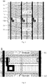
Fig. 3 and Fig. 4. Fig. 3 is a diagram of a pixel structure of a LCD according to an exemplary embodiment.Fig. 4 is a scale-up diagram of the area A shown inFig. 3 . Please note, this embodiment is more appropriate to be used in FFS/IPS LCD. TheLCD 30 comprises a plurality of gate lines G1 extending horizontally and a plurality of data lines D1 extending vertically. The gate lines G1 and the data lines D1 intersect each other to form a matrix to define a plurality ofpixel areas 31. Eachpixel area 31 comprises a pixel structure. The pixel structure comprises a pixel electrode P1, a gate line G1, a data line D1 and a transistor T1. The pixel electrode comprises at least two display domains. - The pixel electrode PI is located in the aperture of the pixel. The pixel electrode PI comprises two display domain, the 1st domain and the 2nd domain, to prevent the LCD from being blue or yellow when it is viewed at a large view angle. The two display domains are vertically arranged.
- The gate line G1 is located at the intersection of the two display domains (1st domain and 2nd domain) and the edge of the intersection overlaps the gate line G1. That is, the aperture of the pixel is divided by the gate line G1 and the edge of the intersection (the dividing line of the aperture) of the display domains overlaps the gate line G1. As shown in
Fig. 4 , thelower edge 41 of the 1st domain overlaps the gate line G1 and theupper edge 42 of the 2nd domain overlaps the gate line G1. In other words, the region where the liquid crystal molecules rotate in different direction overlaps the gate line. Since the gate line is made by non-transparent metal material, it covers the dark line caused by the liquid crystal molecules at the intersection and thus raises the aperture rate and transparent rate of the LCD. Furthermore, because the region where the liquid crystal molecules rotating differently are covered by the gate lines, there would be no display error when the LCD panel is pushed. This also raises the display quality. - The data line D1 is located at the edge of the aperture of the pixel structure (as shown in
Fig. 3 , the data line D1 is located at the left side of the aperture). In this embodiment, because one pixel electrode only comprises one data line and the data line is located at the sides of the pixel electrode (for example, in this embodiment, the data line is located at the left side) instead of being in the middle of the pixel electrode, this prevents from increasing the parasite capacitance, raising the temperature of the driver IC, and decreasing the reliability due to the data line. - The pixel electrode P1 is controlled by the data line D1 and gate line G1 via the transistor T1. One pixel comprises only one TFT. The TFT merely occupies a small area and thus raises the aperture rate of the LCD panel.
- In this embodiment, the pixel electrode PI extends in different directions in the two display domains (1st domain and 2nd domain). When the LCD works, the liquid crystal molecules in the two display domains respectively rotates clockwise and counterclockwise. This characteristic is used to improve the large view angle performance of the EFS LCD panel such that the LCD panel does not become blue or yellow when the LCD panel is viewed from its side. In this embodiment, the voltage levels of the two display domains of the pixel electrode PI are the same.
- In this embodiment, the
area 33 between the two pixel areas is a blank area. However, in the actual implementation, thearea 33 can comprises a common line to raise the flexibility of the layout. - Please refer to
Fig. 5 and Fig. 6. Fig. 5 is a diagram of a pixel structure of a LCD according to an exemplary embodiment.Fig. 6 is a scale-up diagram of the area B shown inFig. 5 . Please note, this embodiment is more appropriate to be used in HVA LCD. TheLCD 50 comprises a plurality of gate lines G1 extending horizontally and a plurality of data lines D1 extending vertically. The gate lines G1 and the data lines D1 intersect each other to form a matrix to define a plurality ofpixel areas 51. Eachpixel area 51 comprises a pixel structure. The pixel structure comprises a pixel electrode P1, a gate line G1, a common line COM1, a data line D1 and a transistor T1. The pixel electrode comprises at least four display domains. - The pixel electrode P1 is located in the aperture of the pixel. The pixel electrode P1 comprises four display domain, the 1st domain, the 2nd domain, the 3rd domain, and the 4th domain, to prevent the LCD from being blue or yellow when it is viewed at a large view angle. The 1st and 2nd domains are horizontally arranged (for example, one is in left of the other) and the 3rd and 4th domains are horizontally arranged.
- The 1st and 2nd domains are located above the gate line G1 and the lower edge of the 1st and 2nd domains overlaps the gate line G1.
- The 3rd and 4th domains are located under the common line COM1 and the upper edge of the 3rd and 4th domains overlap the common line COM1.
- The aperture of the pixel is divided by the gate line G1 and the common line COM1 and the gate line G1 and the common line COM1 are located at the intersection of the 1st and 2nd domains and the 3rd and 4th domains. Furthermore, the edges of the intersection overlaps the gate line G1 and the common line COM1.
- As shown in
Fig. 6 , at the intersection, alower edge 61 of the first display domain and the second display domain overlap the gate line G1, and anupper edge 62 of the third display domain and the fourth display domain overlaps the common line COM1. In this way, the regions where the liquid crystal molecules differently rotate overlap the gate line or the common line. Furthermore, the gate line and the common line are made by non-transparent metal material. Therefore, the dark line is covered by the gate line and the common line and does not exist in the aperture. Thus the aperture rate and the transparent rate are raised. In addition, because the regions where the liquid crystal molecules rotating differently are covered by the gate lines, there would be no display error when the LCD panel is pushed. This also raises the display quality. - In an exemplary embodiment, the pixel structure may comprise a pixel electrode P1, a gate line G1, a data line D1 and a transistor T1. The pixel electrode P1 comprises at least four display domains. The 1st domain and the 2nd domain are located above the gate line G1 and the lower edge of the 1st domain and the 2nd domain overlaps the gate line G1. In addition, the 3rd domain and the 4th domain are located under the gate line G1 and the upper edge of the 3rd domain and the 4th domain overlaps the gate line G1. That is, the aperture of the pixel is divided by the gate line G1 and the gate line G1 is located at the intersection of the 1st domain and the 2nd domain and the 3rd domain and the 4th domain. The edges of the intersection overlap the gate line G1. In this way, the regions where the liquid crystal molecules differently rotate overlap the gate line. Therefore, the dark line is covered by the gate line and does not exist in the aperture. Thus the aperture rate and the transparent rate are raised. In addition, because the regions where the liquid crystal molecules rotating differently are covered by the gate line, there would be no display error when the LCD panel is pushed. This also raises the display quality.
- The data line D1 is located at the edge of the aperture of the pixel (as shown in
Fig. 5 , the data line D1 is located at the left side of the aperture of the pixel). In this embodiment, one pixel electrode comprises only one data line. The data line D1 is located at the sides (in this embodiment, the data line is at the left side) instead of being in the middle of the pixel electrode. This prevents from increasing the parasite capacitance, raising the temperature of the driver IC, and decreasing the reliability due to the data line. - The pixel electrode P1 is controlled by the data line D1 and gate line G1 via the transistor T1. One pixel comprises only one TFT. The TFT merely occupies a small area and thus raises the aperture rate of the LCD panel.
- In this embodiment, the pixel electrode P1 extends in different directions in the four display domains (1st-4th domains). The liquid crystal molecules of the 1st domain rotate 45 degrees from the data line D1. The liquid crystal molecules of the 2nd domain rotate 135 degrees from the data line D1. The liquid crystal molecules of the 3rd domain rotate 225 degrees from the data line D1. The liquid crystal molecules of the 4th domain rotate 135 degrees from the data line D1. This characteristic is used to improve the large view angle performance of the HVA LCD panel such that the LCD panel does not become blue or yellow when the LCD panel is viewed from its side. In this embodiment, the four display domains of the pixel electrode PI have the same voltage level.
- Furthermore, in this embodiment, the
area 53 between the two pixel areas is a blank area. However, in the actual implementation, thearea 53 can comprises a common line to raise the flexibility of the layout. - Those skilled in the art will readily observe that numerous modifications and alterations of the device may be made while retaining the teachings of the present disclosure. Accordingly, the above disclosure should be construed as limited only by the metes and bounds of the appended claims.
Claims (14)
- A liquid crystal pixel structure, comprising:a pixel electrode, located in a pixel aperture, the pixel electrode comprising at least two vertically-arranged display domains, the at least two display domains have a same voltage level, the pixel electrode extends in different directions in the at least two display domains;a gate line, located at an intersection of the at least two display domains, and an edge of the intersection of the at least two display domains overlaps the gate line;a data line, located at an edge of the pixel aperture; anda transistor, configured to control the pixel electrode according to signal from the gate line and the data line.
- A liquid crystal pixel structure, comprising:a pixel electrode, located in a pixel aperture, the pixel electrode comprising at least two vertically-arranged display domains;a gate line, located at an intersection of the at least two display domains, and an edge of the intersection of the at least two display domains overlaps the gate line;a data line, located at an edge of the pixel aperture; anda transistor, configured to control the pixel electrode according to signal from the gate line and the data line.
- The liquid crystal pixel structure of claim 2, wherein the pixel electrode extends in different directions in the at least two display domains.
- The liquid crystal pixel structure of claim 2, wherein the at least two display domains have a same voltage level.
- A liquid crystal display (LCD), comprising:a plurality of gate lines extending in a horizontal direction; anda plurality of data lines extending in a vertical direction;wherein the plurality of gate lines and the plurality of data lines define a plurality of pixel areas and each of the pixel areas comprises the liquid crystal pixel structure as claimed in any one of claims 2-4.
- The LCD of claim 5, wherein an area between two adjacent pixel areas is a blank area or comprises a common line.
- A liquid crystal pixel structure, comprising:a pixel electrode, located in a pixel aperture, the pixel electrode comprising at least four display domains, wherein a first display domain and a second display domain of the at least four display domains are horizontally arranged, a third display domain and a fourth display domain of the at least four display domains are horizontally arranged, and the at least four display domains have a same voltage level;a gate line, wherein the first display domain and the second display domain are arranged above the gate line, a lower edge of the first display domain and the second display domain overlap the gate line, the third display domain and the fourth display domain are arranged under the gate line, and an upper edge of the third display domain and the fourth display domain overlaps the gate line;a data line, located at an edge of the pixel aperture; anda transistor, wherein the pixel electrode is controlled by the gate line and the data line via the transistor;wherein liquid crystal molecules of the first display domain, the second display domain, the third display domain, the fourth display domain respectively rotate 45 degrees, 135 degrees, 225 degrees, and 315 degrees from the data line.
- The liquid crystal pixel structure of claim 7, further comprising a common line,
wherein the first display domain and the second display domain are arranged above the gate line, the lower edges of the first display domain and the second display domain overlaps the gate line, the third display domain and the fourth display domain are arranged under the common line, and upper edges of the third display domain and the fourth display domain overlap the common line. - A liquid crystal pixel structure, comprising:a pixel electrode, located in a pixel aperture, the pixel electrode comprising at least four display domains, wherein a first display domain and a second display domain of the at least four display domains are horizontally arranged, a third display domain and a fourth display domain of the at least four display domains are horizontally arranged;a gate line, wherein the first display domain and the second display domain are arranged above the gate line, a lower edge of the first display domain and the second display domain overlap the gate line, the third display domain and the fourth display domain are arranged under the gate line, and an upper edge of the third display domain and the fourth display domain overlaps the gate line;a data line, located at an edge of the pixel aperture; anda transistor, wherein the pixel electrode is controlled by the gate line and the data line via the transistor.
- The liquid crystal pixel structure of claim 9, wherein liquid crystal molecules of the first display domain, the second display domain, the third display domain, the fourth display domain respectively rotate 45 degrees, 135 degrees, 225 degrees, and 315 degrees from the data line.
- The liquid crystal pixel structure of claim 9, wherein the at least four display domains have a same voltage level.
- The liquid crystal pixel structure of claim 9, further comprising a common line, wherein the first display domain and the second display domain are arranged above the gate line, the lower edges of the first display domain and the second display domain overlaps the gate line; the third display domain and the fourth display domain are arranged under the common line, and upper edges of the third display domain and the fourth display domain overlap the common line.
- A liquid crystal display (LCD), comprising:a plurality of gate lines extending in a horizontal direction; anda plurality of data lines extending in a vertical direction;wherein the plurality of gate lines and the plurality of data lines define a plurality of pixel areas and each of the pixel areas comprises the liquid crystal pixel structure as claimed in any one of claims 9-12.
- The LCD of claim 13, wherein an area between two adjacent pixel areas is a blank area or comprises a common line.
Applications Claiming Priority (2)
| Application Number | Priority Date | Filing Date | Title |
|---|---|---|---|
| CN201610458469.9A CN105938282A (en) | 2016-06-22 | 2016-06-22 | Liquid crystal display pixel structure and liquid crystal display device |
| PCT/CN2016/089715 WO2017219398A1 (en) | 2016-06-22 | 2016-07-12 | Liquid crystal display pixel structure and liquid crystal display device |
Publications (3)
| Publication Number | Publication Date |
|---|---|
| EP3477371A1 true EP3477371A1 (en) | 2019-05-01 |
| EP3477371A4 EP3477371A4 (en) | 2019-12-11 |
| EP3477371B1 EP3477371B1 (en) | 2021-09-01 |
Family
ID=56872510
Family Applications (1)
| Application Number | Title | Priority Date | Filing Date |
|---|---|---|---|
| EP16905938.3A Active EP3477371B1 (en) | 2016-06-22 | 2016-07-12 | Liquid crystal display pixel structure and liquid crystal display device |
Country Status (6)
| Country | Link |
|---|---|
| US (1) | US10185193B2 (en) |
| EP (1) | EP3477371B1 (en) |
| JP (1) | JP2019517683A (en) |
| KR (1) | KR102186131B1 (en) |
| CN (1) | CN105938282A (en) |
| WO (1) | WO2017219398A1 (en) |
Families Citing this family (10)
| Publication number | Priority date | Publication date | Assignee | Title |
|---|---|---|---|---|
| CN106502002A (en) * | 2016-12-13 | 2017-03-15 | 深圳市华星光电技术有限公司 | A kind of smooth alignment method, display panels and preparation method thereof |
| CN107153309B (en) * | 2017-07-18 | 2020-06-05 | 深圳市华星光电技术有限公司 | Array substrate, liquid crystal panel and display device |
| CN108490705B (en) * | 2018-04-13 | 2021-08-27 | 上海中航光电子有限公司 | Array substrate, liquid crystal display panel and display device |
| CN108732805B (en) * | 2018-05-28 | 2021-09-14 | 京东方科技集团股份有限公司 | Display substrate, display panel and display device |
| JP6888039B2 (en) * | 2019-02-27 | 2021-06-16 | パナソニック液晶ディスプレイ株式会社 | Liquid crystal display panel |
| US11333935B2 (en) | 2019-02-27 | 2022-05-17 | Panasonic Liquid Crystal Display Co., Ltd. | Liquid crystal display panel |
| CN111427199A (en) * | 2020-04-09 | 2020-07-17 | 深圳市华星光电半导体显示技术有限公司 | Pixel device and display panel |
| CN116324606B (en) * | 2021-04-27 | 2024-07-23 | 京东方科技集团股份有限公司 | Display substrate, liquid crystal display panel and display device |
| JP2024104787A (en) * | 2023-01-25 | 2024-08-06 | 株式会社ジャパンディスプレイ | Liquid crystal display device |
| WO2025218153A1 (en) * | 2024-04-19 | 2025-10-23 | Boe Technology Group Co., Ltd. | Array substrate and display apparatus |
Family Cites Families (22)
| Publication number | Priority date | Publication date | Assignee | Title |
|---|---|---|---|---|
| KR100471397B1 (en) * | 2001-05-31 | 2005-02-21 | 비오이 하이디스 테크놀로지 주식회사 | Apparatus for fringe field switching liquid crystal display and method for manufacturing the same |
| TWI243936B (en) * | 2003-12-11 | 2005-11-21 | Hannstar Display Corp | Structure of a display panel with compensating electrode |
| KR20060046241A (en) * | 2004-06-29 | 2006-05-17 | 엘지.필립스 엘시디 주식회사 | LCD |
| KR20080014317A (en) * | 2006-08-10 | 2008-02-14 | 삼성전자주식회사 | Display device and manufacturing method thereof |
| JP5073744B2 (en) * | 2007-06-27 | 2012-11-14 | シャープ株式会社 | Liquid crystal display |
| CN101398587B (en) * | 2007-09-29 | 2011-02-16 | 北京京东方光电科技有限公司 | Pixel structure of horizontal electric field type LCD device |
| JP2009103797A (en) * | 2007-10-22 | 2009-05-14 | Hitachi Displays Ltd | Liquid crystal display device |
| WO2011096390A1 (en) * | 2010-02-04 | 2011-08-11 | シャープ株式会社 | Liquid-crystal display device |
| TWI409560B (en) * | 2010-08-31 | 2013-09-21 | Chunghwa Picture Tubes Ltd | Pixel structure and pixel array |
| CN101976007B (en) * | 2010-09-14 | 2012-05-23 | 福建华映显示科技有限公司 | Pixel structure and pixel array |
| JP5551553B2 (en) * | 2010-09-29 | 2014-07-16 | 株式会社ジャパンディスプレイ | Liquid crystal display |
| KR101820032B1 (en) * | 2010-09-30 | 2018-01-19 | 삼성디스플레이 주식회사 | Thin film transistor panel, liquid crystal display device, and method to repair thereof |
| KR20130018057A (en) * | 2011-08-12 | 2013-02-20 | 엘지디스플레이 주식회사 | Array substrate for in-plane switching mode liquid crystal display device |
| KR20130059181A (en) * | 2011-11-28 | 2013-06-05 | 엘지디스플레이 주식회사 | Liquid crystal display device for in-plane switching mode and method for fabricating the same |
| CN202339463U (en) * | 2011-11-29 | 2012-07-18 | 北京京东方光电科技有限公司 | Pixel structure of thin film transistor liquid crystal display and liquid crystal display |
| KR101929345B1 (en) | 2011-12-21 | 2018-12-17 | 엘지디스플레이 주식회사 | Fringe field switching liquid crystal display device |
| US8988332B2 (en) * | 2012-07-18 | 2015-03-24 | Shenzhen China Star Optoelectronics Technology Co., Ltd. | Pixel structure and corresponding liquid crystal display device |
| KR102249284B1 (en) * | 2014-12-12 | 2021-05-07 | 삼성디스플레이 주식회사 | Liquid crystal display |
| CN104536222A (en) * | 2014-12-22 | 2015-04-22 | 深圳市华星光电技术有限公司 | FFS array substrate and liquid crystal display panel |
| CN104914634B (en) * | 2015-06-17 | 2019-04-05 | 南京中电熊猫平板显示科技有限公司 | Liquid crystal display panel and its pixels |
| CN104932162B (en) | 2015-06-30 | 2019-02-12 | 厦门天马微电子有限公司 | Array substrate and liquid crystal display panel |
| KR102423398B1 (en) * | 2015-10-30 | 2022-07-20 | 엘지디스플레이 주식회사 | Autostereoscopic 3d display device |
-
2016
- 2016-06-22 CN CN201610458469.9A patent/CN105938282A/en active Pending
- 2016-07-12 KR KR1020197001906A patent/KR102186131B1/en active Active
- 2016-07-12 EP EP16905938.3A patent/EP3477371B1/en active Active
- 2016-07-12 JP JP2018563584A patent/JP2019517683A/en active Pending
- 2016-07-12 US US15/313,131 patent/US10185193B2/en active Active
- 2016-07-12 WO PCT/CN2016/089715 patent/WO2017219398A1/en not_active Ceased
Also Published As
| Publication number | Publication date |
|---|---|
| EP3477371A4 (en) | 2019-12-11 |
| CN105938282A (en) | 2016-09-14 |
| KR102186131B1 (en) | 2020-12-03 |
| US10185193B2 (en) | 2019-01-22 |
| EP3477371B1 (en) | 2021-09-01 |
| WO2017219398A1 (en) | 2017-12-28 |
| KR20190016590A (en) | 2019-02-18 |
| US20170371212A1 (en) | 2017-12-28 |
| JP2019517683A (en) | 2019-06-24 |
Similar Documents
| Publication | Publication Date | Title |
|---|---|---|
| EP3477371B1 (en) | Liquid crystal display pixel structure and liquid crystal display device | |
| EP3872561B1 (en) | Array substrate | |
| US20140104547A1 (en) | Pixel structure of transparent liquid crystal display panel | |
| US10401685B2 (en) | Array substrate, manufacturing method thereof and display device | |
| JP6745732B2 (en) | Liquid crystal display panel and liquid crystal display device | |
| US9377653B2 (en) | PVA pixel electrode and liquid crystal display apparatus using the same | |
| KR102653472B1 (en) | Display device | |
| KR102127761B1 (en) | Thin film transistor substrate and liquid crystal display | |
| US10627680B2 (en) | Display panel and display device | |
| CN113485051A (en) | Array substrate and display panel | |
| KR20160117786A (en) | Liquid crystal display device | |
| KR101582947B1 (en) | Liquid crystal display | |
| KR20210073807A (en) | Liquid crystal display panel | |
| JP4516432B2 (en) | Liquid crystal display | |
| US9372374B2 (en) | Liquid crystal display device with unit pixel having rhombus-like plate portion | |
| US9846342B2 (en) | Liquid crystal display device | |
| US20220317492A1 (en) | Liquid crystal display panel and liquid crystal display device | |
| JP5131525B2 (en) | Active matrix liquid crystal display device | |
| KR101794283B1 (en) | Thin film transtistor array panel and liquid crystal display | |
| US20150378221A1 (en) | Liquid crystal display | |
| KR20160129158A (en) | Liquid crystal display | |
| KR20110033706A (en) | LCD Display | |
| KR102401608B1 (en) | liquid crystal display | |
| KR20160067301A (en) | Thin film transistor substrate and liquid crystal display | |
| US9195101B2 (en) | Liquid crystal display panel comprising a pixel electrode that includes one uniformly planar electrode region and one or more finely patterned electrode regions |
Legal Events
| Date | Code | Title | Description |
|---|---|---|---|
| STAA | Information on the status of an ep patent application or granted ep patent |
Free format text: STATUS: THE INTERNATIONAL PUBLICATION HAS BEEN MADE |
|
| PUAI | Public reference made under article 153(3) epc to a published international application that has entered the european phase |
Free format text: ORIGINAL CODE: 0009012 |
|
| STAA | Information on the status of an ep patent application or granted ep patent |
Free format text: STATUS: REQUEST FOR EXAMINATION WAS MADE |
|
| 17P | Request for examination filed |
Effective date: 20190115 |
|
| AK | Designated contracting states |
Kind code of ref document: A1 Designated state(s): AL AT BE BG CH CY CZ DE DK EE ES FI FR GB GR HR HU IE IS IT LI LT LU LV MC MK MT NL NO PL PT RO RS SE SI SK SM TR |
|
| AX | Request for extension of the european patent |
Extension state: BA ME |
|
| DAV | Request for validation of the european patent (deleted) | ||
| DAX | Request for extension of the european patent (deleted) | ||
| A4 | Supplementary search report drawn up and despatched |
Effective date: 20191112 |
|
| RIC1 | Information provided on ipc code assigned before grant |
Ipc: G02F 1/1368 20060101ALI20191106BHEP Ipc: G02F 1/1362 20060101AFI20191106BHEP Ipc: G02F 1/1343 20060101ALI20191106BHEP |
|
| GRAP | Despatch of communication of intention to grant a patent |
Free format text: ORIGINAL CODE: EPIDOSNIGR1 |
|
| STAA | Information on the status of an ep patent application or granted ep patent |
Free format text: STATUS: GRANT OF PATENT IS INTENDED |
|
| INTG | Intention to grant announced |
Effective date: 20210326 |
|
| GRAS | Grant fee paid |
Free format text: ORIGINAL CODE: EPIDOSNIGR3 |
|
| GRAA | (expected) grant |
Free format text: ORIGINAL CODE: 0009210 |
|
| STAA | Information on the status of an ep patent application or granted ep patent |
Free format text: STATUS: THE PATENT HAS BEEN GRANTED |
|
| AK | Designated contracting states |
Kind code of ref document: B1 Designated state(s): AL AT BE BG CH CY CZ DE DK EE ES FI FR GB GR HR HU IE IS IT LI LT LU LV MC MK MT NL NO PL PT RO RS SE SI SK SM TR |
|
| REG | Reference to a national code |
Ref country code: GB Ref legal event code: FG4D |
|
| REG | Reference to a national code |
Ref country code: CH Ref legal event code: EP Ref country code: AT Ref legal event code: REF Ref document number: 1426847 Country of ref document: AT Kind code of ref document: T Effective date: 20210915 |
|
| REG | Reference to a national code |
Ref country code: DE Ref legal event code: R096 Ref document number: 602016063307 Country of ref document: DE |
|
| REG | Reference to a national code |
Ref country code: IE Ref legal event code: FG4D |
|
| REG | Reference to a national code |
Ref country code: LT Ref legal event code: MG9D |
|
| REG | Reference to a national code |
Ref country code: NL Ref legal event code: MP Effective date: 20210901 |
|
| PG25 | Lapsed in a contracting state [announced via postgrant information from national office to epo] |
Ref country code: RS Free format text: LAPSE BECAUSE OF FAILURE TO SUBMIT A TRANSLATION OF THE DESCRIPTION OR TO PAY THE FEE WITHIN THE PRESCRIBED TIME-LIMIT Effective date: 20210901 Ref country code: SE Free format text: LAPSE BECAUSE OF FAILURE TO SUBMIT A TRANSLATION OF THE DESCRIPTION OR TO PAY THE FEE WITHIN THE PRESCRIBED TIME-LIMIT Effective date: 20210901 Ref country code: NO Free format text: LAPSE BECAUSE OF FAILURE TO SUBMIT A TRANSLATION OF THE DESCRIPTION OR TO PAY THE FEE WITHIN THE PRESCRIBED TIME-LIMIT Effective date: 20211201 Ref country code: FI Free format text: LAPSE BECAUSE OF FAILURE TO SUBMIT A TRANSLATION OF THE DESCRIPTION OR TO PAY THE FEE WITHIN THE PRESCRIBED TIME-LIMIT Effective date: 20210901 Ref country code: ES Free format text: LAPSE BECAUSE OF FAILURE TO SUBMIT A TRANSLATION OF THE DESCRIPTION OR TO PAY THE FEE WITHIN THE PRESCRIBED TIME-LIMIT Effective date: 20210901 Ref country code: HR Free format text: LAPSE BECAUSE OF FAILURE TO SUBMIT A TRANSLATION OF THE DESCRIPTION OR TO PAY THE FEE WITHIN THE PRESCRIBED TIME-LIMIT Effective date: 20210901 Ref country code: BG Free format text: LAPSE BECAUSE OF FAILURE TO SUBMIT A TRANSLATION OF THE DESCRIPTION OR TO PAY THE FEE WITHIN THE PRESCRIBED TIME-LIMIT Effective date: 20211201 Ref country code: LT Free format text: LAPSE BECAUSE OF FAILURE TO SUBMIT A TRANSLATION OF THE DESCRIPTION OR TO PAY THE FEE WITHIN THE PRESCRIBED TIME-LIMIT Effective date: 20210901 |
|
| REG | Reference to a national code |
Ref country code: AT Ref legal event code: MK05 Ref document number: 1426847 Country of ref document: AT Kind code of ref document: T Effective date: 20210901 |
|
| PG25 | Lapsed in a contracting state [announced via postgrant information from national office to epo] |
Ref country code: PL Free format text: LAPSE BECAUSE OF FAILURE TO SUBMIT A TRANSLATION OF THE DESCRIPTION OR TO PAY THE FEE WITHIN THE PRESCRIBED TIME-LIMIT Effective date: 20210901 Ref country code: LV Free format text: LAPSE BECAUSE OF FAILURE TO SUBMIT A TRANSLATION OF THE DESCRIPTION OR TO PAY THE FEE WITHIN THE PRESCRIBED TIME-LIMIT Effective date: 20210901 Ref country code: GR Free format text: LAPSE BECAUSE OF FAILURE TO SUBMIT A TRANSLATION OF THE DESCRIPTION OR TO PAY THE FEE WITHIN THE PRESCRIBED TIME-LIMIT Effective date: 20211202 |
|
| PG25 | Lapsed in a contracting state [announced via postgrant information from national office to epo] |
Ref country code: AT Free format text: LAPSE BECAUSE OF FAILURE TO SUBMIT A TRANSLATION OF THE DESCRIPTION OR TO PAY THE FEE WITHIN THE PRESCRIBED TIME-LIMIT Effective date: 20210901 |
|
| PG25 | Lapsed in a contracting state [announced via postgrant information from national office to epo] |
Ref country code: IS Free format text: LAPSE BECAUSE OF FAILURE TO SUBMIT A TRANSLATION OF THE DESCRIPTION OR TO PAY THE FEE WITHIN THE PRESCRIBED TIME-LIMIT Effective date: 20220101 Ref country code: SM Free format text: LAPSE BECAUSE OF FAILURE TO SUBMIT A TRANSLATION OF THE DESCRIPTION OR TO PAY THE FEE WITHIN THE PRESCRIBED TIME-LIMIT Effective date: 20210901 Ref country code: SK Free format text: LAPSE BECAUSE OF FAILURE TO SUBMIT A TRANSLATION OF THE DESCRIPTION OR TO PAY THE FEE WITHIN THE PRESCRIBED TIME-LIMIT Effective date: 20210901 Ref country code: RO Free format text: LAPSE BECAUSE OF FAILURE TO SUBMIT A TRANSLATION OF THE DESCRIPTION OR TO PAY THE FEE WITHIN THE PRESCRIBED TIME-LIMIT Effective date: 20210901 Ref country code: PT Free format text: LAPSE BECAUSE OF FAILURE TO SUBMIT A TRANSLATION OF THE DESCRIPTION OR TO PAY THE FEE WITHIN THE PRESCRIBED TIME-LIMIT Effective date: 20220103 Ref country code: NL Free format text: LAPSE BECAUSE OF FAILURE TO SUBMIT A TRANSLATION OF THE DESCRIPTION OR TO PAY THE FEE WITHIN THE PRESCRIBED TIME-LIMIT Effective date: 20210901 Ref country code: EE Free format text: LAPSE BECAUSE OF FAILURE TO SUBMIT A TRANSLATION OF THE DESCRIPTION OR TO PAY THE FEE WITHIN THE PRESCRIBED TIME-LIMIT Effective date: 20210901 Ref country code: CZ Free format text: LAPSE BECAUSE OF FAILURE TO SUBMIT A TRANSLATION OF THE DESCRIPTION OR TO PAY THE FEE WITHIN THE PRESCRIBED TIME-LIMIT Effective date: 20210901 Ref country code: AL Free format text: LAPSE BECAUSE OF FAILURE TO SUBMIT A TRANSLATION OF THE DESCRIPTION OR TO PAY THE FEE WITHIN THE PRESCRIBED TIME-LIMIT Effective date: 20210901 |
|
| REG | Reference to a national code |
Ref country code: DE Ref legal event code: R097 Ref document number: 602016063307 Country of ref document: DE |
|
| PLBE | No opposition filed within time limit |
Free format text: ORIGINAL CODE: 0009261 |
|
| STAA | Information on the status of an ep patent application or granted ep patent |
Free format text: STATUS: NO OPPOSITION FILED WITHIN TIME LIMIT |
|
| PG25 | Lapsed in a contracting state [announced via postgrant information from national office to epo] |
Ref country code: IT Free format text: LAPSE BECAUSE OF FAILURE TO SUBMIT A TRANSLATION OF THE DESCRIPTION OR TO PAY THE FEE WITHIN THE PRESCRIBED TIME-LIMIT Effective date: 20210901 Ref country code: DK Free format text: LAPSE BECAUSE OF FAILURE TO SUBMIT A TRANSLATION OF THE DESCRIPTION OR TO PAY THE FEE WITHIN THE PRESCRIBED TIME-LIMIT Effective date: 20210901 |
|
| 26N | No opposition filed |
Effective date: 20220602 |
|
| PG25 | Lapsed in a contracting state [announced via postgrant information from national office to epo] |
Ref country code: SI Free format text: LAPSE BECAUSE OF FAILURE TO SUBMIT A TRANSLATION OF THE DESCRIPTION OR TO PAY THE FEE WITHIN THE PRESCRIBED TIME-LIMIT Effective date: 20210901 |
|
| REG | Reference to a national code |
Ref country code: DE Ref legal event code: R082 Ref document number: 602016063307 Country of ref document: DE Representative=s name: PATENTANWAELTE OLBRICHT, BUCHHOLD, KEULERTZ PA, DE |
|
| PG25 | Lapsed in a contracting state [announced via postgrant information from national office to epo] |
Ref country code: MC Free format text: LAPSE BECAUSE OF FAILURE TO SUBMIT A TRANSLATION OF THE DESCRIPTION OR TO PAY THE FEE WITHIN THE PRESCRIBED TIME-LIMIT Effective date: 20210901 |
|
| REG | Reference to a national code |
Ref country code: CH Ref legal event code: PL |
|
| GBPC | Gb: european patent ceased through non-payment of renewal fee |
Effective date: 20220712 |
|
| REG | Reference to a national code |
Ref country code: BE Ref legal event code: MM Effective date: 20220731 |
|
| PG25 | Lapsed in a contracting state [announced via postgrant information from national office to epo] |
Ref country code: LU Free format text: LAPSE BECAUSE OF NON-PAYMENT OF DUE FEES Effective date: 20220712 Ref country code: LI Free format text: LAPSE BECAUSE OF NON-PAYMENT OF DUE FEES Effective date: 20220731 Ref country code: FR Free format text: LAPSE BECAUSE OF NON-PAYMENT OF DUE FEES Effective date: 20220731 Ref country code: CH Free format text: LAPSE BECAUSE OF NON-PAYMENT OF DUE FEES Effective date: 20220731 |
|
| PG25 | Lapsed in a contracting state [announced via postgrant information from national office to epo] |
Ref country code: GB Free format text: LAPSE BECAUSE OF NON-PAYMENT OF DUE FEES Effective date: 20220712 Ref country code: BE Free format text: LAPSE BECAUSE OF NON-PAYMENT OF DUE FEES Effective date: 20220731 |
|
| P01 | Opt-out of the competence of the unified patent court (upc) registered |
Effective date: 20230530 |
|
| PG25 | Lapsed in a contracting state [announced via postgrant information from national office to epo] |
Ref country code: IE Free format text: LAPSE BECAUSE OF NON-PAYMENT OF DUE FEES Effective date: 20220712 |
|
| PG25 | Lapsed in a contracting state [announced via postgrant information from national office to epo] |
Ref country code: HU Free format text: LAPSE BECAUSE OF FAILURE TO SUBMIT A TRANSLATION OF THE DESCRIPTION OR TO PAY THE FEE WITHIN THE PRESCRIBED TIME-LIMIT; INVALID AB INITIO Effective date: 20160712 |
|
| PG25 | Lapsed in a contracting state [announced via postgrant information from national office to epo] |
Ref country code: MK Free format text: LAPSE BECAUSE OF FAILURE TO SUBMIT A TRANSLATION OF THE DESCRIPTION OR TO PAY THE FEE WITHIN THE PRESCRIBED TIME-LIMIT Effective date: 20210901 Ref country code: CY Free format text: LAPSE BECAUSE OF FAILURE TO SUBMIT A TRANSLATION OF THE DESCRIPTION OR TO PAY THE FEE WITHIN THE PRESCRIBED TIME-LIMIT Effective date: 20210901 |
|
| PG25 | Lapsed in a contracting state [announced via postgrant information from national office to epo] |
Ref country code: MT Free format text: LAPSE BECAUSE OF FAILURE TO SUBMIT A TRANSLATION OF THE DESCRIPTION OR TO PAY THE FEE WITHIN THE PRESCRIBED TIME-LIMIT Effective date: 20210901 |
|
| PGFP | Annual fee paid to national office [announced via postgrant information from national office to epo] |
Ref country code: DE Payment date: 20250722 Year of fee payment: 10 |
|
| PG25 | Lapsed in a contracting state [announced via postgrant information from national office to epo] |
Ref country code: TR Free format text: LAPSE BECAUSE OF FAILURE TO SUBMIT A TRANSLATION OF THE DESCRIPTION OR TO PAY THE FEE WITHIN THE PRESCRIBED TIME-LIMIT Effective date: 20210901 |