EP3471197B1 - Hochfrequenzsysteme mit integrierten anzeigen und verfahren zur formung davon - Google Patents
Hochfrequenzsysteme mit integrierten anzeigen und verfahren zur formung davon Download PDFInfo
- Publication number
- EP3471197B1 EP3471197B1 EP18197938.6A EP18197938A EP3471197B1 EP 3471197 B1 EP3471197 B1 EP 3471197B1 EP 18197938 A EP18197938 A EP 18197938A EP 3471197 B1 EP3471197 B1 EP 3471197B1
- Authority
- EP
- European Patent Office
- Prior art keywords
- substrate
- antenna
- antennas
- chip
- signals
- Prior art date
- Legal status (The legal status is an assumption and is not a legal conclusion. Google has not performed a legal analysis and makes no representation as to the accuracy of the status listed.)
- Active
Links
Images


Classifications
-
- G—PHYSICS
- G06—COMPUTING OR CALCULATING; COUNTING
- G06F—ELECTRIC DIGITAL DATA PROCESSING
- G06F1/00—Details not covered by groups G06F3/00 - G06F13/00 and G06F21/00
- G06F1/16—Constructional details or arrangements
- G06F1/1613—Constructional details or arrangements for portable computers
- G06F1/1633—Constructional details or arrangements of portable computers not specific to the type of enclosures covered by groups G06F1/1615 - G06F1/1626
- G06F1/1637—Details related to the display arrangement, including those related to the mounting of the display in the housing
-
- G—PHYSICS
- G01—MEASURING; TESTING
- G01S—RADIO DIRECTION-FINDING; RADIO NAVIGATION; DETERMINING DISTANCE OR VELOCITY BY USE OF RADIO WAVES; LOCATING OR PRESENCE-DETECTING BY USE OF THE REFLECTION OR RERADIATION OF RADIO WAVES; ANALOGOUS ARRANGEMENTS USING OTHER WAVES
- G01S13/00—Systems using the reflection or reradiation of radio waves, e.g. radar systems; Analogous systems using reflection or reradiation of waves whose nature or wavelength is irrelevant or unspecified
- G01S13/02—Systems using reflection of radio waves, e.g. primary radar systems; Analogous systems
- G01S13/06—Systems determining position data of a target
- G01S13/08—Systems for measuring distance only
- G01S13/32—Systems for measuring distance only using transmission of continuous waves, whether amplitude-, frequency-, or phase-modulated, or unmodulated
- G01S13/34—Systems for measuring distance only using transmission of continuous waves, whether amplitude-, frequency-, or phase-modulated, or unmodulated using transmission of continuous, frequency-modulated waves while heterodyning the received signal, or a signal derived therefrom, with a locally-generated signal related to the contemporaneously transmitted signal
-
- G—PHYSICS
- G01—MEASURING; TESTING
- G01S—RADIO DIRECTION-FINDING; RADIO NAVIGATION; DETERMINING DISTANCE OR VELOCITY BY USE OF RADIO WAVES; LOCATING OR PRESENCE-DETECTING BY USE OF THE REFLECTION OR RERADIATION OF RADIO WAVES; ANALOGOUS ARRANGEMENTS USING OTHER WAVES
- G01S13/00—Systems using the reflection or reradiation of radio waves, e.g. radar systems; Analogous systems using reflection or reradiation of waves whose nature or wavelength is irrelevant or unspecified
- G01S13/02—Systems using reflection of radio waves, e.g. primary radar systems; Analogous systems
- G01S13/06—Systems determining position data of a target
- G01S13/42—Simultaneous measurement of distance and other co-ordinates
- G01S13/44—Monopulse radar, i.e. simultaneous lobing
-
- G—PHYSICS
- G01—MEASURING; TESTING
- G01S—RADIO DIRECTION-FINDING; RADIO NAVIGATION; DETERMINING DISTANCE OR VELOCITY BY USE OF RADIO WAVES; LOCATING OR PRESENCE-DETECTING BY USE OF THE REFLECTION OR RERADIATION OF RADIO WAVES; ANALOGOUS ARRANGEMENTS USING OTHER WAVES
- G01S13/00—Systems using the reflection or reradiation of radio waves, e.g. radar systems; Analogous systems using reflection or reradiation of waves whose nature or wavelength is irrelevant or unspecified
- G01S13/88—Radar or analogous systems specially adapted for specific applications
-
- G—PHYSICS
- G01—MEASURING; TESTING
- G01S—RADIO DIRECTION-FINDING; RADIO NAVIGATION; DETERMINING DISTANCE OR VELOCITY BY USE OF RADIO WAVES; LOCATING OR PRESENCE-DETECTING BY USE OF THE REFLECTION OR RERADIATION OF RADIO WAVES; ANALOGOUS ARRANGEMENTS USING OTHER WAVES
- G01S7/00—Details of systems according to groups G01S13/00, G01S15/00, G01S17/00
- G01S7/02—Details of systems according to groups G01S13/00, G01S15/00, G01S17/00 of systems according to group G01S13/00
- G01S7/027—Constructional details of housings, e.g. form, type, material or ruggedness
-
- G—PHYSICS
- G01—MEASURING; TESTING
- G01S—RADIO DIRECTION-FINDING; RADIO NAVIGATION; DETERMINING DISTANCE OR VELOCITY BY USE OF RADIO WAVES; LOCATING OR PRESENCE-DETECTING BY USE OF THE REFLECTION OR RERADIATION OF RADIO WAVES; ANALOGOUS ARRANGEMENTS USING OTHER WAVES
- G01S7/00—Details of systems according to groups G01S13/00, G01S15/00, G01S17/00
- G01S7/02—Details of systems according to groups G01S13/00, G01S15/00, G01S17/00 of systems according to group G01S13/00
- G01S7/04—Display arrangements
-
- G—PHYSICS
- G06—COMPUTING OR CALCULATING; COUNTING
- G06F—ELECTRIC DIGITAL DATA PROCESSING
- G06F1/00—Details not covered by groups G06F3/00 - G06F13/00 and G06F21/00
- G06F1/16—Constructional details or arrangements
- G06F1/1613—Constructional details or arrangements for portable computers
- G06F1/1633—Constructional details or arrangements of portable computers not specific to the type of enclosures covered by groups G06F1/1615 - G06F1/1626
- G06F1/1684—Constructional details or arrangements related to integrated I/O peripherals not covered by groups G06F1/1635 - G06F1/1675
- G06F1/1698—Constructional details or arrangements related to integrated I/O peripherals not covered by groups G06F1/1635 - G06F1/1675 the I/O peripheral being a sending/receiving arrangement to establish a cordless communication link, e.g. radio or infrared link, integrated cellular phone
-
- G—PHYSICS
- G06—COMPUTING OR CALCULATING; COUNTING
- G06F—ELECTRIC DIGITAL DATA PROCESSING
- G06F3/00—Input arrangements for transferring data to be processed into a form capable of being handled by the computer; Output arrangements for transferring data from processing unit to output unit, e.g. interface arrangements
- G06F3/01—Input arrangements or combined input and output arrangements for interaction between user and computer
- G06F3/017—Gesture based interaction, e.g. based on a set of recognized hand gestures
-
- H—ELECTRICITY
- H01—ELECTRIC ELEMENTS
- H01Q—ANTENNAS, i.e. RADIO AERIALS
- H01Q1/00—Details of, or arrangements associated with, antennas
- H01Q1/12—Supports; Mounting means
- H01Q1/22—Supports; Mounting means by structural association with other equipment or articles
- H01Q1/2258—Supports; Mounting means by structural association with other equipment or articles used with computer equipment
-
- H—ELECTRICITY
- H01—ELECTRIC ELEMENTS
- H01Q—ANTENNAS, i.e. RADIO AERIALS
- H01Q1/00—Details of, or arrangements associated with, antennas
- H01Q1/12—Supports; Mounting means
- H01Q1/22—Supports; Mounting means by structural association with other equipment or articles
- H01Q1/2283—Supports; Mounting means by structural association with other equipment or articles mounted in or on the surface of a semiconductor substrate as a chip-type antenna or integrated with other components into an IC package
-
- H—ELECTRICITY
- H01—ELECTRIC ELEMENTS
- H01Q—ANTENNAS, i.e. RADIO AERIALS
- H01Q1/00—Details of, or arrangements associated with, antennas
- H01Q1/12—Supports; Mounting means
- H01Q1/22—Supports; Mounting means by structural association with other equipment or articles
- H01Q1/24—Supports; Mounting means by structural association with other equipment or articles with receiving set
- H01Q1/241—Supports; Mounting means by structural association with other equipment or articles with receiving set used in mobile communications, e.g. GSM
- H01Q1/242—Supports; Mounting means by structural association with other equipment or articles with receiving set used in mobile communications, e.g. GSM specially adapted for hand-held use
- H01Q1/243—Supports; Mounting means by structural association with other equipment or articles with receiving set used in mobile communications, e.g. GSM specially adapted for hand-held use with built-in antennas
-
- H—ELECTRICITY
- H01—ELECTRIC ELEMENTS
- H01Q—ANTENNAS, i.e. RADIO AERIALS
- H01Q1/00—Details of, or arrangements associated with, antennas
- H01Q1/27—Adaptation for use in or on movable bodies
- H01Q1/273—Adaptation for carrying or wearing by persons or animals
-
- H—ELECTRICITY
- H01—ELECTRIC ELEMENTS
- H01Q—ANTENNAS, i.e. RADIO AERIALS
- H01Q1/00—Details of, or arrangements associated with, antennas
- H01Q1/36—Structural form of radiating elements, e.g. cone, spiral, umbrella; Particular materials used therewith
- H01Q1/38—Structural form of radiating elements, e.g. cone, spiral, umbrella; Particular materials used therewith formed by a conductive layer on an insulating support
-
- H—ELECTRICITY
- H01—ELECTRIC ELEMENTS
- H01Q—ANTENNAS, i.e. RADIO AERIALS
- H01Q1/00—Details of, or arrangements associated with, antennas
- H01Q1/40—Radiating elements coated with or embedded in protective material
-
- H—ELECTRICITY
- H01—ELECTRIC ELEMENTS
- H01Q—ANTENNAS, i.e. RADIO AERIALS
- H01Q9/00—Electrically-short antennas having dimensions not more than twice the operating wavelength and consisting of conductive active radiating elements
- H01Q9/04—Resonant antennas
- H01Q9/0407—Substantially flat resonant element parallel to ground plane, e.g. patch antenna
- H01Q9/045—Substantially flat resonant element parallel to ground plane, e.g. patch antenna with particular feeding means
- H01Q9/0457—Substantially flat resonant element parallel to ground plane, e.g. patch antenna with particular feeding means electromagnetically coupled to the feed line
-
- H—ELECTRICITY
- H04—ELECTRIC COMMUNICATION TECHNIQUE
- H04B—TRANSMISSION
- H04B1/00—Details of transmission systems, not covered by a single one of groups H04B3/00 - H04B13/00; Details of transmission systems not characterised by the medium used for transmission
- H04B1/38—Transceivers, i.e. devices in which transmitter and receiver form a structural unit and in which at least one part is used for functions of transmitting and receiving
- H04B1/40—Circuits
-
- H—ELECTRICITY
- H04—ELECTRIC COMMUNICATION TECHNIQUE
- H04M—TELEPHONIC COMMUNICATION
- H04M1/00—Substation equipment, e.g. for use by subscribers
- H04M1/02—Constructional features of telephone sets
- H04M1/0202—Portable telephone sets, e.g. cordless phones, mobile phones or bar type handsets
- H04M1/026—Details of the structure or mounting of specific components
- H04M1/0266—Details of the structure or mounting of specific components for a display module assembly
-
- G—PHYSICS
- G01—MEASURING; TESTING
- G01S—RADIO DIRECTION-FINDING; RADIO NAVIGATION; DETERMINING DISTANCE OR VELOCITY BY USE OF RADIO WAVES; LOCATING OR PRESENCE-DETECTING BY USE OF THE REFLECTION OR RERADIATION OF RADIO WAVES; ANALOGOUS ARRANGEMENTS USING OTHER WAVES
- G01S13/00—Systems using the reflection or reradiation of radio waves, e.g. radar systems; Analogous systems using reflection or reradiation of waves whose nature or wavelength is irrelevant or unspecified
- G01S13/02—Systems using reflection of radio waves, e.g. primary radar systems; Analogous systems
- G01S2013/0236—Special technical features
- G01S2013/0245—Radar with phased array antenna
-
- G—PHYSICS
- G01—MEASURING; TESTING
- G01S—RADIO DIRECTION-FINDING; RADIO NAVIGATION; DETERMINING DISTANCE OR VELOCITY BY USE OF RADIO WAVES; LOCATING OR PRESENCE-DETECTING BY USE OF THE REFLECTION OR RERADIATION OF RADIO WAVES; ANALOGOUS ARRANGEMENTS USING OTHER WAVES
- G01S7/00—Details of systems according to groups G01S13/00, G01S15/00, G01S17/00
- G01S7/02—Details of systems according to groups G01S13/00, G01S15/00, G01S17/00 of systems according to group G01S13/00
- G01S7/35—Details of non-pulse systems
- G01S7/352—Receivers
- G01S7/356—Receivers involving particularities of FFT processing
-
- H—ELECTRICITY
- H01—ELECTRIC ELEMENTS
- H01Q—ANTENNAS, i.e. RADIO AERIALS
- H01Q21/00—Antenna arrays or systems
- H01Q21/06—Arrays of individually energised antenna units similarly polarised and spaced apart
- H01Q21/061—Two dimensional planar arrays
- H01Q21/065—Patch antenna array
Definitions
- the present invention relates generally to a radio frequency system, and, in particular embodiments, to structures of radio frequency systems integrated with displays, methods of formation, and methods of operation thereof.
- Portable devices such as tablets, smart phones, and smart watches have become popular recently due to the rapid advancement in low-cost semiconductor technologies.
- Portable devices as well as other electronic devices may incorporate antenna elements for radio frequency (RF) communication as well as for radar applications such as object ranging, tracking, and identification.
- RF radio frequency
- multiple antenna elements may be utilized for beamforming, transmit diversity and multiple input, multiple output (MIMO) configurations, and also as radar sensors that can detect user motions (known as gesture sensors).
- MIMO multiple input, multiple output
- the wireless circuitry includes one or more antennas.
- the antennas include phased antenna arrays each of which includes multiple antenna elements. Phased antenna arrays are mounted along edges of a housing for the electronic device, behind a dielectric window such as a dielectric logo window in the housing, in alignment with dielectric housing portions at corners of the housing, or elsewhere in the electronic device.
- a phased antenna array includes arrays of patch antenna elements on dielectric layers separated by a ground layer.
- a baseband processor distributes wireless signals to the phased antenna arrays at intermediate frequencies over intermediate frequency signal paths.
- Transceiver circuits at the phased antenna arrays may include upconverters and downconverters coupled to the intermediate frequency signal paths.
- a radio frequency, RF, system as defined by independent claim 1 or by independent claim 2 is presented.
- Advantageous modifications of the RF systems are defined by the dependent claims.
- Portable devices may utilize antenna elements for beamforming, transmit diversity and MIMO configurations, and as radar sensors that can detect user motions (known as gesture sensors).
- Gesture sensors may be configured in a portable device as an interface to control functionality of the device as well as to gather information about objects in the area around the portable device.
- a radar-based gesture detection system is used to directly control a device such as a computer, a smartphone, or a tablet computer, or to control a remote device such as a vehicle, an electronic system within a building, or a home appliance.
- a device such as a computer, a smartphone, or a tablet computer
- a remote device such as a vehicle, an electronic system within a building, or a home appliance.
- the remote device is a car
- an embodiment gesture detection system allows a human actor to control various operations of the car from outside the car.
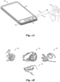
- FIG. 1A illustrates an example radio frequency (RF) system application in which a portable device 100 is controlled using various hand gestures.
- portable device 100 may be a smart phone and includes a display element 102 physically coupled to a sensor region 104.
- sensor region 104 transmits RF signals 110 to target 114, which may be a human hand, and receives reflected RF signals 112 that are reflected by target 114. These reflected RF signals 112 are processed by the radar system to determine the position and motion of target 114 and/or to determine whether target 114 is providing a particular gesture.
- sensor region 104 may include a radar system circuit 108 that is disposed within a sensor region 104. At least a portion of sensor region 104 is transparent or partially transparent to RF signals transmitted and received by radar system circuit 108. It should be appreciated that radar system circuit 108 may also be disposed within the boundaries of display element 102.
- radar system circuit 108 may be embedded within other devices including, but not limited to, car keys, smart watches, tablet computers, audio/visual equipment, kitchen appliances, heating, ventilation, and air conditioning (HVAC) controls, and automobiles.
- HVAC heating, ventilation, and air conditioning
- radar system circuit 108 may be embedded within a mobile device such as a car key, smart watch, or smart phone, which in turn communicates with a remote device to be controlled, such as an automobile or kitchen appliance.
- the data transfer between the mobile device and remote device could include any of a wide variety of communications technologies, including, e.g., Bluetooth, vehicle-to-everything (V2X), etc.
- Example hand gestures shown in Figure 1B may include, for example, a "thumbs-up” gesture 122, a “closed fist” gesture 124, a “thumb-to-finger” gesture 126, or a “button press” gesture 128. Each of these example gestures could be used to control the functionality of portable device 100 or some other device or system.
- recognized gestures may be static or dynamic. Static gestures may be made by holding a hand in a fixed position such as the gestures 122, 124 and 128, and dynamic gestures may be made by moving the hand or a portion of the hand, such as moving the index finger with respect to the thumb such as with gesture 126. It should be understood that the above-mentioned gestures are just a few examples of many possible gestures that may be recognized by embodiment radar systems.
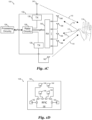
- Figure 1C illustrates a block diagram of sensor region 104 that includes radar front-end circuit 132 and processing circuitry 134.
- positions and gestures of target 114 may be detected by the sensor region 104.
- a gesture of two fingers tapping each other could be interpreted as a "button press," or a gesture of a rotating thumb and finger may be interpreted as turning a dial.
- target 114 is depicted in Figure 1C as being a hand
- sensor region 104 may also be configured to determine gestures and positions of other types of targets such as a human body, machinery and other types of animate or inanimate objects.
- Sensor region 104 may be implemented, for example, using a two-dimensional millimeter-wave (MMW) phase-array radar that measures the position and relative speed of target 114.
- MMW phase-array radar transmits and receives signals in the 50 GHz to 80 GHz range. Alternatively, frequencies outside of this range may also be used.
- radar front-end circuit 132 operates as a frequency modulated continuous wave (FMCW) radar sensor having multiple transmit and receive channels.
- FMCW frequency modulated continuous wave
- Radar front-end circuit 132 transmits and receives radio signals for detecting target 114 in three-dimensional space. For example, radar front-end circuit 132 transmits an incident RF signal and receives a RF signal that is a reflection of the incident RF signal from target 114. The received reflected RF signal is downconverted by radar front-end circuit 132 to determine beat frequency signals. These beat frequency signals may be used to determine information such as the location, speed, angle, etc., of target 114 in three-dimensional space.
- radar front-end circuit 132 is configured to transmit incident RF signals toward target 114 via transmit antennas 142 and to receive reflected RF signals from target 114 via receive antennas 144.
- Radar front-end circuit 132 includes transmitter front-end circuits 138 coupled to transmit antennas 142 and receiver front-end circuit 140 coupled to receive antennas 144.
- transmitter front-end circuits 138 may transmit RF signals toward target 114 one at a time or simultaneously. While two transmitter front-end circuits 138 are depicted in Figure 1C , it should be appreciated that radar front-end circuit 132 may include fewer or greater than two transmitter front-end circuits 138.
- Each transmitter front-end circuit 138 includes circuitry configured to produce the incident RF signals. Such circuitry may include, for example, RF oscillators, upconverting mixers, RF amplifiers, variable gain amplifiers, filters, transformers, power splitters, and other types of circuits.
- Receiver front-end circuit 140 receives and processes the reflected RF signals from target 114. As shown in Figure 1C , receiver front-end circuit 140 is configured to be coupled to four receive antennas 144, which may be configured as a 2 x 2 antenna array. In alternative embodiments, receiver front-end circuit 140 may be configured to be coupled to greater or fewer than four antennas, with the resulting antenna array being of various n ⁇ m dimensions depending on the specific embodiment and its specifications. Receiver front-end circuit 140 may include, for example, RF oscillators, upconverting mixers, RF amplifiers, variable gain amplifiers, filters, transformers, power combiners and other types of circuits.
- Radar circuitry 136 provides signals to be transmitted to transmitter front-end circuits 138, receives signals from receiver front-end circuit 140, and may be configured to control the operation of radar front-end circuit 132.
- radar circuitry 136 includes, but is not limited to, frequency synthesis circuitry, upconversion and downconversion circuitry, variable gain amplifiers, analog-to-digital converters, digital-to-analog converters, digital signal processing circuitry for baseband signals, bias generation circuits, and voltage regulators.
- Radar circuitry 136 may receive a baseband radar signal from processing circuitry 134 and control a frequency of an RF oscillator based on the received baseband signal.
- this received baseband signal may represent a FMCW frequency chip to be transmitted.
- Radar circuitry 136 may adjust the frequency of the RF oscillator by applying a signal proportional to the received baseband signal to a frequency control input of a phase locked loop.
- the baseband signal received from processing circuitry 134 may be upconverted using one or more mixers.
- Radar circuitry 136 may transmit and digitize baseband signals via a digital bus (e.g., a USB bus), transmit and receive analog signals via an analog signal path, and/or transmit and/or receive a combination of analog and digital signals to and from processing circuitry 134.
- a digital bus e.g., a USB bus
- Processing circuitry 134 acquires baseband signals provided by radar circuitry 136 and performs one or more signal processing steps to evaluate them. In an embodiment, processing circuitry 134 acquires a baseband signal that represents the beat frequency signals. The signal processing steps may include performing a fast Fourier transform (FFT), a short-time Fourier transform (STFT), target classification, machine learning, and the like. Results of the signal processing steps are used to determine and perform an action on the device, such as portable device 100 of Figure 1A . In addition to processing the acquired baseband signals, processing circuitry 134 may also control aspects of radar front-end circuit 132, such as the transmissions produced by radar front-end circuit 132.
- FFT fast Fourier transform
- STFT short-time Fourier transform
- processing circuitry 134 may also control aspects of radar front-end circuit 132, such as the transmissions produced by radar front-end circuit 132.
- radar front-end circuit 132 may be implemented on one or more RF integrated circuits (RFICs), antennas 142 and 144 may be disposed on a circuit board, and processing circuitry 134 may be implemented using a processor, a microprocessor, a digital signal processor and/or a custom logic circuit disposed on one or more integrated circuits/semiconductor substrates.
- Processing circuitry 134 may include a processor that executes instructions stored in a non-transitory memory to perform the functions of processing circuitry 134. In some embodiments, however, all or part of the functionality of processing circuitry 134 may be incorporated on the same integrated circuit/semiconductor substrate on which radar front-end circuit 132 is disposed.
- radar front-end circuit 132 may be implemented in a package that contains transmit antennas 142, receive antennas 144, transmitter front-end circuits 138, receiver front-end circuit 140, and/or radar circuitry 136.
- radar front-end circuit 132 may be implemented as one or more integrated circuits disposed on a circuit board, and transmit antennas 142 and receive antennas 144 may be implemented on the circuit board adjacent to the integrated circuits.
- transmitter front-end circuits 138, receiver front-end circuit 140, and radar circuitry 136 are formed on a same radar front-end integrated circuit (IC) die.
- IC radar front-end integrated circuit
- Transmit antennas 142 and receive antennas 144 may be part of the radar front-end IC die, or may be separate antennas over or adjacent to the radar front-end IC die.
- the radar front-end IC die may further include conductive layers, such as redistribution layers (RDLs), used for routing and/or for the implementation of various passive or active devices of radar front-end circuit 132.
- transmit antennas 142 and receive antennas 144 may be implemented using the RDLs of the radar front-end IC die.
- Figure 1D illustrates a plan view of radar system circuit 108 that includes radar front-end circuit 132 implemented as an RFIC coupled to transmit antennas 142 and receive antennas 144 implemented as patch antennas disposed on or within substrate 152.
- substrate 152 may be implemented using a circuit board on which radar front-end circuit 132 is disposed and on which transmit antennas 142 and receive antennas 144 are implemented using conductive layers of the circuit board.
- substrate 152 represents a wafer substrate on which one or more RDLs are disposed and on which transmit antennas 142 and receive antennas 144 are implemented using conductive layers on the one or more RDLs. It should be appreciated that the implementation of Figure 1D is just one of many ways that embodiment radar systems may be implemented.
- an electronic device may benefit from RF functionality such as radar functionality on one side of a device coupled to electronic circuitry located on a printed circuit board (PCB) on a second side of the device.
- a mobile phone may include a display such as a liquid crystal display (LCD) screen which displays an image at a front side of the device where RF functionality may be also be desired.
- LCD liquid crystal display
- an LCD screen may include an LCD stack containing a combination of transparent layers and RF-opaque layers such as polarizing filters, glass layers, liquid crystal layers, and reflector layers.
- RF-opaque layers such as polarizing filters, glass layers, liquid crystal layers, and reflector layers.
- MMW radar sensors may be unable to penetrate a metal reflector layer that is included in many LCD stacks.
- Other examples of an intervening RF-opaque layer may be a touch-sensing layer or a ground plane in an electronic device.
- a bezel including RF antennas may be included to allow transmission and reception of RF signals on the same side of the device as an LCD screen.
- a bezel may increase the size of the screen and therefore limit the compactness of the device. It may then be desirable to reduce the overall size of electronic devices such as mobile phones, tablet computers, laptop computers, computer monitors, televisions, vehicles, smartwatches, Internet of Things (IoT) device, etc. by improving integration of RF antennas with the LCD screen.
- IoT Internet of Things
- an RF system includes an antenna located on a first side of a substrate coupled to circuitry on a second side of the substrate.
- the first and second surfaces of the substrate may be opposing surfaces.
- the first and second surfaces may form a substantially 90° angle with one another.
- the antenna is operatively coupled to the circuitry using a flexible means such as a flexible substrate including a transmission line such as a flexible printed circuit (FPC) or a flexible connector such as a flat flexible cable (FFC).
- the flexible means is bent such that a first portion of the flexible means overlaps a first surface on the first side of the substrate and a second portion of the flexible means overlaps a second surface on the second side of the substrate.
- the antenna is configured to transmit and/or receive RF signals on the first side of the substrate.
- the substrate may include an RF-opaque layer such as a reflective layer in an LCD screen.
- the circuitry on the second side of the substrate may be located on a PCB.
- the PCB may be the primary PCB of a mobile phone or a tablet computer.
- RF signals and/or control signals may be sent from the first side to the second side using the flexible means.
- the RF system may advantageously enable a transparent layer such as a glass layer of an LCD screen to incorporate antenna functionality.
- antennas may be located on interior or exterior surfaces of the glass layer as well as integrated within the glass layer.
- System extension may be possible through integration of some or all of the RF functionality into a transparent substrate.
- the transparent substrate may be configured to improve performance of the antenna by increasing gain or shaping the radiation pattern of the antenna to better suit a particular application.
- an antenna may be integrated with an LCD screen at the front of an electronic device and coupled to an IC chip located on the back of the electronic device using a flexible substrate.
- the flexible substrate may be made thin and bent so that it is in close proximity to a side surface of the LCD stack of the LCD screen.
- the overall size of the electronic device may be advantageously reduced by decreasing the size of the bezel of the LCD screen while enabling RF functionality such as gesture control, ranging of objects, identification of obj ects, and motion tracking at the screen side of an electronic device.
- Embodiments provided below describe various structures and methods of forming an RF system, and in particular, RF systems that are integrated with display regions of an electronic device.
- the following description describes the embodiments as well as alternative examples.
- Various embodiment RF systems including a flexible substrate are described using Figures 3-5 and 6A-6C .
- Several alternative examples RF systems including a flexible connector and an integrated region are described using Figures 7, 8 , 9A, and 9B .
- Two alternative example RF systems including antennas integrated with a transparent substrate are described using Figures 10 and 11 .
- Four embodiment antennas are described using Figures 12-15 .
- Various embodiment RF systems including antennas located above an LCD screen are described using Figures 16-20 .
- An embodiment method of forming an RF system is described using Figure 21 .
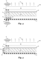
- Figure 2 illustrates a cross-sectional view of an alternative example RF system including an RF-opaque layer, one or more antennas, an IC chip, and a flexible substrate.
- an RF system 200 includes a first portion 81 of a flexible substrate 16 overlapping a first surface 88 of an RF-opaque layer 20, a second portion 83 overlapping a second surface 89 of the RF-opaque layer 20, and a bent region 82 between the first portion 81 and the second portion 83.
- the RF-opaque layer 20 may be any type of suitable substrate.
- RF-opaque layer 20 may be a stack of various layers configured for a specific functionality in an electronic device.
- the RF-opaque layer 20 may also include a metal support structure or a ground plane.
- RF-opaque layer 20 may be opaque to some or all electromagnetic signals in the RF frequency range.
- the RF frequency range may extend from about 3 kHz to about 300 GHz. However, the RF frequency range may also be considered to extend below 3 kHz and/or above 300 GHz depending on specific definitions within various areas of application.
- Flexible substrate 16 may be any type of suitable flexible substrate that is capable of being bent after formation or capable of being formed with a bent region. Any curvature imparted on the flexible substrate 16 may be implemented such that electronic components and circuitry located on the flexible substrate 16 remains functional.
- interconnects, transmission lines, and other electronic components may be formed on a flexible substrate 16 prior to a bending process. During the bending process a bent region 82 may be formed a such that the interconnects, transmission lines, and other electronic components maintain desired functionality.
- the flexible substrate 16 is an FPC. It should be noted that although a broad class of substrates may be considered FPCs, circuitry on an FPC is not required to be "printed" and may also be etched, formed in a lift-off process, etc.
- the flexible substrate 16 is a Pyralux ® PCB.
- the Pyralux ® PCB may be a single-layer, double-layer, or multi-layer flexible PCB including one or more copper foil layers bonded to one or more polyimide dielectric layers.
- flexible substrate 16 may include polyester dielectric layers.
- flexible substrate 16 may include one or more conductive materials such as copper (Cu), aluminum (Al), silver (Ag), gold (Au), or tungsten (W), as examples. Other suitable flexible substrates may be apparent to those of ordinary skill in the art.
- One or more antennas 40 are located above the first portion 81 of the flexible substrate 16.
- the antennas 40 may be operatively coupled to the first portion 81 of flexible substrate 16.
- Antennas 40 may include any type of suitable antenna and may be configured to transmit and/or receive RF signals 70. Additional antennas may be included above the first surface 88 as well as at other locations in the RF system 200.
- the antennas 40 may represent an array of antennas configured to track the movement of an object in three-dimensional space.
- the one or more antennas 40 may also include multiple antennas, some of which are configured only to transmit RF signals while others are configured only to receive RF signals.
- antennas 40 are implemented as planar antennas.
- antennas 40 may include a patch antenna, a tapered slot antenna (TSA), a Vivaldi antenna, a log periodic dipole antenna (LPDA), a quasi-Yagi antenna, a leaky wave antenna (LWA), or the like. Any suitable configuration may be chosen for the antennas 40 including patch, slot, ring, spiral, bow-tie configurations, or any other shape.
- the antennas 40 include an electrically conductive material.
- the antennas 40 include copper (Cu).
- the antennas 40 are situated such that at least a portion of one or more of the antennas 40 overlaps with the first surface 88.
- the antennas 40 are located directly above the first surface 88.
- the antennas 40 are attached directly to flexible substrate 16.
- the antennas 40 may be planar antennas formed on a Pyralux ® PCB. However, additional layers may be present between the first portion 81 of the flexible substrate 16 and the antennas 40.
- the antennas 40 may be located directly on the first surface 88 of RF-opaque layer 20 and the flexible substrate 16 may be operatively coupled to the antennas 40 using components on RF-opaque layer 20.
- the antennas 40 may be configured to transmit and/or receive RF signals 70 in the region directly above the first surface 88 of RF-opaque layer 20.
- RF signals 70 may include any RF frequency or band of RF frequencies.
- Dimensions of each of the antennas 40 may be related to desired frequency response of the RF system 200.
- the antennas 40 may be configured to operate in the MMW range of the RF spectrum.
- Such antennas 40 may each have a length and a width between 1 mm and 2.5 mm.
- each of the antennas 40 may have a length of about 1.5 mm and a width of about 850 ⁇ m.
- each of the antennas 40 may have a length of about 1.3 mm and a width of about 1.2 mm.
- the antennas 40 are not limited to these dimensions as a large number of factors may be considered when designing antennas. Therefore, a wide range of suitable dimensions not explicitly mentioned may be apparent to those of ordinary skill in the art.
- the RF system 200 further includes an IC chip 60 located below the second portion 83 of flexible substrate 16.
- IC chip 60 may be operatively coupled to the second portion 83 of flexible substrate 16 so that IC chip 60 is able to communicate with the antennas 40 using the bent region 82 of flexible substrate 16. Similar to the antennas 40, IC chip 60 is situated such that at least a portion of IC chip 60 overlaps with the second surface 89 of RF-opaque layer 20 and, in various examples, the entire IC chip 60 is located directly below the second surface 89.
- IC chip 60 may be directly attached to the second portion 83 of flexible substrate 16 or may have intervening layers.
- the IC chip 60 may include RF front end circuitry in addition to other circuitry and may be configured to process RF signals transmitted and received at the antennas 40 and is an RFIC in one example.
- IC chip 60 is configured to process the RF signals 70 by communicating with the antennas 40 using transmission lines located on flexible substrate 16.
- the IC chip 60 may have a receive interface connected to receiving antennas and/or a transmit interface connected to transmitting antennas. In some configurations, a receive interface and a transmit interface may be combined into a single interface.
- the RF front end circuitry is designed to operate in a super high frequency (SHF) or an extremely high frequency (EHF) regime.
- the IC chip 60 may contain MMW circuitry designed to operate in the unlicensed band from 57 GHz to 64 GHz. Additionally or alternatively, the IC chip 60 may contain circuitry designed to operate in the 28 GHz regime (in 5G applications, for example).
- IC chip 60 contains circuitry configured to operate in a frequency band including 77 GHz.
- automotive radar applications may utilize RF signals 70 that include 77 GHz. Other frequency bands are also possible.
- IC chip 60 may also contain circuitry designed to operate in frequency bands designated for other communication applications such as a global positioning system (GPS) network, global system for mobile communications (GSM) network, long-term evolution (LTE) network, worldwide interoperability for microwave access (WiMAX) networks, and/or industrial, scientific, and medical (ISM) band-based networks such as wireless local area networks (WLANs), Bluetooth, near field communication (NFC), etc.
- GPS global positioning system
- GSM global system for mobile communications
- LTE long-term evolution
- WiMAX worldwide interoperability for microwave access
- ISM industrial, scientific, and medical
- IC chip 60 includes a semiconductor substrate.
- the semiconductor substrate includes silicon.
- the semiconductor substrate includes silicon germanium (SiGe).
- the semiconductor substrate includes gallium arsenide (GaAs).
- Other suitable materials suitable for use as a substrate for IC chip 60 may be apparent to those of ordinary skill in the art.
- IC chip 60 may include additional components such as active and passive devices, metal layers, dielectric layers, doped and intrinsic semiconductor regions, redistribution layers, and other components known in the art. In various examples, IC chip 60 has already undergone back end of line (BEOL) processing before being coupled to flexible substrate 16.
- BEOL back end of line
- a possible advantage of examples in which the antennas 40 and IC chip 60 are fully overlapping respective surfaces of RF-opaque layer 20 may be to reduce the overall size of RF system 200.
- flexible substrate thickness 17 is between 100 ⁇ m and 500 ⁇ m. In one example, flexible substrate thickness 17 is about 150 ⁇ m. In another example, flexible substrate thickness 17 is about 200 ⁇ m.
- flexible substrate 16 may be bent so the bent region 82 is very close to a side surface of RF-opaque layer 20.
- the total width of the electronic device added by the bent region 82 of flexible substrate 16 may advantageously be kept very small.
- lateral dimensions of the antennas 40 may be much larger than flexible substrate thickness 17. Therefore, the total width added to implement equivalent antennas 40 adjacent to RF-opaque layer 20 rather than overlapping the first surface 88, would be much larger than examples using flexible substrate 16 or other suitable thin flexible means.
- Figure 3 illustrates a cross-sectional view of an example RF system including an LCD screen, antennas, an IC chip, and a flexible substrate in accordance with an embodiment of the invention.
- an RF system 300 includes antennas 40 located on a first side of an LCD screen 22 and an IC chip 60 located on an opposite second side of the LCD screen 22.
- the antennas 40 are operatively coupled to the IC chip 60 using a flexible substrate 16.
- the antennas 40 are configured to transmit and/or receive RF signals 70 on the first side of the LCD screen 22.
- RF system 300 may be a specific implementation of RF system 200 with similarly labeled elements being as previously described.
- RF system 300 may include a conductive layer 30 that is located above the LCD screen 22 on the first side.
- the conductive layer 30 is a touch sensing layer of a touch screen for an electronic device.
- the touch sensing layer may include conductive traces including driving lines and sensing lines configured to detect touch events input by a user.
- the conductive layer 30 may be RF-opaque due to the inclusion of conductive regions.
- the LCD screen 22 may be considered a specific implementation of the RF-opaque layer 20 shown in Figure 2 .
- LCD screen 22 may include a reflector layer which is RF-opaque.
- Other layers of the LCD screen 22 may also be RF-opaque.
- the combination of the LCD screen 22 and the conductive layer 30 may be considered a specific example of the RF-opaque layer 20 of Figure 2 .
- a ground plane region 32 is optionally included on the flexible substrate 16 on an opposite side of flexible substrate 16 as the antennas 40.
- the ground plane region 32 may be configured to prevent signals from passing between the antennas 40 and the LCD screen 22.
- the ground plane region 32 may also help to direct the RF signals 70 in a direction away from the LCD screen 22.
- a transparent layer 50 may be included above the LCD screen 22 and the conductive layer 30.
- transparent layer 50 includes a glass material.
- transparent layer 50 includes Gorilla ® Glass.
- the transparent layer 50 includes a plastic material.
- Other suitable transparent materials that may be used to implement transparent layer 50 may be apparent to those of ordinary skill in the art.
- the transparent layer 50 may be transparent or translucent to electromagnetic radiation.
- the transparent layer 50 may be transparent to visible light.
- Transparent layer 50 may also be transparent to RF signals.
- RF signals 70 may also be transmitted through transparent layer 50 on the same side of LCD screen 22 as the visible light 72.
- the IC chip 60 is coupled to the flexible substrate 16 using solder balls 62.
- the solder balls 62 may be part of a ball grid array (BGA) attachment method.
- BGA ball grid array
- a BGA and solder reflow process may be used to provide electrical and physical connections between the IC chip 60 and flexible substrate 16.
- IC chip 60 may be attached to flexible substrate 16 using any suitable attachment method including other surface mount technology (SMT) methods, wire bonding, conductive pillars, adhesive, and the like.
- SMT surface mount technology
- a PCB 12 is located below LCD screen 22 may be operatively coupled to IC chip 60.
- a first major surface of the IC chip 60 is attached to flexible substrate 16 while an opposing second major surface is attached to the PCB 12.
- the PCB 12 may include additional electronic devices, processors, memory, and the like.
- PCB 12 is a main board for an electronic device including radar system 300.
- the PCB 12 may be the main board for a mobile phone, smartwatch, laptop computer, IoT device, virtual reality headset, radar module in a vehicle, and the like.
- Figure 4 illustrates a cross-sectional view of an example RF system including front side and backside antennas, an LCD screen, an IC chip, and a flexible substrate in accordance with an embodiment of the invention.
- an RF system 400 includes a transparent substrate 50 located above an LCD screen 22 and a PCB 12 located below the LCD screen 22.
- the RF system 400 is configured to transmit and/or receive RF signals 70 through transparent substrate 50 as well as to transmit visible light 72 through transparent substrate 50.
- RF system 400 may be a specific implementation of RF system 300 with similarly labeled elements being as previously described.
- RF system 400 is further configured to transmit and/or receive second RF signals 76 on the PCB 12 side of the LCD screen 22.
- the RF signals 70 are transmitted and/or received by front side antennas 41 which may be a specific implementation of antenna 40 as illustrated in Figures 2 and 3 .
- the second RF signals 76 are transmitted and/or received by backside antennas 49 located on or within PBC 12.
- the front side antennas 41 and the backside antennas 49 are both operatively coupled to an IC chip 60.
- backside antennas 49 may be operatively couple to a separate IC chip located anywhere in RF system 400.
- RF system 400 may advantageously allow RF signals to be transmitted and received on both sides of LCD screen 22 without increasing the size of a device that includes RF system 400.
- a bezel may be added to one or more border regions of LCD screen 22 thereby undesirably increasing the size of the device.
- RF system 400 includes a thin, flexible substrate 16 enabling coupling of an IC chip 60 to antennas located directly above an LCD screen 22 beneficially allowing a device that may include RF system 400 to be smaller.
- Figure 5 illustrates a cross-sectional view of an example RF system including an IC chip oriented at a substantially 90° angle relative to a major surface of an LCD screen, antennas, and a flexible substrate in accordance with an embodiment of the invention.
- an RF system 500 includes a transparent substrate 50 located above an LCD screen 22 and a PCB 12 located below the LCD screen 22.
- the RF system 500 is configured to transmit and/or receive RF signals 70 through transparent substrate 50 as well as to transmit visible light 72 through transparent substrate 50.
- RF system 500 may be an alternative implementation of RF system 300 with similarly labeled elements being as previously described.
- an IC chip 60 included in RF system 500 is located along a side surface of an LCD screen 22 and is oriented at a substantially 90° angle relative to antennas 40 located above LCD screen 22.
- the IC chip 60 is attached to a flexible substrate 16 that is operatively coupled to the antennas 40 and a PCB 12.
- the configuration of RF system 500 may advantageously allow the thickness of a device including RF system 500 to be decreased by slightly increasing a dimension parallel to the face of the LCD screen. For example, the thickness of IC chip 60 and the solder balls 62 may be moved from below the LCD screen 22 to a side surface of the LCD screen 22 as shown.
- the thickness of IC chip 60 and a suitable attachment method may be chosen to be much smaller than the dimensions of a bezel for antennas that might be included along a border of an LCD screen. Therefore, the configuration of RF system 500 may beneficially allow the device to be thinner while still decreasing the size of the device including RF system 500 when compared to devices including a bezel for antennas.
- the location of IC chip 60 at a side of the LCD screen 20 may also advantageously reduce the distance from IC chip 60 to antennas 40.
- transmission lines on the flexible substrate 16 of RF system 500 may be shorter than those of the RF system 300.
- the reduced distance may beneficially reduce signal losses within the transmission lines.
- the IC chip 60 may be attached to the flexible substrate 16 at a substantially 90° angle relative to a major surface of the LCD screen similar to RF system 500. Such a configuration may enable an equal distance from the front side antennas 41 and backside antennas 49 to the IC chip 60.
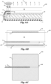
- Figure 6A illustrates a cross-sectional view of an example RF system including an antennas located on an outer surface of a transparent substrate, an LCD screen, an IC chip, and a flexible substrate in accordance with an embodiment of the invention
- Figure 6B illustrates a cross-sectional view of a portion of the RF system
- Figure 6C illustrates a bottom view of a portion of the RF system.
- an RF system 600 includes a transparent substrate 50 located above an LCD screen 22 and a PCB 12 located below the LCD screen 22.
- the RF system 600 is configured to transmit and/or receive RF signals 70 through transparent substrate 50 as well as to transmit visible light 72 through transparent substrate 50.
- RF system 600 may be an alternative implementation of RF system 500 with similarly labeled elements being as previously described.
- antennas 40 included in RF system 600 are located above the transparent substrate 50.
- the antennas 40 may be formed on the transparent substrate 50 by etching a conductive layer or using a direct structuring laser process and subsequent conductive material deposition, as examples.
- the antennas 40 may be formed during a PCD fabrication process.
- Transmission lines 34 located on a flexible substrate 16 are included to operatively couple an IC chip 60 to the antennas 40 through transparent substrate 50.
- one of the antennas 40 may be coupled to transmission lines 34 within a dashed region 86 as shown.
- Figure 6B shows a detailed view of the dashed region 86 of Figure 6A showing one of the antennas 40, a transmission line 34, flexible substrate 16, and ground plane region 32.
- a bottom view of the antenna 40 and transmission line 34 is shown in Figure 6C .
- the antenna 40 is a proximity coupled patch antenna, but any suitable antenna configuration may be used.
- the configuration of RF system 600 may advantageously enhance the bandwidth of the RF system 600 due to the dielectric constant of the transparent substrate 50.
- the transparent substrate may include a glass material with a high dielectric constant.
- the high dielectric constant of the glass material may enhance the bandwidth of antennas 40 located above transparent layer 50.
- integrated of antennas 40 with transparent substrate 50 may also advantageously allo9w integration of antennas 40 and IC chip 60 using standard packaging processes.
- Figure 7 illustrates a cross-sectional view of an alternative example RF system including a first PCB, an antenna coupled to circuitry on a second PCB using an integrated region within a transparent substrate, an LCD screen, and a flexible connector.
- an RF system 700 includes a transparent substrate 50 located above an LCD screen 22 and a PCB 12 located below the LCD screen 22.
- the RF system 700 is configured to transmit and/or receive RF signals 70 through transparent substrate 50 as well as to transmit visible light 72 through transparent substrate 50.
- RF system 700 may be an alternative implementation of RF system 600 with similarly labeled elements being as previously described.
- RF system 700 includes a first PCB 13 located below the LCD screen 22 and a second PCB 14 located above the LCD screen 22.
- a flexible connector 18 is included to operatively couple the first PCB 13 to the second PCB 14 which is in turn operatively coupled to an antenna 40 located above the transparent substrate 50 using an integrated region 54.
- the integrated region 54 may include conductive layers and insulating layers that are structured as ground planes regions, interconnects, transmission lines, vias, contact pads, IC chips, and the like.
- the first PCB 13 and/or the second PCB 14 may include circuitry and or IC chips configured to process the RF signals 70 transmitted and/or received by the antenna 40.
- the flexible connector 18 is configured to couple the antenna 40 to the first PCB 13 located on the opposite side if LCD screen 22 similar to the flexible substrate 16 of other examples.
- Flexible connector 18 may be any suitable type of flexible connector. In one example, flexible connector 18 is an FFC.
- Figure 8 illustrates a cross-sectional view of an alternative example RF system including a first PCB, an antenna coupled to an IC chip located on a second PCB using an integrated region within a transparent substrate, an LCD screen, and a flexible connector.
- an RF system 800 includes a transparent substrate 50 located above an LCD screen 22 and a PCB 12 located below the LCD screen 22.
- the RF system 800 is configured to transmit and/or receive RF signals 70 through transparent substrate 50 as well as to transmit visible light 72 through transparent substrate 50.
- RF system 800 may be a specific implementation of RF system 700 with similarly labeled elements being as previously described.
- An IC chip 60 is included on the second PCB 14 operatively coupled to an antenna 40 located above the transparent substrate 50 using an integrated region 55.
- the IC chip 60 is configured to process the RF signals 70 on the same side of the LCD screen 22 as the side that the RF signals 70 are transmitted and/or received.
- the integrated region 55 may include a variety of elements such as ground plane regions and transmission lines, as examples.
- Figure 9A illustrates a cross-sectional view of an alternative example RF system including a first PCB, antennas coupled to circuitry on a second PCB using an integrated region within a transparent substrate, an LCD screen, and a flexible connector
- Figure 9B illustrates a cross-sectional view of a portion of the RF system including the antennas, a ground plane region, and an IC chip integrated with the transparent substrate in the integrated region.
- an RF system 900 includes a transparent substrate 50 located above an LCD screen 22 and a PCB 12 located below the LCD screen 22.
- the RF system 900 is configured to transmit and/or receive RF signals 70 through transparent substrate 50 as well as to transmit visible light 72 through transparent substrate 50.
- RF system 900 may be a specific implementation of RF system 700 with similarly labeled elements being as previously described.
- RF system 900 includes an integrated region 56 through which one or more antennas 40 are operatively coupled to an IC chip 60 located within the integrated region 56, a first PCB 13 located below the LCD screen 22, and a second PCB 14 located above the LCD screen 22.
- Electrical contacts 38 couple to integrated region 56 to the second PCB 14.
- a first transparent layer 51 is located above the electrical contacts 38.
- a ground plane region 38 is located above transparent layer 51 and is connected to one or more of the electrical contacts 38 using one or more vias 35.
- the IC chip 60 is located within the first transparent layer 51 and is coupled to the one or more of the electrical contacts 38 as well as the antennas 40 using transmission lines (not shown) in the same layer as the ground plane region 36.
- a second transparent layer 52 is located above the ground plane region 36.
- the antennas 40 are located above the second transparent layer 52.
- the combination of the first transparent layer 51 and the second transparent layer 52 make up transparent layer 50.
- one or both of the first transparent layer 51 and the second transparent layer 52 are glass.
- the first transparent layer 51 and the second transparent layer 52 are Gorilla ® Glass.
- the number of layers included in the integrated region 56 may depend on specific design considerations and desired functionality.
- the integrated region 56 may include two transparent layers as shown in Figures 9A and 9B or may include four transparent layers. In other examples, other numbers of layers may be included in integrated region 56.
- the RF system 900 may advantageously reduce the thickness of a device including the RF system 900 by integrating the IC chip 60 into transparent layer 50. As a result the overall thickness of the device may beneficially be reduced by an amount approximately equal to the thickness of the IC chip 60. Additionally, configurations of RF systems with antennas on a top surface of the transparent layer such as RF systems 600, 700, 800, and 900 may provide additional benefits to the gain of the RF system.
- Figure 10 illustrates a cross-sectional view of an alternative example RF system including a parasitic antenna located on a top surface of a transparent substrate, an antenna located at a bottom surface of the transparent substrate, and an IC chip.
- an RF system 1000 includes an IC chip 60 including an antenna 40 located below a transparent substrate 50 and a parasitic antenna 48 located above the transparent substrate 50.
- the transparent substrate 50, IC chip 60, and parasitic antenna 48 of RF system 1000 may be a specific antenna configuration usable with any of the RF systems as described herein with similarly labeled elements being as previously described.
- the parasitic antenna 48 may be operatively coupled to the antenna 40 through transparent substrate 50.
- a ground plane region 36 may be optionally included in IC chip 60 and may be configured to direct electromagnetic radiation in appropriate directions within IC chip 60.
- IC chip 60 is an RFIC.
- IC chip 60 is an RF package including an RFIC.
- RF front end circuitry may be included in IC chip 60 below ground plane region 36. The RF front end circuitry may be configured to process RF signals 70 and may be coupled to the antenna 40 using transmission lines within IC chip 60.
- Antenna 40 may radiate RF signals that excite the parasitic antenna 48 causing it to radiate RF signals 70.
- RF signals 70 received at the parasitic antenna 48 may excite the antenna 40 which may then allow reception of RF signals 70 at the RF front end circuitry.
- Figure 11 illustrates a cross-sectional view of an alternative example RF system including a shaped transparent region located above an antenna and an IC chip where the antenna and the IC chip are integrated with a transparent substrate.
- an RF system 1100 includes an IC chip 60 including an antenna 40 and an optional ground plane region 36 located within a transparent substrate 50 and a shaped transparent region 58 located above the transparent substrate 50.
- the transparent substrate 50, IC chip 60, and shaped transparent region 58 of RF system 1100 may be a specific antenna configuration usable with any of the RF systems as described herein with similarly labeled elements being as previously described.
- the shaped transparent region 58 may be configured to function as an RF lens for RF signals 70 that are transmitted and/or received by antenna 40.
- the desired field of view of antenna 40 may be in a specific, localized region above transparent substrate 50.
- the radiation pattern of RF signals 70 may be much broader than desired for the desired application.
- the shaped transparent region 58 may advantageously focus RF signals 70 to be predominantly radiated in a specifically defined region above transparent substrate 50.
- the radiation pattern of antenna 40 may be too focused for a specific application.
- shaped transparent region 58 may broaden and homogenize the RF signals 70 in the region above transparent substrate 50.
- the signal strength of RF signals 70 may be substantially similar at all points at a specified distance above transparent substrate 50.
- Figures 12-15 illustrate example antennas in accordance with embodiments of the invention usable in RF systems as described herein.
- Figure 12 illustrates a top view of a dipole antenna 92 including transmission lines 34 located on a transparent substrate 50.
- Figure 13 illustrates a top view of a patch antenna 94 including a transmission line 34 located on a transparent substrate 50.
- Figure 14 illustrates a bottom view of a proximity coupled patch antenna 96 located on a top surface of a transparent substrate 50 and a transmission line 34 located on an opposite bottom surface of the transparent substrate.
- Figure 15 illustrates a top view of a magneto-electric dipole antenna 98 located on a transparent substrate 50.
- any of the antennas in the embodiment RF systems described herein may be implemented using the example antennas illustrated in Figures 12-15 .
- the antennas 40 of RF system 300 may be implemented as patch antennas similar to the patch antenna 94 as illustrated in Figure 13 .
- the antennas 40 of RF system 600 may be implemented as proximity coupled patch antennas similar to the proximity coupled patch antenna 96 as illustrated in Figure 14 .
- the RF systems are not limited to the antenna configurations explicitly shown and described. Any suitable antenna configuration as apparent to one of ordinary skill in the art may be used to implement any of the antennas in the RF systems described herein.
- Figure 16 illustrates a top view of an example RF system including a transmit antenna and a receive antenna centrally located in a top region of an LCD screen in accordance with an embodiment of the invention.
- an RF system 1600 includes a transmit antenna 42 and a receive antenna 43 located directly above an LCD screen 22.
- the LCD screen 22 may be an LCD screen of a mobile device.
- the LCD screen 22 may be the LCD screen of other electronic devices that include RF system 1600.
- the LCD screen 22 as illustrated here is rectangular in shape, any suitable shape is possible and may depend on the specific type of electronic device or a particular application.
- Transmit antenna 42 and receive antenna 43 are configured to transmit and/or receive RF signals in a region directly above the LCD screen 22.
- transmit antenna 42 and receive antenna 43 are configured as a bistatic radar system.
- two or more antennas may be configured so that a subset of the two or more antennas are configured to only transmit RF signals while the remaining antennas are configured only to receive RF signals.
- additional antennas may be incorporated in the region directly above the LCD screen 22.
- transmit antenna 42 and receive antenna 43 may be replaced with a single antenna configured as a monostatic radar antenna that both transmits and receives RF signals.
- Figure 17 illustrates a top view of another example RF system including four antennas located at the corners of an LCD screen in accordance with an embodiment of the invention.
- an RF system 1700 includes four antennas 40 located at the corners and in a region directly above an LCD screen 22.
- the antennas 40 may be configured as individual monostatic radar antennas. In this configuration, RF signals transmitted and received at each of the antennas 40 may be processed individually. This may be referred to as non-coherent signal processing. In other embodiments, some or all of the antennas 40 may be configured to operate as a unified radar system using coherent signal processing. Additional antennas may be located around the edges of the LCD screen 22. In some embodiments, fewer than four of the corners of the LCD screen 22 may have an antenna. For example, in one alternative embodiment, only two antennas 40 may be located in the left two corners of LCD screen 22. These two corners may be the top corners of a mobile device, for example.
- Figure 18 illustrates a top view of an example RF system including an antenna region configured for cellular communication integrated with a transparent substrate located above an LCD screen in accordance with an embodiment of the invention.
- an RF system 1800 includes a communication antenna 44 integrated with a transparent substrate 50.
- communication antenna 44 may be etched onto a surface of transparent substrate 50.
- communication antenna 44 may be integrated within transparent substrate 50.
- communication antenna 44 includes multiple antenna regions configured for communication with networks using multiple communications standards such as GPS, GSM, LTE, Wi-Fi, Bluetooth, and the like.
- communication antenna 44 does not extend entirely around the border of the transparent substrate 50.
- An LCD screen as previously described may be located below transparent substrate 50 which is configured as a display surface for an electronic device.
- Figure 19 illustrates a top view of an example RF system including two communication antennas configured for cellular communication integrated with a transparent substrate located above an LCD screen in accordance with an embodiment of the invention.
- an RF system 1900 includes a first communications antenna 45 and a second communications antenna 46 integrated with a transparent substrate 50.
- the first communication antenna 45 is configured to communicate using a first communication standard while the second communication antenna 46 is configured to communicate using a different communication standard.
- the first communication antenna 45 is configured to communicate with an LTE network while the second communication antenna 46 is configured to communicate with a GSM network.
- the first communication antenna 45 is configured to communicate with an Wi-Fi network while the second communication antenna 46 is configured to communicate using a LTE network.
- Figure 20 illustrates a top view of an example RF system including two communication antennas configured for cellular communication and two antennas configured for radar applications integrated with a transparent substrate located above an LCD screen in accordance with an embodiment of the invention.
- an RF system 2000 includes a transmit antenna 42, a receive antenna 43, a first communication antenna 45, and a second communication antenna 46 integrated with a transparent substrate 50.
- the transmit antenna 42 and the receive antenna 43 may be part of a bistatic radar system as in RF system 1600 described previously in reference to Figure 16 . More or fewer antennas may be included and may depend on the specific type of device and particular application.
- RF systems 1600, 1700, 1800, 1900, and 2000 may be top views for RF systems of any other embodiment described herein.
- RF system 2000 may be a top view of a specific implementation of the RF system 600 that includes a bistatic radar system located at the top of an LCD screen of a mobile device while also including an LTE antenna and a Wi-Fi antenna located on the bordering sides and bottom of the LCD screen.
- RF system 1800 may be a top view of a specific implementation of the RF system 700 that includes several communication antennas integrated with a glass display screen of a tablet computer.
- Figure 21 illustrates a method of forming an RF system in accordance with an embodiment of the invention.
- a method 2100 of forming an RF system includes a step 2102 of providing a flexible substrate.
- the flexible substrate may include one or more conductive layers and one or more laminate layers and may be a flexible PCB in some embodiments.
- the flexible substrate is a Pyralux ® PCB.
- the method 2100 further includes a step 2104 of forming one or more antennas overlapping a first portion of the flexible substrate.
- the antennas may be formed on a first portion of the flexible substrate by etching a conductive layer on a surface of the flexible substrate.
- there may be additional layers such as one or more transparent layers between the first portion of the flexible substrate and the antennas.
- the antennas may be formed on a surface of the additional layers overlapping the first portion of the flexible substrate.
- the antennas may be formed using any suitable method such as etching, lift-off, printing, and the like.
- the method 2100 further includes a step 2106 of forming one or more transmission lines in a middle region of the flexible substrate between the first portion and a second portion of the flexible substrate.
- the transmission lines as well as additional circuitry may be formed in the middle region using any suitable method in a step 2106 separately from step 2104.
- step 2104 and step 2106 may be combined into a single step and the transmission lines, antennas, and other circuitry located on the flexible substrate may be formed in the same step.
- circuitry may also be formed at the second portion of the flexible substrate so that the second portion may be electrically coupled to additional circuitry located apart from the flexible substrate.
- the method 2100 further includes a step 2108 of attaching an IC chip to the second portion of the flexible substrate.
- the IC chip may be attached using any suitable method such as a BGA using solder reflow process, for example.
- the method 2100 further includes a method 2110 of attaching the first portion of the flexible substrate to a first surface of another substrate.
- the other substrate may be a planar substrate and may be RF-opaque.
- the other substrate is an LCD screen and is configured to display an image by transmitting visible light on the same side as the antennas.
- the method 2100 also includes a step 2112 of bending the middle region of the flexible substrate to form a bent region.
- the bent region may allow the second portion of the flexible substrate to overlap with a second surface of the other substrate opposite the first surface.
- the bent region may allow the flexible substrate to be attached in a step 2114 of attaching the second portion of the flexible substrate to the second surface of the other substrate.
- the IC chip overlapping the second surface is configured to process RF signals at the second surface that are transmitted and/or received by the antennas at the opposite first surface.
- steps of attaching a transparent substrate and a PCB overlapping the first and second surfaces of the other substrate respectively may be added when forming any of the RF systems including a transparent substrate and a PCB such as RF system 300.
Landscapes
- Engineering & Computer Science (AREA)
- Radar, Positioning & Navigation (AREA)
- Remote Sensing (AREA)
- Physics & Mathematics (AREA)
- Computer Networks & Wireless Communication (AREA)
- General Physics & Mathematics (AREA)
- General Engineering & Computer Science (AREA)
- Theoretical Computer Science (AREA)
- Computer Hardware Design (AREA)
- Electromagnetism (AREA)
- Human Computer Interaction (AREA)
- Signal Processing (AREA)
- Microelectronics & Electronic Packaging (AREA)
- Details Of Aerials (AREA)
- Support Of Aerials (AREA)
- Telephone Set Structure (AREA)
- Transceivers (AREA)
Claims (10)
- Hochfrequenzsystem, HF-System, (500; 600), Folgendes umfassend:ein flexibles Substrat (16), das Folgendes umfassteinen ersten Abschnitt (81), der eine erste Oberfläche (88) eines Substrats (22) des HF-Systems überlappt, wobei die erste Oberfläche (88) auf einer ersten Seite des HF-Systems ist, undeinen zweiten Abschnitt (83), der die zweite Oberfläche (89) des Substrats (22) überlappt, wobei die zweite Oberfläche (89) auf einer zweiten Seite des HF-Systems ist;wobei die erste Oberfläche (88) in einem im Wesentlichen rechten Winkel in Bezug zu der zweiten Oberfläche (89) ist;eine Antenne (40), die über dem ersten Abschnitt (81) des flexiblen Substrats (16) angeordnet ist, wobei die Antenne (40) eingerichtet ist, um HF-Signale auf der ersten Seite des HF-Systems (500; 600) zu senden/empfangen;eine Sendeleitung (34), die auf einem gebogenen Bereich (82) des flexiblen Substrats (16) zwischen dem ersten Abschnitt (81) und dem zweiten Abschnitt (83) angeordnet ist, wobei die Sendeleitung (34) eingerichtet ist, um die HF-Signale zwischen dem ersten Abschnitt (81) und dem zweiten Abschnitt (83) auf der zweiten Seite des HF-Systems (500; 600) weiterzuleiten; undeinen integrierten Schaltungschip, IS-Chip, (60), der an dem zweiten Abschnitt (83) des flexiblen Substrats (16) befestigt ist und unter Verwendung der Sendeleitung (34) wirksam an die Antenne (40) angeschlossen ist, wobei der IS-Chip (60) einen HF-Schaltkomplex umfasst, der eingerichtet ist, um die HF-Signale auf der zweiten Seite des HF-Systems (500; 600) zu verarbeiten,wobei das Substrat (22) HF-undurchlässig ist und eingerichtet ist, um sichtbares Licht an die erste Oberfläche (88) des Substrats (22) zu senden.
- Hochfrequenzsystem, HF-System, (300; 400), Folgendes umfassend:ein flexibles Substrat (16), das Folgendes umfassteinen ersten Abschnitt (81), der eine erste Oberfläche (88) eines Substrats (22) des HF-Systems überlappt, wobei die erste Oberfläche (88) auf einer ersten Seite des HF-Systems ist, undeinen zweiten Abschnitt (83), der die zweite Oberfläche (89) des Substrats (22) überlappt, wobei die zweite Oberfläche (89) auf einer zweiten Seite des HF-Systems ist;wobei die erste Oberfläche (88) der zweiten Oberfläche (89) entgegengesetzt ist;eine Antenne (40), die über dem ersten Abschnitt (81) des flexiblen Substrats (16) angeordnet ist, wobei die Antenne (40) eingerichtet ist, um HF-Signale auf der ersten Seite des HF-Systems (300; 400) zu senden/empfangen;eine Sendeleitung (34), die auf einem gebogenen Bereich (82) des flexiblen Substrats (16) zwischen dem ersten Abschnitt (81) und dem zweiten Abschnitt (83) angeordnet ist, wobei die Sendeleitung (34) eingerichtet ist, um die HF-Signale zwischen dem ersten Abschnitt (81) und dem zweiten Abschnitt (83) auf der zweiten Seite des HF-Systems (300; 400) weiterzuleiten; undeinen integrierten Schaltungschip, IS-Chip, (60), der an dem zweiten Abschnitt (83) des flexiblen Substrats (16) befestigt ist und unter Verwendung der Sendeleitung (34) wirksam an die Antenne (40) angeschlossen ist, wobei der IS-Chip (60) einen HF-Schaltkomplex umfasst, der eingerichtet ist, um die HF-Signale auf der zweiten Seite des HF-Systems (300; 400) zu verarbeiten,wobei das Substrat (22) HF-undurchlässig ist und eingerichtet ist, um sichtbares Licht an die erste Oberfläche (88) des Substrats (22) zu senden;eine Leiterplatte (12), die über der zweiten Oberfläche (89) des Substrats (22) angeordnet ist; undeine erste Hauptfläche des IS-Chips (60) an dem flexiblen Substrat (16) befestigt ist, wobei eine entgegengesetzte zweite Hauptfläche des IS-Chips (60) an der Leiterplatte (12) befestigt ist.
- HF-System (300; 400; 500) nach Anspruch 1 oder 2, weiterhin ein durchsichtiges Substrat (50) umfassend, das über der ersten Oberfläche (88) des Substrats (22) angeordnet ist, wobeidie Antenne (40) zwischen dem durchsichtigen Substrat (50) und dem Substrat (22) angeordnet ist unddie Antenne (40) weiterhin eingerichtet ist, um die HF-Signale durch das durchsichtige Substrat (50) zu senden/empfangen.
- HF-System (600) nach Anspruch 1 oder 2, weiterhin ein durchsichtiges Substrat (50) umfassend, das über der ersten Oberfläche (88) des Substrats (22) angeordnet ist, wobeidie Antenne (40) an einer oberen Oberfläche des durchsichtigen Substrats (50) befestigt ist,die Sendeleitung (34) mit einer unteren Oberfläche des durchsichtigen Substrats (50) überlappt, wobei die untere Oberfläche der oberen Oberfläche entgegengesetzt ist, unddie Antenne (40) durch das durchsichtige Substrat (50) elektromagnetisch an die Sendeleitung (34) angeschlossen ist.
- HF-System (500; 600) nach Anspruch 1 oder nach Anspruch 3 oder 4, wenn er sich auf Anspruch 1 bezieht, weiterhin Folgendes umfassend:
eine Leiterplatte (12), die über der zweiten Oberfläche (89) des Substrats (20; 22) angeordnet ist. - Verfahren zum Herstellen eines Hochfrequenzsystems, HF-Systems, (500; 600), das Verfahren Folgendes umfassend:Ausbilden einer Antenne (40), die einen ersten Abschnitt (81) eines flexiblen Substrats (16) überlappt;Ausbilden einer Sendeleitung (34) auf einem mittleren Bereich des flexiblen Substrats (16) zwischen dem ersten Abschnitt (81) und einem zweiten Abschnitt (83) des flexiblen Substrats (16);Befestigen des ersten Abschnitts (81) an einer ersten Oberfläche (88) eines Substrats (22), wobei das Substrat (22) HF-undurchlässig ist und eingerichtet ist, um sichtbares Licht an die erste Oberfläche (88) des Substrats (22) zu senden;Biegen des mittleren Bereichs des flexiblen Substrats (16), um einen gebogenen Bereich (82) des flexiblen Substrats (16) auszubilden; undBefestigen des zweiten Abschnitts (83) an einer zweiten Oberfläche (89) des Substrats (22), wobeidie Antenne (40) eingerichtet ist, um HF-Signale an der ersten Oberfläche (88) zu senden/empfangen.die Sendeleitung (34) eingerichtet ist, um die HF-Signale zwischen dem ersten Abschnitt (81) und dem zweiten Abschnitt (83) an der zweiten Oberfläche (89) des Substrats (22) weiterzuleiten, unddie erste Oberfläche (88) in einem im Wesentlichen rechten Winkel in Bezug zu der zweiten Oberfläche (89) ist; undBefestigen eines integrierten Schaltungschips, IS-Chips, (60), der einen HF-Schaltkomplex umfasst, an dem zweiten Abschnitt (83), wobei der IS-Chip (60) unter Verwendung der Sendeleitung (34) wirksam an die Antenne (40) angeschlossen ist, wobei der HF-Schaltkomplex eingerichtet ist, um die HF-Signale an der zweiten Oberfläche (89) zu verarbeiten.
- Verfahren zum Herstellen eines Hochfrequenzsystems, HF-Systems, (300; 400), das Verfahren Folgendes umfassend:Ausbilden einer Antenne (40), die einen ersten Abschnitt (81) eines flexiblen Substrats (16) überlappt;Ausbilden einer Sendeleitung (34) auf einem mittleren Bereich des flexiblen Substrats (16) zwischen dem ersten Abschnitt (81) und einem zweiten Abschnitt (83) des flexiblen Substrats (16);Befestigen des ersten Abschnitts (81) an einer ersten Oberfläche (88) eines Substrats (22), wobei das Substrat (22) HF-undurchlässig ist und eingerichtet ist, um sichtbares Licht an die erste Oberfläche (88) des Substrats (22) zu senden;Biegen des mittleren Bereichs des flexiblen Substrats (16), um einen gebogenen Bereich (82) des flexiblen Substrats (16) auszubilden; undBefestigen des zweiten Abschnitts (83) an einer zweiten Oberfläche (89) des Substrats (22), wobeidie Antenne (40) eingerichtet ist, um HF-Signale an der ersten Oberfläche (88) zu senden/empfangen.die Sendeleitung (34) eingerichtet ist, um die HF-Signale zwischen dem ersten Abschnitt (81) und dem zweiten Abschnitt (83) an der zweiten Oberfläche (89) des Substrats (22) weiterzuleiten, unddie erste Oberfläche (88) der zweiten Oberfläche (89) entgegengesetzt ist;Befestigen eines integrierten Schaltungschips, IS-Chips, (60), der einen HF-Schaltkomplex umfasst, an dem zweiten Abschnitt (83), wobei der IS-Chip (60) unter Verwendung der Sendeleitung (34) wirksam an die Antenne (40) angeschlossen ist, wobei der HF-Schaltkomplex eingerichtet ist, um die HF-Signale an der zweiten Oberfläche (89) zu verarbeiten; undBefestigen einer Leiterplatte (12) über der zweiten Oberfläche (89) des Substrats (22),wobei eine erste Hauptfläche des IS-Chips (60) an dem flexiblen Substrat (16) befestigt ist, wobei eine entgegengesetzte zweite Hauptfläche des IS-Chips (60) an der Leiterplatte (12) befestigt ist.
- Verfahren nach Anspruch 6 oder 7, weiterhin Befestigen eines durchsichtigen Substrats (50) über der ersten Oberfläche (88) des Substrats (22) umfassend, wobeiAusbilden einer Antenne (40) Ausbilden der Antenne (40) auf dem ersten Abschnitt (81) des flexiblen Substrats (16) zwischen dem durchsichtigen Substrat (50) und dem Substrat (22) umfasst unddie Antenne (40) weiterhin eingerichtet ist, um die HF-Signale durch das durchsichtige Substrat (50) zu senden/empfangen.
- Verfahren nach Anspruch 6 oder 7, weiterhin Befestigen eines durchsichtigen Substrats (50) über der ersten Oberfläche (88) des Substrats (22) umfassend, wobeiAusbilden einer Antenne (40) Ausbilden der Antenne (40) auf einer oberen Oberfläche des durchsichtigen Substrats (50) umfasst,die Sendeleitung (34) mit einer unteren Oberfläche des durchsichtigen Substrats (50) überlappt, wobei die untere Oberfläche der oberen Oberfläche entgegengesetzt ist, unddie Antenne (40) durch das durchsichtige Substrat (50) elektromagnetisch an die Sendeleitung (34) angeschlossen ist.
- Verfahren nach Anspruch 6 oder nach Anspruch 8 oder 9, wenn er sich auf Anspruch 6 bezieht, weiterhin Befestigen einer Leiterplatte (12) über der zweiten Oberfläche (89) des Substrats (22) umfassend.
Applications Claiming Priority (1)
| Application Number | Priority Date | Filing Date | Title |
|---|---|---|---|
| US15/782,288 US10775490B2 (en) | 2017-10-12 | 2017-10-12 | Radio frequency systems integrated with displays and methods of formation thereof |
Publications (3)
| Publication Number | Publication Date |
|---|---|
| EP3471197A2 EP3471197A2 (de) | 2019-04-17 |
| EP3471197A3 EP3471197A3 (de) | 2019-07-03 |
| EP3471197B1 true EP3471197B1 (de) | 2023-08-02 |
Family
ID=63720563
Family Applications (1)
| Application Number | Title | Priority Date | Filing Date |
|---|---|---|---|
| EP18197938.6A Active EP3471197B1 (de) | 2017-10-12 | 2018-10-01 | Hochfrequenzsysteme mit integrierten anzeigen und verfahren zur formung davon |
Country Status (3)
| Country | Link |
|---|---|
| US (2) | US10775490B2 (de) |
| EP (1) | EP3471197B1 (de) |
| CN (1) | CN109669511A (de) |
Families Citing this family (39)
| Publication number | Priority date | Publication date | Assignee | Title |
|---|---|---|---|---|
| US10775490B2 (en) | 2017-10-12 | 2020-09-15 | Infineon Technologies Ag | Radio frequency systems integrated with displays and methods of formation thereof |
| FR3075484B1 (fr) * | 2017-12-18 | 2021-10-15 | Sagemcom Broadband Sas | Antenne pour circuit imprime, circuit electronique et equipement electronique pourvus d'une telle antenne |
| US11016574B2 (en) * | 2018-10-31 | 2021-05-25 | Rogers Corporation | Millimeter-wave-radar-based electromagnetic apparatus |
| US11445929B2 (en) * | 2018-12-18 | 2022-09-20 | Movano Inc. | Systems for radio wave based health monitoring that utilize amplitude and phase data |
| US10649585B1 (en) * | 2019-01-08 | 2020-05-12 | Nxp B.V. | Electric field sensor |
| US11545733B2 (en) * | 2019-02-20 | 2023-01-03 | Samsung Electronics Co., Ltd. | Antenna module including flexible printed circuit board and electronic device including the antenna module |
| US12131693B2 (en) * | 2019-04-09 | 2024-10-29 | Motorola Mobility Llc | Electronic device with optically pellucid electrical conductor and systems and methods for compensating for the same |
| US11439003B2 (en) * | 2019-04-12 | 2022-09-06 | Samsung Electronics Co., Ltd. | Antenna module including printed circuit board and base station including the antenna module |
| CN110034375A (zh) * | 2019-04-19 | 2019-07-19 | Oppo广东移动通信有限公司 | 天线模组及电子设备 |
| CN110312009B (zh) * | 2019-06-26 | 2021-03-02 | 维沃移动通信有限公司 | 一种显示模组及移动终端 |
| CN110324055B (zh) * | 2019-06-28 | 2022-02-01 | 维沃移动通信有限公司 | 一种终端设备 |
| CN112234362B (zh) * | 2019-06-30 | 2022-03-01 | Oppo广东移动通信有限公司 | 壳体组件、天线组件及电子设备 |
| CN112186354A (zh) * | 2019-07-03 | 2021-01-05 | 华为技术有限公司 | 一种天线及终端设备 |
| KR102633997B1 (ko) | 2019-07-12 | 2024-02-05 | 엘지디스플레이 주식회사 | 안테나를 포함하는 표시장치 및 그 제조방법 |
| KR102137093B1 (ko) * | 2019-08-05 | 2020-07-23 | 삼성전기주식회사 | 안테나 모듈 및 이를 포함하는 전자기기 |
| CN113140194B (zh) | 2020-01-17 | 2023-08-29 | 北京小米移动软件有限公司 | 亮度调节方法、装置及存储介质 |
| EP4080680A4 (de) * | 2020-02-03 | 2024-01-17 | Agc Inc. | Antennenvorrichtung |
| CA3163808A1 (en) * | 2020-02-07 | 2021-08-12 | Alicia Droge | Glazing having an rfid transponder |
| DE102020203970A1 (de) * | 2020-03-26 | 2021-09-30 | Fraunhofer-Gesellschaft zur Förderung der angewandten Forschung eingetragener Verein | Hochfrequenzanordnung mit einer vorderseitigen und einer rückseitigen Antenne |
| KR102781246B1 (ko) * | 2020-04-28 | 2025-03-12 | 동우 화인켐 주식회사 | 안테나 패키지 및 이를 포함하는 화상 표시 장치 |
| CN111916885A (zh) * | 2020-06-15 | 2020-11-10 | 上海创功通讯技术有限公司 | 一种双频wifi pcb天线及终端设备 |
| US11831090B2 (en) * | 2020-06-16 | 2023-11-28 | Apple Inc. | Electronic devices with display-overlapping antennas |
| KR20220009207A (ko) * | 2020-07-15 | 2022-01-24 | 삼성전기주식회사 | 고주파 모듈을 포함하는 전자 기기 |
| EP3964864A1 (de) * | 2020-09-07 | 2022-03-09 | Infineon Technologies AG | Elektronische vorrichtung und verfahren für elektronische vorrichtung |
| CA3180277A1 (en) * | 2020-09-23 | 2022-03-31 | Thomas HOLTSTIEGE | Insulating glazing unit and glazing |
| KR102864025B1 (ko) | 2020-10-05 | 2025-09-25 | 삼성디스플레이 주식회사 | 전자 장치 |
| US11682842B1 (en) * | 2020-10-08 | 2023-06-20 | Rockwell Collins, Inc. | Log periodic array application of minature active differential/quadrature radiating elements |
| KR102833066B1 (ko) * | 2020-10-14 | 2025-07-15 | 삼성디스플레이 주식회사 | 전자 장치 |
| KR20220063862A (ko) * | 2020-11-10 | 2022-05-18 | 삼성전자주식회사 | 전자 장치 및 그 동작 방법 |
| KR102396131B1 (ko) * | 2020-12-14 | 2022-05-09 | 동우 화인켐 주식회사 | 안테나 패키지 및 이를 포함하는 화상 표시 장치 |
| CN112929475B (zh) * | 2021-02-04 | 2023-12-08 | 维沃移动通信有限公司 | 电子设备 |
| TWI818257B (zh) * | 2021-05-07 | 2023-10-11 | 財團法人工業技術研究院 | 透明天線及其製作方法 |
| US20220373670A1 (en) * | 2021-05-19 | 2022-11-24 | Advanced Semiconductor Engineering, Inc. | Semiconductor device package and a method of manufacturing the same |
| US12266846B2 (en) * | 2021-09-02 | 2025-04-01 | Apple Inc. | System packaging for millimeter wave antennas |
| KR20230050999A (ko) | 2021-10-08 | 2023-04-17 | 삼성전자주식회사 | 레이더 신호 송수신 방법 및 이를 위한 장치 |
| FI4198653T3 (fi) * | 2021-12-17 | 2025-12-12 | Eta Sa Mft Horlogere Suisse | Kannettava elektroninen esine |
| EP4471981A4 (de) * | 2022-03-04 | 2025-05-07 | Samsung Electronics Co., Ltd. | Elektronische vorrichtung zur bereitstellung einer virtuellen antennengruppe für ein radarsystem |
| WO2024250243A1 (zh) * | 2023-06-08 | 2024-12-12 | 华为技术有限公司 | 一种相控阵装置和相控阵系统 |
| WO2025096508A1 (en) * | 2023-10-30 | 2025-05-08 | Sensus Spectrum Llc | Multi-use flexible circuits and related antennas |
Citations (1)
| Publication number | Priority date | Publication date | Assignee | Title |
|---|---|---|---|---|
| US20160308563A1 (en) * | 2015-04-17 | 2016-10-20 | Apple Inc. | Electronic Device With Millimeter Wave Antennas |
Family Cites Families (30)
| Publication number | Priority date | Publication date | Assignee | Title |
|---|---|---|---|---|
| JP2000165085A (ja) * | 1998-11-24 | 2000-06-16 | Nec Corp | フレキシブルボード及びその不要輻射防止方法並びに携帯 電話機 |
| US7642918B2 (en) * | 2005-10-21 | 2010-01-05 | Georgia Tech Research Corporation | Thin flexible radio frequency identification tags and subsystems thereof |
| KR101404582B1 (ko) * | 2006-01-20 | 2014-06-09 | 가부시키가이샤 한도오따이 에네루기 켄큐쇼 | 표시장치의 구동방법 |
| US8232919B2 (en) | 2006-12-29 | 2012-07-31 | Broadcom Corporation | Integrated circuit MEMs antenna structure |
| US7972943B2 (en) * | 2007-03-02 | 2011-07-05 | Semiconductor Energy Laboratory Co., Ltd. | Manufacturing method of semiconductor device |
| JP4462293B2 (ja) * | 2007-06-01 | 2010-05-12 | エプソンイメージングデバイス株式会社 | 液晶表示装置、電子機器及び前記液晶表示装置の照光手段の明るさを制御する方法 |
| FR2940872B1 (fr) * | 2009-01-07 | 2012-05-18 | Commissariat Energie Atomique | Ecran plat avec antenne integree |
| JP5545371B2 (ja) * | 2010-09-14 | 2014-07-09 | 株式会社村田製作所 | リーダライタ用アンテナモジュールおよびアンテナ装置 |
| US9569003B2 (en) | 2010-09-30 | 2017-02-14 | Broadcom Corporation | Portable computing device including a three-dimensional touch screen |
| US9184502B2 (en) | 2010-12-22 | 2015-11-10 | Intel Corporation | Antenna integrated into a touch sensor of a touchscreen display |
| US9282657B2 (en) * | 2011-12-27 | 2016-03-08 | Sony Corporation | Terminal apparatus |
| US8648454B2 (en) * | 2012-02-14 | 2014-02-11 | International Business Machines Corporation | Wafer-scale package structures with integrated antennas |
| US9166054B2 (en) * | 2012-04-13 | 2015-10-20 | Semiconductor Energy Laboratory Co., Ltd. | Semiconductor device and manufacturing method thereof |
| JP2015523235A (ja) * | 2012-05-11 | 2015-08-13 | ユニピクセル ディスプレイズ,インコーポレーテッド | 高精細導電パターンを製造するためのインク組成物 |
| EP2860577A4 (de) * | 2012-06-05 | 2015-12-30 | Nec Corp | Anzeigeeinheit für eine elektronische vorrichtung und tragbares endgerät mit der anzeigeeinheit |
| US9195108B2 (en) * | 2012-08-21 | 2015-11-24 | Apple Inc. | Displays with bent signal lines |
| US9928762B2 (en) * | 2012-09-28 | 2018-03-27 | Apple Inc. | Electronic devices with flexible circuit light shields |
| US20140104157A1 (en) * | 2012-10-15 | 2014-04-17 | Qualcomm Mems Technologies, Inc. | Transparent antennas on a display device |
| US20140106684A1 (en) * | 2012-10-15 | 2014-04-17 | Qualcomm Mems Technologies, Inc. | Transparent antennas on a display device |
| US20140111953A1 (en) * | 2012-10-19 | 2014-04-24 | Apple Inc. | Electronic Devices With Components Mounted to Touch Sensor Substrates |
| CN205093042U (zh) * | 2013-05-13 | 2016-03-16 | 株式会社村田制作所 | 柔性电路基板 |
| KR102139217B1 (ko) | 2014-09-25 | 2020-07-29 | 삼성전자주식회사 | 안테나 장치 |
| CN107004956B (zh) * | 2014-12-18 | 2019-12-27 | 夏普株式会社 | 透明天线及附透明天线的显示装置 |
| US9614168B2 (en) * | 2015-01-12 | 2017-04-04 | Apple Inc. | Flexible display panel with bent substrate |
| KR102577239B1 (ko) * | 2015-12-16 | 2023-09-08 | 엘지디스플레이 주식회사 | 플렉서블 디스플레이 장치 |
| KR102487477B1 (ko) | 2016-01-20 | 2023-01-12 | 삼성전자주식회사 | 디스플레이를 이용한 안테나 |
| JP6524985B2 (ja) * | 2016-08-26 | 2019-06-05 | 株式会社村田製作所 | アンテナモジュール |
| JP2018049193A (ja) * | 2016-09-23 | 2018-03-29 | 株式会社ジャパンディスプレイ | 表示装置 |
| US10700416B2 (en) * | 2017-08-30 | 2020-06-30 | Lg Electronics Inc. | Mobile terminal |
| US10775490B2 (en) | 2017-10-12 | 2020-09-15 | Infineon Technologies Ag | Radio frequency systems integrated with displays and methods of formation thereof |
-
2017
- 2017-10-12 US US15/782,288 patent/US10775490B2/en active Active
-
2018
- 2018-10-01 EP EP18197938.6A patent/EP3471197B1/de active Active
- 2018-10-12 CN CN201811192027.XA patent/CN109669511A/zh active Pending
-
2020
- 2020-08-12 US US16/991,568 patent/US11828835B2/en active Active
Patent Citations (1)
| Publication number | Priority date | Publication date | Assignee | Title |
|---|---|---|---|---|
| US20160308563A1 (en) * | 2015-04-17 | 2016-10-20 | Apple Inc. | Electronic Device With Millimeter Wave Antennas |
Also Published As
| Publication number | Publication date |
|---|---|
| US20200371223A1 (en) | 2020-11-26 |
| US11828835B2 (en) | 2023-11-28 |
| EP3471197A2 (de) | 2019-04-17 |
| EP3471197A3 (de) | 2019-07-03 |
| CN109669511A (zh) | 2019-04-23 |
| US10775490B2 (en) | 2020-09-15 |
| US20190113609A1 (en) | 2019-04-18 |
Similar Documents
| Publication | Publication Date | Title |
|---|---|---|
| US11828835B2 (en) | Radio frequency systems integrated with displays and methods of formation thereof | |
| US11733347B2 (en) | Dual-sided radar systems and methods of formation thereof | |
| US11204411B2 (en) | Radar systems and methods of operation thereof | |
| US10218407B2 (en) | Radio frequency system and method for wearable device | |
| US11417963B2 (en) | Radio frequency system for wearable device | |
| CN109786933B (zh) | 封装天线系统及移动终端 | |
| Trotta et al. | 2.3 SOLI: A tiny device for a new human machine interface | |
| CN114256635A (zh) | 具有毫米波和超宽带天线模块的电子设备 | |
| US20240097745A1 (en) | Distributed Configuration of Reconfigurable Intelligent Surfaces | |
| KR102786895B1 (ko) | 안테나를 포함하는 전자 장치 | |
| KR102742799B1 (ko) | 콤팩트한 초광대역 안테나 모듈들을 갖는 전자 디바이스들 | |
| CN114171896B (zh) | 显示模组及显示装置 | |
| US20250007563A1 (en) | Angle-of-Arrival Detection Using Reconfigurable Intelligent Surfaces | |
| US11056770B2 (en) | Multi-antenna system and electronic device thereof | |
| US20250118899A1 (en) | Electronic Device Having Monolithic Phased Antenna Array | |
| WO2021126192A1 (en) | User equipment with an integrated antenna system for radiating and sensing millimeter-waves | |
| US20240264708A1 (en) | Device and method for detection | |
| KR102730118B1 (ko) | 안테나 모듈을 포함하는 전자 장치 |
Legal Events
| Date | Code | Title | Description |
|---|---|---|---|
| PUAI | Public reference made under article 153(3) epc to a published international application that has entered the european phase |
Free format text: ORIGINAL CODE: 0009012 |
|
| STAA | Information on the status of an ep patent application or granted ep patent |
Free format text: STATUS: THE APPLICATION HAS BEEN PUBLISHED |
|
| AK | Designated contracting states |
Kind code of ref document: A2 Designated state(s): AL AT BE BG CH CY CZ DE DK EE ES FI FR GB GR HR HU IE IS IT LI LT LU LV MC MK MT NL NO PL PT RO RS SE SI SK SM TR |
|
| AX | Request for extension of the european patent |
Extension state: BA ME |
|
| PUAL | Search report despatched |
Free format text: ORIGINAL CODE: 0009013 |
|
| AK | Designated contracting states |
Kind code of ref document: A3 Designated state(s): AL AT BE BG CH CY CZ DE DK EE ES FI FR GB GR HR HU IE IS IT LI LT LU LV MC MK MT NL NO PL PT RO RS SE SI SK SM TR |
|
| AX | Request for extension of the european patent |
Extension state: BA ME |
|
| RIC1 | Information provided on ipc code assigned before grant |
Ipc: H01Q 1/40 20060101ALI20190529BHEP Ipc: H01Q 21/06 20060101ALN20190529BHEP Ipc: H01Q 1/24 20060101AFI20190529BHEP Ipc: H01Q 9/04 20060101ALI20190529BHEP |
|
| STAA | Information on the status of an ep patent application or granted ep patent |
Free format text: STATUS: REQUEST FOR EXAMINATION WAS MADE |
|
| 17P | Request for examination filed |
Effective date: 20191220 |
|
| RBV | Designated contracting states (corrected) |
Designated state(s): AL AT BE BG CH CY CZ DE DK EE ES FI FR GB GR HR HU IE IS IT LI LT LU LV MC MK MT NL NO PL PT RO RS SE SI SK SM TR |
|
| STAA | Information on the status of an ep patent application or granted ep patent |
Free format text: STATUS: EXAMINATION IS IN PROGRESS |
|
| 17Q | First examination report despatched |
Effective date: 20200706 |
|
| REG | Reference to a national code |
Free format text: PREVIOUS MAIN CLASS: H01Q0001240000 Ref country code: DE Ref legal event code: R079 Ref document number: 602018054415 Country of ref document: DE Free format text: PREVIOUS MAIN CLASS: H01Q0001240000 Ipc: H01Q0001400000 |
|
| GRAP | Despatch of communication of intention to grant a patent |
Free format text: ORIGINAL CODE: EPIDOSNIGR1 |
|
| STAA | Information on the status of an ep patent application or granted ep patent |
Free format text: STATUS: GRANT OF PATENT IS INTENDED |
|
| RIC1 | Information provided on ipc code assigned before grant |
Ipc: G01S 7/35 20060101ALN20230209BHEP Ipc: H01Q 21/06 20060101ALN20230209BHEP Ipc: G06F 3/01 20060101ALI20230209BHEP Ipc: G01S 7/02 20060101ALI20230209BHEP Ipc: H01Q 1/38 20060101ALI20230209BHEP Ipc: H01Q 1/22 20060101ALI20230209BHEP Ipc: G01S 13/88 20060101ALI20230209BHEP Ipc: G01S 13/44 20060101ALI20230209BHEP Ipc: G01S 13/34 20060101ALI20230209BHEP Ipc: H01Q 9/04 20060101ALI20230209BHEP Ipc: H01Q 1/24 20060101ALI20230209BHEP Ipc: H01Q 1/40 20060101AFI20230209BHEP |
|
| INTG | Intention to grant announced |
Effective date: 20230223 |
|
| GRAS | Grant fee paid |
Free format text: ORIGINAL CODE: EPIDOSNIGR3 |
|
| GRAA | (expected) grant |
Free format text: ORIGINAL CODE: 0009210 |
|
| STAA | Information on the status of an ep patent application or granted ep patent |
Free format text: STATUS: THE PATENT HAS BEEN GRANTED |
|
| AK | Designated contracting states |
Kind code of ref document: B1 Designated state(s): AL AT BE BG CH CY CZ DE DK EE ES FI FR GB GR HR HU IE IS IT LI LT LU LV MC MK MT NL NO PL PT RO RS SE SI SK SM TR |
|
| REG | Reference to a national code |
Ref country code: GB Ref legal event code: FG4D |
|
| REG | Reference to a national code |
Ref country code: CH Ref legal event code: EP |
|
| REG | Reference to a national code |
Ref country code: DE Ref legal event code: R096 Ref document number: 602018054415 Country of ref document: DE |
|
| REG | Reference to a national code |
Ref country code: IE Ref legal event code: FG4D |
|
| P01 | Opt-out of the competence of the unified patent court (upc) registered |
Effective date: 20231011 |
|
| REG | Reference to a national code |
Ref country code: LT Ref legal event code: MG9D |
|
| REG | Reference to a national code |
Ref country code: NL Ref legal event code: MP Effective date: 20230802 |
|
| REG | Reference to a national code |
Ref country code: AT Ref legal event code: MK05 Ref document number: 1595867 Country of ref document: AT Kind code of ref document: T Effective date: 20230802 |
|
| PG25 | Lapsed in a contracting state [announced via postgrant information from national office to epo] |
Ref country code: GR Free format text: LAPSE BECAUSE OF FAILURE TO SUBMIT A TRANSLATION OF THE DESCRIPTION OR TO PAY THE FEE WITHIN THE PRESCRIBED TIME-LIMIT Effective date: 20231103 |
|
| PG25 | Lapsed in a contracting state [announced via postgrant information from national office to epo] |
Ref country code: IS Free format text: LAPSE BECAUSE OF FAILURE TO SUBMIT A TRANSLATION OF THE DESCRIPTION OR TO PAY THE FEE WITHIN THE PRESCRIBED TIME-LIMIT Effective date: 20231202 |
|
| PG25 | Lapsed in a contracting state [announced via postgrant information from national office to epo] |
Ref country code: SE Free format text: LAPSE BECAUSE OF FAILURE TO SUBMIT A TRANSLATION OF THE DESCRIPTION OR TO PAY THE FEE WITHIN THE PRESCRIBED TIME-LIMIT Effective date: 20230802 Ref country code: RS Free format text: LAPSE BECAUSE OF FAILURE TO SUBMIT A TRANSLATION OF THE DESCRIPTION OR TO PAY THE FEE WITHIN THE PRESCRIBED TIME-LIMIT Effective date: 20230802 Ref country code: PT Free format text: LAPSE BECAUSE OF FAILURE TO SUBMIT A TRANSLATION OF THE DESCRIPTION OR TO PAY THE FEE WITHIN THE PRESCRIBED TIME-LIMIT Effective date: 20231204 Ref country code: NO Free format text: LAPSE BECAUSE OF FAILURE TO SUBMIT A TRANSLATION OF THE DESCRIPTION OR TO PAY THE FEE WITHIN THE PRESCRIBED TIME-LIMIT Effective date: 20231102 Ref country code: NL Free format text: LAPSE BECAUSE OF FAILURE TO SUBMIT A TRANSLATION OF THE DESCRIPTION OR TO PAY THE FEE WITHIN THE PRESCRIBED TIME-LIMIT Effective date: 20230802 Ref country code: LV Free format text: LAPSE BECAUSE OF FAILURE TO SUBMIT A TRANSLATION OF THE DESCRIPTION OR TO PAY THE FEE WITHIN THE PRESCRIBED TIME-LIMIT Effective date: 20230802 Ref country code: LT Free format text: LAPSE BECAUSE OF FAILURE TO SUBMIT A TRANSLATION OF THE DESCRIPTION OR TO PAY THE FEE WITHIN THE PRESCRIBED TIME-LIMIT Effective date: 20230802 Ref country code: IS Free format text: LAPSE BECAUSE OF FAILURE TO SUBMIT A TRANSLATION OF THE DESCRIPTION OR TO PAY THE FEE WITHIN THE PRESCRIBED TIME-LIMIT Effective date: 20231202 Ref country code: HR Free format text: LAPSE BECAUSE OF FAILURE TO SUBMIT A TRANSLATION OF THE DESCRIPTION OR TO PAY THE FEE WITHIN THE PRESCRIBED TIME-LIMIT Effective date: 20230802 Ref country code: GR Free format text: LAPSE BECAUSE OF FAILURE TO SUBMIT A TRANSLATION OF THE DESCRIPTION OR TO PAY THE FEE WITHIN THE PRESCRIBED TIME-LIMIT Effective date: 20231103 Ref country code: FI Free format text: LAPSE BECAUSE OF FAILURE TO SUBMIT A TRANSLATION OF THE DESCRIPTION OR TO PAY THE FEE WITHIN THE PRESCRIBED TIME-LIMIT Effective date: 20230802 Ref country code: AT Free format text: LAPSE BECAUSE OF FAILURE TO SUBMIT A TRANSLATION OF THE DESCRIPTION OR TO PAY THE FEE WITHIN THE PRESCRIBED TIME-LIMIT Effective date: 20230802 |
|
| PG25 | Lapsed in a contracting state [announced via postgrant information from national office to epo] |
Ref country code: PL Free format text: LAPSE BECAUSE OF FAILURE TO SUBMIT A TRANSLATION OF THE DESCRIPTION OR TO PAY THE FEE WITHIN THE PRESCRIBED TIME-LIMIT Effective date: 20230802 |
|
| PG25 | Lapsed in a contracting state [announced via postgrant information from national office to epo] |
Ref country code: ES Free format text: LAPSE BECAUSE OF FAILURE TO SUBMIT A TRANSLATION OF THE DESCRIPTION OR TO PAY THE FEE WITHIN THE PRESCRIBED TIME-LIMIT Effective date: 20230802 |
|
| PG25 | Lapsed in a contracting state [announced via postgrant information from national office to epo] |
Ref country code: SM Free format text: LAPSE BECAUSE OF FAILURE TO SUBMIT A TRANSLATION OF THE DESCRIPTION OR TO PAY THE FEE WITHIN THE PRESCRIBED TIME-LIMIT Effective date: 20230802 Ref country code: RO Free format text: LAPSE BECAUSE OF FAILURE TO SUBMIT A TRANSLATION OF THE DESCRIPTION OR TO PAY THE FEE WITHIN THE PRESCRIBED TIME-LIMIT Effective date: 20230802 Ref country code: ES Free format text: LAPSE BECAUSE OF FAILURE TO SUBMIT A TRANSLATION OF THE DESCRIPTION OR TO PAY THE FEE WITHIN THE PRESCRIBED TIME-LIMIT Effective date: 20230802 Ref country code: EE Free format text: LAPSE BECAUSE OF FAILURE TO SUBMIT A TRANSLATION OF THE DESCRIPTION OR TO PAY THE FEE WITHIN THE PRESCRIBED TIME-LIMIT Effective date: 20230802 Ref country code: DK Free format text: LAPSE BECAUSE OF FAILURE TO SUBMIT A TRANSLATION OF THE DESCRIPTION OR TO PAY THE FEE WITHIN THE PRESCRIBED TIME-LIMIT Effective date: 20230802 Ref country code: CZ Free format text: LAPSE BECAUSE OF FAILURE TO SUBMIT A TRANSLATION OF THE DESCRIPTION OR TO PAY THE FEE WITHIN THE PRESCRIBED TIME-LIMIT Effective date: 20230802 Ref country code: SK Free format text: LAPSE BECAUSE OF FAILURE TO SUBMIT A TRANSLATION OF THE DESCRIPTION OR TO PAY THE FEE WITHIN THE PRESCRIBED TIME-LIMIT Effective date: 20230802 |
|
| REG | Reference to a national code |
Ref country code: DE Ref legal event code: R097 Ref document number: 602018054415 Country of ref document: DE |
|
| PG25 | Lapsed in a contracting state [announced via postgrant information from national office to epo] |
Ref country code: IT Free format text: LAPSE BECAUSE OF FAILURE TO SUBMIT A TRANSLATION OF THE DESCRIPTION OR TO PAY THE FEE WITHIN THE PRESCRIBED TIME-LIMIT Effective date: 20230802 Ref country code: MC Free format text: LAPSE BECAUSE OF FAILURE TO SUBMIT A TRANSLATION OF THE DESCRIPTION OR TO PAY THE FEE WITHIN THE PRESCRIBED TIME-LIMIT Effective date: 20230802 |
|
| REG | Reference to a national code |
Ref country code: CH Ref legal event code: PL |
|
| PLBE | No opposition filed within time limit |
Free format text: ORIGINAL CODE: 0009261 |
|
| STAA | Information on the status of an ep patent application or granted ep patent |
Free format text: STATUS: NO OPPOSITION FILED WITHIN TIME LIMIT |
|
| REG | Reference to a national code |
Ref country code: BE Ref legal event code: MM Effective date: 20231031 |
|
| PG25 | Lapsed in a contracting state [announced via postgrant information from national office to epo] |
Ref country code: LU Free format text: LAPSE BECAUSE OF NON-PAYMENT OF DUE FEES Effective date: 20231001 |
|
| PG25 | Lapsed in a contracting state [announced via postgrant information from national office to epo] |
Ref country code: LU Free format text: LAPSE BECAUSE OF NON-PAYMENT OF DUE FEES Effective date: 20231001 |
|
| 26N | No opposition filed |
Effective date: 20240503 |
|
| PG25 | Lapsed in a contracting state [announced via postgrant information from national office to epo] |
Ref country code: CH Free format text: LAPSE BECAUSE OF NON-PAYMENT OF DUE FEES Effective date: 20231031 |
|
| PG25 | Lapsed in a contracting state [announced via postgrant information from national office to epo] |
Ref country code: CH Free format text: LAPSE BECAUSE OF NON-PAYMENT OF DUE FEES Effective date: 20231031 Ref country code: SI Free format text: LAPSE BECAUSE OF FAILURE TO SUBMIT A TRANSLATION OF THE DESCRIPTION OR TO PAY THE FEE WITHIN THE PRESCRIBED TIME-LIMIT Effective date: 20230802 |
|
| PG25 | Lapsed in a contracting state [announced via postgrant information from national office to epo] |
Ref country code: BE Free format text: LAPSE BECAUSE OF NON-PAYMENT OF DUE FEES Effective date: 20231031 |
|
| PG25 | Lapsed in a contracting state [announced via postgrant information from national office to epo] |
Ref country code: IE Free format text: LAPSE BECAUSE OF NON-PAYMENT OF DUE FEES Effective date: 20231001 |
|
| PG25 | Lapsed in a contracting state [announced via postgrant information from national office to epo] |
Ref country code: IE Free format text: LAPSE BECAUSE OF NON-PAYMENT OF DUE FEES Effective date: 20231001 |
|
| PG25 | Lapsed in a contracting state [announced via postgrant information from national office to epo] |
Ref country code: BG Free format text: LAPSE BECAUSE OF FAILURE TO SUBMIT A TRANSLATION OF THE DESCRIPTION OR TO PAY THE FEE WITHIN THE PRESCRIBED TIME-LIMIT Effective date: 20230802 |
|
| PG25 | Lapsed in a contracting state [announced via postgrant information from national office to epo] |
Ref country code: BG Free format text: LAPSE BECAUSE OF FAILURE TO SUBMIT A TRANSLATION OF THE DESCRIPTION OR TO PAY THE FEE WITHIN THE PRESCRIBED TIME-LIMIT Effective date: 20230802 |
|
| PG25 | Lapsed in a contracting state [announced via postgrant information from national office to epo] |
Ref country code: CY Free format text: LAPSE BECAUSE OF FAILURE TO SUBMIT A TRANSLATION OF THE DESCRIPTION OR TO PAY THE FEE WITHIN THE PRESCRIBED TIME-LIMIT; INVALID AB INITIO Effective date: 20181001 |
|
| PG25 | Lapsed in a contracting state [announced via postgrant information from national office to epo] |
Ref country code: HU Free format text: LAPSE BECAUSE OF FAILURE TO SUBMIT A TRANSLATION OF THE DESCRIPTION OR TO PAY THE FEE WITHIN THE PRESCRIBED TIME-LIMIT; INVALID AB INITIO Effective date: 20181001 |
|
| PG25 | Lapsed in a contracting state [announced via postgrant information from national office to epo] |
Ref country code: TR Free format text: LAPSE BECAUSE OF FAILURE TO SUBMIT A TRANSLATION OF THE DESCRIPTION OR TO PAY THE FEE WITHIN THE PRESCRIBED TIME-LIMIT Effective date: 20230802 |
|
| PGFP | Annual fee paid to national office [announced via postgrant information from national office to epo] |
Ref country code: DE Payment date: 20251217 Year of fee payment: 8 |
|
| PGFP | Annual fee paid to national office [announced via postgrant information from national office to epo] |
Ref country code: GB Payment date: 20251022 Year of fee payment: 8 |
|
| PGFP | Annual fee paid to national office [announced via postgrant information from national office to epo] |
Ref country code: FR Payment date: 20251030 Year of fee payment: 8 |