EP3470797A1 - Optoelektronischer sensor - Google Patents
Optoelektronischer sensor Download PDFInfo
- Publication number
- EP3470797A1 EP3470797A1 EP18190293.3A EP18190293A EP3470797A1 EP 3470797 A1 EP3470797 A1 EP 3470797A1 EP 18190293 A EP18190293 A EP 18190293A EP 3470797 A1 EP3470797 A1 EP 3470797A1
- Authority
- EP
- European Patent Office
- Prior art keywords
- circuit board
- optoelectronic sensor
- printed circuit
- optoelectronic
- sensor according
- Prior art date
- Legal status (The legal status is an assumption and is not a legal conclusion. Google has not performed a legal analysis and makes no representation as to the accuracy of the status listed.)
- Granted
Links
Images
Classifications
-
- G—PHYSICS
- G01—MEASURING; TESTING
- G01D—MEASURING NOT SPECIALLY ADAPTED FOR A SPECIFIC VARIABLE; ARRANGEMENTS FOR MEASURING TWO OR MORE VARIABLES NOT COVERED IN A SINGLE OTHER SUBCLASS; TARIFF METERING APPARATUS; MEASURING OR TESTING NOT OTHERWISE PROVIDED FOR
- G01D11/00—Component parts of measuring arrangements not specially adapted for a specific variable
- G01D11/24—Housings ; Casings for instruments
- G01D11/245—Housings for sensors
-
- H—ELECTRICITY
- H05—ELECTRIC TECHNIQUES NOT OTHERWISE PROVIDED FOR
- H05K—PRINTED CIRCUITS; CASINGS OR CONSTRUCTIONAL DETAILS OF ELECTRIC APPARATUS; MANUFACTURE OF ASSEMBLAGES OF ELECTRICAL COMPONENTS
- H05K3/00—Apparatus or processes for manufacturing printed circuits
- H05K3/0058—Laminating printed circuit boards onto other substrates, e.g. metallic substrates
- H05K3/0061—Laminating printed circuit boards onto other substrates, e.g. metallic substrates onto a metallic substrate, e.g. a heat sink
-
- H—ELECTRICITY
- H05—ELECTRIC TECHNIQUES NOT OTHERWISE PROVIDED FOR
- H05K—PRINTED CIRCUITS; CASINGS OR CONSTRUCTIONAL DETAILS OF ELECTRIC APPARATUS; MANUFACTURE OF ASSEMBLAGES OF ELECTRICAL COMPONENTS
- H05K3/00—Apparatus or processes for manufacturing printed circuits
- H05K3/22—Secondary treatment of printed circuits
- H05K3/28—Applying non-metallic protective coatings
- H05K3/284—Applying non-metallic protective coatings for encapsulating mounted components
-
- H—ELECTRICITY
- H05—ELECTRIC TECHNIQUES NOT OTHERWISE PROVIDED FOR
- H05K—PRINTED CIRCUITS; CASINGS OR CONSTRUCTIONAL DETAILS OF ELECTRIC APPARATUS; MANUFACTURE OF ASSEMBLAGES OF ELECTRICAL COMPONENTS
- H05K5/00—Casings, cabinets or drawers for electric apparatus
- H05K5/06—Hermetically-sealed casings
- H05K5/064—Hermetically-sealed casings sealed by potting, e.g. waterproof resin poured in a rigid casing
-
- H—ELECTRICITY
- H10—SEMICONDUCTOR DEVICES; ELECTRIC SOLID-STATE DEVICES NOT OTHERWISE PROVIDED FOR
- H10F—INORGANIC SEMICONDUCTOR DEVICES SENSITIVE TO INFRARED RADIATION, LIGHT, ELECTROMAGNETIC RADIATION OF SHORTER WAVELENGTH OR CORPUSCULAR RADIATION
- H10F77/00—Constructional details of devices covered by this subclass
- H10F77/50—Encapsulations or containers
-
- H—ELECTRICITY
- H05—ELECTRIC TECHNIQUES NOT OTHERWISE PROVIDED FOR
- H05K—PRINTED CIRCUITS; CASINGS OR CONSTRUCTIONAL DETAILS OF ELECTRIC APPARATUS; MANUFACTURE OF ASSEMBLAGES OF ELECTRICAL COMPONENTS
- H05K2201/00—Indexing scheme relating to printed circuits covered by H05K1/00
- H05K2201/01—Dielectrics
- H05K2201/0104—Properties and characteristics in general
- H05K2201/0108—Transparent
-
- H—ELECTRICITY
- H05—ELECTRIC TECHNIQUES NOT OTHERWISE PROVIDED FOR
- H05K—PRINTED CIRCUITS; CASINGS OR CONSTRUCTIONAL DETAILS OF ELECTRIC APPARATUS; MANUFACTURE OF ASSEMBLAGES OF ELECTRICAL COMPONENTS
- H05K2201/00—Indexing scheme relating to printed circuits covered by H05K1/00
- H05K2201/10—Details of components or other objects attached to or integrated in a printed circuit board
- H05K2201/10007—Types of components
- H05K2201/10151—Sensor
-
- H—ELECTRICITY
- H05—ELECTRIC TECHNIQUES NOT OTHERWISE PROVIDED FOR
- H05K—PRINTED CIRCUITS; CASINGS OR CONSTRUCTIONAL DETAILS OF ELECTRIC APPARATUS; MANUFACTURE OF ASSEMBLAGES OF ELECTRICAL COMPONENTS
- H05K2203/00—Indexing scheme relating to apparatus or processes for manufacturing printed circuits covered by H05K3/00
- H05K2203/13—Moulding and encapsulation; Deposition techniques; Protective layers
- H05K2203/1305—Moulding and encapsulation
- H05K2203/1316—Moulded encapsulation of mounted components
-
- H—ELECTRICITY
- H05—ELECTRIC TECHNIQUES NOT OTHERWISE PROVIDED FOR
- H05K—PRINTED CIRCUITS; CASINGS OR CONSTRUCTIONAL DETAILS OF ELECTRIC APPARATUS; MANUFACTURE OF ASSEMBLAGES OF ELECTRICAL COMPONENTS
- H05K2203/00—Indexing scheme relating to apparatus or processes for manufacturing printed circuits covered by H05K3/00
- H05K2203/13—Moulding and encapsulation; Deposition techniques; Protective layers
- H05K2203/1305—Moulding and encapsulation
- H05K2203/1327—Moulding over PCB locally or completely
Definitions
- the invention relates to an optoelectronic sensor, preferably an optoelectronic miniature sensor comprising optical and electronic components, which are positioned on a printed circuit board equipped on one side.
- Optoelectronic miniature sensors require a particularly space-saving printed circuit board construction. Particularly important is the PCB thickness. However, as the printed circuit board thickness becomes smaller, the mechanical stability of the printed circuit board decreases, which in particular can damage COB (chip-on-board) electronic components.
- an optical sensor which has at least one transmitter, at least one receiver and an evaluation unit for generating an object detection signal.
- the transmitter and the receiver are applied to a polymer film, which is designed to be flexible, wherein the areas with transmitter and receiver are stiffened by a plate.
- the areas with the transmitter and the receiver are each aligned perpendicular to a region which carries electronic components.
- the invention has for its object to provide an optoelectronic sensor, which is inexpensive to assemble, the structure is particularly robust despite the use of a space-saving printed circuit board material.
- the object is achieved in that the thin circuit board with an unpopulated side rests directly on a stabilizing plate, wherein the stabilizing plate is an outer wall of the sensor. Due to the use of this stabilization plate a robust design of the optoelectronic miniature sensor is possible with simultaneous use of a very thin space-saving circuit board. Components that are manufactured on the printed circuit board using chip-on-board technology are subject to special stability. At the same time, an electrical connection can be made via the stabilization plate to further electronic units.
- the stabilization plate is made of metal. Such a metal plate allows, in particular in the production of optoelectronic miniature sensors, that the thickness of the circuit board can continue to decline and still a mechanical stability of the circuit board is ensured.
- the arranged on the circuit board optical and electronic components are covered with an at least partially transparent component.
- a partially transparent component allows the transmission and reception of light signals, wherein the optical components can be distributed arbitrarily on the circuit board. It may also be a completely transparent component or completely transparent cover.
- the stabilization plate is made of a noble metal.
- a noble metal is particularly resistant to corrosion, which is why the optoelectronic sensor with such an outer wall can also be used in aggressive media.
- the stabilization plate is attached to a support frame or a carrier housing.
- the optoelectronic sensor designed in this way can be associated with other electronic components as a separate component.
- the stabilization plate is attached to the support frame or the carrier housing peripherally cohesively.
- the optoelectronic sensor can be easily fastened in a carrier frame or carrier housing forming a grid, wherein the integral fastening is advantageously realized by a welding process.
- the partially transparent component is designed as a housing.
- a housing provides a stable cover over the electronic and optical components, so that mechanical damage to the components is prevented.
- an electrical connection of the optical and electronic components via a line which is connected to the circuit board, wherein at least one connection point of the line is covered with the circuit board of the partially transparent cover.
- the optical and electronic components and the junction of the lead to the printed circuit board are encapsulated by the partially transparent cover.
- This encapsulation provides a particularly dense cover and prevents the penetration of liquid and gaseous media into the optical and electronic components.
- the printed circuit board is designed as a multilayer printed circuit board. This allows a space-saving contacting of a plurality of electrical and optical components on the circuit board.
- the stabilization plate is applied to the printed circuit board galvanically, chemically or by other coating methods.
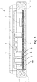
- Fig. 1 shows an embodiment of the optoelectronic miniature sensor 1 in a cross section.
- 2 optical components 3 and electronic components 4 are arranged on one side of a multilayer printed circuit board one side.
- the electronic components 4 are produced on the printed circuit board 2, for example by means of chip-on-board technology (COB).
- COB chip-on-board technology
- other methods are also possible.
- the printed circuit board 2 is particularly thin and consists of at least one conductive copper layer 5, 7, between each of which an insulating layer 6 is formed of a resin and glass fiber fabric.
- a metal plate 8 is arranged, for example, a metal sheet, which is laminated to the lower copper layer 7.
- a further insulating and connecting layer 6a is arranged between the copper layer 7 and the metal plate 8.
- the side of the printed circuit board 2, on which the electronic and optical components 3, 4 are positioned, is covered with a component 9 or cover which is transparent at least in the regions of optical radiation and which covers the electrical radiation from and to the optical components 3 pass through.
- the thus designed optoelectronic miniature sensor 1 is welded to a metal frame 10 circumferentially.
- An optoelectronic miniature sensor 1 with this structure has approximately only half to one third of the height of a conventionally equipped optoelectronic sensor which is stabilized and protected with a housing or cover and at least 1 to 1.2 mm space height for the circuit board together with cover or housing wall required.
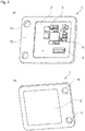
- Fig. 2 is a view of the optoelectronic miniature sensor 1, which is fixed to the metal frame 10.
- Fig. 2a is the top view and in Fig. 2b the underside of the optoelectronic miniature sensor 1 is shown.
- the metal frame 10 has in this case laterally two openings 11, to which the optoelectronic miniature sensor 1, which is arranged uncentered on the metal plate 8, can be mounted at the intended location.
- the metal plate 8 concludes conclusive or optionally slightly tolerance for reasons of tolerance with the metal frame 10 from.
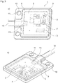
- the optical components 3 and the electronic components 4 are electrically connected via a line 12 to the environment.
- the line 12 is connected to a line end 13 to the circuit board 2.
- This connection point between the line end 13 and the circuit board 2 is also surrounded by the at least partially transparent component 9 or cover.
- the component 9 is designed so that the mounted on the circuit board 2 components 3, 4 and the line end 13 are encapsulated with the cover material, so that a particularly dense coverage of the individual components 3, 4, 13 takes place.
- the proposed solution allows not only a space savings and a better space utilization at the same time a particularly high mechanical stability and robustness of the optoelectronic miniature sensor 1, which can be produced in a few assembly steps and with lower tolerances.
Landscapes
- Engineering & Computer Science (AREA)
- Microelectronics & Electronic Packaging (AREA)
- Manufacturing & Machinery (AREA)
- Physics & Mathematics (AREA)
- General Physics & Mathematics (AREA)
- Light Receiving Elements (AREA)
Abstract
Description
- Die Erfindung betrifft einen optoelektronischer Sensor, vorzugsweise einen optoelektronischen Miniatursensor, umfassend optische und elektronische Bauelemente, welche auf einer einseitig bestückten Leiterplatte positioniert sind.
- Optoelektronische Miniatursensoren erfordern einen besonders platzsparenden Leiterplattenaufbau. Besonders wichtig ist dabei die Leiterplattendicke. Bei kleiner werdender Leiterplattendicke sinkt allerdings die mechanische Stabilität der Leiterplatte, wodurch insbesondere COB (Chip-on-Board)-Elektronikbauteile beschädigt werden können.
- Aus der
DE 10 2005 037 490 A1 ist ein optischer Sensor bekannt, der wenigstens einen Sender, wenigstens einen Empfänger und eine Auswerteeinheit zur Generierung eines Objektfeststellungssignals aufweist. Der Sender und der Empfänger sind dabei auf einer Polymerfolie aufgebracht, die flexibel ausgestaltet ist, wobei die Bereiche mit Sender und Empfänger durch eine Platte versteift werden. Die Bereiche mit dem Sender und dem Empfänger sind jeweils senkrecht zu einem Bereich ausgerichtet, welcher elektronische Bauelemente trägt. - Der Erfindung liegt die Aufgabe zugrunde, einen optoelektronischen Sensor anzugeben, der kostengünstig aufbaubar ist, wobei der Aufbau trotz Verwendung eines platzsparenden Leiterplattenmaterials besonders robust ausgebildet ist. Erfindungsgemäß ist die Aufgabe dadurch gelöst, dass die dünne Leiterplatte mit einer unbestückten Seite auf einer Stabilisierungsplatte unmittelbar aufliegt, wobei die Stabilisierungsplatte eine Außenwandung des Sensors darstellt. Aufgrund der Verwendung dieser Stabilisierungsplatte ist eine robuste Ausgestaltung des optoelektronischen Miniatursensors bei gleichzeitiger Verwendung einer sehr dünnen platzsparenden Leiterplatte möglich. Bauelemente, die nach der Chip-on-Board-Technologie auf der Leiterplatte gefertigt werden, unterliegen einer besonderen Stabilität. Gleichzeitig kann eine elektrische Verbindung über die Stabilisierungsplatte zu weiteren elektronischen Baueinheiten erfolgen.
- Die Stabilisierungsplatte besteht aus Metall. Eine solche Metallplatte erlaubt insbesondere bei der Herstellung von optoelektronischen Miniatursensoren, dass die Dicke der Leiterplatte immer weiter sinken kann und trotzdem eine mechanische Stabilität der Leiterplatte gewährleistet ist.
- Die auf der Leiterplatte angeordneten optischen und elektronischen Bauelemente sind mit einer mindestens teilweise transparenten Komponente abgedeckt. Eine solche teilweise transparente Komponente ermöglicht die Ausstrahlung und den Empfang von Lichtsignalen, wobei die optischen Bauelemente beliebig auf der Leiterplatte verteilt werden können. Es kann sich dabei auch um eine vollständig transparente Komponente bzw. vollständig transparente Abdeckung handeln.
- In einer Ausgestaltung besteht die Stabilisierungsplatte aus einem Edelmetall. Ein solches Edelmetall ist besonders korrosionsfest, weshalb der optoelektronische Sensor mit einer solchen Außenwandung auch in aggressiven Medien eingesetzt werden kann.
- In einer Variante ist die Stabilisierungsplatte an einem Trägerrahmen oder einem Trägergehäuse befestigt. Der so beschaffene optoelektronische Sensor kann als separater Bestandteil mit weiteren Elektronikbauteilen in Verbindung gebracht werden.
- In einer Weiterbildung ist die Stabilisierungsplatte an dem Trägerrahmen oder dem Trägergehäuse umlaufend stoffschlüssig befestigt. Somit lässt sich der optoelektronische Sensor in einem ein Raster bildenden Trägerrahmen oder Trägergehäuse einfach befestigen, wobei die stoffschlüssige Befestigung vorteilhafterweise durch einen Schweißvorgang realisiert wird.
- In einer weiteren Variante ist die teilweise transparente Komponente als Gehäuse ausgebildet. Ein solches Gehäuse stellt eine stabile Abdeckung über den elektronischen und optischen Bauelementen dar, so dass eine mechanische Verletzung der Komponenten unterbunden wird.
- In einer Weiterbildung erfolgt eine elektrische Anbindung der optischen und elektronischen Bauelemente über eine Leitung, welche mit der Leiterplatte verbunden ist, wobei mindestens eine Verbindungsstelle der Leitung mit der Leiterplatte von der teilweise transparenten Abdeckung abgedeckt ist. Somit wird eine Einwirkung von aggressiven Medien auf die Verbindungsstelle durch die transparente Abdeckung unterbunden. Dadurch bleibt die elektrische Verbindung zwischen dem optoelektronischen Sensor und der Umgebung zuverlässig bestehen.
- In einer weiteren Ausführungsform sind die optischen und elektronischen Bauelemente und die Verbindungsstelle der Leitung mit der Leiterplatte durch die teilweise transparente Abdeckung verkapselt. Diese Verkapselung stellt eine besonders dichte Abdeckung dar und verhindert das Eindringen von flüssigen und gasförmigen Medien in die optischen und elektronischen Bauelemente.
- In einer Ausführungsform ist die Leiterplatte als Mehrlagenleiterplatte ausgebildet. Dadurch wird eine platzsparende Kontaktierung mehrerer elektrischer und optischer Bauelemente auf der Leiterplatte ermöglicht.
- In Weiterbildung der Erfindung ist die Stabilisierungsplatte galvanisch, chemisch oder mit anderen Beschichtungsverfahren auf die Leiterplatte aufgetragen.
- Die Erfindung lässt zahlreiche Ausführungsformen zu. Eine davon soll anhand der in der Zeichnung dargestellten Figuren näher erläutert werden.
- Es zeigen:
- Fig. 1
- einen Querschnitt durch den erfindungsgemäßen optoelektronischen Sensor,
- Fig. 2
- eine Draufsicht auf die Vorder- und auf die Unterseite des optoelektronischen Sensors, welcher an einem Trägerrahmen befestigt ist,
- Fig. 3
- ein Ausführungsbeispiel für eine transparente Abdeckung des optoelektronischen Sensors.
-
Fig. 1 zeigt ein Ausführungsbeispiel des optoelektronischen Miniatursensors 1 in einem Querschnitt. Dabei sind auf einer Seite einer mehrlagigen Leiterplatte 2 optische Bauelemente 3 und elektronische Bauelemente 4 einseitig angeordnet. Die elektronischen Bauelemente 4 sind auf der Leiterplatte 2 beispielsweise mittels der chip-on-board-Technologie (COB) hergestellt Es sind jedoch auch andere Verfahren möglich. - Die Leiterplatte 2 ist dabei besonders dünn ausgebildet und besteht aus mindestens einer leitenden Kupferschicht 5, 7, zwischen denen jeweils eine Isolierschicht 6 aus einem Harz und Glasfasergewebe ausgebildet ist. Unter der den optischen und elektrischen Bauteilen 3, 4 abgewandten Kupferschicht 7 ist eine Metallplatte 8 angeordnet, beispielsweise ein Metallblech, welches auf die untere Kupferschicht 7 auflaminiert ist. Alternativ wird zwschen der Kupferschicht 7 und der Metallplatte 8 eine weitere Isolier- und Verbindungsschicht 6a angeordnet. Die Seite der Leiterplatte 2, auf welcher die elektronischen und optischen Bauelemente 3, 4 positioniert sind, ist mit einer mindestens in den Bereichen optischer Strahlung transparenten Komponente 9 bzw. Abdeckung abgedeckt, welche die elektrische Strahlung von und zu den optischen Bauelementen 3 durchlässt. Der so ausgestaltete optoelektro-nische Miniatursensor 1 ist an einem Metallrahmen 10 umlaufend angeschweißt.
- Ein optoelektronischer Miniatursensor 1 mit diesem Aufbau weist etwa nur die Hälfte bis ein Drittel der Höhe eines konventionell bestückten optoelektronischen Sensors auf, welcher mit einem Gehäuse oder Deckel stabilisiert und geschützt ist und mindestens 1 bis 1,2 mm Bauraumhöhe für die Leiterplatte zusammen mit Deckel- bzw. Gehäusewandung benötigt.
- In
Fig. 2 ist eine Ansicht auf den optoelektronischen Miniatursensor 1 dargestellt, welcher an dem Metallrahmen 10 befestigt ist. InFig. 2a ist die Draufsicht und inFig. 2b die Unterseite des optoelektronischen Miniatursensors 1 gezeigt. Der Metallrahmen 10 weist dabei seitlich zwei Öffnungen 11 auf, an welchen der optoelektronische Miniatursensor 1, der unzentriert auf der Metallplatte 8 angeordnet ist, an dem vorgesehenen Einsatzort montiert werden kann. Auf der Unterseite schließt die Metallplatte 8 schlüssig oder optional aus Toleranzgründen leicht vertieft mit dem Metallrahmen 10 ab. - Wie in
Fig. 3a und 3b dargestellt, sind die optischen Bauelemente 3 und die elektronischen Bauelemente 4 über eine Leitung 12 mit der Umgebung elektrisch verbunden. Zu diesem Zweck ist die Leitung 12 mit einem Leitungsende 13 mit der Leiterplatte 2 verbunden. Diese Verbindungsstelle zwischen dem Leitungsende 13 und der Leiterplatte 2 ist ebenfalls von der mindestens teilweise transparenten Komponente 9 bzw. Abdeckung umgeben. Die Komponente 9 ist dabei so ausgebildet, dass die auf der Leiterplatte 2 befestigten Bauelemente 3, 4 und das Leitungsende 13 mit dem Abdeckungsmaterial verkapselt sind, so dass eine besonders dichte Abdeckung der einzelnen Bauteile 3, 4, 13 erfolgt. - Die vorgeschlagene Lösung erlaubt neben einer Platzersparnis und einer besseren Bauraumausnutzung gleichzeitig eine besonders hohe mechanische Stabilität und Robustheit des optoelektronischen Miniatursensors 1, welcher in wenigen Montageschritten und bei geringeren Toleranzen herstellbar ist.
Claims (9)
- Optoelektronischer Sensor, vorzugsweise ein optoelektronischer Miniatursensor, umfassend optische und elektronische Bauelemente (3, 4), welche auf einer einseitig bestückten Leiterplatte (2) positioniert sind, dadurch gekennzeichnet, dass die dünne Leiterplatte (2) mit einer unbestückten Seite auf einer Stabilisierungsplatte (8) unmittelbar aufliegt, wobei die Stabilisierungsplatte (8) eine Außenwandung des Sensors (1) bildet, dadurch gekennzeichnet, dass die Stabilisierungsplatte (8) aus Metall besteht, wobei die auf der Leiterplatte (2) angeordneten optischen und elektronischen Bauelemente (3, 4) mit einer mindestens teilweise transparenten Komponente (9) abgedeckt sind.
- Optoelektronischer Sensor nach Anspruch 1, dadurch gekennzeichnet, dass die Stabilisierungsplatte (8) aus einem Edelmetall besteht.
- Optoelektronischer Sensor nach Anspruch 1 oder 2, dadurch gekennzeichnet, dass die Stabilisierungsplatte (8) an einem Trägerrahmen (10) oder einem Trägergehäuse befestigt ist.
- Optoelektronischer Sensor nach Anspruch 3, dadurch gekennzeichnet, dass die Stabilisierungsplatte (8) an dem Trägerrahmen (10) oder dem Trägergehäuse umlaufend stoffschlüssig befestigt ist.
- Optoelektronischer Sensor nach Anspruch 1, dadurch gekennzeichnet, dass die Komponente (9) als Gehäuse ausgebildet ist.
- Optoelektronischer Sensor nach mindestens einem der vorhergehenden Ansprüche, dadurch gekennzeichnet, dass eine elektrische Anbindung der optischen und elektronischen Bauelemente (3, 4) mit einer Leitung (12) erfolgt, welche mit der Leiterplatte (2) verbunden ist, wobei mindestens eine Verbindungsstelle (13) der Leitung (12) mit der Leitungsplatte (2) von der Komponente (9) abgedeckt ist.
- Optoelektronischer Sensor nach Anspruch 1 oder 6, dadurch gekennzeichnet, dass die optischen und elektronischen Bauelemente (3, 4) und/oder die Verbindungsstelle (13) der Leitung (12) mit der Leiterplatte (2) durch die Komponente (9) verkapselt sind.
- Optoelektronischer Sensor nach mindestens einem der vorhergehenden Ansprüche, dadurch gekennzeichnet, dass die Leiterplatte (2) als Mehrlagenleiterplatte ausgebildet ist.
- Optoelektronischer Sensor nach mindestens einem der vorhergehenden Ansprüche, dadurch gekennzeichnet, dass die Stabilisierungsplatte (8) galvanisch, chemisch oder mit anderen Beschichtungsverfahren auf die Leiterplatte (2) aufgetragen ist.
Applications Claiming Priority (1)
| Application Number | Priority Date | Filing Date | Title |
|---|---|---|---|
| DE102017123553.1A DE102017123553A1 (de) | 2017-10-10 | 2017-10-10 | Optoelektronischer Sensor |
Publications (2)
| Publication Number | Publication Date |
|---|---|
| EP3470797A1 true EP3470797A1 (de) | 2019-04-17 |
| EP3470797B1 EP3470797B1 (de) | 2020-03-25 |
Family
ID=63371503
Family Applications (1)
| Application Number | Title | Priority Date | Filing Date |
|---|---|---|---|
| EP18190293.3A Active EP3470797B1 (de) | 2017-10-10 | 2018-08-22 | Optoelektronischer sensor |
Country Status (2)
| Country | Link |
|---|---|
| EP (1) | EP3470797B1 (de) |
| DE (1) | DE102017123553A1 (de) |
Citations (4)
| Publication number | Priority date | Publication date | Assignee | Title |
|---|---|---|---|---|
| DE19842881A1 (de) * | 1997-09-22 | 1999-03-25 | Fuji Electric Co Ltd | Halbleiter-Optosensor |
| US20040080642A1 (en) * | 2002-09-27 | 2004-04-29 | Kenichi Kobayashi | Camera module |
| DE102005032453A1 (de) * | 2005-07-12 | 2007-01-25 | Robert Bosch Gmbh | Optoelektronische Vorrichtung, insbesondere optischer Sensor, Sensoranordnung und Verfahren |
| DE102015208486A1 (de) * | 2015-05-07 | 2016-11-10 | Conti Temic Microelectronic Gmbh | Elektronische Komponente und Verfahren zu deren Herstellung |
Family Cites Families (6)
| Publication number | Priority date | Publication date | Assignee | Title |
|---|---|---|---|---|
| EP0690692A4 (de) * | 1992-12-01 | 1999-02-10 | Somanetics Corp | Fühler für optische oximetrie am grosshirn eines patienten |
| DE102004021931A1 (de) * | 2004-03-16 | 2005-10-06 | Robert Bosch Gmbh | Gehäuse für eine elektronische Schaltung |
| DE102005014671A1 (de) * | 2005-03-29 | 2006-10-05 | Hella Kgaa Hueck & Co. | Innenleuchte für Fahrzeuge |
| DE102005037490A1 (de) | 2005-08-09 | 2007-02-15 | Leuze Electronic Gmbh & Co Kg | Optischer Sensor |
| KR20130022751A (ko) * | 2011-08-26 | 2013-03-07 | (주) 파루 | 태양광 추적센서 및 이를 이용한 태양광 집광장치 |
| US10653332B2 (en) * | 2015-07-17 | 2020-05-19 | Mc10, Inc. | Conductive stiffener, method of making a conductive stiffener, and conductive adhesive and encapsulation layers |
-
2017
- 2017-10-10 DE DE102017123553.1A patent/DE102017123553A1/de not_active Withdrawn
-
2018
- 2018-08-22 EP EP18190293.3A patent/EP3470797B1/de active Active
Patent Citations (4)
| Publication number | Priority date | Publication date | Assignee | Title |
|---|---|---|---|---|
| DE19842881A1 (de) * | 1997-09-22 | 1999-03-25 | Fuji Electric Co Ltd | Halbleiter-Optosensor |
| US20040080642A1 (en) * | 2002-09-27 | 2004-04-29 | Kenichi Kobayashi | Camera module |
| DE102005032453A1 (de) * | 2005-07-12 | 2007-01-25 | Robert Bosch Gmbh | Optoelektronische Vorrichtung, insbesondere optischer Sensor, Sensoranordnung und Verfahren |
| DE102015208486A1 (de) * | 2015-05-07 | 2016-11-10 | Conti Temic Microelectronic Gmbh | Elektronische Komponente und Verfahren zu deren Herstellung |
Also Published As
| Publication number | Publication date |
|---|---|
| EP3470797B1 (de) | 2020-03-25 |
| DE102017123553A1 (de) | 2019-04-11 |
Similar Documents
| Publication | Publication Date | Title |
|---|---|---|
| DE202007018944U1 (de) | Winkelsensor | |
| DE102014014050B4 (de) | Näherungssensoranordnung | |
| EP1367879A2 (de) | Elektrische Vorrichtung | |
| DE19820414A1 (de) | Kontaktierungsvorrichtung | |
| DE102018205014A1 (de) | Antenneneinheit | |
| DE102010010331A1 (de) | Elektrische Kontaktanordnung | |
| EP2036414B1 (de) | Befestigungseinrichtung und verfahren zur befestigung einer leiterplatte in einem gehäuse | |
| WO2016177496A1 (de) | Elektrische verbindungsanordnung | |
| DE202017106142U1 (de) | Optoelektronischer Sensor | |
| EP4054377B1 (de) | Bauelement zur elektrischen kontaktierung wenigstens eines funktionselements an einem textil o.ä. und anordnung mit einem bauelement | |
| WO1998025443A1 (de) | Elektronischer schaltkreis mit einem hockfrequenzbedämpfenden schirmgehäuse | |
| DE102014217923A1 (de) | Leiterplattenanordnung, insbesondere für Kfz-Getriebesteuergerät, mit zwei miteinander verbundenen Leiterplatten und einem Spanschutz | |
| DE202012002352U1 (de) | Anordnung aus Steckverbinder und Leiterplatte | |
| DE10307674A1 (de) | Induktiver Sensor und damit ausgestatteter Drehgeber | |
| EP3470797B1 (de) | Optoelektronischer sensor | |
| DE102018105501B4 (de) | Abschirmvorrichtung für eine Ultraschallsensorvorrichtung und Verfahren zur Herstellung einer Ultraschallsensorvorrichtung | |
| DE202015008007U1 (de) | Leiterplattenanordnung | |
| DE102016123437A1 (de) | Radarsensor für ein Fahrzeug und Verfahren zum Zusammenbau eines Radarsensors | |
| EP3355075A1 (de) | Sensoranordnung | |
| DE602006000047T2 (de) | Planare Antennenanordnung | |
| DE102010029868A1 (de) | Getriebesteuerung | |
| DE102007017707B3 (de) | Leiterplatten-Schirmblech-Anordnung | |
| EP4242596B1 (de) | Sensoreinheit | |
| DE102019203825A1 (de) | Winkelerfassungseinrichtung | |
| WO2020188053A1 (de) | Winkelerfassungseinrichtung |
Legal Events
| Date | Code | Title | Description |
|---|---|---|---|
| PUAI | Public reference made under article 153(3) epc to a published international application that has entered the european phase |
Free format text: ORIGINAL CODE: 0009012 |
|
| STAA | Information on the status of an ep patent application or granted ep patent |
Free format text: STATUS: THE APPLICATION HAS BEEN PUBLISHED |
|
| AK | Designated contracting states |
Kind code of ref document: A1 Designated state(s): AL AT BE BG CH CY CZ DE DK EE ES FI FR GB GR HR HU IE IS IT LI LT LU LV MC MK MT NL NO PL PT RO RS SE SI SK SM TR |
|
| AX | Request for extension of the european patent |
Extension state: BA ME |
|
| STAA | Information on the status of an ep patent application or granted ep patent |
Free format text: STATUS: REQUEST FOR EXAMINATION WAS MADE |
|
| 17P | Request for examination filed |
Effective date: 20190911 |
|
| RBV | Designated contracting states (corrected) |
Designated state(s): AL AT BE BG CH CY CZ DE DK EE ES FI FR GB GR HR HU IE IS IT LI LT LU LV MC MK MT NL NO PL PT RO RS SE SI SK SM TR |
|
| GRAP | Despatch of communication of intention to grant a patent |
Free format text: ORIGINAL CODE: EPIDOSNIGR1 |
|
| STAA | Information on the status of an ep patent application or granted ep patent |
Free format text: STATUS: GRANT OF PATENT IS INTENDED |
|
| INTG | Intention to grant announced |
Effective date: 20200103 |
|
| GRAS | Grant fee paid |
Free format text: ORIGINAL CODE: EPIDOSNIGR3 |
|
| RAP1 | Party data changed (applicant data changed or rights of an application transferred) |
Owner name: SICK AG |
|
| GRAA | (expected) grant |
Free format text: ORIGINAL CODE: 0009210 |
|
| STAA | Information on the status of an ep patent application or granted ep patent |
Free format text: STATUS: THE PATENT HAS BEEN GRANTED |
|
| AK | Designated contracting states |
Kind code of ref document: B1 Designated state(s): AL AT BE BG CH CY CZ DE DK EE ES FI FR GB GR HR HU IE IS IT LI LT LU LV MC MK MT NL NO PL PT RO RS SE SI SK SM TR |
|
| REG | Reference to a national code |
Ref country code: GB Ref legal event code: FG4D Free format text: NOT ENGLISH |
|
| REG | Reference to a national code |
Ref country code: DE Ref legal event code: R096 Ref document number: 502018001030 Country of ref document: DE |
|
| REG | Reference to a national code |
Ref country code: AT Ref legal event code: REF Ref document number: 1249082 Country of ref document: AT Kind code of ref document: T Effective date: 20200415 Ref country code: IE Ref legal event code: FG4D Free format text: LANGUAGE OF EP DOCUMENT: GERMAN |
|
| PG25 | Lapsed in a contracting state [announced via postgrant information from national office to epo] |
Ref country code: FI Free format text: LAPSE BECAUSE OF FAILURE TO SUBMIT A TRANSLATION OF THE DESCRIPTION OR TO PAY THE FEE WITHIN THE PRESCRIBED TIME-LIMIT Effective date: 20200325 Ref country code: RS Free format text: LAPSE BECAUSE OF FAILURE TO SUBMIT A TRANSLATION OF THE DESCRIPTION OR TO PAY THE FEE WITHIN THE PRESCRIBED TIME-LIMIT Effective date: 20200325 Ref country code: NO Free format text: LAPSE BECAUSE OF FAILURE TO SUBMIT A TRANSLATION OF THE DESCRIPTION OR TO PAY THE FEE WITHIN THE PRESCRIBED TIME-LIMIT Effective date: 20200625 |
|
| PG25 | Lapsed in a contracting state [announced via postgrant information from national office to epo] |
Ref country code: BG Free format text: LAPSE BECAUSE OF FAILURE TO SUBMIT A TRANSLATION OF THE DESCRIPTION OR TO PAY THE FEE WITHIN THE PRESCRIBED TIME-LIMIT Effective date: 20200625 Ref country code: LV Free format text: LAPSE BECAUSE OF FAILURE TO SUBMIT A TRANSLATION OF THE DESCRIPTION OR TO PAY THE FEE WITHIN THE PRESCRIBED TIME-LIMIT Effective date: 20200325 Ref country code: SE Free format text: LAPSE BECAUSE OF FAILURE TO SUBMIT A TRANSLATION OF THE DESCRIPTION OR TO PAY THE FEE WITHIN THE PRESCRIBED TIME-LIMIT Effective date: 20200325 Ref country code: GR Free format text: LAPSE BECAUSE OF FAILURE TO SUBMIT A TRANSLATION OF THE DESCRIPTION OR TO PAY THE FEE WITHIN THE PRESCRIBED TIME-LIMIT Effective date: 20200626 Ref country code: HR Free format text: LAPSE BECAUSE OF FAILURE TO SUBMIT A TRANSLATION OF THE DESCRIPTION OR TO PAY THE FEE WITHIN THE PRESCRIBED TIME-LIMIT Effective date: 20200325 |
|
| REG | Reference to a national code |
Ref country code: NL Ref legal event code: MP Effective date: 20200325 |
|
| REG | Reference to a national code |
Ref country code: LT Ref legal event code: MG4D |
|
| PG25 | Lapsed in a contracting state [announced via postgrant information from national office to epo] |
Ref country code: NL Free format text: LAPSE BECAUSE OF FAILURE TO SUBMIT A TRANSLATION OF THE DESCRIPTION OR TO PAY THE FEE WITHIN THE PRESCRIBED TIME-LIMIT Effective date: 20200325 |
|
| PG25 | Lapsed in a contracting state [announced via postgrant information from national office to epo] |
Ref country code: PT Free format text: LAPSE BECAUSE OF FAILURE TO SUBMIT A TRANSLATION OF THE DESCRIPTION OR TO PAY THE FEE WITHIN THE PRESCRIBED TIME-LIMIT Effective date: 20200818 Ref country code: IS Free format text: LAPSE BECAUSE OF FAILURE TO SUBMIT A TRANSLATION OF THE DESCRIPTION OR TO PAY THE FEE WITHIN THE PRESCRIBED TIME-LIMIT Effective date: 20200725 Ref country code: SK Free format text: LAPSE BECAUSE OF FAILURE TO SUBMIT A TRANSLATION OF THE DESCRIPTION OR TO PAY THE FEE WITHIN THE PRESCRIBED TIME-LIMIT Effective date: 20200325 Ref country code: SM Free format text: LAPSE BECAUSE OF FAILURE TO SUBMIT A TRANSLATION OF THE DESCRIPTION OR TO PAY THE FEE WITHIN THE PRESCRIBED TIME-LIMIT Effective date: 20200325 Ref country code: EE Free format text: LAPSE BECAUSE OF FAILURE TO SUBMIT A TRANSLATION OF THE DESCRIPTION OR TO PAY THE FEE WITHIN THE PRESCRIBED TIME-LIMIT Effective date: 20200325 Ref country code: LT Free format text: LAPSE BECAUSE OF FAILURE TO SUBMIT A TRANSLATION OF THE DESCRIPTION OR TO PAY THE FEE WITHIN THE PRESCRIBED TIME-LIMIT Effective date: 20200325 Ref country code: CZ Free format text: LAPSE BECAUSE OF FAILURE TO SUBMIT A TRANSLATION OF THE DESCRIPTION OR TO PAY THE FEE WITHIN THE PRESCRIBED TIME-LIMIT Effective date: 20200325 Ref country code: RO Free format text: LAPSE BECAUSE OF FAILURE TO SUBMIT A TRANSLATION OF THE DESCRIPTION OR TO PAY THE FEE WITHIN THE PRESCRIBED TIME-LIMIT Effective date: 20200325 |
|
| REG | Reference to a national code |
Ref country code: DE Ref legal event code: R097 Ref document number: 502018001030 Country of ref document: DE |
|
| PG25 | Lapsed in a contracting state [announced via postgrant information from national office to epo] |
Ref country code: DK Free format text: LAPSE BECAUSE OF FAILURE TO SUBMIT A TRANSLATION OF THE DESCRIPTION OR TO PAY THE FEE WITHIN THE PRESCRIBED TIME-LIMIT Effective date: 20200325 Ref country code: ES Free format text: LAPSE BECAUSE OF FAILURE TO SUBMIT A TRANSLATION OF THE DESCRIPTION OR TO PAY THE FEE WITHIN THE PRESCRIBED TIME-LIMIT Effective date: 20200325 |
|
| PLBE | No opposition filed within time limit |
Free format text: ORIGINAL CODE: 0009261 |
|
| STAA | Information on the status of an ep patent application or granted ep patent |
Free format text: STATUS: NO OPPOSITION FILED WITHIN TIME LIMIT |
|
| PG25 | Lapsed in a contracting state [announced via postgrant information from national office to epo] |
Ref country code: PL Free format text: LAPSE BECAUSE OF FAILURE TO SUBMIT A TRANSLATION OF THE DESCRIPTION OR TO PAY THE FEE WITHIN THE PRESCRIBED TIME-LIMIT Effective date: 20200325 |
|
| 26N | No opposition filed |
Effective date: 20210112 |
|
| PG25 | Lapsed in a contracting state [announced via postgrant information from national office to epo] |
Ref country code: MC Free format text: LAPSE BECAUSE OF FAILURE TO SUBMIT A TRANSLATION OF THE DESCRIPTION OR TO PAY THE FEE WITHIN THE PRESCRIBED TIME-LIMIT Effective date: 20200325 |
|
| PG25 | Lapsed in a contracting state [announced via postgrant information from national office to epo] |
Ref country code: LU Free format text: LAPSE BECAUSE OF NON-PAYMENT OF DUE FEES Effective date: 20200822 |
|
| REG | Reference to a national code |
Ref country code: BE Ref legal event code: MM Effective date: 20200831 |
|
| PG25 | Lapsed in a contracting state [announced via postgrant information from national office to epo] |
Ref country code: SI Free format text: LAPSE BECAUSE OF FAILURE TO SUBMIT A TRANSLATION OF THE DESCRIPTION OR TO PAY THE FEE WITHIN THE PRESCRIBED TIME-LIMIT Effective date: 20200325 |
|
| PG25 | Lapsed in a contracting state [announced via postgrant information from national office to epo] |
Ref country code: BE Free format text: LAPSE BECAUSE OF NON-PAYMENT OF DUE FEES Effective date: 20200831 Ref country code: IE Free format text: LAPSE BECAUSE OF NON-PAYMENT OF DUE FEES Effective date: 20200822 |
|
| REG | Reference to a national code |
Ref country code: CH Ref legal event code: PL |
|
| PG25 | Lapsed in a contracting state [announced via postgrant information from national office to epo] |
Ref country code: LI Free format text: LAPSE BECAUSE OF NON-PAYMENT OF DUE FEES Effective date: 20210831 Ref country code: CH Free format text: LAPSE BECAUSE OF NON-PAYMENT OF DUE FEES Effective date: 20210831 |
|
| PG25 | Lapsed in a contracting state [announced via postgrant information from national office to epo] |
Ref country code: TR Free format text: LAPSE BECAUSE OF FAILURE TO SUBMIT A TRANSLATION OF THE DESCRIPTION OR TO PAY THE FEE WITHIN THE PRESCRIBED TIME-LIMIT Effective date: 20200325 Ref country code: MT Free format text: LAPSE BECAUSE OF FAILURE TO SUBMIT A TRANSLATION OF THE DESCRIPTION OR TO PAY THE FEE WITHIN THE PRESCRIBED TIME-LIMIT Effective date: 20200325 Ref country code: CY Free format text: LAPSE BECAUSE OF FAILURE TO SUBMIT A TRANSLATION OF THE DESCRIPTION OR TO PAY THE FEE WITHIN THE PRESCRIBED TIME-LIMIT Effective date: 20200325 |
|
| PG25 | Lapsed in a contracting state [announced via postgrant information from national office to epo] |
Ref country code: MK Free format text: LAPSE BECAUSE OF FAILURE TO SUBMIT A TRANSLATION OF THE DESCRIPTION OR TO PAY THE FEE WITHIN THE PRESCRIBED TIME-LIMIT Effective date: 20200325 Ref country code: AL Free format text: LAPSE BECAUSE OF FAILURE TO SUBMIT A TRANSLATION OF THE DESCRIPTION OR TO PAY THE FEE WITHIN THE PRESCRIBED TIME-LIMIT Effective date: 20200325 |
|
| GBPC | Gb: european patent ceased through non-payment of renewal fee |
Effective date: 20220822 |
|
| PG25 | Lapsed in a contracting state [announced via postgrant information from national office to epo] |
Ref country code: GB Free format text: LAPSE BECAUSE OF NON-PAYMENT OF DUE FEES Effective date: 20220822 |
|
| PGFP | Annual fee paid to national office [announced via postgrant information from national office to epo] |
Ref country code: DE Payment date: 20250819 Year of fee payment: 8 |
|
| PGFP | Annual fee paid to national office [announced via postgrant information from national office to epo] |
Ref country code: IT Payment date: 20250829 Year of fee payment: 8 |
|
| PGFP | Annual fee paid to national office [announced via postgrant information from national office to epo] |
Ref country code: AT Payment date: 20250819 Year of fee payment: 8 Ref country code: FR Payment date: 20250821 Year of fee payment: 8 |