EP3465232B1 - Messvorrichtung zur messung von parametern elektrischer grösse - Google Patents
Messvorrichtung zur messung von parametern elektrischer grösse Download PDFInfo
- Publication number
- EP3465232B1 EP3465232B1 EP16731809.6A EP16731809A EP3465232B1 EP 3465232 B1 EP3465232 B1 EP 3465232B1 EP 16731809 A EP16731809 A EP 16731809A EP 3465232 B1 EP3465232 B1 EP 3465232B1
- Authority
- EP
- European Patent Office
- Prior art keywords
- voltage
- capacitive
- measure
- current
- signal
- Prior art date
- Legal status (The legal status is an assumption and is not a legal conclusion. Google has not performed a legal analysis and makes no representation as to the accuracy of the status listed.)
- Active
Links
Images


Classifications
-
- G—PHYSICS
- G01—MEASURING; TESTING
- G01R—MEASURING ELECTRIC VARIABLES; MEASURING MAGNETIC VARIABLES
- G01R15/00—Details of measuring arrangements of the types provided for in groups G01R17/00 - G01R29/00, G01R33/00 - G01R33/26 or G01R35/00
- G01R15/12—Circuits for multi-testers, i.e. multimeters, e.g. for measuring voltage, current, or impedance at will
-
- G—PHYSICS
- G01—MEASURING; TESTING
- G01R—MEASURING ELECTRIC VARIABLES; MEASURING MAGNETIC VARIABLES
- G01R15/00—Details of measuring arrangements of the types provided for in groups G01R17/00 - G01R29/00, G01R33/00 - G01R33/26 or G01R35/00
- G01R15/14—Adaptations providing voltage or current isolation, e.g. for high-voltage or high-current networks
- G01R15/16—Adaptations providing voltage or current isolation, e.g. for high-voltage or high-current networks using capacitive devices
-
- G—PHYSICS
- G01—MEASURING; TESTING
- G01R—MEASURING ELECTRIC VARIABLES; MEASURING MAGNETIC VARIABLES
- G01R15/00—Details of measuring arrangements of the types provided for in groups G01R17/00 - G01R29/00, G01R33/00 - G01R33/26 or G01R35/00
- G01R15/14—Adaptations providing voltage or current isolation, e.g. for high-voltage or high-current networks
- G01R15/18—Adaptations providing voltage or current isolation, e.g. for high-voltage or high-current networks using inductive devices, e.g. transformers
-
- G—PHYSICS
- G01—MEASURING; TESTING
- G01R—MEASURING ELECTRIC VARIABLES; MEASURING MAGNETIC VARIABLES
- G01R21/00—Arrangements for measuring electric power or power factor
- G01R21/006—Measuring power factor
-
- G—PHYSICS
- G01—MEASURING; TESTING
- G01R—MEASURING ELECTRIC VARIABLES; MEASURING MAGNETIC VARIABLES
- G01R25/00—Arrangements for measuring phase angle between a voltage and a current or between voltages or currents
-
- G—PHYSICS
- G01—MEASURING; TESTING
- G01R—MEASURING ELECTRIC VARIABLES; MEASURING MAGNETIC VARIABLES
- G01R27/00—Arrangements for measuring resistance, reactance, impedance, or electric characteristics derived therefrom
- G01R27/02—Measuring real or complex resistance, reactance, impedance, or other two-pole characteristics derived therefrom, e.g. time constant
- G01R27/26—Measuring inductance or capacitance; Measuring quality factor, e.g. by using the resonance method; Measuring loss factor; Measuring dielectric constants ; Measuring impedance or related variables
- G01R27/2605—Measuring capacitance
Definitions
- the present invention generally relates to a meter apparatus for measuring parameters (e.g., amplitude and/or phase shift) of electrical quantities (e.g., electric voltage and/or electric current).
- the present invention relates to a meter apparatus for effectively measuring parameters of electrical quantities of any wire in operation without the use of batteries and in a non-intrusive manner.
- determining the amplitude of the electric voltage and of the electric current in line and neutral wires in an electrical distribution system permits to determine harmonic distortion in that electrical distribution system.
- Harmonic distortion typically affects electric loads (such as personal computers, laser printers, battery chargers, and other small appliances) powered by "Switched-Mode Power Supply” (SMPS) modules, and may cause, inter alia, large load currents in the neutral wire of a three-phase electrical distribution system (which can cause potential fire hazards, as only the line wire is usually protected by circuit breakers), overheating (which may shorten the life of the electronic devices), poor power factor of the electric loads (e.g. power factor lower than 0.9, which could result in monthly utility penalty fees), resonance (which produces over-current surges), false tripping of circuit breakers, and electric load malfunctions.
- SMPS Switchched-Mode Power Supply
- a meter apparatus based on single-sensor approach allows monitoring an electrical circuit that contains a number of electric loads which switch on and off independently, and makes use of an on-site analysis of the electric current and electric voltage waveforms for estimating the number of electric loads, the nature of each electric load, the energy consumption of each electric load, and other relevant statistics such as time-of-day variations.
- meter apparatuses based on single-sensor approach are easier to deploy, they nevertheless rely on expensive custom hardware, and require either a priori knowledge about the electric loads and their electrical characteristics or a complex training phase involving the user (where the apparatus learns about the specific electrical characteristics of the electric loads).
- A-priori knowledge is difficult to obtain, and to keep updated, in a modern context of fast changing small appliances, and training procedures discourage users.
- a meter apparatus based on multi-sensor approach comprises a current sensor installed in-line with each load (such as a commercially available smart power outlet) for measuring the power consumption at the point where the electric load is placed, or measure point, and a central gateway for gathering (and possibly displaying) the measured power consumption from each electric load.
- each load such as a commercially available smart power outlet
- a central gateway for gathering (and possibly displaying) the measured power consumption from each electric load.
- the meter apparatus design shown in this document operates automatically and is considered with installation difficulties and environmental effects such as position displacement due to weather, electrical and magnetic field interaction and so on.
- Each meter apparatus collects current, voltage and associated phase angles and proceed to carry a two-way communication to form a sensors net using which a RF commercial communication module.
- US6825649 discloses a measurement method for measuring an AC voltage applied to a conductor, without contacting the conductor, using a detection probe, provided with a detection electrode capable of covering part of a surface of insulation for insulating the conductor and a shield electrode for covering the detection electrode, and an oscillator for outputting a signal having a certain frequency, wherein one end of each of a core wire and a sheath wire of a shield cable are connected to the detection electrode and the shield electrode, and a floating capacitance effect is substantially made zero by establishing an imaginary short-circuit state between each of the other ends.
- the measurement method comprises the steps of measuring impedance between the detection electrode and the conductor by applying the signal from an oscillator to the detection electrode via the shield cable, measuring a current discharged from the detection electrode attributable to the voltage applied to the conductor, and obtaining the applied voltage based on the measured impedance and current.
- US2010/318306 discloses an apparatus for monitoring the voltage of electricity supplied on a cable.
- the apparatus includes a sense electrode housed in an electrically-insulative housing to form a capacitive coupling between the sense electrode and the cable.
- the housing may be of the clamp-on type.
- a sense capacitor of known capacitance is included, which is electrically coupled to the sense electrode and a local ground.
- Suitable voltage measurement circuitry is connected to the sense capacitor and is responsive to voltage produced across the sense capacitor to provide an output signal representative of the voltage on the cable.
- the measured voltage waveform can be filtered to give the fundamental of the supply voltage, which can eliminate or reduce the effects of changes in capacitance within one cycle.
- a secondary capacitive coupling can be formed with a related neutral wire to improve stability of the voltage waveform measurement.
- US 5 473 244 discloses an apparatus for performing non-contacting measurements of the voltage, current and power levels of conductive elements such as wires, cables and the like, which includes an arrangement of capacitive sensors for generating a first current in response to variation in voltage of a conductive element. Each sensor is positioned in an electric field of the conductive element, and is thereby coupled to the conductive element through a coupling capacitance.
- a reference source drives the capacitive sensor arrangement at a reference frequency so as to induce the flow of a reference current therethrough.
- a measurement network is disposed to calculate the coupling capacitance based on a measurement of the reference current, and to then determine the voltage in the conductive element based on the first current and the coupling capacitance.
- Measurements of a composite current through single or multiple-element conductors may be effected using a similar procedure, wherein the composite current induces a measurement current to flow within a set of coils positioned in a predetermined manner proximate the conductor.
- a balancing procedure may be employed, in which a measurement signal is balanced by a feedback signal so as to improve accuracy and reduce the effects of stray coupling.
- each meter apparatus is arranged for collecting current, voltage and associated phase angles in an intrusive manner, which makes measurements not fully reliable.
- this paper does not face any issue that affects real measurements, such as wire geometry (which may also significantly differ from a measure point to another one) and wire spatial geometry or arrangement (indeed, a wire at a measure point cannot be approximated as a rectilinear conductor if, for example, it is bent).
- US6825649 only discloses a voltage monitoring, without taking into account parameters relating to phase shift (such as Power Factor). Moreover, the Applicant has understood that US6825649 , similarly to the " Self-powered smart meter with synchronized data" paper, does not face any issue that affects real measurements, such as wire geometry and wire spatial geometry or arrangement.
- the Applicant has faced the issue of determining the electric voltage and/or electric current waveforms (or relevant parameters thereof) of an AC signal in a non-intrusive manner, and independently from wire geometry and from wire spatial geometry or arrangement at the measure point, and, in order to achieve that, has devised a low cost and effective meter apparatus (and method) addressing this issue.
- an aspect of the present invention relates to a meter apparatus for determining parameters of an AC electric signal in first and second wires, the AC electric signal comprising an AC electric current and an AC electric voltage.
- the meter apparatus comprises:
- the meter apparatus further comprises a further measurement section configured for providing a third measure signal indicative of the AC electric current based on an inductive coupling with the first or second wire.
- the control unit is further configured for: determining a phase shift between the AC electric voltage and the AC electric current according to a phase shift between the first and third measure signals.
- the meter apparatus further comprises first and second capacitive elements for performing said first and second capacitive couplings.
- Said first and second capacitive elements preferably comprise at least a portion of said first and second wires.
- said measurement section further comprises first and second input capacitive elements electrically coupleable to the first and second capacitive elements, respectively.
- the first and second capacitive elements and, respectively, the first and second input capacitive elements define, when coupled to each other, an impedance voltage divider for providing said first measure signal from said AC electric voltage, the first measure signal being in phase with respect to said AC electric voltage.
- said measurement section comprises further first and further second capacitive elements electrically coupleable to the first and second capacitive elements, respectively.
- the first and second capacitive elements and, respectively, the further first and further second capacitive elements preferably define, when coupled to each other, an impedance voltage divider providing said second measure signal from said AC electric voltage, the first and second measure signals being in phase with respect to each other.
- said measurement section comprises first and second circuit arrangements electrically coupleable to the first and second capacitive elements, respectively.
- the first and second capacitive elements and, respectively, the first and second circuit arrangements preferably define, when coupled to each other, a differentiator arrangement providing said second measure signal from said AC electric voltage.
- control unit is arranged for determining said capacitance values of the first and second capacitive couplings according to amplitudes of the first and second measure signals.
- control unit is further arranged for determining the amplitude of the AC electric voltage according to the amplitudes of first or second measure signal and to the capacitance values of the first and second capacitive couplings.
- the first and second measure signals have a phase shift with respect to each other, said phase shift between the first and second measure signals depending on the capacitance values of the first and second capacitive couplings.
- the control unit is further arranged for:
- said measurement section comprises first and second resistive elements electrically coupleable to the first and second capacitive elements, respectively.
- the first and second capacitive elements and, respectively, the first and second resistive elements define, when coupled to each other, a high-pass filter providing said second measure signal from said AC electric voltage.
- the further measurement section comprises an energy harvesting module for harvesting energy from said inductive coupling.
- the further measurement section also comprises a switching device selectively operable in a first configuration allowing energy harvesting by said energy harvesting unit or in a second configuration allowing provision of the third measure signal and preventing said energy harvesting.
- the further measurement section further comprises a charge storage element for storing electric charge according to said energy harvesting and for supplying said electric charge to the measurement section, to the further measurement section, and to the control unit.
- the further measurement section comprises a current clamp device for performing said inductive coupling with the first or second wires.
- the current clamp device comprises a split core current transformer.
- said measurement section comprises first and second electrically conductive layers adapted to be provided on portions of the first and second wires, respectively.
- the portion of the first wire and the first electrically conductive layer thereon define said first capacitive element between the first wire and the measurement section, and, preferably, the portion of the second wire and the second electrically conductive layer thereon define said second capacitive element between the second wire and the measurement section.
- Another aspect of the present invention relates to a corresponding method for determining said parameters of the AC electric signal.
- the present invention allows determining electric voltage and/or electric current waveforms (i.e., amplitude and phase shift) of an AC signal (for example, the AC signal in the line and neutral wires of an electrical distribution system) by using inductive and capacitive couplings. Thanks to inductive and capacitive couplings, the electric voltage and/or electric current waveforms are determined in a non-intrusive manner (i.e., without altering the overall load of the electrical distribution system) and independently from wire geometry (which may also significantly differ from a measure point to another one) and from wire spatial geometry or arrangement (i.e., regardless of whether the wire is bent or twisted), thus providing highly precise measurements.
- wire geometry which may also significantly differ from a measure point to another one
- wire spatial geometry or arrangement i.e., regardless of whether the wire is bent or twisted
- the proposed meter apparatus features a simple circuit implementation requiring low cost hardware, so that it can profitably be implemented based on the multi-sensor approach.
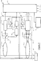
- Figure 1 schematically shows, in terms of functional blocks, a meter apparatus 100 according to an embodiment of the present invention.
- the meter apparatus 100 is preferably arranged for determining one or more parameters of an "Alternate Current” (AC) electric signal (hereinafter, AC signal) in one or more wires, preferably line L and neutral N wires of an electrical distribution system (the electrical distribution system being not shown).
- AC Alternate Current
- the line L and neutral N wires are preferably intended to supply electric power to one or more electric loads (for example, electric loads in residential households and buildings), such as the electric load 105.
- the electric load 105 may for example comprise a small appliance (such as personal computers, laser printers, battery chargers), the electric load 205 being for example powered by a "Switched-Mode Power Supply” (SMPS) module.
- SMPS Switchched-Mode Power Supply
- a SMPS module is typically configured for efficiently transferring electric power through the electrical distribution system to the electric load 205, while minimizing wasted energy by continually switching between low-dissipation, high-dissipation and no-dissipation states.
- the AC signal comprises an AC electric current (hereinafter, AC current) I AC through the L and neutral N wires and an AC electric voltage (hereinafter, AC voltage) V AC across the L and neutral N wires, and the AC signal parameters to be determined preferably comprise at least one among:
- the AC signal parameters may act as feedback information about energy consumption of the electric load 205, which can be used to promote energy awareness to residents. Indeed, timely electrical consumption feedback information through real-time metering may reduce electrical consumption by a fraction of 10-30% , and may lead to bill saving (indeed, the feedback information may be used to change energy consumption, for example by enabling the use of one or more appliances when it is least expensive).
- harmonic distortion typically affects electric loads powered by SMPS modules, and may cause, inter alia, large load currents in the neutral wire N of a three-phase electrical distribution system (which can cause potential fire hazards, as only the line wire L is usually protected by circuit breakers), overheating (which may shorten the life of the electronic devices), poor power factor of the electric loads (e.g. power factor lower than 0.9, which could result in monthly utility penalty fees), resonance (which produces over-current surges), false tripping of circuit breakers, and electric load malfunctions.
- Harmonic distortion typically affects electric loads powered by SMPS modules, and may cause, inter alia, large load currents in the neutral wire N of a three-phase electrical distribution system (which can cause potential fire hazards, as only the line wire L is usually protected by circuit breakers), overheating (which may shorten the life of the electronic devices), poor power factor of the electric loads (e.g. power factor lower than 0.9, which could result in monthly utility penalty fees), resonance (which produces over-current surges), false tripping of circuit
- the meter apparatus 100 in its widest conception preferably comprises:
- the meter apparatus 100 also comprises a current measurement section 110 configured for providing a signal V IS indicative of the AC current I AC (hereinafter, current measure signal V IS ) based on an inductive coupling with the line L and neutral N wires.
- a current measurement section 110 configured for providing a signal V IS indicative of the AC current I AC (hereinafter, current measure signal V IS ) based on an inductive coupling with the line L and neutral N wires.
- the current measurement section 110 is such that the current measure signal V IS is in a respective predetermined phase relationship (the current measure signal V IS being for example in phase) with respect to the AC current I AC
- the control unit 120 is also configured for determining the phase shift between the AC current I AC and the AC voltage V AC according to the phase shift between the current measure signal V IS from the current measurement section 110 and the first voltage measure signal V VS1 from the voltage measurement section 115 (and, when provided, according to the predetermined phase relationships).
- the control unit 120 (and, preferably, also the ADC module) is preferably supplied by means of one or more supply voltages V SUPPLY (for example including an upper supply voltage, e.g. +5V, and a lower supply voltage, e.g. -5V) with respect to a reference voltage (such as a 0V or ground voltage).
- V SUPPLY for example including an upper supply voltage, e.g. +5V, and a lower supply voltage, e.g. -5V
- a reference voltage such as a 0V or ground voltage
- the current measurement section 110 comprises a current sensing arrangement 110 CS for sensing the AC current I AC through the line L and neutral N wires based on said inductive coupling - the current sensing arrangement 110 CS , not limitative for the present invention, is illustrated as a generic oval block in the figure. More preferably, the current sensing arrangement 110 CS comprises a non-invasive (or non-intrusive) current sensor, the current sensing arrangement 110 CS being for example based on a current clamp device (not shown).
- a current clamp device is an electrical device having two jaws which open to allow clamping around a wire (e.g. the line wire L, as conceptually illustrated in the figure by the oval block 110 CS intercepting the line wire L ) .
- the current clamp device is (or comprises) a so-called split core current transformer.
- a split core current transformer comprises a split ring of ferrite or soft iron, and a wire coil wound round one or both halves, which form one winding of the current transformer - with the wire around which it is clamped (the line wire L in the example at issue) that forms the other winding.
- the clamped wire (the line wire L in the example at issue) forms the primary winding and the coil forms the secondary winding of the current transformer.
- the AC current sensed by the current sensing arrangement 110 CS (hereinafter, sensed current I S ) depends on the AC current I AC through the line L and neutral N wires and on the winding turns ratio of the current transformer.
- the current measurement section 110 also comprises a conversion module 110c for converting the sensed current I S into the current measure signal V IS , which is adapted to be processed by the control unit 120 for determining the AC signal parameters (as better discussed in the following).
- the current measure signal V IS is advantageously a voltage signal - in any case, the possibility that the ADC module of the control unit 120 carries out the conversion of a different electrical quantity, such as a current conversion, is not excluded, in which case the conversion module 110c may be omitted or simplified.
- the current measure signal V IS is adapted to (i.e., it is within) the full scale range at which the control unit 120 (and, particularly, the ADC module thereof) is allowed to operate (i.e.., between the upper and lower supply voltages).
- the conversion module 110c preferably comprises a voltage divider (e.g., a resistive voltage divider), not shown.
- the conversion module 110c preferably comprises a current divider (e.g., a resistive current divider), not shown.
- the current measure signal V IS features a predetermined phase relationship with respect to the AC current I AC (for example, by purposely adding the predetermined phase shift in the conversion module 110c ). Even more preferably, the current measure signal V IS is in phase with respect to the AC current I AC .
- the current measurement section 110 further comprises an energy harvesting module 110 H for harvesting energy from said inductive coupling (and, hence, from the sensed current I S ) when the conversion module 110c (and the subsequent processing by the control unit 120 ) is not enabled.
- the current measurement section 110 also comprises a power supply module 125 having one or more charge storage elements (not shown), such as a battery, a capacitor, or, preferably, as herein assumed, a super capacitor, for storing electric charge according to the harvested energy and for supplying such a stored electric charge to the control unit 120 (and, preferably, to the current 110 and voltage 115 measurement sections in a selective way, as discussed below) for powering thereof.
- charge storage elements not shown
- charge storage elements such as a battery, a capacitor, or, preferably, as herein assumed, a super capacitor, for storing electric charge according to the harvested energy and for supplying such a stored electric charge to the control unit 120 (and, preferably, to the current 110 and voltage 115 measurement sections in a selective way, as discussed
- the current measurement section 110 preferably comprises a switching device SW 110,A , which is preferably switchable (i.e., selectively operable) between a first configuration enabling electrical coupling (e.g., direct connection) between the current sensing arrangement 110 CS and the energy harvesting module 110 H thereby allowing energy harvesting from the sensed current I S , and a second configuration enabling electrical coupling (e.g., direct connection) between the current sensing arrangement 110 CS and the conversion module 110c thereby preventing energy harvesting and allowing conversion of the sensed current I S into the corresponding current measure signal V IS .
- a switching device SW 110,A which is preferably switchable (i.e., selectively operable) between a first configuration enabling electrical coupling (e.g., direct connection) between the current sensing arrangement 110 CS and the energy harvesting module 110 H thereby allowing energy harvesting from the sensed current I S
- a second configuration enabling electrical coupling (e.g., direct connection) between the current sensing arrangement 110
- the switching of the switching device SW 110,A in the first or second configuration is commanded by a command signal S 110 from the control unit 120, the command signal S 110 being for example a digital signal taking high or low logic levels (e.g. equal to the upper supply voltage or to the ground voltage, respectively).
- the command signal S 110 being for example a digital signal taking high or low logic levels (e.g. equal to the upper supply voltage or to the ground voltage, respectively).
- the current measurement section 110 also comprises a further switching device SW 110,B , which is preferably switchable (i.e., selectively operable) between a first, or open, configuration preventing electrical coupling between the power supply module 125 and the conversion module 110c (thus preventing powering, and hence operation, thereof) and a second, or closed, configuration enabling electrical coupling ( e.g., direct connection) between the power supply module 125 and the conversion module 110c (thus allowing operation thereof, and, hence, conversion of the sensed current I S into the current measure signal V IS ) .
- SW 110,B is preferably switchable (i.e., selectively operable) between a first, or open, configuration preventing electrical coupling between the power supply module 125 and the conversion module 110c (thus preventing powering, and hence operation, thereof) and a second, or closed, configuration enabling electrical coupling ( e.g., direct connection) between the power supply module 125 and the conversion module 110c (thus allowing operation thereof, and,
- the switching of the switching device SW 110,B in the open or closed configuration is commanded by the command signal S 110 (i.e., the same command signal S 110 that also commands the switching of the switching device SW 110,A ), so that the conversion module 110c is powered only when required, i.e. only when the sensed current I S has to be converted into the current measure signal V IS for determining the AC signal parameters.
- the command signal S 110 i.e., the same command signal S 110 that also commands the switching of the switching device SW 110,A
- the conversion module 110c is powered only when required, i.e. only when the sensed current I S has to be converted into the current measure signal V IS for determining the AC signal parameters.
- the voltage measurement section 115 comprises a voltage sensing arrangement 115vs for sensing the AC voltage V AC across the line L and neutral N wires - the voltage sensing arrangement 115vs, not limitative for the present invention, is illustrated as a generic oval block in the figure. More preferably, the voltage sensing arrangement 115vs comprises a non-invasive voltage sensor, being for example a voltage sensor based on capacitive coupling. In order to achieve that, as visible in the exemplary voltage sensing arrangement 115vs of Figure 3 , a first electrically conductive layer ECL L is preferably provided on the line wire L (i.e.
- first and second capacitive elements are formed which are associated with the line L and neutral N wires (i.e., with the sensed portions of the line L and neutral N wires), respectively.
- the first sensing capacitor is made up of the internal conductor IC L and the insulating layer IL L of the line wire L (i.e., of the sensed portion of the line wire L ) , and of the first electrically conductive layer ECL L ; the second sensing capacitor is instead made up of the internal conductor IC N and the insulating layer IL N of the neutral wire N (i.e., of the sensed portion of the neutral wire N ), and of the second electrically conductive layer ECL N .
- the sensed portion of the line wire L and the first electrically conductive layer ECL L act, respectively, as first and second terminals of the first sensing capacitor
- the sensed portion of the neutral wire N and the second electrically conductive layer ECL N act, respectively, as first and second terminals of the second sensing capacitor.
- the first ECL L and second ECL N electrically conductive layers are advantageously provided around the sensed portion of the line wire L and the sensed portion of the neutral wire N, respectively (so as to form cylindrical conductive layers), such that the first and second sensing capacitors result in cylindrical first and second capacitors - although this should not be construed in a restrictive manner.
- the first ECL L and second ECL N electrically conductive layers are copper sheets (or tapes). More preferably, the first ECL L and second ECL N electrically conductive layers are self-adhesive copper sheets adapted to be wrapped around the sensed portion of the line wire L and the sensed portion of the neutral wire N, respectively.
- the first ECL L and second ECL N electrically conductive layers preferably have same length and thickness.
- the length of the first ECL L and second ECL N electrically conductive layers is of the order of a few centimeters (for example between 1 cm and 5 cm, such as 1.25 cm), which descends from the measurement sensitivity achieved by the conditioning module 115c (as discussed below).
- This very short length of the first ECL L and second ECL N electrically conductive layers implies that the AC voltage V AC and/or the AC current I AC waveforms are determined independently from wire geometry (which may also significantly differ from a measure point to another one) and from wire spatial geometry or arrangement (i.e., regardless of whether the wire is bent or twisted).
- the thickness of the first ECL L and second ECL N electrically conductive layers is of the order of the hundredths of millimeters (for example, between 0.01 mm and 0.1 mm, such as 0.35 mm), so that when they are wrapped around the sensed portion of the line wire L and the sensed portion of the neutral wire N, respectively, substantially no additional space occupation arises.
- This very low space occupation of the first ECL L and second ECL N electrically conductive layers implies the adaptability of the voltage sensing arrangement 115vs (and, hence, of the meter apparatus 100 ) to substantially any measure point.
- first and second sensing capacitors are denoted by the references C 1 and C 2
- the first and second terminals of the first sensing capacitor C 1 are denoted by T 1C1 and T 2C1 , respectively
- first and second terminals of the second sensing capacitor C 2 are denoted by T 1C2 and T 2C2 , respectively.
- the first C 1 and second C 2 sensing capacitors feature a same capacitance value C S (although this should not be construed in a restrictive manner).
- a first voltage forms at the first electrically conductive layer ECL L (or, equivalently, at the second terminal T 2C1 of the first sensing capacitor C 1 ) according to the AC voltage V AC in the sensed portion of the line wire L and to the capacitance value Cs
- a second voltage forms at the second electrically conductive layer ECL N (or, equivalently, at the second terminal T 2C2 of the second sensing capacitor C 2 ) according to the AC voltage V AC in the sensed portion of the neutral wire N and to the capacitance value C S .
- the AC voltage V AC is applied between the first terminal T 1C1 of the first sensing capacitor C 1 and the first terminal T 1C2 of the second sensing capacitor C 2 , and that a respective voltage Vs (depending on the capacitance value C S ), hereinafter referred to as sensed voltage Vs, is applied between the second terminal T 2C1 of the first sensing capacitor C 1 and the second terminal T 2C2 of the second sensing capacitor C 2 - the differential nature of the sensed voltage Vs being also conceptually represented in Figures 1 and 3 by the arrow Vs across the output lines of the voltage sensing arrangement 115vs).
- the capacitance value Cs which depends on the wire size, is unknown a priori, as it depends on geometrical and electrical features of the wires at the measure point where the meter apparatus 100 is intended to be used.
- the amplitude of the AC voltage V AC (as well as the phase shift between AC voltage V AC and the AC current I AC , when the current measurement section 110 is provided) is independent from the capacitance value C S (or from the capacitance values, when different capacitance values for the first C 1 and second C 2 sensing capacitors are expected), and hence from the measure point.
- the voltage measurement section 115 preferably comprises a conditioning module 115c for receiving the sensed voltage Vs from the voltage sensing arrangement 115vs and for conditioning it into the voltage measure signals V VS1 , V VS2 , which are adapted to be processed by the control unit 120 (preferably, together with the current measure signal I AC ) for determining the AC signal parameters.
- a conditioning module 115c for receiving the sensed voltage Vs from the voltage sensing arrangement 115vs and for conditioning it into the voltage measure signals V VS1 , V VS2 , which are adapted to be processed by the control unit 120 (preferably, together with the current measure signal I AC ) for determining the AC signal parameters.
- the voltage measure signals V VS1 , V VS2 are advantageously voltage signals - in any case, the possibility that the ADC module of the control unit 120 carries out the conversion of a different electrical quantity, such as a current conversion, is not excluded, in which case the conditioning module 115c may be accordingly modified.
- the voltage measure signals V VS1 , V VS2 are single-ended voltage signals, i.e. voltage signals referred to proper reference voltages, and adapted to (i.e., it is within) the full scale range at which the ADC module of the control unit 120 is allowed to operate. Even more preferably, the voltage measure signals V VS1 , V VS2 are both referred to a common reference voltage, the common reference voltage being for example between the supply voltages V SUPPLY (such as the ground voltage).
- the conditioning module 115c comprises first and second conditioning branches (for the AC voltage V AC ) for providing the first V VS1 and second V VS2 voltage measure signals, respectively.
- the voltage measurement section 115 preferably comprises a switching device SW 115,A , which is preferably switchable between a first configuration electrically coupling the voltage sensing arrangement 115vs to the first conditioning branch of the conditioning module 115c (thereby allowing it to provide the first voltage measure signal V VS1 and, hence, allowing the control unit 120 to determine the phase shift between the AC current I AC and the AC voltage V AC according to the phase shift between the first voltage measure signal V VS1 and the current measure signal V IS ), and a second configuration electrically coupling the voltage sensing arrangement 115vs to the second branch of the conditioning module 115c (thereby allowing it to provide the second voltage measure signal V VS2 and, hence, allowing the control unit 120 to determine the capacitance value C S according to the first V VS1 and second V VS2 voltage measure signals, and the amplitude of the AC voltage V AC according to the first V VS1 or second V VS2 voltage measure signal, and to the determined capacitance value Cs, as detailed below).
- the first conditioning branch (for the AC voltage V AC ) preferably comprises a first sub-branch for receiving the AC voltage V AC + and a second sub-branch for receiving the AC voltage V AC - , and, more preferably, the second conditioning branch preferably comprises a first sub-branch for receiving the AC voltage V AC + and a second sub-branch for receiving the AC voltage V AC - .
- the switching device SW 115,A preferably comprises two switching elements, namely (as better illustrated in Figures 2A-2C ) a first switching element for electrically coupling the first sensing capacitor C 1 (and, hence, for providing the AC voltage V AC + ) to the first or second sub-branches of the first conditioning branch when the switching device SW 115,A takes the first or second configuration, respectively, and a second switching element for electrically coupling the second sensing capacitor C 2 (and, hence, for providing the AC voltage V AC - ) to the first or second sub-branches of the second conditioning branch when the switching device SW 115,A takes the first or second configuration, respectively.
- the conditioning module 115c (by enabling of the first sub-branches of the first and second conditioning branches) provides the first voltage measure signal V VS1
- the conditioning module 115c (by enabling of the second sub-branches of the first and second conditioning branches) provides the second voltage measure signal V VS2 .
- the switching of the switching device SW 115,A in the first or second configuration is commanded by a proper command signal S 115,A from the control unit 120, the command signal S 115,A being for example a digital signal (e.g., similar to the command signal S 110 ) .
- the command signal S 115,A preferably commands both the switching elements of the switching device SW 115,A concurrently.
- the voltage measurement section 115 also comprises a further switching device SW 115 , B , which is preferably switchable (i.e., selectively operable) between a first, or open, configuration preventing electrical coupling between the power supply module 125 and the conditioning module 115c (thus preventing powering, and hence operation, thereof) and a second, or closed, configuration enabling electrical coupling (e.g., direct connection) between the power supply module 125 and the conditioning module 115c (thus allowing operation thereof, and hence conditioning of the sensed voltage Vs into the corresponding voltage measure signals V VS1 ,V VS2 ) .
- a further switching device SW 115 , B which is preferably switchable (i.e., selectively operable) between a first, or open, configuration preventing electrical coupling between the power supply module 125 and the conditioning module 115c (thus preventing powering, and hence operation, thereof) and a second, or closed, configuration enabling electrical coupling (e.g., direct connection) between the power
- the switching of the switching device SW 115,B in the open or closed configuration is advantageously commanded by a command signal S 115,B different from the command signal S 115,A that commands the switching of the switching device SW 115,A , such that, regardless of the switching device SW 115,A configuration, the conditioning module 115c is energized only when required, i.e. only when the sensed voltage Vs has to be conditioned into the voltage measure signals V VS1 , V VS2 for determining the AC signal parameters.
- the command signals S 110 , S 115,B are synchronized to each other, e.g. such that the conversion module 110c in the current measurement section 110 and the conditioning module 115c in the voltage measurement section 115 are both powered (and, hence, enabled) during a predetermined measurement period (e.g., of the order of milliseconds or even second) in order to provide the current V IS and voltage V VS1 , V VS2 measure signals to the control unit 120 within a measurement time window (with the command signal S 115,A that, within the measurement period, sequentially enables the first and second sub-branches of the first and second conditioning branches for providing the voltage measure signals V VS1 , V VS2 ) .
- the command signals S 110 , S 115,B may also be independent from each other (at least in part).
- the conversion module 110c in the current measurement section 110 and the conditioning module 115c in the voltage measurement section 115 are both unpowered and hence disabled (switching devices SW 110,B and SW 115,B both in the open configuration), and the switching device SW 110,A in the second configuration enables energy harvesting by the energy harvesting module 110 H .
- the meter apparatus 100 preferably comprises a wireless network communication interface 130 for receiving the AC signal parameters determined by the control unit 120 (or an indication thereof) and for wirelessly transmitting them to a proper receiving apparatus (e.g., by means of short distance radio frequency technologies).
- the AC voltage V AC and/or the AC current I AC waveforms are determined by using inductive and capacitive couplings, thus in a non-intrusive manner (i.e., without altering the overall electric load of the electrical distribution system).
- the length of the first ECL L and second ECL N conductive layers, and hence of the sensing capacitors C 1 , C 2 thereby obtained may be very short (e.g., in the order of a few centimeters, such as 1.25cm).
- the very short length of the sensing capacitors C 1 , C 2 implies that the AC voltage V AC and/or the AC current I AC waveforms are determined independently from wire geometry (which may also significantly differ from a measure point to another one) and from wire spatial geometry or arrangement (i.e., regardless of whether the wire is bent or twisted), thus providing highly precise measurements.
- the proposed meter apparatus 100 features a simple circuit implementation requiring low cost hardware (as will be apparent from the following discussion of preferred embodiments of the conditioning module 115c illustrated in Figures 2A-2C ), so that it can profitably be implemented according to a multi-sensor approach - in any case, the simplicity and the efficiency of the meter apparatus 100 allows it to be implemented according to a single-sensor approach.
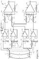
- FIG. 2A shows a circuit representation of the voltage measurement section 115, and particularly, of the conditioning module, according to a first embodiment of the present invention (the conditioning module according to this first embodiment of the present invention being denoted by 115c' for differentiating it from the conditioning modules of the following embodiments).
- the conditioning module 115 C ' is electrically coupled to the voltage sensing arrangement 115vs (that, as discussed above, is electrically represented by the first C 1 and second C 2 sensing capacitors, the AC voltage V AC (or substantially the AC voltage V AC ) being applied between the first terminals T 1C1 and T 1C2 thereof) by means of the switching device SW 115,A .
- the electronic components of the conditioning module 115c' have been considered referred to the ground voltage (as conceptually illustrated in the figure by the conventional electrical symbol of a ground terminal providing the ground voltage).
- the electronic components of the conditioning module 115c' (or at least a part thereof) may be referred to one or more different reference voltages (such the upper supply voltage and/or the lower supply voltage).
- the conditioning module 115 C ' comprises, in the first conditioning branch, a first input stage for processing (e.g., scaling) the AC voltage V AC and a first output stage for providing the first voltage measure signal V VS1 from the scaled AC voltage, and, in the second conditioning branch, a second input stage for processing the AC voltage V AC and a second output stage for providing the second voltage measure signal V VS2 from the processed AC voltage V AC (the specific implementation of the second input stage determining the processing on the AC voltage V AC ) .
- the first input stage comprises a first input capacitive element (e.g., a capacitor) C 3 having a first terminal T 1C3 electrically coupled to the second terminal T 2C1 of the first sensing capacitor C 1 when the switching device SW 115,A is in the first configuration (the first terminal T 1C3 of the first input capacitor C 3 being for example electrically floating when the switching device SW 115,A is in the second configuration), and a second terminal T 2C3 electrically coupled to the ground terminal, and a second input capacitive element (e.g., a capacitor) C 4 having a first terminal T 1C4 electrically coupled to the second terminal T 2C2 of the second sensing capacitor C 2 when the switching device SW 115,A is in the first configuration (the first terminal T 1C4 of the second input capacitor C 4 being for example electrically floating when the switching device SW 115,A is in the second configuration), and a second terminal T 2C4 electrically coupled to the ground terminal.
- a first input capacitive element e.g., a
- the first sensing capacitor C 1 and the first input capacitor C 3 define, when electrically coupled to each other, an impedance voltage divider, in particular a capacitive voltage divider for the AC voltage V AC +
- the second sensing capacitor C 2 and the second input capacitor C 4 define, when electrically coupled to each other, a capacitive voltage divider for the AC voltage V AC - (with the first C 1 and second C 2 sensing capacitors and, respectively, the first C 3 and second C 4 input capacitors that, when electrically coupled to each other, define as a whole a capacitive voltage divider for the AC voltage V AC ) .
- impedance voltage dividers other than the capacitive voltage dividers, such as inductive voltage dividers, resistive voltage dividers or a combination thereof.
- the first output stage of the conditioning module 115c' is arranged for providing the first voltage measure signal V VS1 according to a difference between the voltage V 1C3 from the first sub-branch of the first conditioning branch (or a voltage corresponding thereto) and the voltage V 1C4 from the first sub-branch of the second conditioning branch (or a voltage corresponding thereto).
- the differential amplifier circuit of the first output stage is conceived such that no phase shift is introduced in the first voltage measure signal V VS1 with respect to the voltages V 1C3 and V 1C4 (and, hence, with respect to the AC voltage V AC ) - in any case, as discussed above, the possibility that a predetermined phase shift is introduced in the first input stage and/or in the first output stage is not excluded.
- the differential amplifier circuit of the first output stage comprises:
- the first voltage measure signal V VS1 is (the resistance values of the resistors R 3 , R 4 , R 5 and R 6 being denoted by R 3 , R 4 , R 5 and R 6 , respectively):
- the first voltage measure signal V VS1 has no (or ideally no) phase shift with respect to the AC voltage V AC , such that the control unit 120 is allowed to determine the phase shift between the AC current I AC and the AC voltage V AC based on the current measure signal V IS and on the first voltage measure signal V VS1 - in any case, when a predetermined phase shift is introduced in the first input stage and/or in the first output stage, the control unit 120 is allowed to determine the phase shift between the AC current I AC and the AC voltage V AC also based on the predetermined phase shift.
- the phase shift between the AC current I AC and the AC voltage V AC is determined by the control unit 120 according to a zero-crossing technique.
- zero-crossing is a point where the sign of a function, such as a sinusoidal waveform, changes (e.g., from positive to negative or vice versa), and is defined by a crossing of the axis representing the zero value in the graph of the function.
- control unit 120 is configured for determining the zero-crossing of the current measure signal V IS (i.e., the time instant at which the current measure signal V IS is zero), and corresponding to the zero crossing of the AC current I AC (by virtue of the absence of phase shifting between the AC current I AC and the current measure signal V IS ), and the zero-crossing of the first voltage measure signal V VS1 (i.e., the time instant at which the first voltage measure signal V VS1 is zero), and corresponding to the zero crossing of the AC voltage V AC (by virtue of the absence of phase shifting between the AC voltage V AC and the first voltage measure signal V VS1 ), and the phase shift according to a difference between the time instant at which zero-crossing of the current measure signal V IS takes place and the time instant at which zero-crossing of the first voltage measure signal V VS1 takes place (the phase shift being expressed as time shift or angular shift).
- the meter apparatus 100 so far discussed allows determining the AC current I AC waveform and the phase shift between the AC voltage V AC and the AC current without the need of external power supply (indeed, thanks to the energy harvesting module 110 H , the meter apparatus 100 is a self-powering apparatus), with no direct electrical contact to the line L and neutral N wires (indeed, the current 110 CS and voltage 115vs sensing arrangements are "applied" externally to the wires, without direct physical contact with them in an intrusive manner, such as by interrupting or cutting the wires), and regardless of wire size, i.e.
- the capacitance value Cs which depend on the wire size, is not involved in determining the current measure signal V IS in the current measurement section 110, nor it affects the phase of the first voltage measure signal V VS1 in the voltage measurement section 115 thanks to the capacitive voltage dividers C 1 ,C 3 and C 2 ,C 4 and to the resistor-based differential amplifier circuit OA 1 ,R 3 -R 6 ).
- the first and second input stages comprise first R 1 ,R 2 and second R 7 ,R 8 input resistors electrically coupleable to the first C 1 and second C 2 sensing capacitors, respectively.
- the first input resistor R 1 has a first terminal T 1R1 electrically coupled to the second terminal T 2C1 of the first sensing capacitor C 1 when the switching device SW 115,A is in the second configuration (the first terminal T 1R1 of the first input resistor R 1 being for example electrically floating when the switching device SW 115,A is in the first configuration)
- the first input resistor R 2 has a first terminal T 1R2 electrically coupled (e.g., directly connected) to a second terminal T 2R1 of the first input resistor R 1 and a second terminal T 2R2 electrically coupled to the ground terminal.
- the second input resistor R 7 has a first terminal T 1R7 electrically coupled to the second terminal T 2C2 of the second sensing capacitor C 2 when the switching device SW 115,A is in the second configuration (the first terminal T 1R7 of the second input resistor R 7 being for example electrically floating when the switching device SW 115,A is in the first configuration), and the second input resistor R 8 has a first terminal T 1R8 electrically coupled (e.g., directly connected) to a second terminal T 2R7 of the second input resistor R 7 and a second terminal T 2R8 electrically coupled to the ground terminal.
- the first R 1 ,R 2 and second R 7 ,R 8 input resistors are in series to the first C 1 and second C 1 sensing capacitors, respectively, when the switching device SW 115,A is in the second configuration.
- the first sensing capacitor C 1 and the first input resistors R 1 ,R 2 define a high-pass filter for the AC voltage V AC +
- the second sensing capacitor C 2 and the second input resistors R 7 ,R 8 define a high-pass filter for the AC voltage V AC - (or, otherwise stated, the first C 1 and second C 2 sensing capacitors and, respectively, the first R 1 ,R 2 and second R 7 ,R 8 input resistors, when electrically coupled to each other, define as a whole a high-pass filter for the AC voltage V AC ) .
- the cut-off frequency f cut - off is sufficiently lower than 50Hz, so that the AC voltage V AC of the electrical mains is allowed to be transferred with a phase shift across the second sub-branches of the first and second conditioning branches (so that the resulting second voltage measure signal V VS2 has a phase shift with respect to the first voltage measure signal V VS1 , as better discussed below).
- the second output stage of the conditioning module 115c' is arranged for providing the second voltage measure signal V VS2 according to a difference between the voltage V 1R2 from the second sub-branch of the first conditioning branch and the voltage V 1R8 from the second sub-branch of the second conditioning branch.
- the differential amplifier circuit of the second output stage is conceived such that no phase shift is introduced in the second voltage measure signal V VS2 with respect to the voltages V 1R2 and V 1R8 (so that the phase of the second voltage measure signal V VS2 only depends on the phase ⁇ of the transfer function of the high-pass filter, whereby the control unit 120 is allowed to easily determine the, unknown, capacitance value C S of the first C 1 and second C 2 sensing capacitors, as discussed herebelow). In any case, nothing prevents from adding a further phase shift in the second output stage.
- the differential amplifier circuit of the second output stage is identical (e.g., in terms of architecture) to the differential amplifier circuit of the first output stage.
- the differential amplifier circuit of the second output stage comprises:
- the second voltage measure signal V VS2 is (the resistance values of the resistors R 9 , R 10 , R 11 and R 12 being denoted by R 9 , R 10 , R 11 and R 12 , respectively):
- V VS 2 V 1 R 2 R 10 R 9 + R 10 R 11 R 11 + R 12 ⁇ V 1 R 8
- the structure of the differential amplifier circuit of the second output stage is identical to the structure of the differential amplifier circuit of the first output stage (or substantially identical, as the possibility of including structural differences, e.g. for taking into account manufacturing tolerances or non-idealities of specific electronic components, is not excluded).
- the resistance values R 9 , R 10 , R 11 and R 12 of the resistors R 9 , Rio, R 11 and R 12 and the electrical properties of the respective operational amplifier OA 2 are preferably identical to the resistance values R 3 , R 4 , R 5 and R 6 of the resistors R 3 , R 4 , R 5 and R 6 and to the electrical properties of the operational amplifier OA 1 , respectively (or substantially identical, as the possibility of including structural differences, e.g. for taking into account manufacturing tolerances or non-idealities of specific electronic components, is not excluded).
- the second voltage measure signal V VS2 has a phase shift with respect to the first voltage measure signal V VS1 , which phase shift is detected and measured by the control unit 120 (e.g., still by means of the zero-crossing technique).
- phase shift which thus is known, depends on the capacitance value C I of the first C 3 and second C 4 input capacitors, which is known, and by the capacitance value C S of the first C 1 and second C 2 sensing capacitors, which instead is unknown (and depends, inter alia, on wire geometry).
- the control unit 120 upon reception of the first V VS1 and second V VS2 voltage measure signals, the control unit 120 is configured for determining the capacitance value C S according to the phase shift between the first V VS1 and second V VS2 voltage measure signals (e.g., by reversing the above equation for the phase ⁇ of the transfer function of the high-pass filter), and thus the amplitude of the AC voltage V AC according to the first V VS1 or second V VS2 voltage measure signals and to the capacitance value C S (e.g., by reversing the above equation for the first voltage measure signal V VS1 or for the second voltage measure signal V VS2 ) .
- the meter apparatus 100 is capable of determining the relevant AC signal parameters (namely, the amplitude of the AC current I AC , the amplitude of the AC voltage V AC and the phase shift between the AC current I AC and the AC voltage V AC ) regardless of wire geometry (namely, without calibration).
- both the first V VS1 and second V VS2 voltage measure signals depend on the amplitude of the AC voltage V AC and on the capacitance value Cs
- either the equation for first voltage measure signal V VS1 or the equation for the second voltage measure signal V VS2 may be reversed for determining the amplitude of the AC voltage V AC .
- the equation for the voltage measure signal to be reversed may be chosen according to the actual implementation of the conditioning module and/or according to design options and/or criteria (for example, the equation for the voltage measure signal implying lower computational capability may be reversed).
- the conditioning module 115c' preferably comprises one or more voltage stabilizing elements for stabilizing the voltages during their conditioning (so as to make the first V VS1 and/or second V VS2 voltage measure signals as precise as possible).
- one voltage stabilizing element for each sub-branch is provided.
- each voltage stabilizing element comprises a respective operational amplifier OA 3 -OA 6 in buffer configuration (hereinafter referred to as voltage buffer for the sake of conciseness).
- the voltage buffer OA 3 electrically couples the first terminal T 1C3 of the first input capacitor C 3 to the first terminal T 1R3 of the resistor R 3
- the voltage buffer OA 4 electrically couples the first terminal T 1R2 of the first input resistor R 2 to the first terminal T 1R9 of the resistor R 9
- the voltage buffer OA 5 electrically couples the first terminal T 1C4 of the second input capacitor C 4 to the first terminal T 1R5 of the resistor R 5
- the voltage buffer OA 6 electrically couples the first terminal T 1R8 of the second input resistor R 8 to the first terminal T 1R11 of the resistor R 11 .
- FIG. 2B a circuit representation of a conditioning module 115c" according to a second embodiment of the present invention is shown.
- the conditioning module 115c" is almost entirely similar to the conditioning module 115 C ', for which reason same elements will not be discussed again.
- the conditioning module 115c" differs from the conditioning module 115c' in that the first and second input stages comprise, instead of the high-pass filter (defined by the first C 1 and second C 2 sensing capacitors and, respectively, the first R 1 ,R 2 and second R 7 ,R 8 input resistors, as discussed above), an impedance voltage divider for the AC voltage V AC .
- the impedance voltage divider is advantageously a capacitive voltage divider.
- the first input stage comprises a further first input capacitive element, e.g. a capacitor (hereinafter referred to as first input capacitor, for the sake of conciseness) C 5 electrically coupleable to the first sensing capacitor C 1 and, preferably, the second input stage comprises a further second input capacitive element, e.g. a capacitor (hereinafter referred to as second input capacitor, for the sake of conciseness) C 6 electrically coupleable to the second sensing capacitor C 2 .
- first input capacitor hereinafter referred to as first input capacitor, for the sake of conciseness
- the first C 1 and second C 2 sensing capacitors and, respectively, the first C 5 and second C 6 input capacitors define, when coupled to each other, an impedance voltage divider for the AC voltage V AC (i.e., a first capacitive voltage divider Ci,Cs for the AC voltage V AC + and a second capacitive voltage divider C 2 ,C 6 for the AC voltage V AC ) .
- the first input capacitor C 5 has a first terminal Tics electrically coupled to the second terminal T 2C1 of the first sensing capacitor C 1 when the switching device SW 115,A is in the second configuration (the first terminal Tics of the first input capacitor C 5 being for example electrically floating when the switching device SW 115,A is in the first configuration) and to the resistor R 9 (for example, by interposition of the voltage buffer OA 4 ), and a second terminal Tics electrically coupled ( e.g., directly connected) to the ground terminal.
- the second input capacitor C 6 has a first terminal T 1C6 electrically coupled to the second terminal T 2C2 of the second sensing capacitor C 2 when the switching device SW 115,A is in the second configuration (the first terminal T 1C6 of the second input capacitor C 6 being for example electrically floating when the switching device SW 115,A is in the first configuration) and to the resistor R 11 (for example, by interposition of the voltage buffer OA 6 ), and a second terminal T 2C6 electrically coupled to the ground terminal.
- V VS2 V 1 C 5
- the structure (as well as the values and the electrical properties of electronic components) of the differential amplifier circuit of the second output stage is preferably identical to the structure (and, respectively, to the values and the electrical properties of electronic components) of the differential amplifier circuit of the first output stage (or substantially identical, as the possibility of including structural differences, e.g.
- the first voltage measure signal V VS1 is (the resistance values of the resistors R 3 , R 4 , R 5 and R 6 being denoted by R 3 , R 4 , R 5 and R 6 , respectively):
- the second voltage measure signal V VS2 is in phase (i.e., it has no, or substantially no, phase shift) with respect to the first voltage measure signal V VS1 , so that the capacitance value C S can be easily determined based on the first V VS1 and second V VS2 voltage measure signals (i.e., based on the amplitudes thereof as detected by the control unit 120, as discussed herebelow).
- the provision of predetermined phase shifts to the first voltage measure signal V VS1 and/or to the second voltage measure signal V VS2 , and/or to the current measure signal V IS does not affect the principles of the present invention.
- the control unit 120 upon reception of the first V VS1 and second V VS2 voltage measure signals, the control unit 120 is configured for determining the capacitance value C S according to a difference between the first V VS1 and second V VS2 voltage measure signals (i.e., according to the amplitudes thereof detected by the control unit 120), e.g.
- the capacitance values C I and C IN are advantageously set different from each other (in order to avoid numerator zeroing and, hence, the impossibility of determining the capacitance value C S itself).
- the meter apparatus 100 is capable of determining the relevant AC signal parameters (namely, the amplitude of the AC current I AC , the amplitude of the AC voltage V AC and the phase shift between the AC current I AC and the AC voltage V AC ) regardless of the size of the wires (namely, without calibration because of the size of the wires).
- the conditioning module 115c" allows avoiding the determination of the phase shift between the first V VS1 and second V VS2 voltage measure signals, which could be a relevant source of error in some applications.
- FIG. 2C shows a circuit representation of a conditioning module 115c ′′′ according to a third embodiment of the present invention.
- the conditioning module 115c ′′′ is almost entirely similar to the conditioning module 115c', for which reason same elements will not be discussed again.
- the conditioning module 115c ′′′ differs from the conditioning module 115c' in that it comprises, instead of the high-pass filter (which, in the conditioning module 115c', is defined by the first C 1 and second C 2 sensing capacitors and, respectively, the first R 1 ,R 2 and second R 7 ,R 8 input resistors, as discussed above), a differentiator arrangement for the AC voltage V AC .
- the high-pass filter which, in the conditioning module 115c', is defined by the first C 1 and second C 2 sensing capacitors and, respectively, the first R 1 ,R 2 and second R 7 ,R 8 input resistors, as discussed above
- the first and second input stages comprise first R 13 and second R 14 input resistors electrically coupleable to the first C 1 and second C 2 sensing capacitors, respectively, and first OA 7 and second OA 8 operational amplifiers electrically coupled to the first R 13 and second R 14 input resistors, respectively (the operational amplifiers OA 7 , OA 8 preferably having same electrical characteristics, for example the same electrical characteristics as the operational amplifiers OA 1 -OA 6 and being preferably powered with the supply voltages V SUPPLY upon closing of the switching device SW 115,B ).
- the first input resistor R 13 has a first terminal T 1R13 electrically coupled ( e.g., electrically connected) to the second terminal T 2C1 of the first sensing capacitor C 1 when the switching device SW 115,A is in the second configuration (the first terminal T 1R13 of the first input resistor R 13 being for example electrically floating when the switching device SW 115,A is in the first configuration) and electrically coupled ( e.g., electrically connected) to a an inverting input terminal of the first operational amplifier OA 7 , and a second terminal T 2R13 electrically coupled ( e.g., electrically connected) to an output terminal of the first operational amplifier OA 7 and electrically coupled to the first terminal T 1R9 of the resistor R 9 (for example, by interposition of the voltage buffer OA 4 ).
- the first input resistor R 13 is electrically coupled ( e.g., electrically connected) across the (inverting) input terminal and the output terminal of the first operational amplifier OA 7 (with the non-inverting input terminal of the first operational amplifier OA 7 that is instead electrically coupled, e.g. electrically connected, to the ground terminal).
- the second input resistor R 14 has a first terminal T 1R14 electrically coupled ( e.g., electrically connected) to the second terminal T 2C2 of the second sensing capacitor C 2 when the switching device SW 115,A is in the second configuration (the first terminal T 1R14 of the second input resistor R 14 being for example electrically floating when the switching device SW 115,A is in the first configuration) and electrically coupled ( e.g., electrically connected) to a an inverting input terminal of the first operational amplifier OA 8 , and a second terminal T 2R14 electrically coupled ( e.g., electrically connected) to an output terminal of the second operational amplifier OA 8 and electrically coupled to the first terminal T 1R11 of the resistor R 11 (for example, by interposition of the voltage buffer OA 6 ).
- the second input resistor R 14 is electrically coupled ( e.g., electrically connected) across the (inverting) input terminal and the output terminal of the second operational amplifier OA 8 (with the non-inverting input terminal of the second operational amplifier OA 8 that is instead electrically coupled, e.g. electrically connected, to the ground terminal).
- the first sensing capacitor C 1 , the first input resistor R 13 and the first operational amplifier OA 7 define a differentiator arrangement (or differentiator) for the AC voltage V AC +
- the second sensing capacitor C 2 , the second input resistor R 14 and the second operational amplifier OA 8 define a differentiator for the AC voltage V AC (or, otherwise stated, the first C 1 and second C 2 sensing capacitors and, respectively, the first R 13 and second R 14 input resistors and the associated first OA 7 and second OA 8 operational amplifiers, when electrically coupled to each other, define as a whole a differentiator for the AC voltage V AC ) .
- circuit arrangements other than those formed by the operational amplifiers OA 7 , OA 8 and the input resistors R 13 ,R 14 can be used to for implementing the differentiator.
- V 2 R 14 ⁇ R IN C S dV AC ⁇ dt
- the second voltage measure signal V VS2 resulting from the conditioning module 115 C ′′′ is (the resistance values of the resistors R 9 , Rio, R 11 and R 12 being again denoted by R 9 , R 10 , R 11 and R 12 , respectively):
- V AC A sin 2 ⁇ ft wherein A is the amplitude of the AC voltage V AC to be determined
- V VS2 ⁇ R IN C S A 2 ⁇ f cos 2 ⁇ ft R 10 R 9 + R 10 R 11 R 11 + R 12 ⁇ R 12 R 11
- the structure (as well as the values and the electrical properties of electronic components) of the differential amplifier circuit of the second output stage is preferably identical to the structure (and, respectively, to the values and the electrical properties of electronic components) of the differential amplifier circuit of the first output stage (or substantially identical, as the possibility of including structural differences, e.g.
- the first voltage measure signal V VS1 is (the resistance values of the resistors R 3 , R 4 , R 5 and R 6 being denoted by R 3 , R 4 , R 5 and R 6 , respectively):
- V VS 1 C S C S + C I A ( sin 2 ⁇ ft V VS 2 R IN C S A 2 ⁇ f cos 2 ⁇ ft
- the capacitance value C S can be easily determined based on the first V VS1 and second V VS2 voltage measure signals (i.e., based on the amplitudes thereof as detected by the control unit 120) from the above equations.
- the control unit 120 upon reception of the first V VS1 and second V VS2 voltage measure signals, the control unit 120 is configured for determining the capacitance value C S according to a difference between the first V VS1 and second V VS2 voltage measure signals, e.g.
- the amplitude A of the AC voltage V AC is advantageously determined by taking into account a number of samples, the samples being preferably sufficiently far from the "risky" points in which the above equation is not valid (e.g., ⁇ /6, ⁇ /4, ⁇ /3 and k ⁇ /20).
- the meter apparatus 100 is capable of determining the relevant AC signal parameters (namely, the amplitude of the AC current I AC , the amplitude of the AC voltage V AC and the phase shift between the AC current I AC and the AC voltage V AC ) regardless of the size of the wires (namely, without calibration because of the size of the wires).
- the conditioning module 115c ′′′ allows avoiding the determination of the phase shift between the first V VS1 and second V VS2 voltage measure signals, which could be a relevant source of error in some applications. In particular, this approach significantly improves the amplitude measurement with an error lower than 5%.
- the conditioning module 115c wherein the ADC module should exhibit a very high sensitivity (i.e., a resolution of the order of ⁇ V) thus determining relatively high complexity and costs
- the conditioning module 115 C ′′′ allows achieving very low costs and reliability.
Landscapes
- Physics & Mathematics (AREA)
- General Physics & Mathematics (AREA)
- Engineering & Computer Science (AREA)
- Power Engineering (AREA)
- Measuring Instrument Details And Bridges, And Automatic Balancing Devices (AREA)
- Measurement Of Current Or Voltage (AREA)
- Investigating Or Analyzing Materials By The Use Of Electric Means (AREA)
- Measurement Of Resistance Or Impedance (AREA)
Claims (14)
- Messeinrichtung (100) zum Bestimmen von Parametern eines elektrischen AC-Signals in einem ersten (L) und einem zweiten (N) Draht, wobei das elektrische AC-Signal einen elektrischen AC-Strom (IAC ) und eine elektrische AC-Spannung (VAC ) umfasst, wobei die Messeinrichtung (100) Folgendes umfasst:einen Messbereich (115), der zum Bereitstellen eines ersten (VVS1 ) und eines zweiten (VVS2 ) Messsignals ausgelegt ist, von denen jedes die elektrische AC-Spannung (VAC ) auf Basis einer ersten kapazitiven Kopplung (C1 ) mit dem ersten Draht (L) undeiner zweiten kapazitiven Kopplung (C2 ) mit dem zweiten Draht (N) anzeigt, wobei das erste (VVS1 ) und das zweite (VVS2 ) Messsignal von Kapazitätswerten der ersten (C1 ) und der zweiten (C2 ) kapazitiven Kopplung abhängig sind,ein erstes (C1 ) und ein zweites (C2 ) kapazitives Element zum Durchführen der ersten und der zweiten kapazitiven Kopplung undeine Steuereinheit (120), die zu Folgendem ausgelegt ist:Bestimmen der Kapazitätswerte der ersten (C1 ) und der zweiten (C2 ) kapazitiven Kopplung gemäß dem ersten (VVS1 ) und dem zweiten (VVS2 ) Messsignal undBestimmen der Amplitude der elektrischen AC-Spannung (VAC ) gemäß dem ersten (VVS1 ) oder dem zweiten (VVS2 ) Messsignal und gemäß den Kapazitätswerten der ersten (C1 ) und der zweiten (C2 ) kapazitiven Kopplung,wobei der Messbereich (115) ferner ein erstes (C3 ) und ein zweites (C4 ) kapazitives Eingangselement umfasst, die an das erste (C1 ) bzw. das zweite (C2 ) kapazitive Element elektrisch koppelbar sind, wobei das erste (C1 ) und das zweite (C2 ) kapazitive Element bzw. das erste (C3 ) und das zweite (C4 ) kapazitive Eingangselement, wenn sie aneinandergekoppelt sind, einen Impedanzspannungsteiler (C1,C3 ; C2,C4 ) zum Bereitstellen des ersten Messsignals (VVS1 ) aus der elektrischen AC-Spannung (VAC ) definieren, wobei das erste Messsignal (VVS1 ) mit Bezug auf die elektrische AC-Spannung (VAC ) in Phase ist.
- Messeinrichtung (100) nach Anspruch 1, die ferner einen weiteren Messbereich (110) umfasst, der zum Bereitstellen eines dritten Messsignals (VIS ) ausgelegt ist, das auf Basis einer induktiven Kopplung mit dem ersten (L) oder dem zweiten (N) Draht den elektrischen AC-Strom (IAC ) anzeigt, wobei die Steuereinheit (120) ferner zu Folgendem ausgelegt ist:
Bestimmen einer Phasenverschiebung zwischen der elektrischen AC-Spannung (VAC ) und dem elektrischen AC-Strom (IAC ) gemäß einer Phasenverschiebung zwischen dem ersten (VVS1 ) und dem dritten (VIS ) Messsignal. - Messeinrichtung (100) nach Anspruch 1 oder 2, wobei das erste (C1 ) und das zweite (C2 ) kapazitive Element mindestens einen Abschnitt des ersten (L) und des zweiten (N) Drahts umfassen.
- Messeinrichtung (100) nach einem der vorhergehenden Ansprüche, wobei der Messbereich (115) ein weiteres erstes (C5 ) und ein weiteres zweites (C6 ) kapazitives Element umfasst, die an das erste (C1 ) bzw. das zweite (C2 ) kapazitive Element elektrisch koppelbar sind, wobei das erste (C1 ) und das zweite (C2 ) kapazitive Element bzw. das weitere erste (C5 ) und das weitere zweite (C6 ) kapazitive Element, wenn sie aneinandergekoppelt sind, einen Impedanzspannungsteiler (C1,C5 ; C2,C6 ) definieren, der das zweite Messsignal (VVS2 ) aus der elektrischen AC-Spannung (VAC ) bereitstellt, wobei das erste (VVS1 ) und das zweite (VVS2 ) Messsignal mit Bezug aufeinander in Phase sind.
- Messeinrichtung (100) nach einem der Ansprüche 1 bis 3, wobei der Messbereich (115) eine erste (R13,OA7 ) und eine zweite (R14,OA8 ) Schaltungsanordnung umfasst, die an das erste (C1 ) bzw. das zweite (C2 ) kapazitive Element elektrisch koppelbar sind, wobei das erste (C1 ) und das zweite (C2 ) kapazitive Element bzw. die erste (R13,OA7 ) und die zweite (R14,OA8 ) Schaltungsanordnung, wenn sie aneinandergekoppelt sind, eine Differenziereranordnung definieren, die das zweite Messsignal (VVS2 ) aus der elektrischen AC-Spannung (VAC ) bereitstellt.
- Messeinrichtung (100) nach Anspruch 4 oder 5, wobei die Steuereinheit (120) zum Bestimmen der Kapazitätswerte der ersten (C1 ) und der zweiten (C2 ) kapazitiven Kopplung gemäß den Amplituden des ersten (VVS1 ) und des zweiten (VVS2 ) Messsignals sowie zum Bestimmen der Amplitude der elektrischen AC-Spannung (VAC ) gemäß den Amplituden des ersten (VVS1 ) oder des zweiten (VVS2 ) Messsignals und den Kapazitätswerten der ersten (C1 ) und der zweiten (C2 ) kapazitiven Kopplung angeordnet ist.
- Messeinrichtung (100) nach einem der Ansprüche 1 bis 3, wobei das erste (VVS1 ) und das zweite (VVS2 ) Messsignal eine Phasenverschiebung mit Bezug aufeinander aufweisen, wobei die Phasenverschiebung zwischen dem ersten (VVS1 ) und dem zweiten (VVS2 ) Messsignal von den Kapazitätswerten der ersten (C1 ) und der zweiten (C2 ) kapazitiven Kopplung abhängig ist und wobei die Steuereinheit (120) ferner zu Folgendem angeordnet ist:Bestimmen der Phasenverschiebung zwischen dem ersten (VVS1 ) und dem zweiten (VVS2 ) Messsignal,Bestimmen der Kapazitätswerte der ersten (C1 ) und der zweiten (C2 ) kapazitiven Kopplung gemäß der Phasenverschiebung zwischen dem ersten (VVS1 ) und dem zweiten (VVS2 ) Messsignal undBestimmen der Amplitude der elektrischen AC-Spannung (VAC ) gemäß dem ersten (VVS1 ) oder dem zweiten (VVS2 ) Messsignal und den Kapazitätswerten der ersten (C1 ) und der zweiten (C2 ) kapazitiven Kopplung.
- Messeinrichtung (100) nach Anspruch 7, wobei der Messbereich (115) ein erstes (R1 ,R2 ) und ein zweites (R7 ,R8 ) Widerstandselement umfasst, die an das erste (C1 ) bzw. das zweite (C2 ) kapazitive Element elektrisch koppelbar sind, wobei das erste (C1 ) und das zweite (C2 ) kapazitive Element bzw. das erste (R1 ,R2 ) und das zweite (R7 ,R8 ) Widerstandselement, wenn sie aneinandergekoppelt sind, ein Hochpassfilter definieren, das das zweite Messsignal (VVS2 ) aus der elektrischen AC-Spannung (VAC ) bereitstellt.
- Messeinrichtung (100) nach einem der Ansprüche 2 bis 8, sofern abhängig von Anspruch 2, wobei der weitere Messbereich (110) ein Energieerntemodul (110H ) zum Ernten von Energie von der induktiven Kopplung und eine Schaltvorrichtung (SW110,A ), die in einer ersten Auslegung, die das Energieernten durch die Energieernteeinheit (110H ) erlaubt, oder in einer zweiten Auslegung, die die Bereitstellung des dritten Messsignals (VIS ) erlaubt und das Energieernten verhindert, selektiv betreibbar ist.
- Messeinrichtung (100) nach Anspruch 9, wobei der weitere Messbereich (110) ein Ladungsspeicherelement (125) zum Speichern einer elektrischen Ladung gemäß dem Energieernten und zum Zuführen der elektrischen Ladung zum Messbereich (115), zum weiteren Messbereich (110) und zur Steuereinheit (120) umfasst.
- Messeinrichtung (100) nach einem der Ansprüche 2 bis 10, sofern von Anspruch 2 abhängig, wobei der weitere Messbereich (110) eine Stromzangenvorrichtung (110cs ) zum Durchführen der induktiven Kopplung mit dem ersten (L) und dem zweiten (N) Draht umfasst.
- Messeinrichtung (100) nach Anspruch 11, wobei die Stromzangenvorrichtung einen Kabelumbaustromwandler umfasst.
- Messeinrichtung (100) nach einem der Ansprüche 3 bis 12, sofern von Anspruch 3 abhängig, wobei der Messbereich (115) eine erste (ECLL ) und eine zweite (ECLN) elektrisch leitfähige Schicht umfasst, die angepasst sind, auf Abschnitten des ersten (L) bzw. des zweiten (N) Drahts bereitgestellt zu sein, und wobei der Abschnitt des ersten Drahts (L) und die erste elektrisch leitfähige Schicht (ECLL ) darauf das erste kapazitive Element (C1 ) zwischen dem ersten Draht (L) und dem Messbereich (115) definieren und der Abschnitt des zweiten Drahts (N) und die zweite elektrisch leitfähige Schicht (ECLN) darauf das zweite kapazitive Element (C2 ) zwischen dem zweiten Draht (N) und dem Messbereich (115) definieren.
- Verfahren zum Bestimmen von Parametern eines elektrischen AC-Signals in einem ersten (L) und einem zweiten (N) Draht, wobei das elektrische AC-Signal einen elektrischen AC-Strom (IAC ) und eine elektrische AC-Spannung (V AC ) umfasst, wobei das Verfahren Folgendes umfasst:Bereitstellen eines ersten (VVS1 ) und eines zweiten (VVS2 ) Messsignals, von denen jedes die elektrische AC-Spannung (VAC ) auf Basis einer ersten kapazitiven Kopplung (C1 ) mit dem ersten Draht (L) und einer zweiten kapazitiven Kopplung (C2 ) mit dem zweiten Draht (N) anzeigt, wobei das erste (WS1 ) und das zweite (VVS2 ) Messsignal von Kapazitätswerten der ersten (C1 ) und der zweiten (C2 ) kapazitiven Kopplung abhängig sind, Bestimmen der Kapazitätswerte der ersten (C1 ) und der zweiten (C2 ) kapazitiven Kopplung gemäß dem ersten (VVS1 ) und dem zweiten (VVS2 ) Messsignal undBestimmen der Amplitude der elektrischen AC-Spannung (V AC ) gemäß dem ersten (VVS1 ) oder dem zweiten (VVS2 ) Messsignal undden Kapazitätswerten der ersten (C1 ) und der zweiten (C2 ) kapazitiven Kopplung,wobei das Verfahren ferner Folgendes umfasst:Bereitstellen eines ersten (C1 ) und eines zweiten (C2 ) kapazitiven Elements zum Durchführen der ersten und der zweiten kapazitiven Kopplung,Bereitstellen eines ersten (C3 ) und eines zweiten (C4 ) kapazitiven Eingangselements, die an das erste (C1 ) bzw. das zweite (C2 ) kapazitive Element elektrisch koppelbar sind, wobei das erste (C1 ) und das zweite (C2 ) kapazitive Element bzw. das erste (C3 ) und das zweite (C4 ) kapazitive Eingangselement, wenn sie aneinandergekoppelt sind, einen Impedanzspannungsteiler (C1,C3; C2,C4 ) zum Bereitstellen des ersten Messsignals (VVS1 ) aus der elektrischen AC-Spannung (VAC ) definieren, wobei das erste Messsignal (VVS1 ) mit Bezug auf die elektrische AC-Spannung (VAC ) in Phase ist.
Applications Claiming Priority (1)
| Application Number | Priority Date | Filing Date | Title |
|---|---|---|---|
| PCT/EP2016/062303 WO2017207037A1 (en) | 2016-05-31 | 2016-05-31 | Meter apparatus for measuring parameters of electrical quantity |
Publications (3)
| Publication Number | Publication Date |
|---|---|
| EP3465232A1 EP3465232A1 (de) | 2019-04-10 |
| EP3465232B1 true EP3465232B1 (de) | 2022-07-06 |
| EP3465232B8 EP3465232B8 (de) | 2022-09-14 |
Family
ID=56203312
Family Applications (1)
| Application Number | Title | Priority Date | Filing Date |
|---|---|---|---|
| EP16731809.6A Active EP3465232B8 (de) | 2016-05-31 | 2016-05-31 | Messvorrichtung zur messung von parametern elektrischer grösse |
Country Status (4)
| Country | Link |
|---|---|
| US (1) | US11280810B2 (de) |
| EP (1) | EP3465232B8 (de) |
| CN (1) | CN109791168B (de) |
| WO (1) | WO2017207037A1 (de) |
Families Citing this family (10)
| Publication number | Priority date | Publication date | Assignee | Title |
|---|---|---|---|---|
| KR102127459B1 (ko) * | 2019-02-28 | 2020-06-29 | 주식회사 알아이파워 | 무선 전력 측정 시스템 및 방법 |
| FI20196025A1 (en) | 2019-11-28 | 2021-05-29 | Safegrid Oy | Power converter for harvesting electrical power |
| CN112305351A (zh) * | 2020-10-20 | 2021-02-02 | 云南电网有限责任公司电力科学研究院 | 一种泄漏电流重构电压的moa阻性电流测量方法 |
| CN112305348A (zh) * | 2020-10-20 | 2021-02-02 | 云南电网有限责任公司电力科学研究院 | 一种考虑同相电容型设备重构moa阻性电流快速测试方法 |
| CN112305349A (zh) * | 2020-10-20 | 2021-02-02 | 云南电网有限责任公司电力科学研究院 | 一种moa阻性电流快速测量方法 |
| CN112305352A (zh) * | 2020-10-20 | 2021-02-02 | 云南电网有限责任公司电力科学研究院 | 一种基于同相电容型设备的电压重构moa阻性电流测试方法 |
| CN114916235B (zh) * | 2020-12-08 | 2026-03-31 | 华为数字能源技术有限公司 | 交流电能检测装置 |
| CN115343515B (zh) * | 2022-10-17 | 2023-03-07 | 基合半导体(宁波)有限公司 | 模拟前端电路、电容测量电路、芯片及电子设备 |
| DE102024107596A1 (de) * | 2024-03-18 | 2025-09-18 | SAX Power GmbH | Induktiver Stromwandler, Smart-Meter und Verfahren zur Messung elektrischer Größen in einem elektrischen Leiter |
| CN120820750B (zh) * | 2025-09-12 | 2025-12-09 | 绵阳师范学院 | 一种非接触式轨道移频信号在线监测方法及系统 |
Family Cites Families (8)
| Publication number | Priority date | Publication date | Assignee | Title |
|---|---|---|---|---|
| US5473244A (en) * | 1992-09-17 | 1995-12-05 | Libove; Joel M. | Apparatus for measuring voltages and currents using non-contacting sensors |
| JP3761470B2 (ja) | 2001-04-04 | 2006-03-29 | 北斗電子工業株式会社 | 非接触電圧計測方法及び装置並びに検出プローブ |
| GB0709893D0 (en) * | 2007-05-23 | 2007-07-04 | Onzo Ltd | Apparatus for monitoring rescue consumption |
| FR2940457B1 (fr) | 2008-12-18 | 2011-02-18 | Schneider Electric Ind Sas | Dispositif diviseur capacitif, capteur de tension, module de declencheur et appareil de protection electrique pourvus d'un tel dispositif |
| JP5460929B2 (ja) * | 2010-09-29 | 2014-04-02 | シーメンス アクチエンゲゼルシヤフト | 入力電流を出力電圧に変換するためのコンバータ、当該コンバータを備えた装置、および、入力電流を出力電圧に変換するための方法 |
| CN103649688B (zh) * | 2011-06-30 | 2017-02-22 | 迈普尔平版印刷Ip有限公司 | 用于电容式测量系统的有源屏蔽 |
| US9151818B2 (en) * | 2011-11-08 | 2015-10-06 | Analog Devices Global | Voltage measurement |
| US10120055B2 (en) * | 2014-08-28 | 2018-11-06 | Siemens Industry, Inc. | Isolated capacitance line voltage sensor |
-
2016
- 2016-05-31 WO PCT/EP2016/062303 patent/WO2017207037A1/en not_active Ceased
- 2016-05-31 EP EP16731809.6A patent/EP3465232B8/de active Active
- 2016-05-31 US US16/304,220 patent/US11280810B2/en active Active
- 2016-05-31 CN CN201680087418.8A patent/CN109791168B/zh active Active
Also Published As
| Publication number | Publication date |
|---|---|
| US11280810B2 (en) | 2022-03-22 |
| EP3465232A1 (de) | 2019-04-10 |
| EP3465232B8 (de) | 2022-09-14 |
| US20200278383A1 (en) | 2020-09-03 |
| CN109791168B (zh) | 2021-12-10 |
| CN109791168A (zh) | 2019-05-21 |
| WO2017207037A1 (en) | 2017-12-07 |
Similar Documents
| Publication | Publication Date | Title |
|---|---|---|
| US11280810B2 (en) | Meter apparatus for measuring parameters of electrical quantity | |
| CN209150714U (zh) | 基于全电子式互感器的一二次融合智能断路器 | |
| WO2010103332A1 (en) | Current measuring device | |
| US10161983B2 (en) | Method and system for hot socket detection in a utility meter | |
| US20140028463A1 (en) | Methods and systems for detection of sensor tampering | |
| CN110703023B (zh) | 配电线路智能计量测量装置 | |
| CN111487466A (zh) | 一种电流互感器二次回路直流电阻带电检测装置 | |
| CN202994957U (zh) | 线路故障指示装置 | |
| CN102590610B (zh) | 智能一体式多功能电能表及其对负载的控制方法 | |
| Balsamo et al. | Non-intrusive zigbee power meter for load monitoring in smart buildings | |
| CN102323461A (zh) | 单元多户智能电能表箱 | |
| CN109212308A (zh) | 智能断路器 | |
| CN109406919A (zh) | 线损检测设备和线损检测系统 | |
| Nordman et al. | A wireless sensor concept for managing electrical distribution networks | |
| CN102608414B (zh) | 高压电气开关设备的嵌入式电能计量方法及扩展应用方法 | |
| JP5767673B2 (ja) | 電流波形測定装置 | |
| CN101650379A (zh) | 组合式传感器 | |
| Brunelli et al. | Non-invasive voltage measurement in a three-phase autonomous meter | |
| Schmid et al. | Application of non conventional voltage and currents sensors in high voltage transmission and distribution systems | |
| CN114079259A (zh) | 一种保护装置 | |
| CN208860902U (zh) | 一种分压电路参数检测电路及电能计量芯片 | |
| CN104049141B (zh) | 智能一体式多功能电能表对负载的控制方法 | |
| JP2016090447A (ja) | 電力測定装置および電力測定システム | |
| CN214895575U (zh) | 一种电路电量采集器 | |
| CN116008897A (zh) | 一种电能表计量电流互感器监测装置 |
Legal Events
| Date | Code | Title | Description |
|---|---|---|---|
| STAA | Information on the status of an ep patent application or granted ep patent |
Free format text: STATUS: THE INTERNATIONAL PUBLICATION HAS BEEN MADE |
|
| PUAI | Public reference made under article 153(3) epc to a published international application that has entered the european phase |
Free format text: ORIGINAL CODE: 0009012 |
|
| STAA | Information on the status of an ep patent application or granted ep patent |
Free format text: STATUS: REQUEST FOR EXAMINATION WAS MADE |
|
| 17P | Request for examination filed |
Effective date: 20181228 |
|
| AK | Designated contracting states |
Kind code of ref document: A1 Designated state(s): AL AT BE BG CH CY CZ DE DK EE ES FI FR GB GR HR HU IE IS IT LI LT LU LV MC MK MT NL NO PL PT RO RS SE SI SK SM TR |
|
| AX | Request for extension of the european patent |
Extension state: BA ME |
|
| RAP1 | Party data changed (applicant data changed or rights of an application transferred) |
Owner name: TELECOM ITALIA S.P.A. Owner name: ALMA MATER STUDIORUM - UNIVERSITA DI BOLOGNA |
|
| DAV | Request for validation of the european patent (deleted) | ||
| DAX | Request for extension of the european patent (deleted) | ||
| GRAP | Despatch of communication of intention to grant a patent |
Free format text: ORIGINAL CODE: EPIDOSNIGR1 |
|
| STAA | Information on the status of an ep patent application or granted ep patent |
Free format text: STATUS: GRANT OF PATENT IS INTENDED |
|
| INTG | Intention to grant announced |
Effective date: 20220329 |
|
| GRAS | Grant fee paid |
Free format text: ORIGINAL CODE: EPIDOSNIGR3 |
|
| GRAA | (expected) grant |
Free format text: ORIGINAL CODE: 0009210 |
|
| STAA | Information on the status of an ep patent application or granted ep patent |
Free format text: STATUS: THE PATENT HAS BEEN GRANTED |
|
| AK | Designated contracting states |
Kind code of ref document: B1 Designated state(s): AL AT BE BG CH CY CZ DE DK EE ES FI FR GB GR HR HU IE IS IT LI LT LU LV MC MK MT NL NO PL PT RO RS SE SI SK SM TR |
|
| REG | Reference to a national code |
Ref country code: AT Ref legal event code: REF Ref document number: 1503228 Country of ref document: AT Kind code of ref document: T Effective date: 20220715 Ref country code: CH Ref legal event code: EP |
|
| REG | Reference to a national code |
Ref country code: DE Ref legal event code: R096 Ref document number: 602016073324 Country of ref document: DE |
|
| REG | Reference to a national code |
Ref country code: IE Ref legal event code: FG4D |
|
| REG | Reference to a national code |
Ref country code: DE Ref legal event code: R081 Ref document number: 602016073324 Country of ref document: DE Owner name: TELECOM ITALIA S.P.A., IT Free format text: FORMER OWNERS: ALMA MATER STUDIORUM - UNIVERSITA DI BOLOGNA, BOLOGNA, IT; TELECOM ITALIA S.P.A., MILANO, IT |
|
| REG | Reference to a national code |
Ref country code: CH Ref legal event code: PK Free format text: BERICHTIGUNG B8 |
|
| RAP2 | Party data changed (patent owner data changed or rights of a patent transferred) |
Owner name: TELECOM ITALIA S.P.A. |
|
| REG | Reference to a national code |
Ref country code: LT Ref legal event code: MG9D |
|
| REG | Reference to a national code |
Ref country code: NL Ref legal event code: MP Effective date: 20220706 |
|
| PG25 | Lapsed in a contracting state [announced via postgrant information from national office to epo] |
Ref country code: SE Free format text: LAPSE BECAUSE OF FAILURE TO SUBMIT A TRANSLATION OF THE DESCRIPTION OR TO PAY THE FEE WITHIN THE PRESCRIBED TIME-LIMIT Effective date: 20220706 Ref country code: RS Free format text: LAPSE BECAUSE OF FAILURE TO SUBMIT A TRANSLATION OF THE DESCRIPTION OR TO PAY THE FEE WITHIN THE PRESCRIBED TIME-LIMIT Effective date: 20220706 Ref country code: PT Free format text: LAPSE BECAUSE OF FAILURE TO SUBMIT A TRANSLATION OF THE DESCRIPTION OR TO PAY THE FEE WITHIN THE PRESCRIBED TIME-LIMIT Effective date: 20221107 Ref country code: NO Free format text: LAPSE BECAUSE OF FAILURE TO SUBMIT A TRANSLATION OF THE DESCRIPTION OR TO PAY THE FEE WITHIN THE PRESCRIBED TIME-LIMIT Effective date: 20221006 Ref country code: NL Free format text: LAPSE BECAUSE OF FAILURE TO SUBMIT A TRANSLATION OF THE DESCRIPTION OR TO PAY THE FEE WITHIN THE PRESCRIBED TIME-LIMIT Effective date: 20220706 Ref country code: LV Free format text: LAPSE BECAUSE OF FAILURE TO SUBMIT A TRANSLATION OF THE DESCRIPTION OR TO PAY THE FEE WITHIN THE PRESCRIBED TIME-LIMIT Effective date: 20220706 Ref country code: LT Free format text: LAPSE BECAUSE OF FAILURE TO SUBMIT A TRANSLATION OF THE DESCRIPTION OR TO PAY THE FEE WITHIN THE PRESCRIBED TIME-LIMIT Effective date: 20220706 Ref country code: FI Free format text: LAPSE BECAUSE OF FAILURE TO SUBMIT A TRANSLATION OF THE DESCRIPTION OR TO PAY THE FEE WITHIN THE PRESCRIBED TIME-LIMIT Effective date: 20220706 Ref country code: ES Free format text: LAPSE BECAUSE OF FAILURE TO SUBMIT A TRANSLATION OF THE DESCRIPTION OR TO PAY THE FEE WITHIN THE PRESCRIBED TIME-LIMIT Effective date: 20220706 |
|
| REG | Reference to a national code |
Ref country code: AT Ref legal event code: MK05 Ref document number: 1503228 Country of ref document: AT Kind code of ref document: T Effective date: 20220706 |
|
| PG25 | Lapsed in a contracting state [announced via postgrant information from national office to epo] |
Ref country code: PL Free format text: LAPSE BECAUSE OF FAILURE TO SUBMIT A TRANSLATION OF THE DESCRIPTION OR TO PAY THE FEE WITHIN THE PRESCRIBED TIME-LIMIT Effective date: 20220706 Ref country code: IS Free format text: LAPSE BECAUSE OF FAILURE TO SUBMIT A TRANSLATION OF THE DESCRIPTION OR TO PAY THE FEE WITHIN THE PRESCRIBED TIME-LIMIT Effective date: 20221106 Ref country code: HR Free format text: LAPSE BECAUSE OF FAILURE TO SUBMIT A TRANSLATION OF THE DESCRIPTION OR TO PAY THE FEE WITHIN THE PRESCRIBED TIME-LIMIT Effective date: 20220706 Ref country code: GR Free format text: LAPSE BECAUSE OF FAILURE TO SUBMIT A TRANSLATION OF THE DESCRIPTION OR TO PAY THE FEE WITHIN THE PRESCRIBED TIME-LIMIT Effective date: 20221007 |
|
| REG | Reference to a national code |
Ref country code: DE Ref legal event code: R097 Ref document number: 602016073324 Country of ref document: DE |
|
| PG25 | Lapsed in a contracting state [announced via postgrant information from national office to epo] |
Ref country code: SM Free format text: LAPSE BECAUSE OF FAILURE TO SUBMIT A TRANSLATION OF THE DESCRIPTION OR TO PAY THE FEE WITHIN THE PRESCRIBED TIME-LIMIT Effective date: 20220706 Ref country code: RO Free format text: LAPSE BECAUSE OF FAILURE TO SUBMIT A TRANSLATION OF THE DESCRIPTION OR TO PAY THE FEE WITHIN THE PRESCRIBED TIME-LIMIT Effective date: 20220706 Ref country code: DK Free format text: LAPSE BECAUSE OF FAILURE TO SUBMIT A TRANSLATION OF THE DESCRIPTION OR TO PAY THE FEE WITHIN THE PRESCRIBED TIME-LIMIT Effective date: 20220706 Ref country code: CZ Free format text: LAPSE BECAUSE OF FAILURE TO SUBMIT A TRANSLATION OF THE DESCRIPTION OR TO PAY THE FEE WITHIN THE PRESCRIBED TIME-LIMIT Effective date: 20220706 Ref country code: AT Free format text: LAPSE BECAUSE OF FAILURE TO SUBMIT A TRANSLATION OF THE DESCRIPTION OR TO PAY THE FEE WITHIN THE PRESCRIBED TIME-LIMIT Effective date: 20220706 |
|
| PLBE | No opposition filed within time limit |
Free format text: ORIGINAL CODE: 0009261 |
|
| STAA | Information on the status of an ep patent application or granted ep patent |
Free format text: STATUS: NO OPPOSITION FILED WITHIN TIME LIMIT |
|
| PG25 | Lapsed in a contracting state [announced via postgrant information from national office to epo] |
Ref country code: SK Free format text: LAPSE BECAUSE OF FAILURE TO SUBMIT A TRANSLATION OF THE DESCRIPTION OR TO PAY THE FEE WITHIN THE PRESCRIBED TIME-LIMIT Effective date: 20220706 Ref country code: EE Free format text: LAPSE BECAUSE OF FAILURE TO SUBMIT A TRANSLATION OF THE DESCRIPTION OR TO PAY THE FEE WITHIN THE PRESCRIBED TIME-LIMIT Effective date: 20220706 |
|
| 26N | No opposition filed |
Effective date: 20230411 |
|
| PG25 | Lapsed in a contracting state [announced via postgrant information from national office to epo] |
Ref country code: AL Free format text: LAPSE BECAUSE OF FAILURE TO SUBMIT A TRANSLATION OF THE DESCRIPTION OR TO PAY THE FEE WITHIN THE PRESCRIBED TIME-LIMIT Effective date: 20220706 |
|
| P01 | Opt-out of the competence of the unified patent court (upc) registered |
Effective date: 20230528 |
|
| P02 | Opt-out of the competence of the unified patent court (upc) changed |
Effective date: 20230530 |
|
| PG25 | Lapsed in a contracting state [announced via postgrant information from national office to epo] |
Ref country code: SI Free format text: LAPSE BECAUSE OF FAILURE TO SUBMIT A TRANSLATION OF THE DESCRIPTION OR TO PAY THE FEE WITHIN THE PRESCRIBED TIME-LIMIT Effective date: 20220706 |
|
| REG | Reference to a national code |
Ref country code: CH Ref legal event code: PL |
|
| PG25 | Lapsed in a contracting state [announced via postgrant information from national office to epo] |
Ref country code: MC Free format text: LAPSE BECAUSE OF FAILURE TO SUBMIT A TRANSLATION OF THE DESCRIPTION OR TO PAY THE FEE WITHIN THE PRESCRIBED TIME-LIMIT Effective date: 20220706 |
|
| REG | Reference to a national code |
Ref country code: BE Ref legal event code: MM Effective date: 20230531 |
|
| PG25 | Lapsed in a contracting state [announced via postgrant information from national office to epo] |
Ref country code: MC Free format text: LAPSE BECAUSE OF FAILURE TO SUBMIT A TRANSLATION OF THE DESCRIPTION OR TO PAY THE FEE WITHIN THE PRESCRIBED TIME-LIMIT Effective date: 20220706 Ref country code: LU Free format text: LAPSE BECAUSE OF NON-PAYMENT OF DUE FEES Effective date: 20230531 Ref country code: LI Free format text: LAPSE BECAUSE OF NON-PAYMENT OF DUE FEES Effective date: 20230531 Ref country code: CH Free format text: LAPSE BECAUSE OF NON-PAYMENT OF DUE FEES Effective date: 20230531 |
|
| REG | Reference to a national code |
Ref country code: IE Ref legal event code: MM4A |
|
| PG25 | Lapsed in a contracting state [announced via postgrant information from national office to epo] |
Ref country code: IE Free format text: LAPSE BECAUSE OF NON-PAYMENT OF DUE FEES Effective date: 20230531 |
|
| PG25 | Lapsed in a contracting state [announced via postgrant information from national office to epo] |
Ref country code: IE Free format text: LAPSE BECAUSE OF NON-PAYMENT OF DUE FEES Effective date: 20230531 |
|
| PG25 | Lapsed in a contracting state [announced via postgrant information from national office to epo] |
Ref country code: BE Free format text: LAPSE BECAUSE OF NON-PAYMENT OF DUE FEES Effective date: 20230531 |
|
| PG25 | Lapsed in a contracting state [announced via postgrant information from national office to epo] |
Ref country code: BG Free format text: LAPSE BECAUSE OF FAILURE TO SUBMIT A TRANSLATION OF THE DESCRIPTION OR TO PAY THE FEE WITHIN THE PRESCRIBED TIME-LIMIT Effective date: 20220706 |
|
| PG25 | Lapsed in a contracting state [announced via postgrant information from national office to epo] |
Ref country code: BG Free format text: LAPSE BECAUSE OF FAILURE TO SUBMIT A TRANSLATION OF THE DESCRIPTION OR TO PAY THE FEE WITHIN THE PRESCRIBED TIME-LIMIT Effective date: 20220706 |
|
| PGFP | Annual fee paid to national office [announced via postgrant information from national office to epo] |
Ref country code: DE Payment date: 20250519 Year of fee payment: 10 |
|
| PGFP | Annual fee paid to national office [announced via postgrant information from national office to epo] |
Ref country code: GB Payment date: 20250527 Year of fee payment: 10 |
|
| PGFP | Annual fee paid to national office [announced via postgrant information from national office to epo] |
Ref country code: IT Payment date: 20250530 Year of fee payment: 10 |
|
| PGFP | Annual fee paid to national office [announced via postgrant information from national office to epo] |
Ref country code: FR Payment date: 20250526 Year of fee payment: 10 |
|
| PG25 | Lapsed in a contracting state [announced via postgrant information from national office to epo] |
Ref country code: CY Free format text: LAPSE BECAUSE OF FAILURE TO SUBMIT A TRANSLATION OF THE DESCRIPTION OR TO PAY THE FEE WITHIN THE PRESCRIBED TIME-LIMIT; INVALID AB INITIO Effective date: 20160531 |
|
| PG25 | Lapsed in a contracting state [announced via postgrant information from national office to epo] |
Ref country code: HU Free format text: LAPSE BECAUSE OF FAILURE TO SUBMIT A TRANSLATION OF THE DESCRIPTION OR TO PAY THE FEE WITHIN THE PRESCRIBED TIME-LIMIT; INVALID AB INITIO Effective date: 20160531 |
|
| PG25 | Lapsed in a contracting state [announced via postgrant information from national office to epo] |
Ref country code: TR Free format text: LAPSE BECAUSE OF FAILURE TO SUBMIT A TRANSLATION OF THE DESCRIPTION OR TO PAY THE FEE WITHIN THE PRESCRIBED TIME-LIMIT Effective date: 20220706 |