EP3458878B1 - Particle detector made of a semiconductor material - Google Patents
Particle detector made of a semiconductor material Download PDFInfo
- Publication number
- EP3458878B1 EP3458878B1 EP17723993.6A EP17723993A EP3458878B1 EP 3458878 B1 EP3458878 B1 EP 3458878B1 EP 17723993 A EP17723993 A EP 17723993A EP 3458878 B1 EP3458878 B1 EP 3458878B1
- Authority
- EP
- European Patent Office
- Prior art keywords
- layer
- central part
- type
- doping
- peripheral part
- Prior art date
- Legal status (The legal status is an assumption and is not a legal conclusion. Google has not performed a legal analysis and makes no representation as to the accuracy of the status listed.)
- Active
Links
Images


Classifications
-
- G—PHYSICS
- G01—MEASURING; TESTING
- G01T—MEASUREMENT OF NUCLEAR OR X-RADIATION
- G01T1/00—Measuring X-radiation, gamma radiation, corpuscular radiation, or cosmic radiation
- G01T1/29—Measurement performed on radiation beams, e.g. position or section of the beam; Measurement of spatial distribution of radiation
-
- G—PHYSICS
- G01—MEASURING; TESTING
- G01T—MEASUREMENT OF NUCLEAR OR X-RADIATION
- G01T1/00—Measuring X-radiation, gamma radiation, corpuscular radiation, or cosmic radiation
- G01T1/16—Measuring radiation intensity
- G01T1/26—Measuring radiation intensity with resistance detectors
Definitions
- the technical field of the invention is that of detectors. More particularly, the invention relates to a detector intended to measure a beam of particles or an environment of particles.
- these detectors are made in the thickness of a silicon wafer and can therefore reach a thickness substantially equal to 300 ⁇ m. They therefore absorb a non-negligible amount of radiation. The primary consequence of this absorption is to greatly disturb the beam during the measurement. In addition, since the radiation of matter interactions take place in a large volume of the material making up the detector, the degradation of the electrical and mechanical characteristics of the latter can be very rapid. Finally charges are created outside the active area and diffuses to the electrodes adding noise to the measurement signal.
- the placement of electrodes in the path of the beam remains essential.
- the presence of these electrodes has two consequences.
- the materials used for the manufacture of these electrodes absorb a non-negligible amount of the beam.
- the structure of the detector must be completely between the electrodes.
- the active area is mainly concentrated in the intrinsic area of the semiconductor material. In other words, a large part of the material through which the beam passes does not contribute directly to detection.
- a device for measuring a particle beam according to the preamble of claim 1 is known from EP 0 736 780 A1 (RIKAGAKU ⁇ ENKYUSHO [JP]; SUMITOMO ELECTRIC INDUSTRIES [JP]; ISHIKAWAJI) October 9, 1996.
- the invention offers a solution to the problems mentioned above by providing a detection device in which the beam only crosses the useful area of the detector, the structure allowing the collection of the charges generated by the beam in the active area being offset laterally by relative to the path of the beam to be measured.
- the peripheral part surrounds the central part so that a particle beam can pass through the central part without passing through the peripheral part, an orifice being formed at the rear face, in a region of the central part so that the thickness of said region of the central part along an axis normal to the front face is less than the thickness of the peripheral part along said normal axis.
- Particle beam means in particular a beam of neutrons or a beam of X-rays. In other words, the notion of particles must be taken here in its broad sense.
- the particle beam to be measured only crosses the active zone of the device, that is to say, the zone of charge space.
- the disturbance generated by the detector on the beam is thus minimized.
- the beam does not pass through the part of the device by which charge collection is carried out, the measurement noise is greatly reduced.
- the beam passes not only the active part, but also the areas of the device through which the charges generated by the beam are collected.
- the beam can also create unwanted charges in these collection zones. Unlike the charges created in the active area which are driven by the electric field, the unwanted charges will be driven by a diffusion phenomenon. This diffusion of charges unwanted signals will produce a spurious signal which affects the accuracy of the measurement.
- the beam does not cross the zones in charge of collecting carriers, these zones not being located on the path of the beam.
- the signal obtained therefore makes it possible to carry out more precise and less noisy measurements than the devices according to the state of the art.
- the reduction of interactions to the active area alone allows a substantial decrease in the temperature of the detector linked to these.
- the presence of an orifice at the rear face makes it possible to ensure that the thickness traversed by the beam is limited to the thickness of the active area while obtaining good mechanical strength through of the thicker peripheral area.
- the device according to one aspect of the invention may have one or more complementary characteristics among the following, considered individually or according to all the technically possible combinations.
- the central part is made of a large gap semiconductor material in order to accept large doses of high energy particles.
- the semiconductor is silicon carbide.
- large gap is meant a gap whose energy is at least twice as great as the energy of the silicon gap.
- the charge space zone is formed using a Schottky diode allowing a rapid response of the recovery of direct-reverse behavior, a PN diode then taking advantage of the tunnel effect or a PIN diode allowing good quality of the tensile strength.
- At least one interface facing the orifice arranged in the rear (or front) face is structured so as to favor the absorption, the transmission or the reflection of one or more wavelengths.
- interface is meant a boundary between two materials (or two layers). It can therefore be the boundary between two constituent materials (or two layers) of the device or a boundary between the device and its environment (the surface of the bottom of the orifice for example) or the front face.
- structured is meant the fact that the interface has reliefs forming a pattern (pyramid, truncated pyramid, paving stone, etc.) whose dimensions are determined as a function of the wavelength whose absorption is desired, the structuring constituting a diffraction network sometimes called "photonic crystal".
- absorption transmission or reflection
- absorption, transmission or reflection is meant that, for a given device, the absorption, transmission or reflection coefficient of the wavelength considered with the structuring is greater than the absorption coefficient , transmission or reflection without structuring, everything else being equal.
- metal balls are present in the central part of the detection device, preferably opposite the orifice provided in the rear face, said balls being distributed in a periodic structure so to form a plasmon network.
- the space loading area of the central part is only located in the region of the central part opposite the orifice.
- the active area is limited to the area effectively crossed by the beam.
- the space loading area of the central part extends beyond the region of the central part opposite the orifice.
- MIS semiconductor Insulating Metal
- one of the layers forming the Schottky diode being metallic, it is possible to collect a type of charge carrier by this same layer, which eliminates at least one deposition step and facilitates the manufacture of the device compared to a zone d charging space produced by a diode.
- the third layer of a material makes it possible to collect a type of charge carrier.
- this layer being located only at the peripheral part, it does not disturb the beam.
- the third layer of a material makes it possible to collect a type of charge carrier.
- this layer being located only at the peripheral part, it does not disturb the beam.
- the active area is limited to the area actually crossed by the beam, the collection of charges from the active area to the anode being effected using the eighth layer.
- the peripheral part comprises a fifth layer of a semiconductor material doped in a first type of doping, the doping level of the fifth layer being higher than the doping level of the first layer, the fifth layer being located between the third layer and the first layer of the peripheral part.
- the first orifice is defined by a side wall and by a bottom and a layer of an oxide covers the side wall and the bottom of the first orifice.
- the section of the first orifice and / or of the second orifice is of circular or square shape.
- the first orifice and the second orifice are positioned in the center of the device.
- the expression “positioned in the center of the device” means here that when the device and the orifice are projected onto a surface perpendicular to the direction of the stack, the projection of the orifice onto this surface is centered relative to the projection of the device.
- the fourth layer covers only part of the second layer.
- the absorption of the beam by the fourth layer is limited while ensuring charge collection from the active area towards the anode.
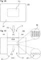
- a first embodiment of the invention illustrated in Figure 1A and 1B relates to a device 100 for measuring a particle beam FS comprising a first part, called the central part PC, a second part, called the peripheral part PP.
- the central part PC comprises means for forming a space charge zone ZCE (in dotted lines on all the figures) intended to be crossed by a beam of particles FS to be measured, charge carriers of a first type and of a second type being generated by said beam FS when the latter crosses the space charge zone ZCE.
- the peripheral part PP comprises means for collecting at least one type of charge carrier from the first type or the second type of charge carriers generated at the level of the space charge zone ZCE.
- the peripheral part PP surrounds the central part PC so that a particle beam FS can pass through the central part PC without passing through the peripheral part PP.
- the device according to the invention makes it possible to measure a beam of particles FS by minimizing the disturbances generated by the measurement on the output beam FS '.
- Such a configuration makes it possible in particular to reduce the amount of radiation absorbed by the device and therefore the number of interactions between material radiation likely to disturb the measurement or degrade the measurement device.
- the measuring device 100 comprises a front face F and a rear face B, the front face F being parallel to the rear face B, and in that an orifice O1 is formed at the level of the face rear B, in a region of the central part PC so that the thickness of said region of the central part PC along an axis normal to the front face F is less than the thickness of the peripheral part PP along said normal axis.
- the orifice O1 can be circular, rectangular or even square. More generally, it can take the form of any polygon.
- the size of the orifice O1 is determined by the size of the beam to be measured. Preferably, the width of the beam is less than the width of the orifice O1.
- the width of the central region can therefore vary from a micron to ten centimeters.
- the entire central part PC is opposite the orifice O1.
- the area of the central part PC is equal to the area of a section of the orifice O1.
- At least one interface opposite the orifice O1 arranged in the rear face B is structured so as to favor the absorption, transmission or reflection of one or more wavelengths.
- This is in particular due to the fact that the ST structuring thus created will favor the harvesting of certain photons (in the case of UV radiation in particular) and therefore the absorption of radiation whose wavelength corresponds to said photons.
- the dimensions of the structures are generally of the same order of magnitude as the dimensions of the wavelength that it is sought to target, that is to say of the order of a few hundred nanometers, for example 200 to 300 nm.
- the device 100 can therefore, in addition to detection, help to filter the incident FS beam. It is therefore possible to obtain a detection device 100 which reads the intensity of the beam FS over a given length for which the absorption coefficient is high, for example greater than or equal to 90%, while absorbing little one or more other wavelengths for which the absorption coefficient is low, for example less than or equal to 10%.
- metal BI balls for example gold, aluminum BI balls
- the BI beads are distributed in a periodic structure so as to form a plasmon network. As the FS beam passes, electromagnetic resonances will occur at the level of the periodic structure thus formed, making it possible to increase the absorption coefficient of the material comprising said balls BI (and therefore of the device 100) for one or more lengths of selected wave.
- the wavelengths affected by the periodic structure are a function of the geometric parameters of said structure, in particular the size of the balls BI and the distance between the balls in the three dimensions of space.
- the central part PC is centered with respect to the whole of the device 100.
- the central part PC and / or the peripheral part PP of the component can be made, at least in part, from a large-gap semiconductor material , for example silicon carbide, diamond or a semiconductor alloy composed of elements from column III-V or II-VI.
- a large-gap semiconductor material for example silicon carbide, diamond or a semiconductor alloy composed of elements from column III-V or II-VI.
- the semiconductor is diamond
- p doping can be obtained by implantation of boron atoms and n doping by implantation of phosphorus atoms.
- the p doping can be by implantation of boron atoms and the n doping by implantation of nitrogen atoms.
- the space charge zone ZCE of the central part PC is only located in the region of the central part PC opposite the orifice O1.
- the space charge zone ZCE of the central part PC extends beyond the region of the central part PC opposite the orifice O1.
- the central part PC comprises a first layer 1 of a semiconductor material; and a second layer 2 of a conductive material covering the first layer 1.
- the ZCE charge space zone is formed by the Schottky diode formed by the first layer 1 and the second layer 2, l orifice O1 being formed in the first layer 1.
- the orifice O1 formed in the first layer 1 of the central part PC can be produced by an engraving technique of the RIE type.
- the peripheral part PP comprises a third layer 3 'of a conductive material; a first layer 1 'of a semiconductor material covering the third layer 3' and arranged in continuity with the first layer 1 of the central part PC; and a second layer 2 ′ of a conductive material covering the first layer 1 and arranged in continuity with the second layer 2 of the central part PC.
- the ZCE space charge zone is formed by the Schottky diode constituted by the first layer 1 of a conductive material and the second layer 2 of a semiconductor material.
- the ZCE space charge area is therefore located on the central PC part but also on the peripheral PP part.
- the third layer 3 'of a conductive material ensures the collection of a first type of charge carriers generated in the charge space charge zone ZCE while the first layer 2.2' made of a material conductor, collects a second type of charge carrier generated in the ZCE space charge zone.
- the second layer 2.2 ′ and the third layer 3.3 ′ may consist of a metal such as copper, zinc or gold or alternatively of monolayer or multilayer graphene.
- Nickel, aluminum, titanium or tungsten can also be used. More generally, any conductive material adapted to the manufacturing or operating conditions of the device can be chosen.
- the material used for the second layer 2.2 ′ may be different from the material used for the third layer 3.3 ′.
- the materials used for the third layer 3 ′ can be chosen so as to obtain ohmic contact between the third layer 3 ′ and the first layer 1 ′ of the peripheral part PP.
- the doping level of the first layer 1 of the central part PC is identical to the doping level of the first layer 1 ′ of the peripheral part.
- the manufacturing process is thereby facilitated because it requires only one level of doping.
- the doping level of the first layer 1 of the central part PC is lower than the doping level of the first layer 1 'of the peripheral part. This configuration ensures a better distribution of the electric field and therefore the use of higher voltages for the polarization of the detector.
- the first layer 1.1 ′ has a thickness of between 500 nm and 50 microns.
- the second layer 2, 2 ′ has a thickness of between 50 nm and 200 nm, preferably substantially equal to 100 nm.
- the central part PC comprises a first layer 1 of a semiconductor material doped in a first type of doping; a second layer 2 of a semiconductor material doped in a second type of doping opposite to the first type of doping, said second layer 2 covering the first layer 1; and a fourth layer 4 of a conductive material, said fourth layer 4 covering the second layer 2.
- the charge space zone ZCE is formed by the PN diode formed by the first layer 1 and the second layer 2, the orifice O1 being formed in the first layer 1.
- the orifice O1 formed in the first layer 1 of the central part PC can be produced by an etching technique of the RIE type.
- the peripheral part PP comprises a third layer 3 'of a conductive material; a first layer 1 'of a semiconductor material doped in a first type of doping covering the third layer 3' and arranged in continuity with the first layer 1 of the central part PC; a second layer 2 'of a semiconductor material doped in a second type of doping opposite to the first type of doping covering the first layer 1', said second layer 2 'being arranged in continuity with the second layer 2 of the part central PC; and a fourth layer 4 'of a conductive material, said fourth layer 4' covering the second layer 2 ', said fourth layer 4' being arranged in continuity with the fourth layer 4 of the PC part.
- the doping of the first layer 1,1 ' is of type n
- the doping of the second layer 2,2' is of type p.
- the space load area ZCE is formed by the PN diode constituted by the first layer 1,1 'of a semiconductor material doped in a first type of doping and the second layer 2,2' of a semiconductor material doped in a second type doping opposite to the first type of doping.
- the ZCE load space zone is therefore located on the central PC part but also on the peripheral PP part.
- the third layer 3 ′ of the peripheral part collects a first type of charge carriers generated in the space charge zone ZCE while the fourth layer 4,4 ′, made of a conductive material, collects a second type of charge carrier generated in the ZCE space charge zone.
- the third layer 3 ′ and the fourth layer 4,4 ′ can be constituted by a metal such as copper, zinc or gold or even by mono or multilayer graphene. Nickel, aluminum, titanium or tungsten can also be used. More generally, any conductive material suitable for the manufacturing or operating conditions of the device can be chosen.
- the material used for the third layer 3 ′ may be different from the material used for the fourth layer 4,4 ′.
- the materials used for the third layer 3 'can be chosen so as to obtain an ohmic contact between the third layer 3' and the first layer 1 'of the peripheral part PP.
- the materials used for the fourth layer 4,4 'can be chosen so as to obtain an ohmic contact between the fourth layer 4,4' and the second layer 2,2 '.
- the doping level of the first layer 1 of the central part PC is identical to the doping level of the first layer 1 ′ of the peripheral part PP.
- the doping level of the second layer 2 of the central part PC is identical to the doping level of the second layer 2 'of the peripheral part. As explained above, the manufacturing process is made easier because it requires only one level of doping.
- the doping of the first layer 1,1 ' is of type n and the doping of the second layer 2,2' is of type p.
- the doping level of the first layer 1.1 ′ is between 5.10 14 and 5.10 19 atoms per cm 3 , of preferably substantially equal to 5.10 15 atoms per cm 3 .
- the doping level of the second layer 2.2 ′ is between 1.10 16 and 5.10 19 atoms per cm 3 , preferably substantially equal to 1.10 19 atoms per cm 3 .
- the doping level of the first layer 1 of the central part PC is lower than the doping level of the first layer 1 'of the peripheral part.
- the doping level of the second layer 2 of the central part PC is lower than the doping level of the second layer 2 'of the peripheral part.
- the peripheral part PP comprises a fifth layer 5 ′ of a semiconductor material doped in a first type of doping, the doping level of the fifth layer 5 ′ of the peripheral part PP being higher than the doping level of the first layer 1 'of the peripheral part PP, the fifth layer 5' being located between the third layer 3 'and the first layer 1' of the peripheral part PP.
- the PIN diode formed between the fifth layer 5 'of the peripheral part, the first layer 1.1' and the first layer 2.2 ' allows better recovery of the charges generated in the central part PC by the FS beam of particles to be detected.
- the central part PC of the device is preferably identical to the central part of the device according to the second embodiment.
- the fifth layer 5 ′ of the peripheral part PP can for example be obtained by etching the orifice O1 in a layer of a semiconductor material doped in a first type of doping, said layer being present in the central part PC and the peripheral part PP before etching and being etched throughout its thickness in order to form the orifice O1.
- the etching can be carried out by a dry technique of the RIE type or even a wet technique.
- the doping of the first layer 1,1 'and of the fifth layer 5' of the peripheral part PP is of n type and the doping of the second layer 2,2 'is of p type.
- the doping level of the fifth layer 5 ′ is between 1.10 16 and 1.10 19 atoms per cm 3 , preferably substantially equal to 110 18 atoms per cm 3 .
- the doping level of the first layer 1.1 ′ is between 5.10 14 and 5.10 19 atoms per cm 3 , preferably substantially equal to 5.10 15 atoms per cm 3 .
- the doping level of the second layer 2.2 ′ is between 1.10 16 and 5.10 19 atoms per cm 3 , preferably substantially equal to 1.10 19 atoms per cm 3 .
- the first layer 1.1 ′ has a thickness of between 500 nm and 50 microns; the second layer 2, 2 ′ has a thickness of between 50 and 200 nm, preferably substantially equal to 100 nm; and the fifth layer has a thickness between 250 and 350 microns, preferably substantially equal to 300 microns.
- the central part PC comprises a first layer 1 of a semiconductor material doped in a first type of doping and a second layer 2 of a semiconductor material doped in a second type of doping opposite to the first type of doping, said second layer 2 covering the first layer 1.
- the central part is therefore devoid of this electrode embodiment.
- the space charge area is also produced by the PN diode constituted by the first layer 1,1 'of a semiconductor material doped in a first type of doping and the second layer 2,2 'of a semiconductor material doped in a second type of doping opposite to the first type of doping.
- the charge carriers are recovered only at the level of the peripheral part by the third layer 3 'and fourth layer 4' of the peripheral part PP.
- the beam only crosses the first layer 1 and the second layer 2 of the central part at the level of which the load space zone is formed.
- the fourth layer 4 ′ is only found on the peripheral part and therefore forms a second orifice 02.
- the space charge zone ZCE is present both in the central part PC and the peripheral part PP of the device.
- the peripheral part PP comprises a third layer 3 'of a conductive material; a first layer 1 ′ of a semiconductor material doped in a first type of doping covering the third layer 3 ′ and arranged in continuity with the first layer 1 of the central part PC ,; a sixth layer 6 'of an oxide covering the first layer 1'; and a fourth layer 4 'of a conductive material covering the sixth layer 6'.
- the second layer 2,2 ′ being present only in the central part PC of the device, the space charge area ZCE is also restricted to the central part PC of the device 100.
- the fourth layer 4, 4 ′ forms a step between the peripheral part PP and the central part PC covering a lateral surface of the sixth layer 6 so as to ensure continuity between the fourth layer 4 of the central part PC and the fourth layer 4 ′ of the peripheral part PP.
- the sixth layer 6 ′ is only found on the peripheral part and therefore forms a second orifice 02.
- the fourth layer 4 ′ of the central part PC covers the entire central part PC through which the beam to be measured passes. It may be advantageous in certain situations to reduce this absorption phenomenon. To this end, in a sixth embodiment illustrated in figure 7 , the fourth layer 4 ′ of the central part covers only a part only of the central part PC.
- the MIS (Semiconductor Insulating Metal) structure formed at the peripheral part PP of the device formed by the first layer of the peripheral part 1 ′, the sixth layer of the peripheral part 6 ′ and by the fourth layer 4 ′ of the peripheral part can disturb the measurement by inducing in particular capacitive effects.
- the second layer 2 'of the peripheral part only partially covers the first layer 1' of the peripheral part while ensuring continuity with the second layer 2 of the central part PC.
- the second layer 2,2 ′ is present throughout the central part PC of the device as well as in an area of the peripheral part PP.
- the presence of the second layer 2 ′ over a larger area than the central part PC limits the formation of the MIS structure previously mentioned. This reduces the capacitive phenomena between the first layer of the peripheral part 1 ', the sixth layer of the peripheral part 6' and by the fourth layer 4 'of the peripheral part.
- the first orifice O1 is defined by a side wall PL and by a bottom FD and a layer of an oxide 7 covers the side wall PL and the bottom FD of the first orifice.
- the part of the orifice O1 formed in the fifth 5.5 ′ and / or the first layer 1.1 ′ can be obtained by an etching technique, for example by RIE.
- This manufacturing method has the disadvantage of producing dangling bonds on the surfaces left free after etching. These dangling connections can alter the electrical properties of the material near said free surfaces.
- the presence of the oxide layer 7 neutralizes the pendant connections resulting from the manufacture of the orifice O1 and thus eliminates the electrical disturbances that these pendant connections are liable to generate.
- the oxide layer 7 may be present on the entire side wall PL or else only on the side wall PL formed by the material of the fifth 5.5 'and / or the first layer 1.1', mainly concerned by the problem of dangling bonds.
Description
Le domaine technique de l'invention est celui des détecteurs. Plus particulièrement, l'invention concerne un détecteur destiné à mesurer un faisceau de particules ou un environnement de particules.The technical field of the invention is that of detectors. More particularly, the invention relates to a detector intended to measure a beam of particles or an environment of particles.
Dans les expériences mettant en jeu un faisceau de particules et en particulier un faisceau de particules à hautes énergies, il est parfois nécessaire de mesurer précisément les propriétés du faisceau en minimisant au maximum l'influence de la mesure. Il est connu pour mesurer ces faisceaux d'avoir recours à des détecteurs de type Schottky ou PIN composés d'une première couche d'un matériau semi-conducteur dopé p, d'une deuxième couche d'un matériau semi-conducteur intrinsèque et d'une troisième couche d'un matériau semi-conducteur dopé n. Cette structure va donner naissance à une zone active principalement située dans la couche intrinsèque dans laquelle vont se créer des charges lors du passage du faisceau. Afin de pouvoir mesurer ces charges, il est connu de connecter une anode et une cathode de chaque côté de la structure PIN. De manière générale, ces détecteurs sont réalisés dans l'épaisseur d'une plaque de silicium et peuvent donc atteindre une épaisseur sensiblement égale à 300 µm. Ils absorbent donc une quantité non-négligeable de rayonnement. Cette absorption a pour première conséquence de perturber largement le faisceau lors de la mesure. En outre, les interactions rayonnement matière ayant lieu dans un volume important du matériau composant le détecteur, la dégradation des caractéristiques électriques et mécaniques de ce dernier peut être très rapide. Enfin des charges se créent en dehors de la zone active et diffuse jusque aux électrodes ajoutant du bruit au signal de mesure.In experiments involving a particle beam and in particular a high-energy particle beam, it is sometimes necessary to precisely measure the properties of the beam while minimizing the influence of the measurement as much as possible. It is known to measure these beams by using Schottky or PIN type detectors composed of a first layer of p-doped semiconductor material, a second layer of intrinsic semiconductor material and d 'a third layer of an n-doped semiconductor material. This structure will give rise to an active area mainly located in the intrinsic layer in which charges will be created during the passage of the beam. In order to be able to measure these charges, it is known to connect an anode and a cathode on each side of the PIN structure. Generally, these detectors are made in the thickness of a silicon wafer and can therefore reach a thickness substantially equal to 300 μm. They therefore absorb a non-negligible amount of radiation. The primary consequence of this absorption is to greatly disturb the beam during the measurement. In addition, since the radiation of matter interactions take place in a large volume of the material making up the detector, the degradation of the electrical and mechanical characteristics of the latter can be very rapid. Finally charges are created outside the active area and diffuses to the electrodes adding noise to the measurement signal.
Pour résoudre en partie ce problème d'absorption, il est connu d'amincir la partie du détecteur que le faisceau est amené à traverser lors de la mesure. Cependant, afin de collecter les charges générées par le faisceau, la mise en place d'électrodes sur le trajet du faisceau reste indispensable. La présence de ces électrodes a deux conséquences. Tout d'abord les matériaux utilisés pour la fabrication de ces électrodes absorbent une quantité non-négligeable du faisceau. De plus, la structure du détecteur doit être comprise entièrement entre les électrodes. Or, comme cela a déjà été précisé, la zone active se concentre principalement dans la zone intrinsèque du matériau semi-conducteur. Autrement dit, une grande partie du matériau traversé par le faisceau ne contribue pas directement à la détection. Un dispositif de mesure d'un faisceau de particules selon la préambule de la revendication 1 est connu de
Il existe donc un besoin concernant un détecteur permettant de mesurer un faisceau de particules de hautes énergies tout en évitant une absorption excessive dudit faisceau par le détecteur et en limitant la formation de charges non-désirées dans les zones non-active.There is therefore a need for a detector making it possible to measure a beam of high energy particles while avoiding excessive absorption of said beam by the detector and limiting the formation of unwanted charges in the non-active areas.
L'invention offre une solution aux problèmes évoqués précédemment en fournissant un dispositif de détection dans lequel le faisceau ne traverse que la zone utile du détecteur, la structure permettant la collecte des charges générées par le faisceau dans la zone active étant déportée de manière latérale par rapport au trajet du faisceau à mesurer.The invention offers a solution to the problems mentioned above by providing a detection device in which the beam only crosses the useful area of the detector, the structure allowing the collection of the charges generated by the beam in the active area being offset laterally by relative to the path of the beam to be measured.
Pour cela, l'invention propose un dispositif de mesure d'un faisceau de particules comprenant un première partie, dite partie centrale, une deuxième partie, dite partie périphérique, une face avant et une face arrière, la face avant étant parallèle à la face arrière. Plus particulièrement, le dispositif selon l'invention est tel que :
- la partie centrale comporte des moyens pour former une zone de charge d'espace destinée à être traversée par un faisceau de particules à mesurer, des porteurs de charge d'un premier type et d'un second type étant générés par ledit faisceau lorsque ce dernier traverse la zone de charge d'espace ;
- la partie périphérique comporte des moyens pour collecter au moins un type de porteur de charge parmi le premier type ou le deuxième type de porteurs de charge générés au niveau de la zone de charge d'espace.
- the central part comprises means for forming a space charge zone intended to be crossed by a beam of particles to be measured, charge carriers of a first type and of a second type being generated by said beam when the latter crosses the space charge area;
- the peripheral part comprises means for collecting at least one type of charge carrier from the first type or the second type of charge carriers generated at the level of the space charge zone.
De plus, la partie périphérique entoure la partie centrale de sorte qu'un faisceau de particule peut traverser la partie centrale sans traverser la partie périphérique, un orifice étant ménagé au niveau de la face arrière, dans une région de la partie centrale de sorte que l'épaisseur de ladite région de la partie centrale selon un axe normal à la face avant est inférieure à l'épaisseur de la partie périphérique selon ledit axe normal.In addition, the peripheral part surrounds the central part so that a particle beam can pass through the central part without passing through the peripheral part, an orifice being formed at the rear face, in a region of the central part so that the thickness of said region of the central part along an axis normal to the front face is less than the thickness of the peripheral part along said normal axis.
On entend notamment par faisceau de particules, un faisceau de neutrons ou un faisceau de rayons X. Autrement dit, la notion de particules doit être prise ici dans son sens large.Particle beam means in particular a beam of neutrons or a beam of X-rays. In other words, the notion of particles must be taken here in its broad sense.
Ainsi, le faisceau de particules à mesurer ne traverse que la zone active du dispositif, c'est-à-dire, la zone d'espace de charge. La perturbation engendrée par le détecteur sur le faisceau est ainsi minimisée. En outre, le faisceau ne traversant pas la partie du dispositif par laquelle la collecte des charges est effectuée, le bruit de mesure s'en trouve fortement diminué. En effet, dans les dispositifs selon l'état de l'art antérieur, le faisceau traverse non seulement la partie active, mais également les zones du dispositif par lesquelles les charges générées par le faisceau sont collectées. Or, le faisceau peut également créer dans ces zones de collectes des charges non désirées. A la différence des charges créées dans la zone active qui sont entrainées par le champ électrique, les charges non désirées vont être entrainées par un phénomène de diffusion. Cette diffusion des charges non désirées va produire un signal parasite qui nuit à la précision de la mesure. Dans le détecteur selon l'invention le faisceau ne traverse pas les zones en charge de la collecte des porteurs, ces zones n'étant pas situées sur le parcours du faisceau. Le signal obtenu permet donc d'effectuer des mesures plus précises et moins bruité que les dispositifs selon l'état de l'art. En outre, la réduction des interactions à la seule zone active permet une diminution substantielle de la température du détecteur liée à ces dernières. De plus, la présence d'un orifice ménagé au niveau de la face arrière permet de s'assurer que l'épaisseur traversée par le faisceau est limité à l'épaisseur de la zone active tout en obtenant une bonne tenue mécanique par l'intermédiaire de la zone périphérique plus épaisse.Thus, the particle beam to be measured only crosses the active zone of the device, that is to say, the zone of charge space. The disturbance generated by the detector on the beam is thus minimized. In addition, since the beam does not pass through the part of the device by which charge collection is carried out, the measurement noise is greatly reduced. Indeed, in the devices according to the state of the prior art, the beam passes not only the active part, but also the areas of the device through which the charges generated by the beam are collected. However, the beam can also create unwanted charges in these collection zones. Unlike the charges created in the active area which are driven by the electric field, the unwanted charges will be driven by a diffusion phenomenon. This diffusion of charges unwanted signals will produce a spurious signal which affects the accuracy of the measurement. In the detector according to the invention, the beam does not cross the zones in charge of collecting carriers, these zones not being located on the path of the beam. The signal obtained therefore makes it possible to carry out more precise and less noisy measurements than the devices according to the state of the art. In addition, the reduction of interactions to the active area alone allows a substantial decrease in the temperature of the detector linked to these. In addition, the presence of an orifice at the rear face makes it possible to ensure that the thickness traversed by the beam is limited to the thickness of the active area while obtaining good mechanical strength through of the thicker peripheral area.
Outre les caractéristiques qui viennent d'être évoquées dans le paragraphe précédent, le dispositif selon un aspect de l'invention peut présenter une ou plusieurs caractéristiques complémentaires parmi les suivantes, considérées individuellement ou selon toutes les combinaisons techniquement possibles.In addition to the characteristics which have just been mentioned in the preceding paragraph, the device according to one aspect of the invention may have one or more complementary characteristics among the following, considered individually or according to all the technically possible combinations.
Avantageusement, la partie centrale est réalisée dans un matériau semi-conducteur à grand gap afin d'accepter des fortes doses de particules à hautes énergies. De manière préférentielle, le semi-conducteur est le carbure de silicium. On entend par grand gap un gap dont l'énergie est au moins deux fois supérieure à l'énergie du gap du silicium.Advantageously, the central part is made of a large gap semiconductor material in order to accept large doses of high energy particles. Preferably, the semiconductor is silicon carbide. By large gap is meant a gap whose energy is at least twice as great as the energy of the silicon gap.
De manière préférentielle, la zone d'espace de charge est formée à l'aide d'une diode Schottky permettant une réponse rapide du recouvrement de comportement direct-inverse, une diode PN tirant alors avantage de l'effet tunnel ou une diode PIN permettant une bonne qualité de la tenue en tension.Preferably, the charge space zone is formed using a Schottky diode allowing a rapid response of the recovery of direct-reverse behavior, a PN diode then taking advantage of the tunnel effect or a PIN diode allowing good quality of the tensile strength.
Avantageusement, au moins une interface en regard de l'orifice aménagé dans la face arrière (ou avant) est structurée de sorte à favoriser l'absorption, la transmission ou la réflexion d'une ou plusieurs longueurs d'onde. On entend par interface une limite entre deux matériaux (ou deux couches). Il peut donc s'agir de la limite entre deux matériaux constitutifs (ou deux couches) du dispositif ou une limite entre le dispositif et son environnement (la surface du fond de l'orifice par exemple) ou la face avant. On entend par structurée le fait que l'interface présente des reliefs formant un motif (pyramide, pyramide tronquée, pavé, ...) dont les dimensions sont déterminées en fonction de la longueur d'onde dont on souhaite favoriser l'absorption, la structuration venant constituer un réseau de diffraction parfois appelé « cristal photonique ». On entend par favoriser l'absorption, la transmission ou la réflexion le fait que, pour un dispositif donné, le coefficient d'absorption, de transmission ou de réflexion de la longueur d'onde considérée avec la structuration est supérieur au coefficient d'absorption, de transmission ou de réflexion sans la structuration, toute chose étant égale par ailleurs. Ainsi, il est possible de favoriser l'absorption, la transmission ou la réflexion de la partie d'un faisceau associée à une longueur d'onde, plusieurs longueurs d'onde ou une ou plusieurs gammes de longueurs d'onde.Advantageously, at least one interface facing the orifice arranged in the rear (or front) face is structured so as to favor the absorption, the transmission or the reflection of one or more wavelengths. By interface is meant a boundary between two materials (or two layers). It can therefore be the boundary between two constituent materials (or two layers) of the device or a boundary between the device and its environment (the surface of the bottom of the orifice for example) or the front face. By structured is meant the fact that the interface has reliefs forming a pattern (pyramid, truncated pyramid, paving stone, etc.) whose dimensions are determined as a function of the wavelength whose absorption is desired, the structuring constituting a diffraction network sometimes called "photonic crystal". By absorption, transmission or reflection is meant that, for a given device, the absorption, transmission or reflection coefficient of the wavelength considered with the structuring is greater than the absorption coefficient , transmission or reflection without structuring, everything else being equal. Thus, it is possible to promote the absorption, the transmission or the reflection of the part of a beam associated with a wavelength, several wavelengths or one or more ranges of wavelengths.
Avantageusement, dans un mode de réalisation alternatif ou complémentaire, des billes de métal sont présentes dans la partie centrale du dispositif de détection, de préférence en regard de l'orifice aménagé dans la face arrière, lesdites billes étant réparties selon une structure périodique de sorte à former un réseau plasmonique. Ainsi, tout comme avec les structurations évoquées précédemment, il est possible d'augmenter le coefficient d'absorption du matériau comportant lesdites billes (et donc du dispositif) pour une ou plusieurs longueurs d'onde choisies.Advantageously, in an alternative or complementary embodiment, metal balls are present in the central part of the detection device, preferably opposite the orifice provided in the rear face, said balls being distributed in a periodic structure so to form a plasmon network. Thus, just as with the structures mentioned above, it is possible to increase the absorption coefficient of the material comprising said balls (and therefore of the device) for one or more selected wavelengths.
Avantageusement, la zone de charge d'espace de la partie centrale est uniquement située dans la région de la partie centrale en regard de l'orifice.Advantageously, the space loading area of the central part is only located in the region of the central part opposite the orifice.
Ainsi, la zone active se limite à la zone effectivement traversée par le faisceau.Thus, the active area is limited to the area effectively crossed by the beam.
De manière alternative, la zone de charge d'espace de la partie centrale s'étend au-delà de la région de la partie centrale en regard de l'orifice.Alternatively, the space loading area of the central part extends beyond the region of the central part opposite the orifice.
Ainsi, il est possible de limiter la formation d'une structure MIS (Métal Isolant Semi-conducteur), en particulier lorsque la zone de charge d'espace est formée par une diode PN ou une diode PIN. On réduit ainsi les phénomènes capacitifs entre la couche dopée n et la couche métallique de l'anode.Thus, it is possible to limit the formation of an MIS (Semiconductor Insulating Metal) structure, in particular when the space charge zone is formed. by a PN diode or a PIN diode. This reduces the capacitive phenomena between the n-doped layer and the metal layer of the anode.
Avantageusement, partie centrale comprend :
- une première couche d'un matériau semi-conducteur ;
- une deuxième couche d'un matériau conducteur recouvrant la première couche ;
- a first layer of a semiconductor material;
- a second layer of a conductive material covering the first layer;
Ainsi, l'une des couches formant la diode Schottky étant métallique, il est possible de collecter un type de porteur de charge par cette même couche, ce qui supprime au moins une étape de dépôt et facilite la fabrication du dispositif comparativement à une zone d'espace de charge produit par une diode.Thus, one of the layers forming the Schottky diode being metallic, it is possible to collect a type of charge carrier by this same layer, which eliminates at least one deposition step and facilitates the manufacture of the device compared to a zone d charging space produced by a diode.
De manière préférentielle, la partie périphérique comprend :
- une troisième couche d'un matériau conducteur ;
- une première couche d'un matériau semi-conducteur recouvrant la troisième couche et disposée en continuité de la première couche de la partie centrale ;
- une deuxième couche d'un matériau conducteur recouvrant la première couche et disposée en continuité de la deuxième couche de la partie centrale ;
- a third layer of a conductive material;
- a first layer of a semiconductor material covering the third layer and arranged in continuity with the first layer of the central part;
- a second layer of a conductive material covering the first layer and arranged in continuity with the second layer of the central part;
Ainsi, la troisième couche d'un matériau permet de collecter un type de porteur de charge. En outre, cette couche n'étant située qu'au niveau de la partie périphérique, elle ne perturbe pas le faisceau.Thus, the third layer of a material makes it possible to collect a type of charge carrier. In addition, this layer being located only at the peripheral part, it does not disturb the beam.
Avantageusement, la partie centrale comprend :
- une première couche d'un matériau semi-conducteur dopé dans un premier type de dopage ;
- une deuxième couche d'un matériau semi-conducteur dopé dans un deuxième type de dopage opposé au premier type de dopage, ladite deuxième couche recouvrant la première couche ;
- une quatrième couche d'un matériau conducteur, ladite quatrième couche recouvrant la deuxième couche ;
- a first layer of a semiconductor material doped in a first type of doping;
- a second layer of a semiconductor material doped in a second type of doping opposite to the first type of doping, said second layer covering the first layer;
- a fourth layer of a conductive material, said fourth layer covering the second layer;
De préférence, la partie périphérique comprend :
- une troisième couche d'un matériau conducteur ;
- une première couche d'un matériau semi-conducteur dopé dans un premier type de dopage recouvrant la troisième couche et disposée en continuité de la première couche de la partie centrale, la première couche de la partie centrale et de la partie périphérique ayant le même niveau de dopage ;
- une deuxième couche d'un matériau semi-conducteur dopé dans un deuxième type de dopage opposé au premier type de dopage recouvrant la première couche, la dite deuxième couche étant disposée en continuité de la deuxième couche de la partie centrale, la deuxième couche de la partie centrale et de la partie périphérique ayant le même niveau de dopage ;
- une quatrième couche d'un matériau conducteur, ladite quatrième couche recouvrant la deuxième couche, la dite quatrième couche étant disposée en continuité de la quatrième couche de la partie centrale ;
- a third layer of a conductive material;
- a first layer of a semiconductor material doped in a first type of doping covering the third layer and arranged in continuity with the first layer of the central part, the first layer of the central part and of the peripheral part having the same level doping;
- a second layer of a semiconductor material doped in a second type of doping opposite to the first type of doping covering the first layer, said second layer being arranged in continuity with the second layer of the central part, the second layer of the central part and the peripheral part having the same level of doping;
- a fourth layer of a conductive material, said fourth layer covering the second layer, said fourth layer being arranged in continuity with the fourth layer of the central part;
Ainsi, la troisième couche d'un matériau permet de collecter un type de porteur de charge. En outre, cette couche n'étant située qu'au niveau de la partie périphérique, elle ne perturbe pas le faisceau.Thus, the third layer of a material makes it possible to collect a type of charge carrier. In addition, this layer being located only at the peripheral part, it does not disturb the beam.
Avantageusement, la partie centrale comprend une cinquième couche d'un matériau conducteur recouvrant la deuxième couche et en ce que la partie périphérique comprend :
- une troisième couche d'un matériau conducteur ;
- une première couche d'un matériau semi-conducteur dopé dans un premier type de dopage recouvrant la troisième couche et disposée en continuité de la première couche de la partie centrale, la première couche de la partie centrale et de la partie périphérique ayant le même niveau de dopage ;
- une sixième couche d'un oxyde recouvrant la première couche ;
- une quatrième couche d'un matériau conducteur recouvrant la sixième couche ;
- a third layer of a conductive material;
- a first layer of a semiconductor material doped in a first type of doping covering the third layer and arranged in continuity with the first layer of the central part, the first layer of the central part and of the peripheral part having the same level doping;
- a sixth layer of an oxide covering the first layer;
- a fourth layer of a conductive material covering the sixth layer;
Ainsi, la zone active se limite à la zone effectivement traversée par le faisceau, la collecte des charges depuis la zone active vers l'anode s'effectuant à l'aide de la huitième couche.Thus, the active area is limited to the area actually crossed by the beam, the collection of charges from the active area to the anode being effected using the eighth layer.
De manière préférentielle, la partie périphérique comporte une cinquième couche d'un matériau semi-conducteur dopé dans un premier type de dopage, le niveau de dopage de la cinquième couche étant plus élevé que le niveau de dopage de la première couche, la cinquième couche étant située entre la troisième couche et la première couche de la partie périphérique.Preferably, the peripheral part comprises a fifth layer of a semiconductor material doped in a first type of doping, the doping level of the fifth layer being higher than the doping level of the first layer, the fifth layer being located between the third layer and the first layer of the peripheral part.
Ainsi on obtient une configuration de type PIN, la diode PIN formée entre la cinquième couche, la première couche et la deuxième couche permettant une meilleure collecte des charges générées par le faisceau de particules à détecter.Thus a PIN type configuration is obtained, the PIN diode formed between the fifth layer, the first layer and the second layer allowing better collection of the charges generated by the particle beam to be detected.
Avantageusement, le premier orifice est défini par une paroi latérale et par un fond et une couche d'un oxyde recouvre la paroi latérale et le fond du premier orifice. Ainsi, les liaisons pendantes issues de la fabrication du premier orifice sont neutralisées et les perturbations électriques que ces liaison pendantes sont susceptibles de générer sont éliminées.Advantageously, the first orifice is defined by a side wall and by a bottom and a layer of an oxide covers the side wall and the bottom of the first orifice. Thus, the pendant connections resulting from the manufacture of the first orifice are neutralized and the electrical disturbances that these pendant connections are liable to generate are eliminated.
Avantageusement, la section du premier orifice et/ou du deuxième orifice est de forme circulaire ou carré. Avantageusement, le premier orifice et le deuxième orifice sont positionnés au centre du dispositif. On entend ici par positionné au centre du dispositif le fait que lorsque l'on projette le dispositif et l'orifice sur une surface perpendiculaire à la direction de l'empilement, la projection de l'orifice sur cette surface est centrée relativement à la projection du dispositif.Advantageously, the section of the first orifice and / or of the second orifice is of circular or square shape. Advantageously, the first orifice and the second orifice are positioned in the center of the device. The expression “positioned in the center of the device” means here that when the device and the orifice are projected onto a surface perpendicular to the direction of the stack, the projection of the orifice onto this surface is centered relative to the projection of the device.
Préférentiellement, dans la partie centrale, la quatrième couche ne recouvre qu'une partie seulement de la deuxième couche.Preferably, in the central part, the fourth layer covers only part of the second layer.
Ainsi, on limite l'absorption du faisceau par la quatrième couche tout en assurant une collecte des charges depuis la zone active vers l'anode.Thus, the absorption of the beam by the fourth layer is limited while ensuring charge collection from the active area towards the anode.
L'invention et ses différentes applications seront mieux comprises à la lecture de la description qui suit et à l'examen des figures qui l'accompagnent.The invention and its various applications will be better understood on reading the description which follows and on examining the figures which accompany it.
Les figures sont présentées à titre indicatif et nullement limitatif de l'invention et illustrent :
- les
figures 1A et 1B , une vue de dessus et en coupe d'un dispositif selon un mode de réalisation de l'invention ; - la
figure 2 , une vue en coupe de la structure du dispositif selon un premier mode de réalisation ; - la
figure 3 , une vue en coupe de la structure du dispositif selon un deuxième mode de réalisation ; - la
figure 4 , une vue en coupe de la structure du dispositif selon un troisième mode de réalisation ; - la
figure 5 , une vue en coupe de la structure du dispositif selon un quatrième mode de réalisation ; - la
figure 6 , une vue en coupe de la structure du dispositif selon un cinquième mode de réalisation ; - la
figure 7 , une vue en coupe de la structure du dispositif selon un sixième mode de réalisation ; - la
figure 8 , une vue en coupe de la structure du dispositif selon un septième mode de réalisation ; - la
figure 9 , une vue en coupe de la structure du dispositif selon un huitième mode de réalisation.
- the
Figures 1A and 1B , a top view and in section of a device according to an embodiment of the invention; - the
figure 2 , a sectional view of the structure of the device according to a first embodiment; - the
figure 3 , a sectional view of the structure of the device according to a second embodiment; - the
figure 4 , a sectional view of the structure of the device according to a third embodiment; - the
figure 5 , a sectional view of the structure of the device according to a fourth embodiment; - the
figure 6 , a sectional view of the structure of the device according to a fifth embodiment; - the
figure 7 , a sectional view of the structure of the device according to a sixth embodiment; - the
figure 8 , a sectional view of the structure of the device according to a seventh embodiment; - the
figure 9 , a sectional view of the structure of the device according to an eighth embodiment.
Sauf précision contraire, un même élément apparaissant sur des figures différentes présente une référence unique.Unless otherwise specified, the same element appearing in different figures has a unique reference.
Un premier mode de réalisation de l'invention illustré aux
Ainsi, le dispositif selon l'invention permet de mesurer un faisceau de particules FS en minimisant les perturbations engendrés par la mesure sur le faisceau de sortie FS'. Une telle configuration permet notamment de diminuer la quantité de rayonnement absorbé par le dispositif et donc le nombre d'interactions rayonnement matière susceptibles de venir perturber la mesure ou dégrader le dispositif de mesure.Thus, the device according to the invention makes it possible to measure a beam of particles FS by minimizing the disturbances generated by the measurement on the output beam FS '. Such a configuration makes it possible in particular to reduce the amount of radiation absorbed by the device and therefore the number of interactions between material radiation likely to disturb the measurement or degrade the measurement device.
De préférence, le dispositif de mesure 100 selon l'invention comporte une face avant F et une face arrière B, la face avant F étant parallèle à la face arrière B, et en ce qu'un orifice O1 est ménagé au niveau de la face arrière B, dans une région de la partie centrale PC de sorte que l'épaisseur de ladite région de la partie centrale PC selon un axe normal à la face avant F est inférieure à l'épaisseur de la partie périphérique PP selon ledit axe normal. L'orifice O1 peut être de forme circulaire, rectangulaire ou bien encore carré. Plus généralement, il peut prendre la forme d'un polygone quelconque. La taille de l'orifice O1 est déterminée par la taille du faisceau à mesurer. De préférence, la largeur du faisceau est inférieure à la largeur de l'orifice O1. La largeur de la région centrale peut donc varier du micron à une dizaine de centimètre. De préférence, la totalité de la partie centrale PC est en regard de l'orifice O1. Autrement dit, la surface de la partie centrale PC est égale à la surface d'une section de l'orifice O1.Preferably, the measuring
Dans un mode de réalisation, au moins une interface en regard de l'orifice O1 aménagé dans la face arrière B est structurée de sorte à favoriser l'absorption, la transmission ou la réflexion d'une ou plusieurs longueurs d'onde. Ainsi, il est possible de favoriser l'absorption de la partie d'un faisceau FS associée à une longueur d'onde, plusieurs longueurs d'onde ou une ou plusieurs gammes de longueurs d'onde. Cela est notamment dû au fait que la structuration ST ainsi créée va favoriser la récolte de certains photons (dans le cas du rayonnement UV en particulier) et donc l'absorption du rayonnement dont la longueur d'onde correspond audits photons. Les dimensions des structurations sont en général du même ordre de grandeur que les dimensions de la longueur d'onde que l'on cherche à cibler, c'est-à-dire de l'ordre de quelques centaines de nanomètres, par exemple 200 à 300 nm. Ainsi, il est possible d'obtenir, pour une ou plusieurs longueurs d'ondes une plus forte absorption voire une réflexion, et notamment des taux absorption proches de 100%, par exemple 99.9%, pour une longueur d'onde choisie. Le dispositif 100 selon l'invention peut donc, en plus de la détection, contribuer à filtrer le faisceau FS incident. Il est donc possible d'obtenir un dispositif 100 de détection qui effectue la lecture de l'intensité du faisceau FS sur une longueur donnée pour laquelle le coefficient d'absorption est élevé, par exemple supérieur ou égale à 90 %, tout en absorbant peu une ou plusieurs autres longueur d'onde pour lesquelles le coefficient d'absorption est faible, par exemple inférieur ou égal à 10%. Plus de détails concernant les caractéristiques géométriques de la structuration en fonction de l'effet recherché (par exemple amélioration de l'absorption) pour une longueur d'onde donnée peuvent être trouvés dans l'article
Dans un mode de réalisation, des billes BI de métal, par exemple des billes BI d'or, d'aluminium, sont présentes dans le matériau de la partie centrale PC, de préférence en regard de l'orifice O1 aménagé dans la face arrière B. Les billes BI sont réparties selon une structure périodique de sorte à former un réseau plasmonique. Au passage du faisceau FS, des résonances électromagnétiques vont se produire au niveau de la structure périodique ainsi constituée rendant possible l'augmentation du coefficient d'absorption du matériau comportant lesdites billes BI (et donc du dispositif 100) pour une ou plusieurs longueurs d'onde choisies. Les longueurs d'onde affectée par la structure périodique sont fonction des paramètres géométriques de ladite structure, notamment la taille des billes BI et la distance entre les billes dans les trois dimensions de l'espace. Plus de détails concernant les caractéristiques géométriques de la structure périodique et le choix des métaux constituant les billes en fonction de l'effet recherché (par exemple amélioration de l'absorption) pour une longueur d'onde donnée peuvent être trouvés dans l'article "
De préférence, la partie centrale PC est centrée par rapport à l'ensemble du dispositif 100. La partie centrale PC et/ou la partie périphérique PP du composant peuvent être réalisées, au moins en partie, dans un matériau semi-conducteur à grand gap, par exemple du carbure de silicium, du diamant ou un alliage semi-conducteur composé d'éléments de la colonne III-V ou II-VI. Par exemple, lorsque le semi-conducteur est du diamant, le dopage p peut être obtenu par implantation d'atomes de bore et le dopage n par implantation d'atomes de phosphore. Dans un deuxième exemple, lorsque le semi-conducteur est du carbure de silicium, le dopage p peut être par implantation d'atomes de bore et le dopage n par implantation d'atomes d'azote.Preferably, the central part PC is centered with respect to the whole of the
De préférence, la zone de charge d'espace ZCE de la partie centrale PC est uniquement située dans la région de la partie centrale PC en regard de l'orifice O1. De manière alternative, la zone de charge d'espace ZCE de la partie centrale PC s'étend au-delà de la région de la partie centrale PC en regard de l'orifice O1.Preferably, the space charge zone ZCE of the central part PC is only located in the region of the central part PC opposite the orifice O1. Alternatively, the space charge zone ZCE of the central part PC extends beyond the region of the central part PC opposite the orifice O1.
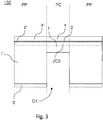
Dans un premier mode de réalisation illustré à la
De préférence, dans ce mode de réalisation, la partie périphérique PP comprend une troisième couche 3' d'un matériau conducteur ; une première couche 1' d'un matériau semi-conducteur recouvrant la troisième couche 3' et disposée en continuité de la première couche 1 de la partie centrale PC ; et une deuxième couche 2' d'un matériau conducteur recouvrant la première couche 1 et disposée en continuité de la deuxième couche 2 de la partie centrale PC.Preferably, in this embodiment, the peripheral part PP comprises a third layer 3 'of a conductive material; a
Dans cette configuration, appelée configuration Schottky, la zone de charge d'espace ZCE est formée par la diode Schottky constituée par la première couche 1 d'un matériau conducteur et la deuxième couche 2 d'un matériau semi-conducteur. La zone de charge d'espace ZCE se situe donc sur la partie centrale PC mais également sur la partie périphérique PP. En outre, la troisième couche 3' d'un matériau conducteur assure la collecte d'un premier type de porteurs de charge générés dans la zone de charge d'espace de charge ZCE tandis que la première couche 2,2' réalisée dans un matériau conducteur, assure la collecte d'un deuxième type de porteurs de charge générés dans la zone de charge d'espace ZCE. La deuxième couche 2,2' et la troisième couche 3,3' peuvent être constituées par un métal tel que le cuivre, le zinc ou l'or ou bien encore par du graphène mono ou multicouches. On peut également utiliser du nickel, de l'aluminium, du titane ou du tungstène. De manière plus générale, tout matériau conducteur adapté aux conditions de fabrication ou d'opération du dispositif peut être choisi. Le matériau utilisé pour la deuxième couche 2,2' peut être différent du matériau utilisé pour la troisième couche 3,3'. De préférence, les matériaux utilisés pour la troisième couche 3' peuvent être choisis de sorte à obtenir un contact ohmique entre la troisième couche 3' et la première couche 1' de la partie périphérique PP.In this configuration, called the Schottky configuration, the ZCE space charge zone is formed by the Schottky diode constituted by the
De préférence, le niveau de dopage de la première couche 1 de la partie centrale PC est identique au niveau de dopage de la première couche 1' de la partie périphérique. Le procédé de fabrication s'en trouve facilité car il ne nécessite qu'un seul niveau de dopage.Preferably, the doping level of the
De manière alternative, le niveau de dopage de la première couche 1 de la partie centrale PC est inférieur au niveau de dopage de la première couche 1' de la partie périphérique. Cette configuration permet de s'assurer une meilleure répartition du champ électrique et donc d'utiliser des tensions plus élevées pour la polarisation du détecteur.Alternatively, the doping level of the
Dans un exemple de réalisation, la première couche 1,1' a une épaisseur comprise entre 500 nm et 50 microns. Dans un mode de réalisation, la deuxième couche 2 ,2' a une épaisseur comprise entre 50nm et 200nm, de préférence sensiblement égale à 100nm.In an exemplary embodiment, the first layer 1.1 ′ has a thickness of between 500 nm and 50 microns. In one embodiment, the
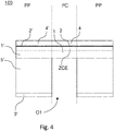
Dans un deuxième mode de réalisation d'un dispositif selon l'invention illustré à la
De préférence, dans ce mode de réalisation, la partie périphérique PP comprend une troisième couche 3' d'un matériau conducteur ; une première couche 1' d'un matériau semi-conducteur dopé dans un premier type de dopage recouvrant la troisième couche 3' et disposée en continuité de la première couche 1 de la partie centrale PC ; une deuxième couche 2' d'un matériau semi-conducteur dopé dans un deuxième type de dopage opposé au premier type de dopage recouvrant la première couche 1', la dite deuxième couche 2' étant disposée en continuité de la deuxième couche 2 de la partie centrale PC ; et une quatrième couche 4' d'un matériau conducteur, ladite quatrième couche 4' recouvrant la deuxième couche 2', la dite quatrième couche 4' étant disposée en continuité de la quatrième couche 4 de la partie PC. Dans un mode de réalisation, le dopage de la première couche 1,1' est de type n et le dopage de la deuxième couche 2,2' est de type p.Preferably, in this embodiment, the peripheral part PP comprises a third layer 3 'of a conductive material; a
Dans cette configuration, appelée configuration PN, la zone de charge d'espace ZCE est formée par la diode PN constituée par la première couche 1,1' d'un matériau semi-conducteur dopé dans un premier type de dopage et la deuxième couche 2,2' d'un matériau semi-conducteur dopé dans un deuxième type de dopage opposé au premier type de dopage. La zone d'espace de charge ZCE se situe donc sur la partie centrale PC mais également sur la partie périphérique PP. En outre, la troisième couche 3' de la partie périphérique assure la collecte d'un premier type de porteurs de charge générés dans la zone de charge d'espace ZCE tandis que la quatrième couche 4,4', réalisée dans un matériau conducteur, assure la collecte d'un deuxième type de porteurs de charge générés dans la zone de charge d'espace ZCE. La troisième couche 3' et la quatrième couche 4,4' peuvent être constituées par un métal tel que le cuivre, le zinc ou l'or ou bien encore par du graphène mono ou multicouches. On peut également utiliser du nickel, de l'aluminium, du titane ou du tungstène. De manière plus générale, tout matériau conducteur adapté aux conditions de fabrication ou d'opération du dispositif peut être choisi. Le matériau utilisé pour la troisième couche 3' peut être différent du matériau utilisé pour la quatrième couche 4,4'. De préférence, les matériaux utilisés pour la troisième couche 3' peuvent être choisis de sorte à obtenir un contact ohmique entre la troisième couche 3' et la première couche 1' de la partie périphérique PP. De même, les matériaux utilisés pour la quatrième couche 4,4' peuvent être choisis de sorte à obtenir un contact ohmique entre la quatrième couche 4,4' et la deuxième couche 2,2'.In this configuration, called PN configuration, the space load area ZCE is formed by the PN diode constituted by the
De préférence, le niveau de dopage de la première couche 1 de la partie centrale PC est identique au niveau de dopage de la première couche 1' de la partie périphérique PP. De même, le niveau de dopage de la deuxième couche 2 de la partie centrale PC est identique au niveau de dopage de la deuxième couche 2' de la partie périphérique. Comme expliqué précédemment, le procédé de fabrication s'en trouve facilité car il ne nécessite qu'un seul niveau de dopage.Preferably, the doping level of the
Dans un exemple de réalisation, le dopage de la première couche 1,1' est de type n et le dopage de la deuxième couche 2,2' est de type p. Le niveau de dopage de la première couche 1,1' est compris entre 5.1014 et 5.1019 atomes par cm3, de préférence sensiblement égal à 5.1015 atomes par cm3. Le niveau de dopage de la deuxième couche 2,2' est compris entre 1.1016 et 5.1019 atomes par cm3, de préférence sensiblement égal à 1.1019 atomes par cm3.In an exemplary embodiment, the doping of the
De manière alternative, le niveau de dopage de la première couche 1 de la partie centrale PC est inférieur au niveau de dopage de la première couche 1' de la partie périphérique. De même, le niveau de dopage de la deuxième couche 2 de la partie centrale PC est inférieur au niveau de dopage de la deuxième couche 2' de la partie périphérique. Comme expliqué précédemment, cette configuration permet de s'assurer d'une meilleure répartition du champ électrique, ce qui permet d'utiliser des tensions plus élevés pour la polarisation du détecteur.Alternatively, the doping level of the
Dans un troisième mode de réalisation illustré à la
La cinquième couche 5' de la partie périphérique PP peut par exemple être obtenu par la gravure de l'orifice O1 dans une couche d'un matériau semi-conducteur dopé dans un premier type de dopage ladite couche étant présente dans la partie centrale PC et la partie périphérique PP avant gravure et étant gravée dans toute son épaisseur afin de former l'orifice O1. La gravure peut être effectué par une technique sèche de type RIE ou bien encore une technique humide.The
De préférence, le dopage de la première couche 1,1' et de la cinquième couche 5' de la partie périphérique PP est de type n et le dopage de la deuxième couche 2,2' est de type p. Le niveau de dopage de la cinquième couche 5' est compris entre 1.1016 et 1.1019 atomes par cm3, de préférence sensiblement égal à 11018 atomes par cm3. Le niveau de dopage de la première couche 1,1' est compris entre 5.1014 et 5.1019 atomes par cm3, de préférence sensiblement égal à 5.1015 atomes par cm3. Le niveau de dopage de la deuxième couche 2,2' est compris entre 1.1016 et 5.1019 atomes par cm3, de préférence sensiblement égal à 1.1019 atomes par cm3.Preferably, the doping of the
Dans un exemple de réalisation, la première couche 1,1' a une épaisseur comprise entre 500 nm et 50 microns ; la deuxième couche 2 ,2' a une épaisseur comprise entre 50 et 200nm, de préférence sensiblement égale à 100nm ; et la cinquième couche a une épaisseur comprise entre 250 et 350 microns, de préférence sensiblement égale à 300 micron.In an exemplary embodiment, the first layer 1.1 ′ has a thickness of between 500 nm and 50 microns; the
Le faisceau à mesurer ne traversant le détecteur qu'au niveau de la partie centrale PC, il peut être avantageux de déporter la totalité des électrodes nécessaires à la récupération des porteurs de charge au niveau de la partie périphérique. Pour cela, dans un quatrième mode de réalisation illustré à la
Dans le mode de réalisation précédent, la zone de charge d'espace ZCE est présente à la fois dans la partie centrale PC et la partie périphérique PP du dispositif. Cependant, il peut être avantageux de n'avoir une zone de charge d'espace ZCE que dans la partie centrale PC du dispositif de détection. Pour cela, dans un cinquième mode de réalisation illustré à la
Dans ce mode de réalisation, la quatrième couche 4, 4' forme une marche entre la partie périphérique PP et la partie centrale PC couvrant une surface latérale de la sixième couche 6 de sorte à assurer une continuité entre la quatrième couche 4 de la partie centrale PC et la quatrième couche 4' de la partie périphérique PP. Dans ce mode de réalisation, la sixième couche 6' ne se trouve que sur la partie périphérique et forme donc un deuxième orifice 02.In this embodiment, the
Cependant, dans le mode de réalisation précédent, la quatrième couche 4' de la partie centrale PC recouvre l'intégralité de la partie centrale PC par laquelle passe le faisceau à mesurer. Il peut être avantageux dans certaines situations de diminuer ce phénomène d'absorption. A cette fin, dans un sixième mode de réalisation illustré à la
Par ailleurs, lorsque l'étendue de la deuxième couche 2,2' est limitée à la partie centrale PC, la structure MIS (Métal Isolant Semi-Conducteur) constituée au niveau de la partie périphérique PP du dispositif formé par la première couche de la partie périphérique 1', la sixième couche de la partie périphérique 6' et par la quatrième couche 4' de la partie périphérique peut venir perturber la mesure en induisant notamment des effets capacitifs. Afin de prévenir ce phénomène, dans un septième mode de réalisation illustré à la
Dans un huitième mode de réalisation illustré à la
Claims (14)
- Device (100) for measuring a particle beam including a first part, designated central part (PC), a second part, designated peripheral part (PP), a front face (F) and a rear face (B), the front face (F) being parallel to the rear face (B);- the central part (PC) comprising means for forming a space charge zone (ZCE) intended to be traversed by a particle beam (FS) to measure, charge carriers of a first type and of a second type being generated by said beam (FS) when the latter traverses the space charge zone (ZCE);- the peripheral part (PP) comprising means for collecting at least one type of charge carrier among the first type or the second type of charge carriers generated at the level of the space charge zone (ZCE);the peripheral part (PP) surrounding the central part (PC) such that a particle beam (FS) can traverse the central part (PC) without traversing the peripheral part (PP), the device for measuring being characterized in that it comprises an orifice (O1) being arranged at the level of the rear face (B), in a region of the central part (PC) such that the thickness of said region of the central part (PC) along an axis normal to the front face (F) is less than the thickness of the peripheral part (PP) along said normal axis.
- Measuring device (100) according to the preceding claim characterised in that at least one interface facing the orifice (O1) arranged in the rear (B) or front face is structured so as to favour the absorption, the transmission or the reflection of one or several wavelengths.
- Measuring device (100) according to one of the preceding claims characterised in that metal beads (BI) are present in the central part (PC), said beads (BI) being spread out according to a periodic structure so as to form a plasmonic array.
- Measuring device (100) according to one of the preceding claims characterised in that the central part (PC) is made of a wide gap semiconductor material.
- Measuring device (100) according to the preceding claim characterised in that the semiconductor is silicon carbide.
- Measuring device (100) according to one of the preceding claims characterised in that the space charge zone (ZCE) is formed by means of a Schottky diode, a PN diode or a PIN diode.
- Measuring device (100) according to one of the preceding claims characterised in that the space charge zone (ZCE) of the central part (PC) is uniquely situated in the region of the central part (PC) facing the orifice (O1).
- Measuring device (100) according to one of claims 1 to 4 characterised in that the space charge zone (ZCE) of the central part (PC) extends beyond the region of the central part (PC) facing the orifice (O1).
- Measuring device (100) according to one of claims 1 to 4 characterised in that the central part (PC) includes:- a first layer (1) of a semiconductor material;- a second layer (2) of a conductor material covering the first layer (1);the space charge zone (ZCE) being formed by the Schottky diode formed by the first layer (1) and the second layer (2), the orifice (O1) being arranged in the first layer (1).
- Measuring device (100) according to the preceding claim characterised in that the peripheral part (PP) includes:- a third layer (3') of a conductor material;- a first layer (1') of a semiconductor material covering the third layer (3') and arranged in continuity with the first layer (1) of the central part (PC);- a second layer (2') of a conductor material covering the first layer (1) and arranged in continuity with the second layer (2) of the central part (PC);the third layer (3') of a conductor material ensuring the collection of a first type of charge carrier generated in the space charge zone (ZCE).
- Measuring device (100) according to one of claims 1 to 4 characterised in that the central part (PC) includes:- a first layer (1) of a semiconductor material doped with a first type of doping;- a second layer (2) of a semiconductor material doped with a second type of doping opposite to the first type of doping, said second layer (2) covering the first layer (1);- a fourth layer (4) of a conductor material, said fourth layer (4) covering the second layer (2);the space charge zone (ZCE) being formed by the PN diode formed by the first layer (1) and the second layer (2), the orifice (O1) being arranged in the first layer (1).
- Measuring device (100) according to the preceding claim characterised in that the peripheral part includes:- a third layer (3') of a conductor material;- a first layer (1') of a semiconductor material doped with a first type of doping covering the third layer (3') and arranged in continuity with the first layer (1) of the central part (PC);- a second layer (2') of a semiconductor material doped with a second type of doping opposite to the first type of doping covering the first layer (1'), said second layer (2') being arranged in continuity with the second layer (2) of the central part (PC);- a fourth layer (4') of a conductor material, said fourth layer (4') covering the second layer (2'), said fourth layer (4') being arranged in continuity with the fourth layer (4) of the central part (PC);the third layer (3) of a conductor material ensuring the collection of a first type of charge carrier generated in the space charge zone (ZCE).
- Measuring device (100) according to claim 9 characterised in that the peripheral part (PP) includes:- a third layer (3') of a conductor material;- a first layer (1') of a semiconductor material doped with a first type of doping covering the third layer (3') and arranged in continuity with the first layer (1) of the central part (PC), the first layer (1) of the central part (PC) and of the peripheral part (PP) having the same doping level;- a sixth layer (6) of an oxide covering the first layer (1):- a fourth layer (4') of a conductor material covering the sixth layer (6);the fourth layer (4, 4') forming a step between the peripheral part (PP) and the central part (PC) covering a lateral surface of the sixth layer (6) so as to ensure continuity between the fourth layer (4) of the central part (PC) and the fourth layer (4') of the peripheral part (PP).
- Device according to one of the two preceding claims characterised in that the peripheral part (PP) comprises a fifth layer (5') of a semiconductor material doped with a first type of doping, the doping level of the fifth layer (5') being higher than the doping level of the first layer (1'), the fourth layer being situated between the third layer (3') and the first layer (1') of the peripheral part (PP).
Applications Claiming Priority (2)
| Application Number | Priority Date | Filing Date | Title |
|---|---|---|---|
| FR1654382A FR3051557A1 (en) | 2016-05-17 | 2016-05-17 | PARTICULATE DETECTOR PRODUCED IN SEMICONDUCTOR MATERIAL |
| PCT/EP2017/061637 WO2017198630A1 (en) | 2016-05-17 | 2017-05-15 | Particle detector made of a semiconductor material |
Publications (2)
| Publication Number | Publication Date |
|---|---|
| EP3458878A1 EP3458878A1 (en) | 2019-03-27 |
| EP3458878B1 true EP3458878B1 (en) | 2020-07-01 |
Family
ID=57184536
Family Applications (1)
| Application Number | Title | Priority Date | Filing Date |
|---|---|---|---|
| EP17723993.6A Active EP3458878B1 (en) | 2016-05-17 | 2017-05-15 | Particle detector made of a semiconductor material |
Country Status (6)
| Country | Link |
|---|---|
| US (1) | US10591620B2 (en) |
| EP (1) | EP3458878B1 (en) |
| CA (1) | CA3024395C (en) |
| DK (1) | DK3458878T3 (en) |
| FR (1) | FR3051557A1 (en) |
| WO (1) | WO2017198630A1 (en) |
Cited By (1)
| Publication number | Priority date | Publication date | Assignee | Title |
|---|---|---|---|---|
| FR3118300A1 (en) * | 2020-12-23 | 2022-06-24 | Université D'aix Marseille | PARTICLE DETECTOR COMPRISING A POROUS REGION MADE IN A SEMI-CONDUCTOR MATERIAL AND ASSOCIATED MANUFACTURING METHOD |
Families Citing this family (4)
| Publication number | Priority date | Publication date | Assignee | Title |
|---|---|---|---|---|
| FR3099293A1 (en) * | 2019-07-26 | 2021-01-29 | Université D'aix Marseille | One-piece semiconductor material particle detection device |
| FR3100343B1 (en) | 2019-09-02 | 2021-08-27 | Centre Nat Rech Scient | DOSIMETER |
| FR3112400B1 (en) | 2020-07-10 | 2022-06-17 | Univ Aix Marseille | Method for manufacturing an irradiation head of a target with a beam of ionizing particles |
| FR3119246B1 (en) | 2021-01-27 | 2023-02-24 | Centre Nat Rech Scient | METHOD FOR MANUFACTURING A FLOW DETECTOR OF A FIRST AND A SECOND IONIZING RADIATION |
Family Cites Families (7)
| Publication number | Priority date | Publication date | Assignee | Title |
|---|---|---|---|---|
| ES2036206T3 (en) * | 1986-04-11 | 1993-05-16 | American Telephone And Telegraph Company | DEVICE INCLUDING A RADIATION SENSOR. |
| EP0736780B1 (en) * | 1995-04-07 | 2002-07-24 | Rikagaku Kenkyusho | X-ray beam position monitor and its position measurement method |
| US7253434B2 (en) * | 2002-10-29 | 2007-08-07 | President And Fellows Of Harvard College | Suspended carbon nanotube field effect transistor |
| JP5096747B2 (en) * | 2006-03-02 | 2012-12-12 | 株式会社神戸製鋼所 | Beam detection member and beam detector using the same |
| US7586167B2 (en) * | 2006-05-05 | 2009-09-08 | Virgin Islands Microsystems, Inc. | Detecting plasmons using a metallurgical junction |
| US7816651B2 (en) * | 2007-09-27 | 2010-10-19 | Varian Medical Systems, Inc. | High detective quantum efficiency X-ray detectors |
| US9515211B2 (en) * | 2013-07-26 | 2016-12-06 | University Of South Carolina | Schottky barrier detection devices having a 4H-SiC n-type epitaxial layer |
-
2016
- 2016-05-17 FR FR1654382A patent/FR3051557A1/en active Pending
-
2017
- 2017-05-15 DK DK17723993.6T patent/DK3458878T3/en active
- 2017-05-15 EP EP17723993.6A patent/EP3458878B1/en active Active
- 2017-05-15 CA CA3024395A patent/CA3024395C/en active Active
- 2017-05-15 US US16/302,426 patent/US10591620B2/en active Active
- 2017-05-15 WO PCT/EP2017/061637 patent/WO2017198630A1/en unknown
Non-Patent Citations (1)
| Title |
|---|
| None * |
Cited By (2)
| Publication number | Priority date | Publication date | Assignee | Title |
|---|---|---|---|---|
| FR3118300A1 (en) * | 2020-12-23 | 2022-06-24 | Université D'aix Marseille | PARTICLE DETECTOR COMPRISING A POROUS REGION MADE IN A SEMI-CONDUCTOR MATERIAL AND ASSOCIATED MANUFACTURING METHOD |
| WO2022136516A1 (en) * | 2020-12-23 | 2022-06-30 | Université D'aix Marseille | Particle detector comprising a porous region made of a semi-conductor material, and associated manufacturing method |
Also Published As
| Publication number | Publication date |
|---|---|
| DK3458878T3 (en) | 2020-09-28 |
| US20190277983A1 (en) | 2019-09-12 |
| CA3024395A1 (en) | 2017-11-23 |
| WO2017198630A1 (en) | 2017-11-23 |
| EP3458878A1 (en) | 2019-03-27 |
| FR3051557A1 (en) | 2017-11-24 |
| CA3024395C (en) | 2024-03-26 |
| US10591620B2 (en) | 2020-03-17 |
Similar Documents
| Publication | Publication Date | Title |
|---|---|---|
| EP3458878B1 (en) | Particle detector made of a semiconductor material | |
| EP2752893B1 (en) | Avalanche-photodiode semiconductor structure and method for manufacturing such a structure | |
| EP2865017B1 (en) | Semiconductor structure with absorbing region in a focusing cavity | |
| FR2970599A1 (en) | PHOTODETECTOR OPTIMIZED BY METALLIC TEXTURATION AGENCED IN REAR FACING | |
| EP2339640A1 (en) | Photodetector with plasmon structure | |
| EP2786426B1 (en) | Semiconductor structure able to receive electromagnetic radiation, semiconductor component and process for fabricating such a semiconductor structure | |
| EP2937902B1 (en) | Cdhgte photodiode array | |
| WO2012080989A2 (en) | Photodetection device | |
| EP2750203B1 (en) | Avalanche-photodiode semiconductor structure with low response time and method for manufacturing such a photodiode | |
| EP2276072B1 (en) | Photodetector element | |
| EP2939275B1 (en) | Avalanche photodiode semiconductor structure having a high signal-to-noise ratio and method for manufacturing such a photodiode | |
| EP2432033A2 (en) | Multi-layer bispectral detector with photodiodes | |
| EP2801115B1 (en) | Photodetection device | |
| EP3703138B1 (en) | Structure for detecting electromagnetic radiation with high absorption efficiency and method for manufacturing such a structure | |
| EP3208854A1 (en) | Photodiode structure, component and manufacturing method of a photodiode structure | |
| WO2022136516A1 (en) | Particle detector comprising a porous region made of a semi-conductor material, and associated manufacturing method | |
| WO2013030482A1 (en) | Reflector device for rear face of optical devices | |
| EP2382672A1 (en) | Method for making a photodiode, and corresponding photodiode and electromagnetic radiation detector |
Legal Events
| Date | Code | Title | Description |
|---|---|---|---|
| STAA | Information on the status of an ep patent application or granted ep patent |
Free format text: STATUS: UNKNOWN |
|
| STAA | Information on the status of an ep patent application or granted ep patent |
Free format text: STATUS: THE INTERNATIONAL PUBLICATION HAS BEEN MADE |
|
| PUAI | Public reference made under article 153(3) epc to a published international application that has entered the european phase |
Free format text: ORIGINAL CODE: 0009012 |
|
| STAA | Information on the status of an ep patent application or granted ep patent |
Free format text: STATUS: REQUEST FOR EXAMINATION WAS MADE |
|
| 17P | Request for examination filed |
Effective date: 20181116 |
|
| AK | Designated contracting states |
Kind code of ref document: A1 Designated state(s): AL AT BE BG CH CY CZ DE DK EE ES FI FR GB GR HR HU IE IS IT LI LT LU LV MC MK MT NL NO PL PT RO RS SE SI SK SM TR |
|
| AX | Request for extension of the european patent |
Extension state: BA ME |
|
| DAV | Request for validation of the european patent (deleted) | ||
| DAX | Request for extension of the european patent (deleted) | ||
| GRAP | Despatch of communication of intention to grant a patent |
Free format text: ORIGINAL CODE: EPIDOSNIGR1 |
|
| STAA | Information on the status of an ep patent application or granted ep patent |
Free format text: STATUS: GRANT OF PATENT IS INTENDED |
|
| INTG | Intention to grant announced |
Effective date: 20191212 |
|
| RIN1 | Information on inventor provided before grant (corrected) |
Inventor name: OTTAVIANI, LAURENT Inventor name: VERVISCH, WILFRIED VIVIAN ROLAND Inventor name: BIONDO, STEPHANE Inventor name: HURTADO EP VERVISCH, VANESSA LAURENCE JILL |
|
| GRAS | Grant fee paid |
Free format text: ORIGINAL CODE: EPIDOSNIGR3 |
|
| GRAA | (expected) grant |
Free format text: ORIGINAL CODE: 0009210 |
|
| STAA | Information on the status of an ep patent application or granted ep patent |
Free format text: STATUS: THE PATENT HAS BEEN GRANTED |
|
| AK | Designated contracting states |
Kind code of ref document: B1 Designated state(s): AL AT BE BG CH CY CZ DE DK EE ES FI FR GB GR HR HU IE IS IT LI LT LU LV MC MK MT NL NO PL PT RO RS SE SI SK SM TR |
|
| REG | Reference to a national code |
Ref country code: CH Ref legal event code: EP Ref country code: AT Ref legal event code: REF Ref document number: 1286682 Country of ref document: AT Kind code of ref document: T Effective date: 20200715 |
|
| REG | Reference to a national code |
Ref country code: IE Ref legal event code: FG4D Free format text: LANGUAGE OF EP DOCUMENT: FRENCH |
|
| REG | Reference to a national code |
Ref country code: DE Ref legal event code: R096 Ref document number: 602017019032 Country of ref document: DE |
|
| REG | Reference to a national code |
Ref country code: DK Ref legal event code: T3 Effective date: 20200924 |
|
| REG | Reference to a national code |
Ref country code: NL Ref legal event code: FP |
|
| REG | Reference to a national code |
Ref country code: SE Ref legal event code: TRGR |
|
| REG | Reference to a national code |
Ref country code: CH Ref legal event code: NV Representative=s name: VALIPAT S.A. C/O BOVARD SA NEUCHATEL, CH |
|
| REG | Reference to a national code |
Ref country code: NO Ref legal event code: T2 Effective date: 20200701 |
|
| REG | Reference to a national code |
Ref country code: LT Ref legal event code: MG4D |
|
| PG25 | Lapsed in a contracting state [announced via postgrant information from national office to epo] |
Ref country code: BG Free format text: LAPSE BECAUSE OF FAILURE TO SUBMIT A TRANSLATION OF THE DESCRIPTION OR TO PAY THE FEE WITHIN THE PRESCRIBED TIME-LIMIT Effective date: 20201001 |
|
| PG25 | Lapsed in a contracting state [announced via postgrant information from national office to epo] |
Ref country code: ES Free format text: LAPSE BECAUSE OF FAILURE TO SUBMIT A TRANSLATION OF THE DESCRIPTION OR TO PAY THE FEE WITHIN THE PRESCRIBED TIME-LIMIT Effective date: 20200701 Ref country code: PT Free format text: LAPSE BECAUSE OF FAILURE TO SUBMIT A TRANSLATION OF THE DESCRIPTION OR TO PAY THE FEE WITHIN THE PRESCRIBED TIME-LIMIT Effective date: 20201102 Ref country code: CZ Free format text: LAPSE BECAUSE OF FAILURE TO SUBMIT A TRANSLATION OF THE DESCRIPTION OR TO PAY THE FEE WITHIN THE PRESCRIBED TIME-LIMIT Effective date: 20200701 Ref country code: LT Free format text: LAPSE BECAUSE OF FAILURE TO SUBMIT A TRANSLATION OF THE DESCRIPTION OR TO PAY THE FEE WITHIN THE PRESCRIBED TIME-LIMIT Effective date: 20200701 Ref country code: HR Free format text: LAPSE BECAUSE OF FAILURE TO SUBMIT A TRANSLATION OF THE DESCRIPTION OR TO PAY THE FEE WITHIN THE PRESCRIBED TIME-LIMIT Effective date: 20200701 Ref country code: GR Free format text: LAPSE BECAUSE OF FAILURE TO SUBMIT A TRANSLATION OF THE DESCRIPTION OR TO PAY THE FEE WITHIN THE PRESCRIBED TIME-LIMIT Effective date: 20201002 Ref country code: FI Free format text: LAPSE BECAUSE OF FAILURE TO SUBMIT A TRANSLATION OF THE DESCRIPTION OR TO PAY THE FEE WITHIN THE PRESCRIBED TIME-LIMIT Effective date: 20200701 |
|
| PG25 | Lapsed in a contracting state [announced via postgrant information from national office to epo] |
Ref country code: RS Free format text: LAPSE BECAUSE OF FAILURE TO SUBMIT A TRANSLATION OF THE DESCRIPTION OR TO PAY THE FEE WITHIN THE PRESCRIBED TIME-LIMIT Effective date: 20200701 Ref country code: PL Free format text: LAPSE BECAUSE OF FAILURE TO SUBMIT A TRANSLATION OF THE DESCRIPTION OR TO PAY THE FEE WITHIN THE PRESCRIBED TIME-LIMIT Effective date: 20200701 Ref country code: LV Free format text: LAPSE BECAUSE OF FAILURE TO SUBMIT A TRANSLATION OF THE DESCRIPTION OR TO PAY THE FEE WITHIN THE PRESCRIBED TIME-LIMIT Effective date: 20200701 Ref country code: IS Free format text: LAPSE BECAUSE OF FAILURE TO SUBMIT A TRANSLATION OF THE DESCRIPTION OR TO PAY THE FEE WITHIN THE PRESCRIBED TIME-LIMIT Effective date: 20201101 |
|
| REG | Reference to a national code |
Ref country code: DE Ref legal event code: R097 Ref document number: 602017019032 Country of ref document: DE |
|
| PG25 | Lapsed in a contracting state [announced via postgrant information from national office to epo] |
Ref country code: RO Free format text: LAPSE BECAUSE OF FAILURE TO SUBMIT A TRANSLATION OF THE DESCRIPTION OR TO PAY THE FEE WITHIN THE PRESCRIBED TIME-LIMIT Effective date: 20200701 Ref country code: SM Free format text: LAPSE BECAUSE OF FAILURE TO SUBMIT A TRANSLATION OF THE DESCRIPTION OR TO PAY THE FEE WITHIN THE PRESCRIBED TIME-LIMIT Effective date: 20200701 Ref country code: EE Free format text: LAPSE BECAUSE OF FAILURE TO SUBMIT A TRANSLATION OF THE DESCRIPTION OR TO PAY THE FEE WITHIN THE PRESCRIBED TIME-LIMIT Effective date: 20200701 |
|
| PLBE | No opposition filed within time limit |
Free format text: ORIGINAL CODE: 0009261 |
|
| STAA | Information on the status of an ep patent application or granted ep patent |
Free format text: STATUS: NO OPPOSITION FILED WITHIN TIME LIMIT |
|
| PG25 | Lapsed in a contracting state [announced via postgrant information from national office to epo] |
Ref country code: AL Free format text: LAPSE BECAUSE OF FAILURE TO SUBMIT A TRANSLATION OF THE DESCRIPTION OR TO PAY THE FEE WITHIN THE PRESCRIBED TIME-LIMIT Effective date: 20200701 |
|
| 26N | No opposition filed |
Effective date: 20210406 |
|
| PG25 | Lapsed in a contracting state [announced via postgrant information from national office to epo] |
Ref country code: SK Free format text: LAPSE BECAUSE OF FAILURE TO SUBMIT A TRANSLATION OF THE DESCRIPTION OR TO PAY THE FEE WITHIN THE PRESCRIBED TIME-LIMIT Effective date: 20200701 |
|
| PG25 | Lapsed in a contracting state [announced via postgrant information from national office to epo] |
Ref country code: SI Free format text: LAPSE BECAUSE OF FAILURE TO SUBMIT A TRANSLATION OF THE DESCRIPTION OR TO PAY THE FEE WITHIN THE PRESCRIBED TIME-LIMIT Effective date: 20200701 |
|
| PG25 | Lapsed in a contracting state [announced via postgrant information from national office to epo] |
Ref country code: LU Free format text: LAPSE BECAUSE OF NON-PAYMENT OF DUE FEES Effective date: 20210515 Ref country code: MC Free format text: LAPSE BECAUSE OF FAILURE TO SUBMIT A TRANSLATION OF THE DESCRIPTION OR TO PAY THE FEE WITHIN THE PRESCRIBED TIME-LIMIT Effective date: 20200701 |
|
| PG25 | Lapsed in a contracting state [announced via postgrant information from national office to epo] |
Ref country code: IE Free format text: LAPSE BECAUSE OF NON-PAYMENT OF DUE FEES Effective date: 20210515 |
|
| PG25 | Lapsed in a contracting state [announced via postgrant information from national office to epo] |
Ref country code: CY Free format text: LAPSE BECAUSE OF FAILURE TO SUBMIT A TRANSLATION OF THE DESCRIPTION OR TO PAY THE FEE WITHIN THE PRESCRIBED TIME-LIMIT Effective date: 20200701 |
|
| P01 | Opt-out of the competence of the unified patent court (upc) registered |
Effective date: 20230530 |
|
| REG | Reference to a national code |
Ref country code: AT Ref legal event code: UEP Ref document number: 1286682 Country of ref document: AT Kind code of ref document: T Effective date: 20200701 |
|
| PG25 | Lapsed in a contracting state [announced via postgrant information from national office to epo] |
Ref country code: HU Free format text: LAPSE BECAUSE OF FAILURE TO SUBMIT A TRANSLATION OF THE DESCRIPTION OR TO PAY THE FEE WITHIN THE PRESCRIBED TIME-LIMIT; INVALID AB INITIO Effective date: 20170515 |
|
| PGFP | Annual fee paid to national office [announced via postgrant information from national office to epo] |
Ref country code: NO Payment date: 20230526 Year of fee payment: 7 Ref country code: NL Payment date: 20230530 Year of fee payment: 7 Ref country code: IT Payment date: 20230526 Year of fee payment: 7 Ref country code: FR Payment date: 20230530 Year of fee payment: 7 Ref country code: DK Payment date: 20230526 Year of fee payment: 7 Ref country code: DE Payment date: 20230526 Year of fee payment: 7 Ref country code: CH Payment date: 20230605 Year of fee payment: 7 |
|
| PGFP | Annual fee paid to national office [announced via postgrant information from national office to epo] |
Ref country code: SE Payment date: 20230526 Year of fee payment: 7 Ref country code: AT Payment date: 20230526 Year of fee payment: 7 |
|
| PGFP | Annual fee paid to national office [announced via postgrant information from national office to epo] |
Ref country code: BE Payment date: 20230530 Year of fee payment: 7 |
|
| PGFP | Annual fee paid to national office [announced via postgrant information from national office to epo] |
Ref country code: GB Payment date: 20230530 Year of fee payment: 7 |