EP2865017B1 - Semiconductor structure with absorbing region in a focusing cavity - Google Patents
Semiconductor structure with absorbing region in a focusing cavity Download PDFInfo
- Publication number
- EP2865017B1 EP2865017B1 EP13729748.7A EP13729748A EP2865017B1 EP 2865017 B1 EP2865017 B1 EP 2865017B1 EP 13729748 A EP13729748 A EP 13729748A EP 2865017 B1 EP2865017 B1 EP 2865017B1
- Authority
- EP
- European Patent Office
- Prior art keywords
- semiconducting
- mesa
- area
- layer
- contact
- Prior art date
- Legal status (The legal status is an assumption and is not a legal conclusion. Google has not performed a legal analysis and makes no representation as to the accuracy of the status listed.)
- Active
Links
- 239000004065 semiconductor Substances 0.000 title claims description 288
- 230000005670 electromagnetic radiation Effects 0.000 claims description 77
- 239000000463 material Substances 0.000 claims description 37
- 239000000969 carrier Substances 0.000 claims description 27
- 238000004519 manufacturing process Methods 0.000 claims description 20
- 229910052793 cadmium Inorganic materials 0.000 claims description 17
- BDOSMKKIYDKNTQ-UHFFFAOYSA-N cadmium atom Chemical compound [Cd] BDOSMKKIYDKNTQ-UHFFFAOYSA-N 0.000 claims description 17
- 238000005530 etching Methods 0.000 claims description 13
- 230000003287 optical effect Effects 0.000 claims description 13
- 230000005855 radiation Effects 0.000 claims description 9
- 239000000758 substrate Substances 0.000 claims description 6
- 238000000151 deposition Methods 0.000 claims description 5
- QSHDDOUJBYECFT-UHFFFAOYSA-N mercury Chemical compound [Hg] QSHDDOUJBYECFT-UHFFFAOYSA-N 0.000 claims description 5
- 229910052753 mercury Inorganic materials 0.000 claims description 5
- 238000000034 method Methods 0.000 claims description 4
- 239000012535 impurity Substances 0.000 claims description 3
- 229910052714 tellurium Inorganic materials 0.000 claims description 3
- PORWMNRCUJJQNO-UHFFFAOYSA-N tellurium atom Chemical compound [Te] PORWMNRCUJJQNO-UHFFFAOYSA-N 0.000 claims description 3
- 230000003247 decreasing effect Effects 0.000 claims description 2
- 230000005693 optoelectronics Effects 0.000 description 12
- 239000005083 Zinc sulfide Substances 0.000 description 6
- 239000012141 concentrate Substances 0.000 description 6
- 238000005259 measurement Methods 0.000 description 6
- 239000004020 conductor Substances 0.000 description 5
- 238000001514 detection method Methods 0.000 description 5
- 239000011810 insulating material Substances 0.000 description 5
- JBRZTFJDHDCESZ-UHFFFAOYSA-N AsGa Chemical compound [As]#[Ga] JBRZTFJDHDCESZ-UHFFFAOYSA-N 0.000 description 4
- GPXJNWSHGFTCBW-UHFFFAOYSA-N Indium phosphide Chemical compound [In]#P GPXJNWSHGFTCBW-UHFFFAOYSA-N 0.000 description 4
- 229910000661 Mercury cadmium telluride Inorganic materials 0.000 description 4
- 229910052581 Si3N4 Inorganic materials 0.000 description 4
- VYPSYNLAJGMNEJ-UHFFFAOYSA-N Silicium dioxide Chemical compound O=[Si]=O VYPSYNLAJGMNEJ-UHFFFAOYSA-N 0.000 description 4
- MCMSPRNYOJJPIZ-UHFFFAOYSA-N cadmium;mercury;tellurium Chemical compound [Cd]=[Te]=[Hg] MCMSPRNYOJJPIZ-UHFFFAOYSA-N 0.000 description 4
- 238000009792 diffusion process Methods 0.000 description 4
- 230000005672 electromagnetic field Effects 0.000 description 4
- 239000010931 gold Substances 0.000 description 4
- 230000009467 reduction Effects 0.000 description 4
- HQVNEWCFYHHQES-UHFFFAOYSA-N silicon nitride Chemical compound N12[Si]34N5[Si]62N3[Si]51N64 HQVNEWCFYHHQES-UHFFFAOYSA-N 0.000 description 4
- 238000010521 absorption reaction Methods 0.000 description 3
- 230000015572 biosynthetic process Effects 0.000 description 3
- 230000007423 decrease Effects 0.000 description 3
- 238000004377 microelectronic Methods 0.000 description 3
- DRDVZXDWVBGGMH-UHFFFAOYSA-N zinc;sulfide Chemical compound [S-2].[Zn+2] DRDVZXDWVBGGMH-UHFFFAOYSA-N 0.000 description 3
- 229910004613 CdTe Inorganic materials 0.000 description 2
- 229910004298 SiO 2 Inorganic materials 0.000 description 2
- 230000006978 adaptation Effects 0.000 description 2
- 230000008901 benefit Effects 0.000 description 2
- 230000008859 change Effects 0.000 description 2
- 239000011651 chromium Substances 0.000 description 2
- 238000010586 diagram Methods 0.000 description 2
- 238000005516 engineering process Methods 0.000 description 2
- PCHJSUWPFVWCPO-UHFFFAOYSA-N gold Chemical compound [Au] PCHJSUWPFVWCPO-UHFFFAOYSA-N 0.000 description 2
- 229910052737 gold Inorganic materials 0.000 description 2
- 238000009396 hybridization Methods 0.000 description 2
- 230000006872 improvement Effects 0.000 description 2
- 229910052738 indium Inorganic materials 0.000 description 2
- APFVFJFRJDLVQX-UHFFFAOYSA-N indium atom Chemical compound [In] APFVFJFRJDLVQX-UHFFFAOYSA-N 0.000 description 2
- 230000010287 polarization Effects 0.000 description 2
- 238000005215 recombination Methods 0.000 description 2
- 230000006798 recombination Effects 0.000 description 2
- 230000035945 sensitivity Effects 0.000 description 2
- 235000012239 silicon dioxide Nutrition 0.000 description 2
- 239000000377 silicon dioxide Substances 0.000 description 2
- 239000010936 titanium Substances 0.000 description 2
- 230000007704 transition Effects 0.000 description 2
- MARUHZGHZWCEQU-UHFFFAOYSA-N 5-phenyl-2h-tetrazole Chemical compound C1=CC=CC=C1C1=NNN=N1 MARUHZGHZWCEQU-UHFFFAOYSA-N 0.000 description 1
- VYZAMTAEIAYCRO-UHFFFAOYSA-N Chromium Chemical compound [Cr] VYZAMTAEIAYCRO-UHFFFAOYSA-N 0.000 description 1
- 241001080024 Telles Species 0.000 description 1
- RTAQQCXQSZGOHL-UHFFFAOYSA-N Titanium Chemical compound [Ti] RTAQQCXQSZGOHL-UHFFFAOYSA-N 0.000 description 1
- 239000011324 bead Substances 0.000 description 1
- QWUZMTJBRUASOW-UHFFFAOYSA-N cadmium tellanylidenezinc Chemical compound [Zn].[Cd].[Te] QWUZMTJBRUASOW-UHFFFAOYSA-N 0.000 description 1
- 229910052804 chromium Inorganic materials 0.000 description 1
- 230000008021 deposition Effects 0.000 description 1
- 239000006185 dispersion Substances 0.000 description 1
- 238000009826 distribution Methods 0.000 description 1
- 230000000694 effects Effects 0.000 description 1
- 230000005684 electric field Effects 0.000 description 1
- 238000010292 electrical insulation Methods 0.000 description 1
- 230000005764 inhibitory process Effects 0.000 description 1
- 230000007246 mechanism Effects 0.000 description 1
- -1 mercury-cadmium tellurides Chemical class 0.000 description 1
- 229910052751 metal Inorganic materials 0.000 description 1
- 239000002184 metal Substances 0.000 description 1
- 230000004048 modification Effects 0.000 description 1
- 238000012986 modification Methods 0.000 description 1
- 230000000737 periodic effect Effects 0.000 description 1
- 230000004044 response Effects 0.000 description 1
- 230000002441 reversible effect Effects 0.000 description 1
- 229910052594 sapphire Inorganic materials 0.000 description 1
- 239000010980 sapphire Substances 0.000 description 1
- 238000000926 separation method Methods 0.000 description 1
- 229910052710 silicon Inorganic materials 0.000 description 1
- 239000010703 silicon Substances 0.000 description 1
- HBMJWWWQQXIZIP-UHFFFAOYSA-N silicon carbide Chemical compound [Si+]#[C-] HBMJWWWQQXIZIP-UHFFFAOYSA-N 0.000 description 1
- 229910010271 silicon carbide Inorganic materials 0.000 description 1
- 229910052715 tantalum Inorganic materials 0.000 description 1
- GUVRBAGPIYLISA-UHFFFAOYSA-N tantalum atom Chemical compound [Ta] GUVRBAGPIYLISA-UHFFFAOYSA-N 0.000 description 1
- 229910052719 titanium Inorganic materials 0.000 description 1
- 230000001131 transforming effect Effects 0.000 description 1
Images


Classifications
-
- H—ELECTRICITY
- H01—ELECTRIC ELEMENTS
- H01L—SEMICONDUCTOR DEVICES NOT COVERED BY CLASS H10
- H01L31/00—Semiconductor devices sensitive to infrared radiation, light, electromagnetic radiation of shorter wavelength or corpuscular radiation and specially adapted either for the conversion of the energy of such radiation into electrical energy or for the control of electrical energy by such radiation; Processes or apparatus specially adapted for the manufacture or treatment thereof or of parts thereof; Details thereof
- H01L31/02—Details
- H01L31/0232—Optical elements or arrangements associated with the device
- H01L31/02327—Optical elements or arrangements associated with the device the optical elements being integrated or being directly associated to the device, e.g. back reflectors
-
- H—ELECTRICITY
- H01—ELECTRIC ELEMENTS
- H01L—SEMICONDUCTOR DEVICES NOT COVERED BY CLASS H10
- H01L31/00—Semiconductor devices sensitive to infrared radiation, light, electromagnetic radiation of shorter wavelength or corpuscular radiation and specially adapted either for the conversion of the energy of such radiation into electrical energy or for the control of electrical energy by such radiation; Processes or apparatus specially adapted for the manufacture or treatment thereof or of parts thereof; Details thereof
- H01L31/08—Semiconductor devices sensitive to infrared radiation, light, electromagnetic radiation of shorter wavelength or corpuscular radiation and specially adapted either for the conversion of the energy of such radiation into electrical energy or for the control of electrical energy by such radiation; Processes or apparatus specially adapted for the manufacture or treatment thereof or of parts thereof; Details thereof in which radiation controls flow of current through the device, e.g. photoresistors
- H01L31/10—Semiconductor devices sensitive to infrared radiation, light, electromagnetic radiation of shorter wavelength or corpuscular radiation and specially adapted either for the conversion of the energy of such radiation into electrical energy or for the control of electrical energy by such radiation; Processes or apparatus specially adapted for the manufacture or treatment thereof or of parts thereof; Details thereof in which radiation controls flow of current through the device, e.g. photoresistors characterised by at least one potential-jump barrier or surface barrier, e.g. phototransistors
- H01L31/101—Devices sensitive to infrared, visible or ultraviolet radiation
- H01L31/102—Devices sensitive to infrared, visible or ultraviolet radiation characterised by only one potential barrier or surface barrier
- H01L31/103—Devices sensitive to infrared, visible or ultraviolet radiation characterised by only one potential barrier or surface barrier the potential barrier being of the PN homojunction type
- H01L31/1032—Devices sensitive to infrared, visible or ultraviolet radiation characterised by only one potential barrier or surface barrier the potential barrier being of the PN homojunction type the devices comprising active layers formed only by AIIBVI compounds, e.g. HgCdTe IR photodiodes
-
- H—ELECTRICITY
- H01—ELECTRIC ELEMENTS
- H01L—SEMICONDUCTOR DEVICES NOT COVERED BY CLASS H10
- H01L31/00—Semiconductor devices sensitive to infrared radiation, light, electromagnetic radiation of shorter wavelength or corpuscular radiation and specially adapted either for the conversion of the energy of such radiation into electrical energy or for the control of electrical energy by such radiation; Processes or apparatus specially adapted for the manufacture or treatment thereof or of parts thereof; Details thereof
- H01L31/08—Semiconductor devices sensitive to infrared radiation, light, electromagnetic radiation of shorter wavelength or corpuscular radiation and specially adapted either for the conversion of the energy of such radiation into electrical energy or for the control of electrical energy by such radiation; Processes or apparatus specially adapted for the manufacture or treatment thereof or of parts thereof; Details thereof in which radiation controls flow of current through the device, e.g. photoresistors
- H01L31/10—Semiconductor devices sensitive to infrared radiation, light, electromagnetic radiation of shorter wavelength or corpuscular radiation and specially adapted either for the conversion of the energy of such radiation into electrical energy or for the control of electrical energy by such radiation; Processes or apparatus specially adapted for the manufacture or treatment thereof or of parts thereof; Details thereof in which radiation controls flow of current through the device, e.g. photoresistors characterised by at least one potential-jump barrier or surface barrier, e.g. phototransistors
- H01L31/101—Devices sensitive to infrared, visible or ultraviolet radiation
- H01L31/102—Devices sensitive to infrared, visible or ultraviolet radiation characterised by only one potential barrier or surface barrier
- H01L31/103—Devices sensitive to infrared, visible or ultraviolet radiation characterised by only one potential barrier or surface barrier the potential barrier being of the PN homojunction type
- H01L31/1035—Devices sensitive to infrared, visible or ultraviolet radiation characterised by only one potential barrier or surface barrier the potential barrier being of the PN homojunction type the devices comprising active layers formed only by AIIIBV compounds
-
- H—ELECTRICITY
- H01—ELECTRIC ELEMENTS
- H01L—SEMICONDUCTOR DEVICES NOT COVERED BY CLASS H10
- H01L31/00—Semiconductor devices sensitive to infrared radiation, light, electromagnetic radiation of shorter wavelength or corpuscular radiation and specially adapted either for the conversion of the energy of such radiation into electrical energy or for the control of electrical energy by such radiation; Processes or apparatus specially adapted for the manufacture or treatment thereof or of parts thereof; Details thereof
- H01L31/08—Semiconductor devices sensitive to infrared radiation, light, electromagnetic radiation of shorter wavelength or corpuscular radiation and specially adapted either for the conversion of the energy of such radiation into electrical energy or for the control of electrical energy by such radiation; Processes or apparatus specially adapted for the manufacture or treatment thereof or of parts thereof; Details thereof in which radiation controls flow of current through the device, e.g. photoresistors
- H01L31/10—Semiconductor devices sensitive to infrared radiation, light, electromagnetic radiation of shorter wavelength or corpuscular radiation and specially adapted either for the conversion of the energy of such radiation into electrical energy or for the control of electrical energy by such radiation; Processes or apparatus specially adapted for the manufacture or treatment thereof or of parts thereof; Details thereof in which radiation controls flow of current through the device, e.g. photoresistors characterised by at least one potential-jump barrier or surface barrier, e.g. phototransistors
- H01L31/101—Devices sensitive to infrared, visible or ultraviolet radiation
- H01L31/102—Devices sensitive to infrared, visible or ultraviolet radiation characterised by only one potential barrier or surface barrier
- H01L31/109—Devices sensitive to infrared, visible or ultraviolet radiation characterised by only one potential barrier or surface barrier the potential barrier being of the PN heterojunction type
-
- H—ELECTRICITY
- H01—ELECTRIC ELEMENTS
- H01L—SEMICONDUCTOR DEVICES NOT COVERED BY CLASS H10
- H01L31/00—Semiconductor devices sensitive to infrared radiation, light, electromagnetic radiation of shorter wavelength or corpuscular radiation and specially adapted either for the conversion of the energy of such radiation into electrical energy or for the control of electrical energy by such radiation; Processes or apparatus specially adapted for the manufacture or treatment thereof or of parts thereof; Details thereof
- H01L31/18—Processes or apparatus specially adapted for the manufacture or treatment of these devices or of parts thereof
Definitions
- the invention relates to the field of the detection and / or measurement of electromagnetic radiation and devices for such detection and / or measurement.
- These devices generally implement semiconductor structures capable of receiving electromagnetic radiation and transforming it into an electrical signal.
- the invention relates more particularly to a semiconductor structure, a semiconductor component and a method of manufacturing such a semiconductor structure.
- Semiconductor structures adapted to receive electromagnetic radiation generally comprise a first and a second semiconductor region in contact with each other and having respectively a first and a second conductivity type opposite to each other. In this way the first and the second zone together form, at their contact, a semiconductor junction.
- direct gap semiconductor material a semiconductor material whose maximum energy of the valence band and the minimum of energy of the conduction band are at a substantially equal value of the wave vector k in the FIG. energy dispersion of said semiconductor material.
- the structure can receive electromagnetic radiation over a large area without requiring an active area occupying a large volume.
- Such a concentration of the electromagnetic radiation can be obtained in particular, as described in the document EP 2276072 by means of a Fabry-Perot type concentrator which makes it possible to concentrate the electromagnetic radiation in a reduced area of the structure in which the junction can be arranged.
- the junction is arranged in the semiconductor layer at which the Fabry-Perot concentrator concentrates the electromagnetic radiation.
- the thickness of the structure on which the electromagnetic radiation is captured is limited by the semiconductor layer in which the junction is arranged. Since this layer must have a thickness between ⁇ 0 / 4n e and ⁇ 0 / 10n e , the thickness of the active zone of the junction on which the electromagnetic radiation is absorbed is therefore reduced and a part of the electromagnetic radiation can, because of this low thickness cross the structure without being absorbed.
- the present invention aims to remedy this disadvantage.
- An object of the invention is to provide a semiconductor structure which has an optimized signal-to-noise ratio with respect to the structures of the prior art.
- the relatively low concentration of majority carriers of the portion of the second semiconductor zone induces a depletion of the majority carriers in this same portion of the second semiconductor zone, thus limiting the risks of electron-hole pair recombinations which is the source of the current. darkness.
- the induced curvature of the strip along the portion of the second semiconducting zone allows a collection of photogenerated minority carriers by flow of the latter along the portion and not by diffusion. .
- the collection time is reduced compared to a structure collecting the photogenerated current by carrier diffusion.
- the response of the structure is thus reliable with respect to the structures of the prior art which have a greater probability of recombination of the photogenerated electron-hole pairs before their collection.
- a structure according to the invention allows a reproducible calibration with increased sensitivity to a structure according to the prior art.
- a cavity comprised in an optoelectronic component may be a resonant or optical cavity, such as a Fabry-Perot type cavity.
- a cavity is not necessarily empty since it may contain, for example, an active medium as is the case for a component of the semiconductor laser type.
- focusing is meant, in the field of optics and optoelectronics, the fact of converging a light beam so as to concentrate it in a small volume.
- portion essentially formed in the cavity is meant that the portion is at least partly disposed in the cavity, the portion of the second semiconductor zone having more than half of its volume in the first cavity.
- the portion of the second semiconductor zone represents most of the second semiconductor zone which is formed in the first cavity.
- the first cavity is a Fabry-Perot type cavity particularly adapted to allow a concentration of an electromagnetic field.
- the first cavity has, in at least one confinement direction, a dimension mean substantially equal to ⁇ 0 / 2n eff with n eff the average effective index in the second semiconductor zone.
- a Fabry-Perot cavity whose average dimension is substantially equal to ⁇ 0 / 2n eff is particularly suitable for concentrating an electromagnetic radiation whose wavelength is within the operating range.
- the confinement direction may be substantially perpendicular to the average reception direction.
- Such an orientation of the confinement dimension makes it possible to obtain a confinement of the structure in a perpendicular direction of the junction allowing the dimensioning, if necessary, of the thickness according to which the portion extends, thus limiting the part of the electromagnetic radiation which does not would not be absorbed during his passage in the structure.
- the dimension of the first cavity in the direction of confinement is a variable dimension, said dimension preferably decreasing from the first semiconductor zone to the second semiconductor zone.
- Such a variable dimension makes it possible to widen the range of wavelengths of the electromagnetic radiation which is focused in the first cavity.
- the dimension of the first cavity in the confinement direction varies substantially monotonously in the direction from the first semiconductor zone to the second semiconductor zone.
- the dimension of the first cavity in the direction of confinement varies at an angle between 0 and 40 ° with respect to the direction from the first semiconductor zone to the second semiconductor zone.
- the junction can be a heterojunction.
- Such a type of junction makes it possible to adapt the bandgap width of each semiconductor zone and can make it possible to optimize the portion of the electromagnetic radiation absorbed by the semiconductor functional zone of the junction.
- the first and second semiconducting zone may have bandgap widths of different energies, the second semiconductor zone may have an average energy gap bandwidth greater than that of a radiation whose wavelength is within the operating range.
- the electromagnetic radiation in a configuration in which the electromagnetic radiation passes through the first semiconductor zone before arriving in the second semiconductor zone, has a reduced attenuation as it passes through the first semiconductor zone.
- the first and the second semiconductor zone may have bandgap widths of different energies, the first semiconductor zone having a mean energy band gap width smaller than that of a radiation whose wavelength is within operating range.
- the second semiconductor zone is particularly suitable for the absorption of electromagnetic radiation.
- the second semiconductor zone comprises, in addition to said portion, a non-sparse portion in the cavity and having a mean energy band gap width greater than that of electromagnetic radiation whose wavelength is within the operating range, and said portion having an average energy gap bandwidth less than that of a electromagnetic radiation whose wavelength is within the first operating range.
- the first semiconductor zone may have a band gap that decreases towards the second semiconductor zone.
- the electromagnetic radiation is received in a medium of optical index n i , said incident index, the ratio between the effective index and the incident index n eff / n i being greater than 1, preferably substantially greater than 1.5, and still more preferably greater than 2.
- the optical index of a medium means the refractive index of the medium for the first range of wavelengths.
- the incident index medium n i may be a support of the structure.
- the incident index medium n i may be an air zone through which the radiation is received by the structure.
- the first and second semiconductor zones can be produced in semiconductor materials composed essentially of at least three same elements whose concentration in at least one of these elements makes it possible to vary the forbidden band width, said elements being preferably cadmium (Cd), mercury (Hg) and tellurium (Te).
- Such elements allow, by varying the concentration of at least one of these elements, the modification of the band gap along the structure thus giving access to the possibility of optimizing this bandgap according to the zones semiconductors of the structure and their function.
- mercury-cadmium tellurides have among other advantages to present a band gap that varies with the concentration in cadmium this without affecting their direct gap semiconductor property.
- Te tellurium
- Cd cadmium
- Hg mercury
- the operating range may be in the infrared wavelength range.
- Such a structure is particularly adapted to the manufacturing constraints of optoelectronics.
- a second semiconductor layer in contact with the surface of the first face which is opposite the first face, the mesa being in direct contact with the second semiconductor layer and in contact with the first semiconductor layer through the second layer semiconductor, the second layer having at least one portion whose concentration of majority carriers is ten times lower than that of the first semiconductor layer, the second semiconductor layer and the mesa forming the second semiconductor zone and the respective parts of the mesa and the second layer. semiconductor forming the portion of the second semiconductor zone.
- the mesa may be in direct contact with the first semiconductor layer.
- the fourth semiconductor zone has a second portion whose concentration in majority carriers is at least 10 times lower than the majority carrier concentration of the third semiconductor zone, said second portion being the portion of the fourth semiconductor zone which is in contact with the third semiconductor zone, the fourth semiconductor zone is essentially formed in a second cavity, said second cavity being adapted to concentrate in the second cavity part of the electromagnetic radiation which is received by the structure and whose wavelength is within a range of length waveforms said second operating range.
- Such third and fourth semiconductor zones and the second cavity associated therewith allow to increase the surface of the structure on which the electromagnetic radiation is collected and therefore the signal provided by the structure when the latter receives electromagnetic radiation.
- the second operating range is substantially the same as the first operating range.
- the structure has, for electromagnetic radiation whose wavelength is in the first operating range, a receiving surface of these electromagnetic radiations which is increased relative to a structure not comprising a second cavity adapted to focus. in the second cavity a portion of the electromagnetic radiation which is received by the structure and whose wavelength is in the first operating range.
- the second operating range may be different from the first operating range, the first and second operating range being preferably selected to cover a continuous wavelength range.
- the structure is adapted for the reception of electromagnetic radiation over a wavelength range of greater width than a structure having no second cavity.
- the invention also relates to a semiconductor component comprising a plurality of semiconductor structures for receiving electromagnetic radiation, at least one of the structures being a structure according to the invention.
- Such a component has, for the structure or structures according to the invention, a signal-to-noise ratio optimized vis-à-vis a component comprising only structures according to the prior art.
- Such a method allows the formation of a structure having in the operating range an improved signal-to-noise ratio with respect to a structure of the prior art.
- the manufacturing method may comprise between the step of forming the first semiconductor layer and the step of forming the mesa, a step of forming a second semiconductor layer of the second conductivity type in contact with the first semiconductor layer on the face of the first semiconductor layer opposite to the support, the mesa being formed in contact with the second semiconductor layer.
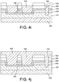
- the figure 1 illustrates a semiconductor structure, for receiving electromagnetic radiation 2 in a first wavelength range, according to a first embodiment of the invention.
- the first range of wavelengths which is called the operating range, is centered around a wavelength ⁇ 0 .
- the first operating range is a range of wavelengths that can be included in the wavelength range of visible, ultraviolet or infrared.
- the range of wavelengths is in the infrared range and may be, as required, a range of wavelengths of near infrared, mid-infrared or far-infrared.
- the semiconductor medium 100 is a support conventionally used for optoelectronic applications.
- the support is preferably a transparent substrate in the first operating range.
- the support 100 is made of a semiconductor material conventionally used for the applications of optoelectronics, such as, for example, silicon, silicon carbide, sapphire.
- the support has an optical index, or refractive index, n i .
- the support 100 is a cadmium zinc telluride substrate (CdZnTe) which is transparent in the wavelength range of the infrared.
- CdZnTe cadmium zinc telluride substrate
- the support is preferably at least partially insulating.
- the optical index n i of the support is 2.7.
- the support 100 is a substantially plane support whose first face is in contact with the first semiconductor layer 121.
- the second face of the support 100 is the face of the structure which, as illustrated on FIG. figure 1 , receives the electromagnetic radiation.
- the first semiconductor layer 121 is a semiconductor layer suitable for optoelectronic applications.
- the first semiconductor layer 121 is made of a direct gap semiconductor material such as gallium arsenide (GaAs) and indium phosphide (InP).
- the first semiconductor layer 121 has the first type of conductivity.
- the first type of conductivity is a conductivity type selected from the group comprising the type of conductivity whose majority carriers are the electrons and the type of conductivity whose majority carriers are the holes.
- the majority carrier concentration of the first semiconductor layer 121 is significantly important. It thus has good conductivity.
- the first semiconductor layer 121 may have, for example, a majority carrier concentration greater than 10 17 cm -3 .
- the forbidden band width of the first semiconductor layer 121 is preferably of a higher energy than that of an electromagnetic radiation whose wavelength is within the operating range.
- the bandgap width of the first semiconductor layer 121 may be variable or constant along its thickness. In the case where the forbidden band width of the first semiconductor layer 121 is variable along its thickness, the first semiconductor layer 121 has a band gap that decreases towards the second semiconductor layer 122. The decrease in width prohibited along the thickness of the first semiconductor layer 121 may be continuous or stepwise.
- the first semiconductor layer 121 is a mercury-cadmium telluride layer of the Cd X Hg 1-X Te type with X the cadmium content which is between 0.2 and 1.
- the minimum value of the proportion of cadmium X is chosen according to the operating range so that the first semiconductor layer 121 has a band gap whose energy is greater than that of electromagnetic radiation whose wavelength is between in the operating range.
- the minimum proportion of cadmium X may be greater than 0.5, and for the average infrared range of less than 5 ⁇ m, the proportion of cadmium X may be greater than 0.4.
- the minimum proportion of cadmium X may be greater than 0.3.
- the band gap exhibits a continuous variation along the thickness of the first semiconductor layer 121.
- Such a variation is obtained, as illustrated by FIG. figure 2 varying the cadmium concentration along the thickness of the first semiconductor layer 121 from a value of 0.5 at the carrier to a value at the second semiconductor layer 122 greater than that of the mesa 130 for example 0.32.
- the conductivity type of the first semiconductor layer 121 is a type of conductivity whose majority carriers are holes.
- the majority carrier concentration of the first semiconductor layer 121 is, in the particular application, between 10 16 and 10 18 cm -3 , preferably greater than 10 17 cm -3 .
- the thickness of the first semiconductor layer 121 is between 50 nm and 50 ⁇ m and is adapted according to the application of the structure 10.
- the first semiconductor layer 121 is adapted to filter electromagnetic radiation whose wavelength is in the near infrared. Such an adaptation is obtained by providing a first semiconductor layer 121 of suitable bandgap width and whose thickness is equal to several times the wavelength of the radiation to be filtered.
- the first semiconductor layer 121 has a thickness of between 5 and 50 microns.
- the first semiconductor layer 121 has a region 121a in which the face, which is opposite the first face of the support, is recessed with respect to the surface plane formed by the remainder of the face of the first semiconductor layer 121.
- the region 121a of the first layer can be, as illustrated on the figure 3 , square shape.
- the region 121a of the first layer is in contact with the second semiconductor layer 122.
- the second semiconductor layer 122 extends mainly along the region 121a of the face of the first semiconductor layer 121.
- the first semiconductor layer 121 may not have a recessed region.
- the second semiconductor layer 122 is then formed in the third semiconductor layer 123, and is flush with the first semiconductor layer 121.
- the portion of the first semiconductor layer 121 which is in contact with the second semiconductor layer 122 forms a first semiconductor zone 11 of the structure 10.
- the second semiconductor layer 122 is a semiconductor layer suitable for optoelectronic applications.
- the second semiconductor layer 122 is preferably made of a direct gap semiconductor material, such as gallium arsenide (GaAs) and indium phosphide (InP).
- the second semiconductor layer has the second conductivity type that is opposite to the first conductivity type.
- the second semiconductor layer 122 has on most of its thickness a band gap whose energy is greater than that of electromagnetic radiation whose wavelength is in the first operating range.
- the bandgap of the second semiconductor layer 122 may vary from the first semiconductor layer 121 to the mesa 130 of the minimum forbidden band width of the first semiconductor layer. 121 to the bandgap width of the mesa 130 at its base.
- the majority carrier concentration of the second semiconductor layer 122 is at least ten times lower than the majority carrier concentration of the first semiconductor layer 121.
- the majority carrier concentration of the second semiconductor layer 122 is between 10 14 and 18 cm. -3 .
- the second semiconductor layer 122 is a mercury-cadmium telluride layer of the Cd X Hg 1-X Te type with X the cadmium content between 0.2 and 1.
- the minimum value of the proportion in cadmium X is chosen according to the operating range so that the second semiconductor layer 122 has a band gap of which the energy is greater than that of an electromagnetic radiation whose wavelength is within the operating range, this according to the same principle as the first semiconductor layer 121.
- the second semiconductor layer has a band gap that varies continuously along the thickness of the second semiconductor layer 122. Such a variation is obtained, as illustrated by FIG. figure 2 by varying the cadmium concentration along the thickness of the second semiconductor layer 122.
- the second semiconductor layer 122 forms with the first semiconductor layer 121 a semiconductor junction.
- the mesa 130 is in contact with the second semiconductor layer 122 on the face of the second semiconductor layer 122 which is opposite to the first semiconductor layer 121.
- the mesa 130 as illustrated on the figure 3 has a general shape of truncated pyramid square base.
- the mesa 130 may also present, according to variants of the invention, a generally frustoconical shape or truncated prism.
- the mesa 130 is in contact with the second semiconductor layer 122 by its base.
- the angle of each of the faces of the mesa 130 relative to the base is between 60 ° and 90 °.
- Each side of the mesa 130 has an average width substantially equal to ⁇ 0 / 2n eff with n eff the average effective index of the mesa 130 in the operating range.
- the ratio the average effective index n eff on the optical index of the support n i is greater than 1, preferably 1.5 and particularly advantageously greater than 2.
- the height of the mesa 130 is both adapted to the operating range and the problem of reducing the dark current.
- the mesa 130 has a height sufficient to absorb electromagnetic radiation 2 whose wavelength is in the operating range and low enough so that the mesa 130 does not present a too large volume at the origin of the current of darkness.
- the width and the height of the mesa can be chosen as being respectively equal to 750 nm and 250 nm.
- the mesa 130 is made of a direct gap semiconductor material.
- the semiconductor material is a semiconductor material suitable for optoelectronic applications, such as gallium arsenide (GaAs) and indium phosphide (InP).
- GaAs gallium arsenide
- InP indium phosphide
- the material constituting the mesa 130 has the second type of conductivity.
- the mesa 130 has an average band gap whose energy is less than the energy of an electromagnetic radiation 2 whose wavelength is within the operating range.
- the mesa 130 and the second semiconductor layer 122 form the second semiconductor zone 12.
- the portions of the mesa 130 and of the second semiconductor layer 122 whose majority carrier concentration is less than at least ten times the majority carrier concentration of the first layer semiconductor 121 form the portion of the second semiconductor zone 12.
- Said portion of the second semiconductor zone 12 is essentially formed in the mesa.
- the first semiconductor layer 121 is in contact with a third semiconductor layer 123, this at the opposite side of the support 100 and this outside the region 121a.
- the third semiconductor layer 123 extends along the first semiconductor layer 121 on the surface of its face opposite to the support and which is not in contact with the second semiconductor layer 122.
- the third semiconductor layer 123 is a semiconductor layer suitable for optoelectronic applications.
- the third semiconductor layer 123 is preferably made of a direct gap semiconductor material such as gallium arsenide (GaAs) and indium phosphide (InP).
- the third semiconductor layer 123 has a conductivity of the first type.
- the concentration of majority carriers in the third semiconductor layer 123 may be at least equal to that of the first semiconductor layer 121, and preferably greater than the latter.
- the face of the third semiconductor layer 123 which is opposite the second semiconductor layer 122 and the top of the mesa 130 are in contact with a so-called insulating first layer 153.
- the first insulating layer 153 is adapted to passivate the surface of the mesa 130 and the third semiconductor layer 123 that it covers. It has an electrical insulation property. Such an electrical property can be obtained by increasing the band gap along the thickness of the first insulating layer 153 from its face which is in contact with the third semiconductor layer 123 and the mesa 130 towards the face. which is opposite the third semiconductor layer 123 and the mesa 130.
- the first insulating layer 153 has a thickness of the order of a few tens to a few hundred nanometers.
- Such a first insulating layer 153 may be obtained, for example and in the particular case, by producing the first insulating layer in a cadmium-mercury telluride with the cadmium concentration which is varied, along the thickness of the layer, in the direction of the face which is opposite the third semiconductor layer 123 and the mesa 130, a value corresponding to the concentration in the mesa 130 to a cadmium concentration equal to 1 that is to say the CdTe.
- the first insulating layer 153 is in contact, on its face which is opposite the third semiconductor layer 123 and the mesa 130, with a second insulating layer 154.
- the second insulating layer 154 extends along the first insulating layer 153 on its face opposite the third semiconductor layer 123 and the mesa 130.
- the second insulating layer 154 is made of an insulating material conventionally used in microelectronics or optoelectronics, such as, for example, silicon dioxide (SiO 2 ), silicon nitride (SiN), zinc sulphide ( ZnS).
- the second insulating layer 154 has a thickness of a few tens to a few hundred nanometers.
- the second insulating layer 154 is preferably zinc sulphide (ZnS).
- the second insulating layer 154 is in contact on its face which is opposite to the first insulating layer 153 with a third insulating layer 155.
- the third insulating layer 155 extends along the face of the second insulating layer 154 which is opposite to the first insulating layer 153.
- the third insulating layer 155 is made of an insulating material conventionally used in microelectronics or optoelectronics, such as, for example, silicon dioxide (SiO 2 ), silicon nitride (SiN), cadmium telluride ( CdTe).
- the third insulating layer 155 has a thickness of a few tens of nanometers to a few hundred nanometers.
- the third insulating layer 155 is preferably zinc sulphide (ZnS).
- the third insulating layer 155 may be absent, the fourth insulating layer 156, illustrated on FIG. figure 1 , being, according to this variant, deposited directly on the second insulating layer 154.
- the face of the insulating layer 155 which is opposed to the support forms a surface plane of the structure 10.
- the first, second and third insulating layers 153, 154, 155 form together for their parts extending along the third semiconductor layer 123 the first insulating zone 151, while the parts of the first, second and third insulating layers 153, 154, 155 which are present at the mesa form the second insulating zone 152.
- the reflecting zone 141 is in electrical contact with the second semiconductor layer 122, on the surface of its face opposite the support 100 which is not in contact with the base of the mesa 130, and the sides of the mesa 130.
- the reflective zone 141 is formed in a reflective material at least partially, and preferably completely, the electromagnetic radiation whose energy is within the operating range.
- the material forming the reflecting zone 141 is a conductive material which is adapted to form with the second semiconductor layer 122 and the mesa 130 a good quality electrical contact which is preferably ohmic.
- the material forming the reflecting zone is preferably gold (Au).
- the reflective zone 141 is made of gold (Au)
- the interface between the reflective zone 141 and the mesa 130 and the second semiconductor layer 122 is improved by means of a tie layer in metal selected for example from the group comprising chromium (Cr), titanium (Ti) and tantalum (Ta).
- the reflective zone 141 is in electrical contact with a first contact pad 142 adapted to allow electrical contact by indium bead hybridization.
- a first contact pad 142 adapted to allow electrical contact by indium bead hybridization.
- Such an electrode is, as illustrated on the figure 1 protruding from the surface plane of the structure.
- the third semiconductor layer 123, the first, the second and the third insulating layer 153, 154, 155 have a hole forming a passage for the second electrical contact.
- the second electrical contact comprises a conductive via 143 passing through the passage.
- the second contact comprises a second contact pad 144 in electrical contact with the via and projecting from the surface plane of the structure 10.
- the second contact pad 144 is adapted to allow electrical contact by indium ball hybridization .
- Such a structure 10 allows, as illustrated on the figure 1 to focus in the cavity formed by the mesa 130, the electromagnetic radiation 2 received by the structure 10 whose wavelength is in the wavelength range on an area of the surface of the substrate 100 which extends on both sides of the mesa 130 on ⁇ 0 / 2n i .
- the etching step during the formation of the mesa 130 and the second zone is particularly related to the particular application.
- the change in conductivity type obtained during this etching step is enabled by a feature of obtaining conductivity of the type in which the majority carriers are holes.
- the conductivity type can be obtained by means of mercury gaps Hg which can be at least partially filled by mercury diffusion during the appropriate etching of an area. neighbor.
- a first and a third semiconductor layer 121, 123 comprising, in addition, a low concentration of electron donor impurities, the etching of the zone, and the filling of the gaps, and thus the inhibition of the holes, makes it possible to invert the conductivity type.
- the mesa 130 and the second semiconductor layer 122 present at their surface which is respectively on the faces of the truncated pyramid and on the flat face in contact with the reflective zone 141 which is opposite. at the support, a thickness along which the majority carrier concentration is greater than the concentration of the remainder of the mesa 130 and the remainder of the second semiconductor layer 122.
- a thickness along which the majority carrier concentration is greater than the concentration of the remainder of the mesa 130 and the remainder of the second semiconductor layer 122 makes it possible to provide an improved electrical contact with the reflective zone 141.
- a method of manufacturing a structure 10 whose materials do not allow a change in conductivity type, is also possible without departing from the scope of the invention. According to this possibility, the manufacturing process then comprises additional steps of etching and forming the second semiconductor layer 122 and the mesa 130.
- a structure 10 obtained by means of such a manufacturing method has a band diagram along the first, the second semiconductor layer 121, 122 and the mesa 130, and in the mixed lines present on the figure 2 , as schematized on the figure 5 .
- the dashed lines illustrate the influence, in operation, of the inverse polarization of the structure on the band diagram of this same structure. It can thus be seen that there is a large difference between the majority carrier concentration in the first semiconductor layer 121 and in the second semiconductor layer 122 and the mesa 130. This effect is schematically amplified on the figure 5 the potential drop illustrated in this figure, for reasons of comprehension, being totally absorbed along the thickness of the mesa 130.
- the resulting improvement in the signal-on-noise is added to that which is related to the focusing of the electromagnetic radiation obtained by means of the cavity Fabry-Perot, which reduces the functional volume of the mesa structure with a small impact on the collection surface of electromagnetic radiation (see the collection area 20 on the figure 1 ) and in that the first zone of the structure, that formed in the first semiconductor layer, has a large bandgap, so a low generation of dark current.
- the invention also relates to a semiconductor component 1, as illustrated in FIG. figure 6 , comprising a plurality of structures 10a, 10b, 10c according to the invention.
- the structures 10a, 10b, 10c are preferably arranged in a two-dimensional array extending along the substrate.
- the first semiconductor layer 121 is common to all of the structures 10a, 10b, 10c, allowing a common polarization of all the first zones of the structures of the component while the second zone of each of the structures is independently polarized.
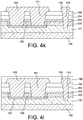
- the Figures 7a, 7b and 7c illustrate three examples of conformation of the mesa 130.
- the mesa takes on a truncated pyramid shape with a square base while on the Figure 7b and 7c , the mesa takes respectively a frustoconical and truncated form of prism.
- FIGS 7d to 7f and the figure 8 illustrate possibilities of the invention in which the structure comprises several mesas 130a, 130b, 130c each forming a Fabry-Perot type cavity each associated with a semiconductor junction.
- the mesas may have the same form factor and according to a second possibility of the invention, not illustrated, the mesas may have different form factors.
- the mesas 130a, 130b, 130c have the same form factor adapted for the first operating range.
- each of the cavities formed by one of the mesas makes it possible to focus a portion of the electromagnetic radiation received by the structure making it possible to increase the area on which the radiation is collected.
- electromagnetic the arrangement of the cavities being able to be periodic, the periodicity will preferentially be different from ⁇ 0 / n i with the optical index of the zone of reception of the electromagnetic radiation, that is to say the optical index of the support.
- the mesas of the same structure each having a different form factor, focus the electromagnetic radiation received by the structure on a different wavelength range and thus make it possible to increase the range of wavelengths in which the structure works.
- each of the junctions by the focusing of the radiation in a given wavelength range, will be mainly sensitive to the electromagnetic radiation in said given wavelength, the signals of the different junctions adding up, the structure presents a sensitivity over a range of wavelengths having the wavelength ranges of each of the cavities.
- the material forming each of the mesas 130a, b, c has a forbidden bandwidth whose energy is lower than that of an electromagnetic radiation included in the wavelength range comprising the lowest energy .
- the first and second semiconductor layers have a forbidden bandwidth whose energy is greater than the energy of an electromagnetic radiation 2 whose wavelength is in the range of wavelengths comprising the most high energy.
- the structure 10 may not have a part, or all, of the stack formed by the first, the second and the third insulating layer 153, 154, 155 which is in contact with the top of the mesa 130. Indeed, such a stack not participating in the confinement of the Fabry-Pérot cavity, its absence does not influence the operation of the structure.
- the structure 10 may have a second semiconductor layer 122 of reduced size vis-à-vis a structure 10 according to the first embodiment.
- the manufacturing method of a structure 10 according to the second embodiment differs from the method of manufacturing a structure 10 according to the first embodiment in that it comprises an additional step consisting, after deposition of the first insulating layer. 153, to remove the portion of the stack formed by the first insulating layer 153 and the third semiconductor layer 123, which is not at the region 121a of the first semiconductor layer 121.
- the second insulating layer 154 is in contact, for its part which is not at the level of the region 121a of the first semiconductor layer 121, with the first semiconductor layer 121 on its face which is opposite to support 100.
- Such a structure 10 has the advantage, compared to a structure according to the prior art, to present a second semiconductor layer 122 of reduced volume.
- a second semiconductor layer 122 whose volume is reduced limits the dark current that could be generated in said second semiconductor layer 122.
- the reflective sides of each of the Fabry-Perot type cavities are obtained by means of a reflective zone.
- the reflective sides of each of the cavities are formed by means of Bragg mirrors. Such Bragg mirrors may be formed, for example, by a stack of semiconductor layers.
- the mesa or mesas are partially or completely free of contact with the insulating layers 153, 154, 155.
- the structure has no support. According to this possibility, the electromagnetic radiation is received by the structure through an air zone of optical index n i equal to 1.
Description
L'invention se rapporte au domaine de la détection et/ou de la mesure de rayonnements électromagnétiques et aux dispositifs permettant une telle détection et/ou mesure.The invention relates to the field of the detection and / or measurement of electromagnetic radiation and devices for such detection and / or measurement.
L'évolution rapide de l'optoélectronique, liée à l'adaptation des technologies de la micro-électronique aux semiconducteurs à gap direct, a permis une amélioration des performances de détection et/ou de mesure des dispositifs permettant la détection et/ou la mesure de rayonnements électromagnétiques quelle que soit leur gamme de longueurs d'ondes.The rapid evolution of optoelectronics, related to the adaptation of micro-electronic technologies to direct-gap semiconductors, has led to an improvement in the detection and / or measurement performance of devices allowing detection and / or measurement. electromagnetic radiation irrespective of their wavelength range.
Ces dispositifs mettent généralement en œuvre des structures semiconductrices aptes à recevoir un rayonnement électromagnétique et à le transformer en un signal électrique.These devices generally implement semiconductor structures capable of receiving electromagnetic radiation and transforming it into an electrical signal.
L'invention se rapporte plus particulièrement à une structure semiconductrice, à un composant semiconducteur et à un procédé de fabrication d'une telle structure semiconductrice.The invention relates more particularly to a semiconductor structure, a semiconductor component and a method of manufacturing such a semiconductor structure.
Les structures semiconductrices adaptées pour recevoir un rayonnement électromagnétique comprennent généralement une première et une seconde zone semiconductrice en contact l'une de l'autre et présentant respectivement un premier et un second type de conductivité opposés l'un de l'autre. De cette manière la première et la seconde zone forment ensemble, au niveau de leur contact, une jonction semiconductrice.Semiconductor structures adapted to receive electromagnetic radiation generally comprise a first and a second semiconductor region in contact with each other and having respectively a first and a second conductivity type opposite to each other. In this way the first and the second zone together form, at their contact, a semiconductor junction.
Ainsi, pour un support dont le matériau semiconducteur est un matériau semiconducteur à gap direct et pour une polarisation inverse de la jonction, lorsqu'un photon, ayant une énergie supérieure à celle de la bande interdite du matériau semiconducteur, pénètre la jonction semiconductrice, celui-ci va générer une paire électron-trou qui, en raison du champ électrique régnant dans la structure, diffuse dans la structure de manière à former un courant photogénéré. Ce courant, étant directement proportionnel au rayonnement électromagnétique, fournit une mesure de ce même rayonnement électromagnétique.Thus, for a support whose semiconductor material is a direct gap semiconductor material and for a reverse bias of the junction, when a photon, having an energy higher than that of the forbidden band of the semiconductor material, penetrates the semiconductor junction, the latter will generate an electron-hole pair which, due to the electric field prevailing in the structure, diffuses into the structure to form a photogenerated stream. This current, being directly proportional to the electromagnetic radiation, provides a measurement of this same electromagnetic radiation.
On entend par matériau semiconducteur à gap direct un matériau semiconducteur dont le maximum d'énergie de la bande de valence et le minimum d'énergie de la bande de conduction se situent à une valeur du vecteur d'onde k sensiblement égale dans le diagramme de dispersion énergétique dudit matériau semiconducteur.By direct gap semiconductor material is meant a semiconductor material whose maximum energy of the valence band and the minimum of energy of the conduction band are at a substantially equal value of the wave vector k in the FIG. energy dispersion of said semiconductor material.
Si une telle technologie est bien adaptée pour la détection et la mesure de rayonnements électromagnétiques, elle possède néanmoins l'inconvénient de présenter un courant d'obscurité non nul, ce qui participe à dégrader le rapport signal sur bruit. Le courant d'obscurité a pour origine la génération de paires électron-trou non photo-générées dans la structure. Or cette génération a principalement lieu dans la zone active de la structure dans laquelle les photons sont absorbés pour générer le signal. Cette zone, pour maximiser le signal, doit occuper une grande partie du volume de la structure, celle-ci s'étendant généralement sur la quasi-totalité de la surface de la structure, et est donc à l'origine d'un bruit important.If such a technology is well suited for the detection and measurement of electromagnetic radiation, it nevertheless has the disadvantage of having a non-zero dark current, which contributes to degrade the signal-to-noise ratio. The dark current originates from the generation of non-photo-generated electron-hole pairs in the structure. But this generation takes place mainly in the active zone of the structure in which the photons are absorbed to generate the signal. This zone, to maximize the signal, must occupy a large part of the volume of the structure, which generally extends over almost the entire surface of the structure, and is therefore at the origin of a significant noise .
Ceci est d'autant plus vrai pour les structures adaptées pour fonctionner dans les longueurs d'onde infrarouge, ces dernières étant sujettes à un bruit important en raison de la faible largeur de bande interdite du matériau dans lequel elles sont formées. En effet, une faible largeur de bande interdite favorise la formation d'un courant d'obscurité tunnel dans la zone active.This is especially true for structures adapted to operate in infrared wavelengths, the latter being subject to significant noise due to the small bandgap of the material in which they are formed. Indeed, a small forbidden bandwidth promotes the formation of a tunnel dark current in the active zone.
Pour remédier à cet inconvénient, il est connu de concentrer le rayonnement électromagnétique dans une zone réduite de la structure dans laquelle est ménagée la jonction et donc la zone active. Ainsi, la structure peut recevoir le rayonnement électromagnétique sur une surface importante sans pour autant nécessiter une zone active occupant un volume important.To remedy this drawback, it is known to concentrate the electromagnetic radiation in a reduced area of the structure in which the junction and thus the active zone are arranged. Thus, the structure can receive electromagnetic radiation over a large area without requiring an active area occupying a large volume.
Une telle concentration du rayonnement électromagnétique peut être notamment obtenue, comme cela est décrit dans le document
Si le document
Il en résulte que si une telle structure présente, par rapport à une simple diode inversée, une réduction du courant d'obscurité, cette réduction est également accompagnée par une réduction du taux d'absorption du rayonnement électromagnétique. Le gain en rapport signal sur bruit apporté par cette solution, par rapport à une simple diode inversée, est donc réduit en raison de la faible épaisseur de la zone active sur laquelle le rayonnement électromagnétique est absorbé.As a result, if such a structure has, compared with a simple inverted diode, a reduction in the dark current, this reduction is also accompanied by a reduction in the absorption rate of the electromagnetic radiation. The gain in signal-to-noise ratio brought by this solution, compared with a simple inverted diode, is therefore reduced because of the small thickness of the active zone on which the electromagnetic radiation is absorbed.
La présente invention vise à remédier à cet inconvénient.The present invention aims to remedy this disadvantage.
Un but de l'invention est de fournir une structure semiconductrice qui présente un rapport signal sur bruit optimisé par rapport aux structures de l'art antérieur.An object of the invention is to provide a semiconductor structure which has an optimized signal-to-noise ratio with respect to the structures of the prior art.
A cet effet l'invention se rapporte à une structure semiconductrice telle que définie dans la revendication 1. Cette structure est destinée à recevoir un rayonnement électromagnétique dans une première gamme de longueurs d'onde, dite de fonctionnement, qui est centrée autour d'une longueur d'onde λ0, et comporte :
- une première zone semiconductrice d'un premier type de conductivité,
- une deuxième zone semiconductrice d'un deuxième type de conductivité opposé au premier type de conductivité, la deuxième zone semiconductrice étant en contact avec la première zone semiconductrice de manière à former une jonction semiconductrice,
ladite portion de la deuxième zone semiconductrice étant essentiellement ménagée dans une première cavité adaptée pour focaliser dans la première cavité une partie du champ électromagnétique reçu.For this purpose, the invention relates to a semiconductor structure as defined in
- a first semiconductor zone of a first conductivity type,
- a second semiconductor zone of a second conductivity type opposite to the first conductivity type, the second semiconductor zone being in contact with the first semiconductor zone so as to form a semiconductor junction,
said portion of the second semiconductor zone being essentially formed in a first cavity adapted to focus in the first cavity part of the electromagnetic field received.
L'aménagement de la deuxième zone semiconductrice dans une première cavité adaptée pour concentrer le champ électromagnétique et le fait que la portion de la deuxième zone semiconductrice présente une concentration en porteurs majoritaires réduite par rapport à la première zone semiconductrice, permettent à la structure de présenter sa zone active, formée par la zone de charge d'espace de la jonction, principalement comprise dans la cavité. En effet, la deuxième zone semiconductrice présentant une portion avec une concentration en porteurs majoritaires réduite, la zone de charge d'espace, correspondant à la zone active, s'étend principalement dans cette portion.The arrangement of the second semiconductor zone in a first cavity adapted to concentrate the electromagnetic field and the fact that the portion of the second semiconductor zone has a reduced majority carrier concentration relative to the first semiconductor zone, allow the structure to present its active zone, formed by the space charge area of the junction, mainly comprised in the cavity. Indeed, the second semiconductor zone having a portion with a reduced majority carrier concentration, the space charge area, corresponding to the active area, extends mainly in this portion.
De plus, la relativement faible concentration en porteurs majoritaires de la portion de deuxième zone semiconductrice induit une déplétion des porteurs majoritaires dans cette même portion de la deuxième zone semiconductrice, limitant ainsi les risques de recombinaisons paires électron-trou qui est la source du courant d'obscurité. On peut enfin noter qu'une telle configuration de la structure, par la courbure de bande induite le long de la portion de la deuxième zone semiconductrice permet une collection des porteurs minoritaires photogénérés par écoulement de ces derniers le long de la portion et non par diffusion. Le temps de collection s'en trouve réduit, par rapport à une structure collectant le courant photogénéré par diffusion de porteurs. La réponse de la structure est donc fiabilisée vis-à-vis des structures de l'art antérieur qui présentent une probabilité plus importante de recombinaison des paires électron-trou photogénérées avant leur collection. Il en résulte qu'une structure selon l'invention permet un étalonnage reproductible avec une sensibilité accrue vis-à-vis d'une structure selon l'art antérieur.In addition, the relatively low concentration of majority carriers of the portion of the second semiconductor zone induces a depletion of the majority carriers in this same portion of the second semiconductor zone, thus limiting the risks of electron-hole pair recombinations which is the source of the current. darkness. Finally, it can be noted that such a configuration of the structure, by the induced curvature of the strip along the portion of the second semiconducting zone allows a collection of photogenerated minority carriers by flow of the latter along the portion and not by diffusion. . The collection time is reduced compared to a structure collecting the photogenerated current by carrier diffusion. The response of the structure is thus reliable with respect to the structures of the prior art which have a greater probability of recombination of the photogenerated electron-hole pairs before their collection. As a result, a structure according to the invention allows a reproducible calibration with increased sensitivity to a structure according to the prior art.
Une cavité comprise dans un composant optoélectronique peut être une cavité résonante ou optique, telle qu'une cavité du type Fabry-Pérot. Ainsi une telle cavité n'est donc pas forcément vide puisque pouvant contenir, par exemple, un milieu actif comme c'est le cas pour un composant du type laser semiconducteur.A cavity comprised in an optoelectronic component may be a resonant or optical cavity, such as a Fabry-Perot type cavity. Thus such a cavity is not necessarily empty since it may contain, for example, an active medium as is the case for a component of the semiconductor laser type.
Par focalisation on entend, dans le domaine de l'optique et de l'optoélectronique, le fait de faire converger un faisceau lumineux de manière à le concentrer dans un faible volume.By focusing is meant, in the field of optics and optoelectronics, the fact of converging a light beam so as to concentrate it in a small volume.
Par ailleurs, il est possible, à niveau signal sur bruit équivalent, d'augmenter la température de fonctionnement du dispositif.Moreover, it is possible, at equivalent signal-on-noise level, to increase the operating temperature of the device.
Par portion essentiellement ménagée dans la cavité, on entend que la portion est au moins en partie disposée dans la cavité, la portion de la deuxième zone semiconductrice présentant plus de la moitié de son volume ménagée dans la première cavité.By portion essentially formed in the cavity is meant that the portion is at least partly disposed in the cavity, the portion of the second semiconductor zone having more than half of its volume in the first cavity.
La portion de la deuxième zone semiconductrice représente la majeure partie de la deuxième zone semiconductrice qui est ménagée dans la première cavité.The portion of the second semiconductor zone represents most of the second semiconductor zone which is formed in the first cavity.
La première cavité est une cavité du type Fabry-Pérot particulièrement adaptée pour permettre une concentration d'un champ électromagnétique.The first cavity is a Fabry-Perot type cavity particularly adapted to allow a concentration of an electromagnetic field.
La première cavité présente selon au moins une direction de confinement une dimension moyenne sensiblement égale à λ0/2neff avec neff l'indice effectif moyen dans la deuxième zone semiconductrice.The first cavity has, in at least one confinement direction, a dimension mean substantially equal to λ 0 / 2n eff with n eff the average effective index in the second semiconductor zone.
Une cavité Fabry-Pérot dont la dimension moyenne est sensiblement égale à λ0/2neff est particulièrement adaptée pour concentrer un rayonnement électromagnétique dont la longueur d'onde est comprise dans la gamme de fonctionnement.A Fabry-Perot cavity whose average dimension is substantially equal to λ 0 / 2n eff is particularly suitable for concentrating an electromagnetic radiation whose wavelength is within the operating range.
La structure étant destinée à recevoir le rayonnement électromagnétique selon une direction moyenne de réception, la direction de confinement peut être sensiblement perpendiculaire à la direction moyenne de réception.Since the structure is intended to receive the electromagnetic radiation in an average reception direction, the confinement direction may be substantially perpendicular to the average reception direction.
Une telle orientation de la dimension de confinement permet d'obtenir un confinement de la structure selon une direction perpendiculaire de la jonction autorisant le dimensionnement au besoin de l'épaisseur selon laquelle s'étend la portion, limitant ainsi la partie du rayonnement électromagnétique qui ne serait pas absorbée lors de son passage dans la structure.Such an orientation of the confinement dimension makes it possible to obtain a confinement of the structure in a perpendicular direction of the junction allowing the dimensioning, if necessary, of the thickness according to which the portion extends, thus limiting the part of the electromagnetic radiation which does not would not be absorbed during his passage in the structure.
On peut également noter que dans la configuration dans laquelle la jonction s'étend sensiblement dans le plan de la surface de la structure, une telle direction de la dimension de la cavité permet une focalisation de la composante transverse électrique (TE) du champ électromagnétique.It may also be noted that in the configuration in which the junction extends substantially in the plane of the surface of the structure, such a direction of the dimension of the cavity allows a focusing of the transverse electrical component (TE) of the electromagnetic field.
La dimension de la première cavité selon la direction de confinement est une dimension variable, ladite dimension diminuant préférentiellement de la première zone semiconductrice vers la deuxième zone semiconductrice.The dimension of the first cavity in the direction of confinement is a variable dimension, said dimension preferably decreasing from the first semiconductor zone to the second semiconductor zone.
Une telle dimension variable permet d'élargir la gamme de longueurs d'onde du rayonnement électromagnétique qui est focalisé dans la première cavité.Such a variable dimension makes it possible to widen the range of wavelengths of the electromagnetic radiation which is focused in the first cavity.
La dimension de la première cavité selon la direction de confinement varie sensiblement monotonement selon la direction allant de la première zone semiconductrice vers la deuxième zone semiconductrice.The dimension of the first cavity in the confinement direction varies substantially monotonously in the direction from the first semiconductor zone to the second semiconductor zone.
La dimension de la première cavité selon la direction de confinement varie selon un angle compris entre 0 et 40° par rapport à la direction allant de la première zone semiconductrice vers la deuxième zone semiconductrice.The dimension of the first cavity in the direction of confinement varies at an angle between 0 and 40 ° with respect to the direction from the first semiconductor zone to the second semiconductor zone.
La jonction peut être une hétérojonction.The junction can be a heterojunction.
Un tel type de jonction permet d'adapter la largeur de bande interdite de chaque zone semiconductrice et peut permettre d'optimiser la partie du rayonnement électromagnétique absorbée par la zone semiconductrice fonctionnelle de la jonction.Such a type of junction makes it possible to adapt the bandgap width of each semiconductor zone and can make it possible to optimize the portion of the electromagnetic radiation absorbed by the semiconductor functional zone of the junction.
La première et la deuxième zone semiconductrice peuvent présenter des largeurs de bande interdite d'énergies différentes, la deuxième zone semiconductrice peut présenter une largeur de bande interdite moyenne d'énergie supérieure à celle d'un rayonnement dont la longueur d'onde est comprise dans la gamme de fonctionnement.The first and second semiconducting zone may have bandgap widths of different energies, the second semiconductor zone may have an average energy gap bandwidth greater than that of a radiation whose wavelength is within the operating range.
On entend ci-dessus et dans le reste de ce document par énergie correspondant à la largeur de bande interdite, la différence d'énergie entre le minimum d'énergie de la bande de conduction et le maximum d'énergie de la bande de valence ceci à la température à laquelle est destinée à fonctionner la structure semiconductrice.We hear above and in the rest of this document by energy corresponding to the forbidden bandwidth, the energy difference between the minimum energy of the conduction band and the maximum energy of the valence band this at the temperature at which the semiconductor structure is intended to operate.
Ainsi le rayonnement électromagnétique, dans une configuration dans laquelle le rayonnement électromagnétique traverse la première zone semiconductrice avant d'arriver dans la deuxième zone semiconductrice, présente une atténuation réduite lors de son passage au travers de la première zone semiconductrice.Thus, the electromagnetic radiation, in a configuration in which the electromagnetic radiation passes through the first semiconductor zone before arriving in the second semiconductor zone, has a reduced attenuation as it passes through the first semiconductor zone.
La première et la deuxième zone semiconductrice peuvent présenter des largeurs de bande interdite d'énergies différentes, la première zone semiconductrice présentant une largeur de bande interdite moyenne d'énergie inférieure à celle d'un rayonnement dont la longueur d'onde est comprise dans la gamme de fonctionnement.The first and the second semiconductor zone may have bandgap widths of different energies, the first semiconductor zone having a mean energy band gap width smaller than that of a radiation whose wavelength is within operating range.
Ainsi la deuxième zone semiconductrice est particulièrement adaptée pour l'absorption du rayonnement électromagnétique.Thus the second semiconductor zone is particularly suitable for the absorption of electromagnetic radiation.
la deuxième zone semiconductrice comporte, outre ladite portion, une partie non ménagée dans la cavité et présentant une largeur de bande interdite moyenne d'énergie supérieure à celle d'un rayonnement électromagnétique dont la longueur d'onde est comprise dans la gamme de fonctionnement, et ladite portion présentant une largeur de bande interdite moyenne d'énergie inférieure à celle d'un rayonnement électromagnétique dont la longueur d'onde est comprise dans la première gamme de fonctionnement.the second semiconductor zone comprises, in addition to said portion, a non-sparse portion in the cavity and having a mean energy band gap width greater than that of electromagnetic radiation whose wavelength is within the operating range, and said portion having an average energy gap bandwidth less than that of a electromagnetic radiation whose wavelength is within the first operating range.
Avec une telle configuration de la deuxième zone semiconductrice, l'absorption de rayonnement à lieu uniquement dans la cavité.With such a configuration of the second semiconductor zone, the absorption of radiation takes place only in the cavity.
La première zone semiconductrice peut présenter une largeur de bande interdite qui diminue en direction de la deuxième zone semiconductrice.The first semiconductor zone may have a band gap that decreases towards the second semiconductor zone.
Le rayonnement électromagnétique est reçu dans un milieu d'indice optique ni, dit indice incident, le rapport entre l'indice effectif et l'indice incident neff/ni étant supérieur à 1, préférentiellement sensiblement supérieur à 1,5, et encore plus préférentiellement supérieur à 2.The electromagnetic radiation is received in a medium of optical index n i , said incident index, the ratio between the effective index and the incident index n eff / n i being greater than 1, preferably substantially greater than 1.5, and still more preferably greater than 2.
Avec une réception du rayonnement dans un milieu d'indice optique ni, un tel rapport entre l'indice effectif neff et l'indice incident ni permet de fournir une bonne focalisation du rayonnement électromagnétique dans la cavité.With a reception of the radiation in an optical index medium n i , such a ratio between the effective index n eff and the incident index n i makes it possible to provide a good focusing of the electromagnetic radiation in the cavity.
On entend ci-dessus et dans le reste de ce document, par indice optique d'un milieu, l'indice de réfraction du milieu pour la première gamme de longueurs d'onde.Above and in the remainder of this document, the optical index of a medium means the refractive index of the medium for the first range of wavelengths.
Le milieu d'indice incident ni peut être un support de la structure.The incident index medium n i may be a support of the structure.
Le milieu d'indice incident ni peut être une zone d'air au travers de laquelle le rayonnement est reçu par la structure.The incident index medium n i may be an air zone through which the radiation is received by the structure.
Les première et deuxième zones semiconductrices peuvent être réalisées dans des matériaux semiconducteurs composés essentiellement d'au moins trois mêmes éléments dont la concentration en au moins l'un de ces éléments permet de faire varier la largeur de bande interdite, lesdits éléments étant préférentiellement le cadmium (Cd), le mercure (Hg) et le tellure (Te).The first and second semiconductor zones can be produced in semiconductor materials composed essentially of at least three same elements whose concentration in at least one of these elements makes it possible to vary the forbidden band width, said elements being preferably cadmium (Cd), mercury (Hg) and tellurium (Te).
De tels éléments autorisent, par une variation de la concentration d'au moins un de ces éléments, la modification de la largeur de bande interdite le long de la structure donnant accès ainsi à la possibilité d'optimiser cette largeur de bande interdite selon les zones semiconductrices de la structure et de leur fonction.Such elements allow, by varying the concentration of at least one of these elements, the modification of the band gap along the structure thus giving access to the possibility of optimizing this bandgap according to the zones semiconductors of the structure and their function.
En effet les tellurures de mercure-cadmium possèdent entre autres avantages de présenter une largeur de bande interdite qui varie avec la concentration en cadmium ceci sans que cela n'affecte leur propriété de semiconducteur à gap direct. Ainsi, il est possible en faisant varier les proportions en éléments que sont le tellure (Te), le cadmium (Cd) et le mercure (Hg) de former une hétérojonction avec une largeur de bande interdite de chacune des zones semiconductrices de la jonction qui est adaptée en fonction des besoins.Indeed mercury-cadmium tellurides have among other advantages to present a band gap that varies with the concentration in cadmium this without affecting their direct gap semiconductor property. Thus, it is possible by varying the proportions in elements that are tellurium (Te), cadmium (Cd) and mercury (Hg) to form a heterojunction with a forbidden band width of each semiconductor zone of the junction which is adapted according to the needs.
La gamme de fonctionnement peut être comprise dans la gamme de longueurs d'onde des infrarouges.The operating range may be in the infrared wavelength range.
Il peut être prévu :
- un support transparent dans la gamme de fonctionnement, le substrat comportant une première et une seconde face,
- une première couche semiconductrice du premier type de conductivité s'étendant le long de la première face en contact avec cette même première face, une portion de ladite première couche semiconductrice formant la première zone semiconductrice,
- un mesa semiconducteur en contact direct, ou par l'intermédiaire d'une deuxième couche semiconductrice du deuxième type de conductivité, avec la face de la première couche semiconductrice qui est opposée à la première face, ledit mesa présentant le deuxième type de conductivité et sur une partie du mesa une concentration en porteurs majoritaires qui est au moins dix fois inférieure à celle de la première couche semiconductrice, ledit mesa formant au moins partiellement la deuxième zone semiconductrice, le mesa présentant au moins une direction, la direction de confinement, selon laquelle le mesa présente une dimension moyenne de λ0/2neff, la partie du mesa formant au moins partiellement la portion de la deuxième zone semiconductrice,
- une zone, dite réfléchissante, réalisée dans un matériau au moins partiellement réfléchissant dans la gamme fonctionnement, la zone réfléchissante recouvrant au moins une partie du mesa de manière à former la première cavité de type Fabry-Pérot qui présente une dimension moyenne sensiblement égale à λ0/2neff selon la direction de confinement.
- a transparent medium in the operating range, the substrate having a first and a second face,
- a first semiconductor layer of the first conductivity type extending along the first face in contact with the same first face, a portion of said first semiconductor layer forming the first semiconductor zone,
- a semiconductor mesa in direct contact, or via a second semiconductor layer of the second conductivity type, with the face of the first semiconductor layer opposite to the first face, said mesa having the second conductivity type and on a part of the mesa a majority carrier concentration which is at least ten times lower than that of the first semiconductor layer, said mesa forming at least partially the second semiconductor zone, the mesa having at least one direction, the confinement direction, according to which the mesa has an average dimension of λ 0 / 2n eff , the part of the mesa forming at least partially the portion of the second semiconductor zone,
- a so-called reflecting zone made of a material that is at least partially reflective in the operating range, the reflecting zone covering at least a portion of the mesa so as to form the first Fabry-Pérot type cavity which has an average dimension substantially equal to λ 0 / 2n eff according to the direction of confinement.
Une telle structure est particulièrement adaptée aux contraintes de fabrication de l'opto-électronique.Such a structure is particularly adapted to the manufacturing constraints of optoelectronics.
Il peut être prévu une deuxième couche semiconductrice en contact avec la surface de la première face qui est opposée à la première face, le mesa étant en contact direct avec la deuxième couche semiconductrice et en contact avec la première couche semiconductrice au travers de la deuxième couche semiconductrice, la deuxième couche présentant au moins une partie dont la concentration en porteurs majoritaires est dix fois inférieure à celle de première couche semiconductrice, la deuxième couche semiconductrice et le mesa formant la deuxième zone semiconductrice et les parties respectifs du mesa et de la deuxième couche semiconductrice formant la portion de la deuxième zone semiconductrice.It can be provided a second semiconductor layer in contact with the surface of the first face which is opposite the first face, the mesa being in direct contact with the second semiconductor layer and in contact with the first semiconductor layer through the second layer semiconductor, the second layer having at least one portion whose concentration of majority carriers is ten times lower than that of the first semiconductor layer, the second semiconductor layer and the mesa forming the second semiconductor zone and the respective parts of the mesa and the second layer. semiconductor forming the portion of the second semiconductor zone.
Le mesa peut être en contact direct avec la première couche semiconductrice.The mesa may be in direct contact with the first semiconductor layer.
Il peut être en outre prévu au moins une troisième et une quatrième zone semiconductrice présentant respectivement le premier et le deuxième type de conductivité, la troisième et la quatrième zone semiconductrice étant en contact l'une avec l'autre de manière à former une jonction semiconductrice, la quatrième zone semiconductrice présente une deuxième portion dont la concentration en porteurs majoritaires est au moins inférieure de dix fois la concentration en porteurs majoritaires de la troisième zone semiconductrice, ladite deuxième portion étant la portion de la quatrième zone semiconductrice qui est en contact avec la troisième zone semiconductrice, la quatrième zone semiconductrice est essentiellement ménagée dans une deuxième cavité, ladite deuxième cavité étant adaptée pour concentrer dans la deuxième cavité une partie du rayonnement électromagnétique qui est reçu par la structure et dont la longueur d'onde est comprise dans une gamme de longueurs d'onde dite deuxième gamme de fonctionnement.In addition, at least a third and a fourth semiconductor zone having the first and second conductivity types, the third and fourth semiconducting regions being in contact with one another so as to form a semiconductor junction may be provided. the fourth semiconductor zone has a second portion whose concentration in majority carriers is at least 10 times lower than the majority carrier concentration of the third semiconductor zone, said second portion being the portion of the fourth semiconductor zone which is in contact with the third semiconductor zone, the fourth semiconductor zone is essentially formed in a second cavity, said second cavity being adapted to concentrate in the second cavity part of the electromagnetic radiation which is received by the structure and whose wavelength is within a range of length waveforms said second operating range.
De telles troisième et quatrième zones semiconductrices et la deuxième cavité qui leur est associée, permettent d'augmenter la surface de la structure sur laquelle le rayonnement électromagnétique est collecté et donc le signal fourni par la structure lorsque cette dernière reçoit un rayonnement électromagnétique.Such third and fourth semiconductor zones and the second cavity associated therewith, allow to increase the surface of the structure on which the electromagnetic radiation is collected and therefore the signal provided by the structure when the latter receives electromagnetic radiation.
Elles permettent également, pour une deuxième gamme de fonctionnement différente de la première gamme de fonctionnement de fournir une structure adaptée pour recevoir un rayonnement électromagnétique à la fois dans la première gamme de fonctionnement et dans la deuxième gamme de fonctionnement.They also allow for a second operating range different from the first operating range to provide a structure adapted to receive electromagnetic radiation in both the first operating range and the second operating range.
La deuxième gamme de fonctionnement est sensiblement identique à la première gamme de fonctionnement.The second operating range is substantially the same as the first operating range.
Ainsi, la structure présente, pour les rayonnements électromagnétiques dont la longueur d'onde est comprise dans la première gamme de fonctionnement, une surface de réception de ces rayonnements électromagnétiques qui est augmentée par rapport à une structure ne comportant pas une deuxième cavité adaptée pour focaliser dans la deuxième cavité une partie du rayonnement électromagnétique qui est reçue par la structure et dont la longueur d'onde est comprise dans la première gamme de fonctionnement.Thus, the structure has, for electromagnetic radiation whose wavelength is in the first operating range, a receiving surface of these electromagnetic radiations which is increased relative to a structure not comprising a second cavity adapted to focus. in the second cavity a portion of the electromagnetic radiation which is received by the structure and whose wavelength is in the first operating range.
La deuxième gamme de fonctionnement peut être différente de la première gamme de fonctionnement, la première et la deuxième gamme de fonctionnement étant préférentiellement choisies pour couvrir une gamme de longueurs d'onde continue.The second operating range may be different from the first operating range, the first and second operating range being preferably selected to cover a continuous wavelength range.
Ainsi, la structure est adaptée pour la réception de rayonnements électromagnétiques sur une gamme de longueurs d'onde de plus grande largeur qu'une structure ne comportant pas de deuxième cavité.Thus, the structure is adapted for the reception of electromagnetic radiation over a wavelength range of greater width than a structure having no second cavity.
L'invention concerne également un composant semiconducteur comportant une pluralité de structures semiconductrices destinées à recevoir un rayonnement électromagnétique, au moins l'une des structures étant une structure selon l'invention.The invention also relates to a semiconductor component comprising a plurality of semiconductor structures for receiving electromagnetic radiation, at least one of the structures being a structure according to the invention.
Un tel composant, présente, pour la ou les structures selon l'invention, un rapport signal sur bruit optimisé vis-à-vis d'un composant comportant uniquement des structures selon l'art antérieur.Such a component has, for the structure or structures according to the invention, a signal-to-noise ratio optimized vis-à-vis a component comprising only structures according to the prior art.
L'invention concerne également un procédé de fabrication d'une structure destinée à recevoir un rayonnement électromagnétique dans une première gamme de longueurs d'onde, dite de fonctionnement, qui est centrée autour d'une longueur d'onde λ0, le procédé comportant les étapes consistant à :
- Fournir un support présentant une première et une seconde face,
- Former une première couche semiconductrice d'un premier type de conductivité, au moins une portion de ladite couche semiconductrice formant une première zone semiconductrice,
- Former un mesa semiconducteur en contact avec la couche semiconductrice, ledit mesa étant d'un deuxième type de conductivité opposé au premier type de conductivité et comportant une portion, en contact avec la première couche semiconductrice, dont la concentration en porteurs majoritaires est au moins inférieure de dix fois la concentration en porteurs majoritaires de la première couche semiconductrice, le mesa présentant au moins une direction, dite de confinement, selon laquelle le mesa présente une dimension moyenne de λ0/2neff, le mesa formant avec au moins partiellement une deuxième zone semiconductrice,
- déposer une couche d'un matériau au moins partiellement réfléchissant dans la gamme de fonctionnement de manière à former une zone dite réfléchissante, la zone réfléchissante recouvrant au moins une partie du mesa de manière à former une première cavité de type Fabry-Pérot qui présente une dimension moyenne sensiblement égale à λ0/2neff selon la direction de confinement.
- Provide a support with a first and a second face,
- Forming a first semiconductor layer of a first conductivity type, at least a portion of said semiconductor layer forming a first semiconductor zone,
- Forming a semiconductor mesa in contact with the semiconductor layer, said mesa being of a second conductivity type opposite to the first conductivity type and having a portion, in contact with the first semiconductor layer, whose majority carrier concentration is at least lower; ten times the majority carrier concentration of the first semiconductor layer, the mesa having at least one so-called confinement direction, according to which the mesa has an average dimension of λ 0 / 2n eff , the mesa forming with at least partially a second semiconductor zone,
- depositing a layer of at least partially reflective material in the operating range so as to form a so-called reflecting zone, the reflecting zone covering at least a portion of the mesa so as to form a first Fabry-Perot type cavity which has a average dimension substantially equal to λ 0 / 2n eff according to the confinement direction.
Un tel procédé permet la formation d'une structure présentant dans la gamme de fonctionnement un rapport signal sur bruit amélioré vis-à-vis d'une structure de l'art antérieur.Such a method allows the formation of a structure having in the operating range an improved signal-to-noise ratio with respect to a structure of the prior art.
Le procédé de fabrication peut comporter entre l'étape de formation de la première couche semiconductrice et l'étape de formation du mesa, une étape de formation d'une deuxième couche semiconductrice du deuxième type de conductivité en contact avec la première couche semiconductrice sur la face de la première couche semiconductrice qui est opposée au support, le mesa étant formé en contact avec la deuxième couche semiconductrice.The manufacturing method may comprise between the step of forming the first semiconductor layer and the step of forming the mesa, a step of forming a second semiconductor layer of the second conductivity type in contact with the first semiconductor layer on the face of the first semiconductor layer opposite to the support, the mesa being formed in contact with the second semiconductor layer.
Alternativement le procédé de fabrication d'une structure destinée à recevoir un rayonnement électromagnétique dans une première gamme de longueurs d'onde, dite de fonctionnement, qui est centrée autour d'une longueur d'onde λ0, peut comporter les étapes consistant à :
- fournir un support présentant une première et une seconde face,
- former une première couche semiconductrice d'un premier type de conductivité, au moins une portion de ladite première couche semiconductrice formant une première zone semiconductrice,
- former une deuxième couche semiconductrice en contact avec la première couche semiconductrice, ladite deuxième couche semiconductrice étant d'un deuxième type de conductivité qui est opposé au premier type de conductivité, au moins une partie de la deuxième couche semiconductrice qui est en contact avec la première couche semiconductrice présentant une concentration en porteurs majoritaires qui est au moins inférieure de dix fois la concentration en porteurs majoritaires de la première couche semiconductrice,
- former un mesa semiconducteur en contact avec la partie de la deuxième couche semiconductrice, ledit mesa étant du deuxième type de conductivité et comportant au moins une partie, en contact avec la partie de la deuxième couche semiconductrice, dont la concentration en porteurs majoritaires est au moins inférieure de dix fois la concentration en porteurs majoritaires de la première couche semiconductrice, le mesa présentant au moins une direction, dite de confinement, selon laquelle le mesa présente une dimension moyenne de λ0/2neff, le mesa formant avec la deuxième couche semiconductrice au moins partiellement une deuxième zone semiconductrice et la partie du mesa formant avec la partie de la deuxième couche semiconductrice une portion de la deuxième zone,
- déposer une couche d'un matériau au moins partiellement réfléchissant dans la gamme de fonctionnement, ladite couche recouvrant au moins une partie du mesa de manière à former une première cavité de type Fabry-Pérot qui présente une dimension moyenne sensiblement égale à λ0/2neff selon la direction de confinement.
- provide a support having first and second faces,
- forming a first semiconductor layer of a first conductivity type, at least a portion of said first semiconductor layer forming a first semiconductor zone,
- forming a second semiconductor layer in contact with the first semiconductor layer, said second semiconductor layer being of a second conductivity type which is opposite to the first conductivity type, at least a part of the second semiconductor layer which is in contact with the first semiconductor layer having a majority carrier concentration which is at least ten times lower than the majority carrier concentration of the first semiconductor layer,
- forming a semiconductor mesa in contact with the portion of the second semiconductor layer, said mesa being of the second conductivity type and having at least a portion, in contact with the portion of the second semiconductor layer, whose majority carrier concentration is at least 10 times lower than the majority carrier concentration of the first semiconductor layer, the mesa having at least one so-called confinement direction, in which the mesa has an average dimension of λ 0 / 2n eff , the mesa forming with the second semiconductor layer at least partially a second semiconductor zone and the part of the mesa forming with the part of the second semiconductor layer a portion of the second zone,
- depositing a layer of at least partially reflective material in the operating range, said layer covering at least a portion of the mesa so as to form a first Fabry-Perot type cavity having an average dimension substantially equal to λ 0 / 2n eff according to the direction of containment.
Il peut être prévu avant l'étape de formation de la deuxième couche semiconductrice une étape de formation d'une troisième couche semiconductrice du premier type de conductivité en contact avec la première couche semiconductrice, la première couche et la troisième couche semiconductrice comportant une concentration en impuretés du type donneur de porteurs majoritaires du deuxième type de conductivité qui est au moins dix fois inférieure à la concentration en porteurs majoritaires desdites première et troisième couches semiconductrice, les étapes de formation du mesa et de la deuxième couche semiconductrice étant obtenues par gravure de la troisième couche conductrice et une partie de la première couche conductrice, cette étape de gravure étant adaptée pour inhiber les porteurs majoritaires du premier type de conductivité.It may be provided before the step of forming the second semiconductor layer a step of forming a third semiconductor layer of the first type of conductivity in contact with the first semiconductor layer, the first layer and the third semiconductor layer having a majority carrier-type impurity concentration of the second conductivity type that is at least ten times lower than the majority carrier concentration of said first and third semiconductor layers, the steps of forming the mesa and the second semiconductor layer being obtained by etching the third conductive layer and a part of the first conductive layer, this etching step being adapted to inhibit the majority carriers of the first type conductivity.
La présente invention sera mieux comprise à la lecture de la description d'exemples de réalisation, donnés à titre purement indicatif et nullement limitatif, en faisant référence aux dessins annexés sur lesquels :
- la
figure 1 illustre une vue en coupe d'un exemple de structure selon un premier mode de réalisation de l'invention, - la
figure 2 illustre la répartition en Cadmium le long de la structure illustrée sur lafigure 1 , - la
figure 3 illustre un exemple de configuration d'une structure selon le premier mode de réalisation de l'invention, - les
figures 4a à 4n illustrent les étapes d'un procédé de fabrication d'une structure telle qu'illustrée sur lafigure 1 , - la
figure 5 illustre un exemple de structure de bande le long d'une structure selon le premier mode de réalisation de l'invention, - la
figure 6 illustre un composant comportant plusieurs structures selon l'invention, - les
figures 7a à 7f illustrent des exemples de configuration de structures selon différentes possibilités de l'invention, - la
figure 8 illustre une coupe d'une structure selon une possibilité de l'invention dans laquelle la structure comporte plusieurs cavités, - les
figures 9a à 9d illustrent différentes étapes de fabrication d'une structure selon un deuxième mode de réalisation de l'invention.
- the
figure 1 illustrates a sectional view of an exemplary structure according to a first embodiment of the invention, - the
figure 2 illustrates the Cadmium distribution along the structure illustrated on thefigure 1 , - the
figure 3 illustrates an exemplary configuration of a structure according to the first embodiment of the invention, - the
Figures 4a to 4n illustrate the steps of a method of manufacturing a structure as illustrated on thefigure 1 , - the
figure 5 illustrates an example of a band structure along a structure according to the first embodiment of the invention, - the
figure 6 illustrates a component comprising several structures according to the invention, - the
Figures 7a to 7f illustrate examples of configuration of structures according to different possibilities of the invention, - the
figure 8 illustrates a section of a structure according to a possibility of the invention in which the structure comprises several cavities, - the
Figures 9a to 9d illustrate different steps of manufacturing a structure according to a second embodiment of the invention.
Des parties identiques, similaires ou équivalentes des différentes figures portent les mêmes références numériques de façon à faciliter le passage d'une figure à l'autre.Identical, similar or equivalent parts of the different figures bear the same numerical references so as to facilitate the passage from one figure to another.
Les différentes parties représentées sur les figures ne le sont pas nécessairement selon une échelle uniforme, pour rendre les figures plus lisibles.The different parts shown in the figures are not necessarily in a uniform scale, to make the figures more readable.
Les différentes possibilités (variantes et modes de réalisation) doivent être comprises comme n'étant pas exclusives les unes des autres et peuvent se combiner entre elles.The different possibilities (variants and embodiments) must be understood as not being exclusive of each other and can be combined with one another.
La
La première gamme de fonctionnement est une gamme de longueurs d'onde qui peut être comprise aussi bien dans la gamme de longueurs d'onde du visible, des ultraviolets ou encore des infrarouges. Dans l'application particulière illustrée sur la
Les caractéristiques et les valeurs qui sont mentionnées dans le reste de ce document, lorsqu'elles sont indiquées comme concernant l'application particulière, s'appliquent uniquement à cette application particulière et ne limitent donc en rien la portée de l'invention.The features and values that are mentioned in the rest of this document, when indicated as relevant to the particular application, apply only to that particular application and therefore do not limit the scope of the invention.
Une structure 10 selon ce premier mode de réalisation comporte :
un support 100, éventuellement semiconducteur, transparent dans la gamme de fonctionnement, le support comportant une première et une seconde face,- une première couche semiconductrice 121 du premier type de conductivité s'étendant le long de la première face du support en contact avec cette même première face,
- une deuxième couche semiconductrice 122 du deuxième type de conductivité s'étendant le long d'une région de la première couche en contact, dans ladite région, avec la face de la première couche qui est opposée à la première face du support,
- une troisième couche semiconductrice 123 en contact avec la première couche sur la face de première couche opposée au support, la troisième couche semiconductrice étant en contact sur la surface de ladite face qui n'est par recouverte par la deuxième couche semiconductrice,
un mesa 130 semiconducteur en contact avec la deuxième couche semiconductrice 122 sur la surface de la deuxième couche semiconductrice 122 qui est opposée à la première couche semiconductrice 121,ledit mesa 130 présentant le deuxième type de conductivité,une zone 141, dite réfléchissante, réalisée dans un matériau conducteur qui est au moins partiellement réfléchissant dans la gamme de fonctionnement,ladite zone réfléchissante 141 en contact avec lemesa 130 sur les côtés dumesa 130 et avec la deuxième couche semiconductrice 122 sur sa face qui est opposée à la première couche semiconductrice 121 dans la partie de ladite face qui n'est pas en contact avec lemesa 130, ledit matériau étant un matériau conducteur électriquement, lazone réfléchissante 141 formant un premier contact électrique,- une première et une seconde
zone isolante zone isolante 152 avec lemesa 130, - un deuxième
contact électrique 143 en contact avec la première couche semiconductrice 121 au travers de la première zone isolante 151 et de la troisième couche semiconductrice 123.
- a
support 100, possibly semiconductive, transparent in the operating range, the support comprising a first and a second face, - a
first semiconductor layer 121 of the first conductivity type extending along the first face of the support in contact with this same first face, - a
second semiconductor layer 122 of the second conductivity type extending along a region of the first layer in contact, in said region, with the face of the first layer which is opposite the first face of the support, - a
third semiconductor layer 123 in contact with the first layer on the first layer face opposite to the support, the third semiconductor layer being in contact on the surface of said face which is not covered by the second semiconductor layer, - a
semiconductor mesa 130 in contact with thesecond semiconductor layer 122 on the surface of thesecond semiconductor layer 122 which is opposite thefirst semiconductor layer 121, saidmesa 130 having the second conductivity type, - a so-called
reflective zone 141 made of a conductive material which is at least partially reflective in the operating range, said reflectingzone 141 in contact with themesa 130 on the sides of themesa 130 and with thesecond semiconductor layer 122 on its face which is opposed to thefirst semiconductor layer 121 in the portion of said face which is not in contact with themesa 130, said material being an electrically conductive material, the reflectingzone 141 forming a first electrical contact, - a first and a second insulating
zone zone 151 being in contact with thethird semiconductor layer 123 and the second insulatingzone 152 with themesa 130, - a second
electrical contact 143 in contact with thefirst semiconductor layer 121 through the first insulatingzone 151 and thethird semiconductor layer 123.
Le support semiconducteur 100 est un support classiquement utilisé pour les applications optoélectroniques. Le support est préférentiellement un substrat transparent dans la première gamme de fonctionnement. Le support 100 est réalisé dans un matériau semiconducteur classiquement utilisé pour les applications de l'optoélectronique, tel que par exemple, le silicium, le carbure de silicium, le saphir. Le support présente un indice optique, ou indice de réfraction, ni.The
Dans l'application particulière de l'invention, le support 100 est un substrat en tellurure de zinc cadmium (CdZnTe) qui est transparent dans la gamme de longueurs d'onde de l'infrarouge. Ainsi, le rayonnement électromagnétique dont la longueur d'onde est comprise dans la gamme de fonctionnement est transmis au travers du support 100 sans y être absorbé. Le support est préférentiellement au moins partiellement isolant. Dans cette même application particulière, l'indice optique ni du support est de 2,7.In the particular application of the invention, the
Le support 100 est un support sensiblement plan dont une première face est en contact avec la première couche semiconductrice 121. La deuxième face du support 100 est la face de la structure qui, comme cela est illustré sur la
La première couche semiconductrice 121 est une couche semiconductrice adaptée pour les applications optoélectroniques. La première couche semiconductrice 121 est réalisée dans un matériau semiconducteur à gap direct tel que l'arséniure de gallium (GaAs) et le phosphure d'indium (InP). La première couche semiconductrice 121 présente le premier type de conductivité. Le premier type de conductivité est un type de conductivité sélectionné dans le groupe comportant le type de conductivité dont les porteurs majoritaires sont les électrons et le type de conductivité dont les porteurs majoritaires sont les trous.The
La concentration en porteurs majoritaires de la première couche semiconductrice 121 est significativement importante. Elle présente ainsi une bonne conductivité. La première couche semiconductrice 121 peut présenter, par exemple, une concentration en porteurs majoritaires supérieure à 1017cm-3. La largeur de bande interdite de la première couche semiconductrice 121 est préférentiellement d'une énergie supérieure à celle d'un rayonnement électromagnétique dont la longueur d'onde est comprise dans la gamme de fonctionnement. La largeur de bande interdite de la première couche semiconductrice 121 peut être, le long de son épaisseur, variable ou constante. Dans le cas où la largeur de bande interdite de la première couche semiconductrice 121 est variable le long de son épaisseur, la première couche semiconductrice 121 présente une largeur de bande interdite qui diminue en direction de la deuxième couche semiconductrice 122. La diminution de la largeur interdite le long de l'épaisseur de la première couche semiconductrice 121 peut être continue ou par paliers.The majority carrier concentration of the
Dans l'application particulière, la première couche semiconductrice 121 est une couche en tellurure de mercure-cadmium du type CdXHg1-XTe avec X la proportion en cadmium qui est comprise entre 0,2 et 1. La valeur minimale de la proportion en cadmium X est choisie en fonction de la gamme de fonctionnement de manière à ce que la première couche semiconductrice 121 présente une largeur de bande interdite dont l'énergie est supérieure à celle d'un rayonnement électromagnétique dont la longueur d'onde est comprise dans la gamme de fonctionnement.In the particular application, the
Ainsi, pour des structures 10 adaptées pour recevoir un rayonnement électromagnétique dans la gamme des infrarouges moyens inférieurs à 3 µm, la proportion minimum en cadmium X peut être supérieure à 0,5, et pour la gamme des infrarouges moyens inférieurs à 5 µm, la proportion en cadmium X peut être supérieure à 0,4. Pour des structures 10 adaptées pour recevoir un rayonnement électromagnétique dans la gamme des infrarouges lointains inférieurs à 10 µm, la proportion minimun en cadmium X peut être supérieure à 0,3.Thus, for
Dans l'application particulière, la largeur de bande interdite présente une variation continue le long de l'épaisseur de la première couche semiconductrice 121. Une telle variation est obtenue, comme l'illustre la
Dans l'application particulière, le type de conductivité de la première couche semiconductrice 121 est un type de conductivité dont les porteurs majoritaires sont des trous. De même la concentration en porteurs majoritaires de la première couche semiconductrice 121 est comprise, dans l'application particulière, entre 1016 et 1018 cm-3, préférentiellement supérieure à 1017cm-3.In the particular application, the conductivity type of the
L'épaisseur de la première couche semiconductrice 121 est comprise entre 50 nm et 50 µm et est adaptée en fonction de l'application de la structure 10.The thickness of the
Ainsi dans l'application particulière, la première couche semiconductrice 121 est adaptée pour filtrer les rayonnements électromagnétiques dont la longueur d'onde est comprise dans le proche infrarouge. Une telle adaptation est obtenue en fournissant une première couche semiconductrice 121 de largeur de bande interdite adaptée et dont l'épaisseur est égale à plusieurs fois la longueur d'onde du rayonnement à filtrer. A cet effet, la première couche semiconductrice 121 présente une épaisseur comprise entre 5 et 50 µm.Thus in the particular application, the
La première couche semiconductrice 121 présente une région 121a dans laquelle la face, qui est opposée à la première face du support, est en retrait par rapport au plan de surface formé par le reste de la face de la première couche semiconductrice 121. La région 121a de la première couche peut être, comme illustré sur la
En variante, la première couche semiconductrice 121 peut ne pas présenter de région en retrait. La deuxième couche semiconductrice 122 est alors formée dans la troisième couche semiconductrice 123, et vient affleurer la première couche semiconductrice 121.Alternatively, the
La portion de la première couche semiconductrice 121 qui est en contact avec la deuxième couche semiconductrice 122 forme une première zone semiconductrice 11 de la structure 10.The portion of the
La deuxième couche semiconductrice 122 est une couche semiconductrice adaptée pour les applications optoélectroniques. La deuxième couche semiconductrice 122 est préférentiellement réalisée dans un matériau semiconducteur à gap direct, tel que l'arséniure de gallium (GaAs) et le phosphure d'indium (InP). La deuxième couche semiconductrice présente le deuxième type de conductivité qui est opposé au premier type de conductivité.The
La deuxième couche semiconductrice 122 présente sur la majeure partie de son épaisseur une largeur de bande interdite dont l'énergie est supérieure à celle d'un rayonnement électromagnétique dont la longueur d'onde est comprise dans la première gamme de fonctionnement. Pour permettre une transition entre la première couche semiconductrice 121 et le mesa 130, la largeur de bande interdite de la deuxième couche semiconductrice 122 peut varier de la première couche semiconductrice 121 vers le mesa 130 du minimum de largeur en bande interdite de la première couche semiconductrice 121 à la largeur de bande interdite du mesa 130 au niveau de sa base.The
La concentration en porteurs majoritaires de la deuxième couche semiconductrice 122 est au moins dix fois inférieure à la concentration de porteurs majoritaires de la première couche semiconductrice 121. La concentration en porteurs majoritaires de la seconde couche semiconductrice 122 est comprise entre 1014 et 1018 cm-3.The majority carrier concentration of the
Dans l'application particulière, la deuxième couche semiconductrice 122 est une couche en tellurure de mercure-cadmium du type CdXHg1-XTe avec X la proportion en cadmium comprise entre 0,2 et 1. La valeur minimum de la proportion en cadmium X est choisie en fonction de la gamme de fonctionnement de manière à ce que la deuxième couche semiconductrice 122 présente une largeur de bande interdite dont l'énergie est supérieure à celle d'un rayonnement électromagnétique dont la longueur d'onde est comprise dans la gamme de fonctionnement ceci selon le même principe que la première couche semiconductrice 121.In the particular application, the
Dans l'application particulière, la deuxième couche semiconductrice présente une largeur de bande interdite qui varie continûment le long de l'épaisseur de la deuxième couche semiconductrice 122. Une telle variation est obtenue, comme l'illustre la
La deuxième couche semiconductrice 122 forme avec la première couche semiconductrice 121 une jonction semiconductrice.The
Le mesa 130 est en contact avec la deuxième couche semiconductrice 122 sur la face de la deuxième couche semiconductrice 122 qui est opposée à la première couche semiconductrice 121.The
Le mesa 130, tel qu'illustré sur la
Le rapport l'indice effectif moyen neff sur l'indice optique du support ni est supérieur à 1, préférentiellement à 1,5 et de manière particulièrement avantageuse supérieur à 2.The ratio the average effective index n eff on the optical index of the support n i is greater than 1, preferably 1.5 and particularly advantageously greater than 2.
La hauteur du mésa 130 est à la fois adaptée à la gamme de fonctionnement et à la problématique de réduction du courant d'obscurité. Ainsi le mesa 130 présente une hauteur suffisante pour absorber un rayonnement électromagnétique 2 dont la longueur d'onde est comprise dans la gamme de fonctionnement et suffisamment faible pour que le mesa 130 ne présente pas un volume trop important à l'origine du courant d'obscurité.The height of the
Ainsi dans l'application particulière pour une gamme de fonctionnement dont la longueur d'onde λ0 est égale à 4 µm, la largeur et la hauteur du mesa peuvent être choisi comme étant respectivement égale à 750 nm et 250 nm.Thus, in the particular application for an operating range whose wavelength λ 0 is equal to 4 μm, the width and the height of the mesa can be chosen as being respectively equal to 750 nm and 250 nm.
Le mesa 130 est réalisé dans un matériau semiconducteur à gap direct. Le matériau semiconducteur est un matériau semiconducteur adapté pour les applications optoélectroniques, tel que l'arséniure de gallium (GaAs) et le phosphure d'indium (InP). Le matériau constituant le mesa 130 présente le deuxième type de conductivité.The
Le mesa 130 présente une largeur de bande interdite moyenne dont l'énergie est inférieure à l'énergie d'un rayonnement électromagnétique 2 dont la longueur d'onde est comprise dans la gamme de fonctionnement.The
Le mesa 130 et la deuxième couche semiconductrice 122 forment la deuxième zone semiconductrice 12. Les parties du mesa 130 et de la deuxième couche semiconductrice 122 dont la concentration en porteurs majoritaires est inférieure à au moins dix fois la concentration en porteurs majoritaires de la première couche semiconductrice 121 forment la portion de la deuxième zone semiconductrice 12. Ladite portion de la deuxième zone semiconductrice 12 est essentiellement ménagée dans le mesa.The
La première couche semiconductrice 121 est en contact avec une troisième couche semiconductrice 123, ceci au niveau de la face qui est opposée au support 100 et ceci en dehors de la région 121a. La troisième couche semiconductrice 123 s'étend le long de la première couche semiconductrice 121 sur la surface de sa face qui opposée au support et qui n'est pas en contact avec la deuxième couche semiconductrice 122.The
La troisième couche semiconductrice 123 est une couche semiconductrice adaptée pour les applications optoélectroniques. La troisième couche semiconductrice 123 est préférentiellement réalisée dans un matériau semiconducteur à gap direct tel que l'arséniure de gallium (GaAs) et le phosphure d'indium (InP). La troisème couche semiconductrice 123 présente une conductivité du premier type.The
La concentration en porteurs majoritaires dans la troisième couche semiconductrice 123 peut être au moins égale à celle de la première couche semiconductrice 121, et préférentiellement supérieure à cette dernière.The concentration of majority carriers in the
La face de la troisième couche semiconductrice 123 qui est opposée à la deuxième couche semiconductrice 122 et le sommet du mesa 130 sont en contact avec une première couche dite isolante 153. La première couche isolante 153 est adaptée pour passiver la surface du mesa 130 et de la troisième couche semiconductrice 123 qu'elle recouvre. Elle présente une propriété d'isolation électrique. Une telle propriété électrique peut être obtenue par une augmentation de la largeur de bande interdite le long de l'épaisseur de la première couche isolante 153 à partie de sa face qui est en contact avec la troisième couche semiconductrice 123 et le mesa 130 vers la face qui est opposée à la troisième couche semiconductrice 123 et au mesa 130.The face of the
La première couche isolante 153 présente une épaisseur de l'ordre de quelques dizaines à quelques centaines de nanomètres.The first insulating
Une telle première couche isolante 153 peut être obtenue, par exemple et dans le cas particulier, en réalisant la première couche isolante dans un tellurure de cadmium-mercure avec la concentration en cadmium qui est variée, le long de l'épaisseur de la couche, en direction de la face qui est opposée à la troisième couche semiconductrice 123 et au mesa 130, d'une valeur correspondant à la concentration dans le mesa 130 à une concentration en cadmium égale à 1 c'est-à-dire du CdTe.Such a first insulating
La première couche isolante 153 est en contact, sur sa face qui est opposée à la troisième couche semiconductrice 123 et au mesa 130, avec une deuxième couche isolante 154. La deuxième couche isolante 154 s'étend le long de la première couche isolante 153 sur sa face qui est opposée à la troisième couche semiconductrice 123 et au mesa 130.The first insulating
La deuxième couche isolante 154 est réalisée dans un matériau isolant classiquement utilisé dans la micro-électronique ou l'opto-électronique, comme par exemple du dioxyde de silicium (SiO2), du nitrure de silicium (SiN), du sulphure de zinc (ZnS).The second
La deuxième couche isolante 154 présente une épaisseur de quelques dizaines à quelques centaines de nanomètres.The second
Dans l'application particulière la deuxième couche isolante 154 est préférentiellement du sulphure de zinc (ZnS).In the particular application, the second insulating
La deuxième couche isolante 154 est en contact sur sa face qui est opposée à la première couche isolante 153 avec une troisième couche isolante 155.The second
La troisième couche isolante 155 s'étend le long de la la face de la deuxième couche isolante 154 qui est opposée à la première couche isolante 153.The third
La troisième couche isolante 155 est réalisée dans un matériau isolant classiquement utilisé dans la micro-électronique ou l'opto-électronique, comme par exemple du dioxyde de silicium (SiO2), du nitrure de silicium (SiN), du tellurure de cadmium (CdTe).The third
La troisième couche isolante 155 présente une épaisseur de quelques dizaines de nanomètres à quelques centaines de nanomètres.The third
Dans l'application particulière la troisième couche isolante 155 est préférentiellement du sulfure de zinc (ZnS).In the particular application, the third insulating
Selon une variante de l'invention non illustrée, la troisième couche isolante 155 peut être absente, la quatrième couche isolante 156, illustrée sur la
La face de la couche isolante 155 qui est opposée au support forme un plan de surface de la structure 10.The face of the insulating
La première, la deuxième et la troisième couche isolante 153, 154, 155 forment ensemble pour leurs parties s'étendant le long de la troisième couche semiconductrice 123 la première zone isolante 151, tandis que les parties de la première, deuxième et troisième couche isolante 153, 154, 155 qui sont présentent au niveau du mesa forment la deuxième zone isolante 152.The first, second and third insulating
La troisième couche semiconductrice 123, les première, deuxième et troisième couches isolantes 153, 154, 155 en ne recouvrant pas la région 121a de la première couche semiconductrice 121 délimitent, avec la surface de la face la deuxième couche semiconductrice 122 opposée au support 100 et qui n'est pas recouverte par le mesa 130, le volume de la zone réfléchissante 141.The
La zone réfléchissante 141 est en contact électrique avec la deuxième couche semiconductrice 122, sur la surface de sa face opposée au support 100 qui n'est pas en contact avec la base du mesa 130, et les côtés du mesa 130. La zone réfléchissante 141 est formée dans un matériau réfléchissant au moins partiellement, et préférentiellement totalement, les rayonnements électromagnétiques dont l'énergie est comprise dans la gamme de fonctionnement.The reflecting
Le matériau formant la zone réfléchissante 141 est un matériau conducteur qui est adapté pour former avec la deuxième couche semiconductrice 122 et le mesa 130 un contact électrique de bonne qualité qui est préférentiellement ohmique. Le matériau formant la zone réfléchissante est préférentiellement de l'or (Au).The material forming the reflecting
Dans l'application particulière la zone réfléchissante 141 est réalisée dans de l'or (Au), l'interface entre la zone réfléchissante 141 et le mesa 130 et la deuxième couche semiconductrice 122 est améliorée au moyen d'une couche d'accroche en métal sélectionné par exemple dans le groupe comportant le chrome (Cr), le titane (Ti) et le tantale (Ta).In the particular application the
Dans l'application particulière illustrée sur la
La troisième couche semiconductrice 123, la première, la deuxième et la troisième couche isolante 153, 154, 155 présentent une percée formant un passage pour le deuxième contact électrique. Le deuxième contact électrique comporte un via conducteur 143 passant par le passage.The
Dans l'application particulière illustrée sur la
Une telle structure 10 permet, comme cela est illustré sur la
Une telle structure 10, lorsqu'elle correspond à l'application particulière illustrée sur la
- fournir le
support 100 semiconducteur, tel que cela est illustré sur lafigure 4a , - former, comme illustré sur la
figure 4b , la première couche semiconductrice 121 en contact avec la première face dusupport 100, - former, comme illustré sur la
figure 4c , la troisième couche semiconductrice 123 en contact avec la face de la première couche semiconductrice 121 qui est opposée au support, - former, comme illustré sur la
figure 4d , la première couche isolante 153 en contact avec la face de la troisième couche semiconductrice 123 qui est opposée à la première couche semiconductrice 121, - former, comme illustré sur la
figure 4e , la deuxième couche isolante 154 en contact avec la face de la première couche isolante 153 qui est opposée à la troisième couche semiconductrice 123, - former, comme illustré sur la
figure 4e , le passage, pour le deuxième contact électrique, au travers de la première et de la deuxième couche isolante 153, 154, de la troisième couche semiconductrice 123 et partiellement (ou totalement) de la première couche semiconductrice 121, - graver, au niveau de la région 121a de la première couche semiconductrice 121, les première et deuxième couches isolantes 153, 154, la troisième couche semiconductrice 123 et une partie de la première couche semiconductrice 121 de manière à
former le mesa 130 et la deuxième couche semiconductrice 122, l'étape de gravure permettant un changement de la concentration en porteur de la partie de la première et de la deuxième couche semiconductrice 121, 122 formant lemesa 130 et la deuxième couche semiconductrice 122, comme cela est illustré sur lafigure 4f , - remplir, comme illustré sur la
figure 4g , le passage et l'espace de la première et deuxième couches isolantes 153, 154, la troisième couche semiconductrice 123 et une partie de la première couche semiconductrice 121, qui a été gravée, avec un matériau au moins partiellement réfléchissant dans la gamme de fonctionnement de manière à former le deuxième contact électrique et lazone réfléchissante 141,ladite zone réfléchissante 141 étant en contact électrique avec les côtés dumesa 130 et avec la deuxième couche semiconductrice 122, la zone réfléchissante formant le premier contact électrique, - remplir, comme illustré sur la
figure 4g , l'espace réalisé à lors de l'étape gravure au niveau de la région 121a illustrée sur lafigure 4e , par un matériau électriquement conducteur pour formerun contact électrique 143, - former le cas échéant, comme illustré sur la
figure 4h , la troisième couche isolante 155 en contact avec la face de la deuxième couche isolante 154 opposée à la première couche isolante 153 et avec le matériau au moins partiellement réfléchissant formant lazone réfléchissante 141 et le matériau formant lecontact électrique 143, - retirer, comme illustré sur la
figure 4i , la partie de la troisième couche isolante 155 qui est en contact avec lazone réfléchissante 141 et celle qui est en contact avec lecontact électrique 143, - déposer, comme illustré sur la
figure 4j , une première couche de matériau au moins partiellement réfléchissant 145 en contact avec la troisième couche isolante 155 et avec le matériau au moins partiellement réfléchissant présent dans le passage et celui composant lazone réfléchissante 141 et avec lecontact électrique 143, - retirer, comme illustré sur la
figure 4k , la majeure partie de la première couche de matériau au moins partiellement réfléchissant 145 qui est en contact avec la troisième couche de matériau isolant 155, - former, comme illustré sur la
figure 4l , une quatrième couche isolante 156, réalisée dans le même matériau isolant que la troisième couche isolante 155, ladite quatrième couche isolante 156 étant en contact avec la troisième couche isolante 155 sur sa face qui est opposée à la deuxième couche isolante 154 et avec la première couche de matériau au moins partiellement réfléchissant 145, - retirer, comme illustré sur la
figure 4m , une partie de la quatrième couche isolante 156 pour réaliser un passage vers le matériau 141 d'une part et vers le matériau 143 d'autre part, - former, comme illustré sur la
figure 4n , des contacts électriques 142et 144, en un matériau électriquement conducteur, en contact électrique avec la partie de la première couche au moins partiellement réfléchissante 145.
- provide the 100 semiconductor support, as shown on the
figure 4a , - form, as illustrated on the
figure 4b thefirst semiconductor layer 121 in contact with the first face of thesupport 100, - form, as illustrated on the
figure 4c thethird semiconductor layer 123 in contact with the face of thefirst semiconductor layer 121 which is opposed to the support, - form, as illustrated on the
figure 4d the first insulatinglayer 153 in contact with the face of thethird semiconductor layer 123 which is opposite to thefirst semiconductor layer 121, - form, as illustrated on the
figure 4e the second insulatinglayer 154 in contact with the face of the first insulatinglayer 153 which is opposite to thethird semiconductor layer 123, - form, as illustrated on the
figure 4e the passage, for the second electrical contact, through the first and the second insulatinglayer third semiconductor layer 123 and partially (or totally) of thefirst semiconductor layer 121, - etching, at the
region 121a of thefirst semiconductor layer 121, the first and second insulatinglayers third semiconductor layer 123 and a portion of thefirst semiconductor layer 121 so as to form themesa 130 and thesecond layer semiconductor 122, the step of etching for changing the carrier concentration of the portion of the first and second semiconductor layers 121, 122 forming themesa 130 and thesecond semiconductor layer 122, as illustrated in FIG.figure 4f , - fill, as shown on the
figure 4g , the passage and the space of the first and second insulatinglayers third semiconductor layer 123 and a part of thefirst semiconductor layer 121, which has been etched, with at least partly reflective material in the operating range so as to form the second electrical contact and the reflectingzone 141, said reflectingzone 141 being in electrical contact with the sides of themesa 130 and with thesecond semiconductor layer 122, the reflecting zone forming the first electrical contact, - fill, as shown on the
figure 4g , the space made during the etching step at theregion 121a shown in FIG.figure 4e by an electrically conductive material to form anelectrical contact 143, - form as appropriate, as illustrated on the
figure 4h the third insulatinglayer 155 in contact with the face of the second insulatinglayer 154 opposite the first insulatinglayer 153 and with the at least partially reflecting material forming thereflective zone 141 and the material forming theelectrical contact 143, - remove as shown on the
figure 4i the part of the third insulatinglayer 155 which is in contact with thereflective zone 141 and that which is in contact with theelectrical contact 143, - deposit, as shown on the
figure 4j a first layer of at least partiallyreflective material 145 in contact with the third insulatinglayer 155 and with the at least partially reflecting material present in the passage and that forming the reflectingzone 141 and with theelectrical contact 143, - remove as shown on the
figure 4k , the major part of the first layer of at least partiallyreflective material 145 which is in contact with the third layer of insulatingmaterial 155, - form, as illustrated on the
figure 4l a fourth insulatinglayer 156, made of the same insulating material as the third insulatinglayer 155, said fourth insulatinglayer 156 being in contact with the third insulatinglayer 155 on its side which is opposite to the second insulatinglayer 154 and with the first insulatinglayer 155; layer of at least partiallyreflective material 145, - remove as shown on the
figure 4m a portion of the fourth insulatinglayer 156 for making a passage to thematerial 141 on the one hand and to thematerial 143 on the other hand, - form, as illustrated on the
figure 4n ,electrical contacts first layer 145.
L'étape de gravure lors de la formation du mesa 130 et de la deuxième zone, est particulièrement liée à l'application particulière. En effet, le changement de type de conductivité obtenue lors de cette étape de gravure est permis par une particularité de l'obtention de la conductivité du type dans lequel les porteurs majoritaires sont des trous. Dans les tellurures de mercure-cadmium CdXHgX-1Te, le type de conductivité peut être obtenu au moyen de lacunes de mercure Hg qui peuvent être au moins en partie comblées par diffusion de mercure lors de la gravure appropriée d'une zone voisine. Ainsi, avec une première et une troisième couche semiconductrice 121, 123 comprenant, en outre, une concentration faible en impuretés donneuses d'électrons, la gravure de la zone, et le comblement des lacunes, et donc l'inhibition des trous, permet d'inverser le type de conductivité.The etching step during the formation of the
Par ailleurs, de part cette étape de gravure, le mesa 130 et la deuxième couche semiconductrice 122 présentent au niveau de leur surface qui est respectivement sur les faces du tronc de pyramide et sur la face plane en contact avec la zone réfléchissante 141 qui est opposée au support, une épaisseur le long de laquelle la concentration en porteurs majoritaires est supérieure à la concentration du reste du mesa 130 et du reste de la deuxième couche semiconductrice 122. Une telle épaisseur au niveau respectivement des faces du mesa 130 et de ladite surface de la deuxième couche semiconductrice 122 sur lesquelles la concentration en porteurs majoritaires est supérieure permet de fournir un contact électrique amélioré avec la zone réfléchissante 141.Moreover, because of this etching step, the
Un procédé de fabrication d'une structure 10 dont les matériaux n'autorisent pas un changement de type de conductivité, est également envisageable sans que l'on sorte du cadre de l'invention. Selon cette possibilité, le procédé de fabrication comporte alors des étapes supplémentaires de gravure et de formation de la deuxième couche semiconductrice 122 et du mesa 130.A method of manufacturing a
Une structure 10 obtenue au moyen d'un tel procédé de fabrication présente un diagramme de bandes le long de la première, de la deuxième couche semiconductrice 121, 122 et du mesa 130, et selon les traits mixtes présents sur la
Sur la
Ainsi, on peut voir sur la
L'amélioration du signal sur bruit qui en résulte s'ajoute à celle qui est liée à la focalisation du rayonnement électromagnétique obtenu au moyen de la cavité Fabry-Pérot, qui permet de réduire le volume fonctionnel de la structure au mesa avec un faible impact sur la surface de collection du rayonnement électromagnétique (voir la zone de collection 20 sur la
L'invention concerne également un composant 1 semiconducteur, tel qu'illustré sur la
Le principe de placer des structures selon un tel agencement étant connu par ailleurs, un tel composant n'est pas décrit plus en détail dans ce document.The principle of placing structures according to such an arrangement being known elsewhere, such a component is not described in more detail in this document.
Les
Les
Selon la première possibilité, les mesas 130a , 130b, 130c présentent un même facteur de forme adapté pour la première gamme de fonctionnement. Ainsi, selon le principe illustré sur la
Selon la deuxième possibilité, les mesas d'une même structure, en présentant chacun un facteur de forme qui est différent, focalisent le rayonnement électromagnétique reçu par la structure sur une gamme de longueurs d'onde différente et permettent ainsi d'augmenter la gamme de longueurs d'onde dans laquelle la structure fonctionne. En effet, chacune des jonctions, par la focalisation du rayonnement dans une gamme de longueurs d'onde donnée, sera principalement sensible au rayonnement électromagnétique dans ladite longueur d'onde donnée, les signaux des différentes jonctions s'additionnant, la structure présente une sensibilité sur une gamme de longueurs d'onde comportant les gammes de longueurs d'onde de chacune des cavités.According to the second possibility, the mesas of the same structure, each having a different form factor, focus the electromagnetic radiation received by the structure on a different wavelength range and thus make it possible to increase the range of wavelengths in which the structure works. Indeed, each of the junctions, by the focusing of the radiation in a given wavelength range, will be mainly sensitive to the electromagnetic radiation in said given wavelength, the signals of the different junctions adding up, the structure presents a sensitivity over a range of wavelengths having the wavelength ranges of each of the cavities.
Selon cette même deuxième possibilité, le matériau formant chacun des mesas 130a,b,c présente une largeur de bande interdite dont l'énergie est inférieure à celui d'un rayonnement électromagnétique compris dans la gamme de longueurs d'onde comportant la plus faible énergie. De même la première et la seconde couche semiconductrice présentent une largeur de bande interdite dont l'énergie est supérieure à l'énergie d'un rayonnement électromagnétique 2 dont la longueur d'onde est comprise dans la gamme de longueurs d'onde comportant la plus haute énergie.According to this same second possibility, the material forming each of the mesas 130a, b, c has a forbidden bandwidth whose energy is lower than that of an electromagnetic radiation included in the wavelength range comprising the lowest energy . Similarly, the first and second semiconductor layers have a forbidden bandwidth whose energy is greater than the energy of an
Selon une troisième possibilité non illustrée, la structure 10 peut ne pas présenter une partie, ou la totalité, de l'empilement constitué par la première, la deuxième et la troisième couche isolante 153, 154, 155 qui est en contact avec le sommet du mesa 130. En effet, un tel empilement ne participant pas au confinement de la cavité Fabry-Pérot, son absence n'influence en rien le fonctionnement de la structure.According to a third possibility not illustrated, the
Selon un deuxième mode de réalisation de la structure 10 dont les principales étapes de fabrication sont illustrées sur les
Le procédé de fabrication d'une structure 10 selon le deuxième mode de réalisation se différencie du procédé de fabrication d'une structure 10 selon le premier mode de réalisation en ce qu'elle comporte une étape supplémentaire consistant, après dépôt de la première couche isolante 153, à supprimer la partie de l'empilement formée par la première couche isolante 153 et la troisième couche semiconductrice 123, qui n'est pas au niveau de la région 121a de la première couche semiconductrice 121. Selon cette possibilité dans l'étape de formation de la deuxième couche isolante 154, la deuxième couche isolante 154 est en contact, pour sa partie qui n'est pas au niveau de la région 121a de la première couche semiconductrice 121, avec la première couche semiconductrice 121 sur sa face qui est opposée au support 100.The manufacturing method of a
Une telle structure 10 présente notamment comme avantage, vis-à-vis d'une structure selon l'art antérieure, de présenter une deuxième couche semiconductrice 122 de volume réduit. Une telle deuxième couche semiconductrice 122 dont le volume est réduit permet de limiter le courant d'obscurité qui pourrait être généré dans ladite deuxième couche semiconductrice 122.Such a
Dans l'ensemble des modes de réalisation décrits ci-dessus dont au moins l'une des cavités est une cavité du type Fabry-Pérot, les côtés réfléchissants de chacune des cavités du type Fabry-Pérot sont obtenus au moyen d'une zone réfléchissante. Il est également envisageable sans que l'on sorte du cadre de l'invention, que les côtés réfléchissants de chacune des cavités soient formés au moyen de miroirs de Bragg. De tels miroirs de Bragg peuvent être formés, par exemple, par un empilement de couches semiconductrices.In all of the embodiments described above, of which at least one of the cavities is a Fabry-Perot type cavity, the reflective sides of each of the Fabry-Perot type cavities are obtained by means of a reflective zone. . It is also conceivable without departing from the scope of the invention, that the reflective sides of each of the cavities are formed by means of Bragg mirrors. Such Bragg mirrors may be formed, for example, by a stack of semiconductor layers.
Il est également envisageable, sans que l'on sorte du cadre de l'invention, que le ou les mesas soient partiellement ou totalement dépourvus de contact avec les couches isolantes 153, 154, 155.
Selon une autre possibilité de l'invention, non illustrée, il est également possible, ceci sans que l'on sort du cadre de l'invention, que la structure ne comporte pas de support. Conformément à cette possibilité, le rayonnement électromagnétique est reçu par la structure au travers d'une zone d'air d'indice optique ni égal à 1.It is also conceivable, without departing from the scope of the invention, that the mesa or mesas are partially or completely free of contact with the insulating
According to another possibility of the invention, not illustrated, it is also possible, without departing from the scope of the invention, that the structure has no support. According to this possibility, the electromagnetic radiation is received by the structure through an air zone of optical index n i equal to 1.
Claims (13)
- A semiconducting structure (10) intended to receive electromagnetic radiation (2) in a first range of wavelengths, a so-called operating range, which is centered around a wavelengths λ0, including:- a first semiconducting area (11) of a first type of conductivity,- a second semiconducting area (12) of a second type of conductivity opposed to the first type of conductivity, the second semiconducting area (12) being in contact with the first semiconducting area (11) so as to form a semiconducting junction,the structure (10) being characterized in that the second semiconducting area (12) has a portion for which the concentration of majority carries is at least ten times less than the concentration of majority carriers of the first semiconducting area (11), said portion being in contact with the first semiconducting area (12),
and in that said portion of the second semiconducting area (12) is essentially made in a first cavity adapted for focusing in the first cavity at least a part of the received electromagnetic radiation (2),
wherein the first cavity is a cavity of the Fabry-Perot type, the first cavity having along at least one confinement direction an average dimension substantially equal to λ0/2neff with neff being the average effective index in the second area, and
wherein the electromagnetic radiation is received in a medium of optical index ni, a so-called incident index, the ratio between the effective index and the incident index neff/ni being greater than 1, preferentially substantially greater that 1.5 and even more preferentially greater than 2. - The structure (10) according claim 1, wherein the dimension of the first cavity along the confinement direction is a variable dimension, said dimension preferentially decreasing along the direction directed from the first semiconducting area (11) to the second semiconducting area (12).
- The structure (10) according to the preceding claim, wherein the first and the second semiconducting areas (11, 12) have band gap widths of different energies, the first semiconducting area (11) having a greater average band gap energy width than that of a radiation for which the wavelength is comprised in the operating range.
- The structure (10) according to the preceding claim, wherein the second semiconducting area (12) includes, in addition to said portion, a part not made in the cavity and having a greater average band gap width energy than that of electromagnetic radiation for which the wavelength is comprised in the operating range, and said portion having an average band gap width energy of less than that of electromagnetic radiation for which the wavelength is comprised in the first operating range.
- The structure (10) according to one of the preceding claims, wherein the first and the second semiconducting areas (11, 12) are made in semiconducting materials essentially consisting of at least three same elements for which the concentration of at least one of these elements allows variation of the band gap width, said elements being preferentially cadmium (Cd), mercury (Hg) and tellurium (Te).
- The structure (10) according any one of the preceding claims, wherein provision is made for:- a support (100), transparent in the operating range, the substrate including a first and a second face,- a first semiconducting layer (121) of the first type of conductivity extending along the first face, in contact with this same first face, a portion of said first semiconducting layer (121) forming the first semiconducting area,- a semiconducting mesa (130) with direct contact, or via a second semiconducting layer of the second type of conductivity, with the face of the first semiconducting layer (121) which is opposite to the first face, said mesa (130) having the second type of conductivity and a concentration of majority carriers which is at least ten times less than that of the first semiconducting layer (121), said mesa (130) at least partly forming the second semiconducting area (12), the mesa (130) having at least one direction, the confinement direction, along which the mesa (130) has an average dimension of λ0/2neff , the part of the mesa at least partly forming the portion of the second semiconducting area,- a so-called reflective area (141) of at least one material partly reflective in the operating range, said reflective area (141) covering at least one part of the mesa (130) so as to form the first cavity of the Fabry-Perot type which has an average dimension substantially equal to λ0/2neff along the confinement direction.
- The structure (10) according to one of the preceding claims, wherein, at least a third and a fourth semiconducting area are further provided, respectively having the first and the second type of conductivity, the third and the fourth semiconducting area being in contact with each other so as to form a semiconducting junction, the fourth semiconducting area has a second portion for which the concentration of majority carriers is at least ten times less than the concentration of majority carriers of the third semiconducting area, said second portion being the portion of the fourth semiconducting area which is in contact with the third semiconducting area, the fourth semiconducting area is essentially made in a second cavity, said second cavity being adapted for concentrating in the second cavity, a portion of electromagnetic radiation (2) which is received by the structure (10) and for which the wavelength is comprised in a range of wavelengths, a so-called second operating range.
- The structure (10) according to the preceding claim, wherein the second operating range is substantially identical with the first operating range.
- The structure (10) according to claim 7, wherein the second operating range is different from the first operating range, the first and the second operating range being preferentially selected so as to cover a continuous range of wavelengths.
- A semiconductor component (1) including a plurality of semiconducting structures (10) intended to receive electromagnetic radiation (2), characterized in that at least one of the structures (10) is a structure according to any of the preceding claims.
- A method for manufacturing a structure (10) intended to receive electromagnetic radiation (2) in a first range of wavelength, a so-called operating range, which is centered around a wavelength λ0, characterized in that it includes the steps :- providing a support (100) having a first and a second face,- forming a first semiconducting layer (121) of a first type of conductivity, at least one portion of said first semiconducting layer (121) forming a first semiconducting area (11),- forming a semiconducting mesa (130) in contact with the first semiconducting layer (121), said mesa (130) being of a second type of conductivity opposed to the first type of conductivity and including a portion, in contact with the first semiconducting layer (121), for which the concentration of majority carriers is at least ten times less than the concentration of majority carriers of the first semiconducting layer (121), the mesa (130) having at least one direction, a so-called confinement direction, along which the mesa (130) has an average dimension of λ0/2neff with neff being the average effective index in the second area, the mesa (130) at least partly forming with a second semiconducting area (12),- depositing a layer of a material at least partly reflective in the operating range so as to form a so-called reflective area, the reflective area (141) covering at least one portion of the mesa (130) so as to form a first cavity of the Fabry-Perot type which has an average dimension substantially equal to λ0/2neff along the confinement direction,wherein the electromagnetic radiation is received in a medium of optical index ni, a so-called incident index, the ratio between the effective index and the incident index neff/ni being greater than 1, preferentially substantially greater that 1.5 and even more preferentially greater than 2.
- A method for manufacturing a structure (10) intended for receiving electromagnetic radiation (2) in a first range of wavelengths, a so-called operating range, which is centered around a wavelength λ0, characterized in that it includes the steps:- providing a support (100) having a first and a second face,- forming a first semiconducting layer (121) of a first type of conductivity, at least one portion of said first semiconducting layer (121) forming a first semiconducting area (11),- forming a second semiconducting layer (122) in contact with the first semiconducting layer (121), said second semiconducting layer (122) being of a second type of conductivity which is opposed to the first type of conductivity, at least a part of the second semiconducting layer (122), which is in contact with the first semiconducting layer (121), having a concentration of majority carriers which is at least ten times less than the concentration of majority carriers of the first semiconducting layer (121),- forming a semiconducting mesa (130) in contact with the portion of the second semiconducting layer (122), said mesa (130) being of the second type of conductivity and comprising a least a part, in contact with the part of the second semiconducting layer (122), for which the concentration of majority carriers is at least ten times less than the concentration of majority carriers of the first semiconducting layer (121), the mesa having at least one direction, a so-called confinement direction, along which the mesa (130) has an average dimension of λ0/2neff with neff being the average effective index in the second area, the mesa (130) at least partly forming with the second semiconducting layer (122), a second semiconducting area (12) and the part of the mesa (130) forming with the part of the second semiconducting layer (122), a portion of the second area,- depositing a layer of a material at least partly reflective in the operating range, said layer covering at least one portion of the mesa (130) so as to form a first cavity of the Fabry-Perot type which has an average dimension substantially equal to λ0/2neff along the confinement direction,wherein the electromagnetic radiation is received in a medium of optical index ni, a so-called incident index, the ratio between the effective index and the incident index neff/ni being greater than 1, preferentially substantially greater that 1.5 and even more preferentially greater than 2.
- The manufacturing method according to preceding claim, wherein, before the step for forming the second semiconducting layer (122), a step is provided for forming a third semiconducting layer (123), of the first type of conductivity in contact with the first semiconducting layer (121), the first layer and the third semiconducting layer (123) including a concentration of impurities, of the majority carrier donor type of the second type of conductivity, which is at least ten times less than the concentration of majority carriers of said first and third semiconducting layers (121, 123), the steps for forming the mesa (130) and the second semiconducting layer (122) being obtained by etching the third conductive layer (123) and a portion of first semiconducting layer (121), this etching step being adapted in order to inhibit the majority carriers of the first type of conductivity.
Applications Claiming Priority (2)
| Application Number | Priority Date | Filing Date | Title |
|---|---|---|---|
| FR1255786A FR2992471B1 (en) | 2012-06-20 | 2012-06-20 | SEMICONDUCTOR STRUCTURE COMPRISING AN ABSORBENT ZONE PLACED IN A FOCUSING CAVITY |
| PCT/EP2013/062771 WO2013189997A1 (en) | 2012-06-20 | 2013-06-19 | Semiconductor structure comprising an absorbing area placed in a focusing cavity |
Publications (2)
| Publication Number | Publication Date |
|---|---|
| EP2865017A1 EP2865017A1 (en) | 2015-04-29 |
| EP2865017B1 true EP2865017B1 (en) | 2019-11-13 |
Family
ID=47294926
Family Applications (1)
| Application Number | Title | Priority Date | Filing Date |
|---|---|---|---|
| EP13729748.7A Active EP2865017B1 (en) | 2012-06-20 | 2013-06-19 | Semiconductor structure with absorbing region in a focusing cavity |
Country Status (5)
| Country | Link |
|---|---|
| US (1) | US10128386B2 (en) |
| EP (1) | EP2865017B1 (en) |
| FR (1) | FR2992471B1 (en) |
| IL (1) | IL235638A0 (en) |
| WO (1) | WO2013189997A1 (en) |
Families Citing this family (7)
| Publication number | Priority date | Publication date | Assignee | Title |
|---|---|---|---|---|
| FR3032304B1 (en) | 2015-02-02 | 2017-03-10 | Commissariat Energie Atomique | SEMICONDUCTOR STRUCTURE HAVING TWO OPTICALLY COUPLED RESONANT CAVITIES AND METHOD OF MANUFACTURING SUCH A STRUCTURE |
| FR3048126B1 (en) | 2016-02-18 | 2018-03-09 | Commissariat A L'energie Atomique Et Aux Energies Alternatives | PHOTODIODE TYPE STRUCTURE, COMPONENT AND METHOD FOR MANUFACTURING STRUCTURE |
| JP2017183632A (en) * | 2016-03-31 | 2017-10-05 | 旭化成エレクトロニクス株式会社 | Infrared light-receiving element, manufacturing method thereof, and gas sensor |
| JP6725293B2 (en) * | 2016-03-31 | 2020-07-15 | 旭化成エレクトロニクス株式会社 | Infrared receiver, gas sensor |
| FR3079663B1 (en) | 2018-04-03 | 2020-05-08 | Commissariat A L'energie Atomique Et Aux Energies Alternatives | SUPPORT FOR THE FORMATION OF AN OPTOELECTRONIC COMPONENT, OPTOELECTRONIC COMPONENT AND METHOD FOR MANUFACTURING SUCH A SUPPORT AND SUCH A COMPONENT |
| FR3089063A1 (en) | 2018-11-27 | 2020-05-29 | Commissariat A L'energie Atomique Et Aux Energies Alternatives | SINGLE-CARRIER MULTIPLICATION SAM PHOTODIODE IN A PERIODIC MULTILAYER AREA |
| FR3093235B1 (en) * | 2019-02-27 | 2021-03-12 | Commissariat Energie Atomique | A structure for detecting electromagnetic radiation with high absorption efficiency and a method of manufacturing such a structure |
Family Cites Families (8)
| Publication number | Priority date | Publication date | Assignee | Title |
|---|---|---|---|---|
| GB8715211D0 (en) * | 1987-06-29 | 1987-08-05 | Secr Defence | Lensed photo detector |
| JPH08255923A (en) * | 1995-03-15 | 1996-10-01 | Fujitsu Ltd | Semiconductor device employing ii-vi compound semiconductor and fabrication thereof |
| US6034407A (en) * | 1998-07-31 | 2000-03-07 | Boeing North American, Inc. | Multi-spectral planar photodiode infrared radiation detector pixels |
| US6803557B1 (en) | 2002-09-27 | 2004-10-12 | Raytheon Company | Photodiode having voltage tunable spectral response |
| US7608830B1 (en) | 2005-09-20 | 2009-10-27 | Drs Sensors & Targeting Systems, Inc. | Separate absorption and detection diode for two-color operation |
| FR2947956A1 (en) * | 2009-07-13 | 2011-01-14 | Commissariat Energie Atomique | PHOTODETECTOR ELEMENT |
| US8704209B2 (en) * | 2009-08-18 | 2014-04-22 | The United States Of America As Represented By The Secretary Of The Army | Photodetectors using resonance and method of making |
| FR2983352B1 (en) | 2011-11-29 | 2016-01-29 | Commissariat Energie Atomique | SEMICONDUCTOR STRUCTURE CAPABLE OF RECEIVING ELECTROMAGNETIC RADIATION, SEMICONDUCTOR COMPONENT AND METHOD OF MANUFACTURING SUCH SEMICONDUCTOR STRUCTURE |
-
2012
- 2012-06-20 FR FR1255786A patent/FR2992471B1/en not_active Expired - Fee Related
-
2013
- 2013-06-19 US US14/402,020 patent/US10128386B2/en not_active Expired - Fee Related
- 2013-06-19 EP EP13729748.7A patent/EP2865017B1/en active Active
- 2013-06-19 WO PCT/EP2013/062771 patent/WO2013189997A1/en active Application Filing
-
2014
- 2014-11-11 IL IL235638A patent/IL235638A0/en unknown
Non-Patent Citations (1)
| Title |
|---|
| None * |
Also Published As
| Publication number | Publication date |
|---|---|
| WO2013189997A1 (en) | 2013-12-27 |
| FR2992471A1 (en) | 2013-12-27 |
| US20150303320A1 (en) | 2015-10-22 |
| EP2865017A1 (en) | 2015-04-29 |
| IL235638A0 (en) | 2015-01-29 |
| US10128386B2 (en) | 2018-11-13 |
| FR2992471B1 (en) | 2015-05-15 |
Similar Documents
| Publication | Publication Date | Title |
|---|---|---|
| EP2865017B1 (en) | Semiconductor structure with absorbing region in a focusing cavity | |
| CA2493465C (en) | Photodetecteur msm a cavite resonnante et miroir a reseau d'electrodes | |
| EP2752893B1 (en) | Avalanche-photodiode semiconductor structure and method for manufacturing such a structure | |
| EP2477231A2 (en) | Photodetector optimised by metal texturing on the rear surface | |
| CA3024395C (en) | Particle detector made of a semiconductor material | |
| FR3089062A1 (en) | process for manufacturing at least one passive planar photodiode with reduced dark current | |
| EP2786426B1 (en) | Semiconductor structure able to receive electromagnetic radiation, semiconductor component and process for fabricating such a semiconductor structure | |
| EP2750203B1 (en) | Avalanche-photodiode semiconductor structure with low response time and method for manufacturing such a photodiode | |
| WO2012080989A2 (en) | Photodetection device | |
| EP2276072B1 (en) | Photodetector element | |
| EP2432033B1 (en) | Multi-layer bispectral detector with photodiodes | |
| EP2801115B1 (en) | Photodetection device | |
| EP2885816B1 (en) | Semiconductor component and process for fabricating a semiconductor component | |
| EP3703138B1 (en) | Structure for detecting electromagnetic radiation with high absorption efficiency and method for manufacturing such a structure | |
| EP3208854A1 (en) | Photodiode structure, component and manufacturing method of a photodiode structure | |
| EP3693997B1 (en) | Photo-detector array with barrier with pixellation by local depletion | |
| EP2382672B1 (en) | Method of making a photodiode and corresponding photodiode and electromagnetic radiation detector | |
| FR3032304A1 (en) | SEMICONDUCTOR STRUCTURE HAVING TWO OPTICALLY COUPLED RESONANT CAVITIES AND METHOD OF MANUFACTURING SUCH A STRUCTURE | |
| WO2013030482A1 (en) | Reflector device for rear face of optical devices |
Legal Events
| Date | Code | Title | Description |
|---|---|---|---|
| PUAI | Public reference made under article 153(3) epc to a published international application that has entered the european phase |
Free format text: ORIGINAL CODE: 0009012 |
|
| 17P | Request for examination filed |
Effective date: 20141226 |
|
| AK | Designated contracting states |
Kind code of ref document: A1 Designated state(s): AL AT BE BG CH CY CZ DE DK EE ES FI FR GB GR HR HU IE IS IT LI LT LU LV MC MK MT NL NO PL PT RO RS SE SI SK SM TR |
|
| AX | Request for extension of the european patent |
Extension state: BA ME |
|
| DAX | Request for extension of the european patent (deleted) | ||
| STAA | Information on the status of an ep patent application or granted ep patent |
Free format text: STATUS: EXAMINATION IS IN PROGRESS |
|
| 17Q | First examination report despatched |
Effective date: 20180620 |
|
| GRAP | Despatch of communication of intention to grant a patent |
Free format text: ORIGINAL CODE: EPIDOSNIGR1 |
|
| STAA | Information on the status of an ep patent application or granted ep patent |
Free format text: STATUS: GRANT OF PATENT IS INTENDED |
|
| INTG | Intention to grant announced |
Effective date: 20190607 |
|
| RIN1 | Information on inventor provided before grant (corrected) |
Inventor name: BOULARD, FRANCOIS Inventor name: ESPIAU DE LAMAESTRE, ROCH Inventor name: GRAVRAND, OLIVIER Inventor name: FOWLER, DAVID Inventor name: ROTHMAN, JOHAN |
|
| GRAS | Grant fee paid |
Free format text: ORIGINAL CODE: EPIDOSNIGR3 |
|
| GRAA | (expected) grant |
Free format text: ORIGINAL CODE: 0009210 |
|
| STAA | Information on the status of an ep patent application or granted ep patent |
Free format text: STATUS: THE PATENT HAS BEEN GRANTED |
|
| AK | Designated contracting states |
Kind code of ref document: B1 Designated state(s): AL AT BE BG CH CY CZ DE DK EE ES FI FR GB GR HR HU IE IS IT LI LT LU LV MC MK MT NL NO PL PT RO RS SE SI SK SM TR |
|
| REG | Reference to a national code |
Ref country code: CH Ref legal event code: EP Ref country code: AT Ref legal event code: REF Ref document number: 1202576 Country of ref document: AT Kind code of ref document: T Effective date: 20191115 |
|
| REG | Reference to a national code |
Ref country code: DE Ref legal event code: R096 Ref document number: 602013062847 Country of ref document: DE |
|
| REG | Reference to a national code |
Ref country code: IE Ref legal event code: FG4D Free format text: LANGUAGE OF EP DOCUMENT: FRENCH |
|
| REG | Reference to a national code |
Ref country code: NL Ref legal event code: MP Effective date: 20191113 |
|
| REG | Reference to a national code |
Ref country code: LT Ref legal event code: MG4D |
|
| PG25 | Lapsed in a contracting state [announced via postgrant information from national office to epo] |
Ref country code: PT Free format text: LAPSE BECAUSE OF FAILURE TO SUBMIT A TRANSLATION OF THE DESCRIPTION OR TO PAY THE FEE WITHIN THE PRESCRIBED TIME-LIMIT Effective date: 20200313 Ref country code: ES Free format text: LAPSE BECAUSE OF FAILURE TO SUBMIT A TRANSLATION OF THE DESCRIPTION OR TO PAY THE FEE WITHIN THE PRESCRIBED TIME-LIMIT Effective date: 20191113 Ref country code: NL Free format text: LAPSE BECAUSE OF FAILURE TO SUBMIT A TRANSLATION OF THE DESCRIPTION OR TO PAY THE FEE WITHIN THE PRESCRIBED TIME-LIMIT Effective date: 20191113 Ref country code: GR Free format text: LAPSE BECAUSE OF FAILURE TO SUBMIT A TRANSLATION OF THE DESCRIPTION OR TO PAY THE FEE WITHIN THE PRESCRIBED TIME-LIMIT Effective date: 20200214 Ref country code: NO Free format text: LAPSE BECAUSE OF FAILURE TO SUBMIT A TRANSLATION OF THE DESCRIPTION OR TO PAY THE FEE WITHIN THE PRESCRIBED TIME-LIMIT Effective date: 20200213 Ref country code: BG Free format text: LAPSE BECAUSE OF FAILURE TO SUBMIT A TRANSLATION OF THE DESCRIPTION OR TO PAY THE FEE WITHIN THE PRESCRIBED TIME-LIMIT Effective date: 20200213 Ref country code: FI Free format text: LAPSE BECAUSE OF FAILURE TO SUBMIT A TRANSLATION OF THE DESCRIPTION OR TO PAY THE FEE WITHIN THE PRESCRIBED TIME-LIMIT Effective date: 20191113 Ref country code: LT Free format text: LAPSE BECAUSE OF FAILURE TO SUBMIT A TRANSLATION OF THE DESCRIPTION OR TO PAY THE FEE WITHIN THE PRESCRIBED TIME-LIMIT Effective date: 20191113 Ref country code: PL Free format text: LAPSE BECAUSE OF FAILURE TO SUBMIT A TRANSLATION OF THE DESCRIPTION OR TO PAY THE FEE WITHIN THE PRESCRIBED TIME-LIMIT Effective date: 20191113 Ref country code: SE Free format text: LAPSE BECAUSE OF FAILURE TO SUBMIT A TRANSLATION OF THE DESCRIPTION OR TO PAY THE FEE WITHIN THE PRESCRIBED TIME-LIMIT Effective date: 20191113 Ref country code: LV Free format text: LAPSE BECAUSE OF FAILURE TO SUBMIT A TRANSLATION OF THE DESCRIPTION OR TO PAY THE FEE WITHIN THE PRESCRIBED TIME-LIMIT Effective date: 20191113 |
|
| PG25 | Lapsed in a contracting state [announced via postgrant information from national office to epo] |
Ref country code: HR Free format text: LAPSE BECAUSE OF FAILURE TO SUBMIT A TRANSLATION OF THE DESCRIPTION OR TO PAY THE FEE WITHIN THE PRESCRIBED TIME-LIMIT Effective date: 20191113 Ref country code: RS Free format text: LAPSE BECAUSE OF FAILURE TO SUBMIT A TRANSLATION OF THE DESCRIPTION OR TO PAY THE FEE WITHIN THE PRESCRIBED TIME-LIMIT Effective date: 20191113 Ref country code: IS Free format text: LAPSE BECAUSE OF FAILURE TO SUBMIT A TRANSLATION OF THE DESCRIPTION OR TO PAY THE FEE WITHIN THE PRESCRIBED TIME-LIMIT Effective date: 20200313 |
|
| PG25 | Lapsed in a contracting state [announced via postgrant information from national office to epo] |
Ref country code: AL Free format text: LAPSE BECAUSE OF FAILURE TO SUBMIT A TRANSLATION OF THE DESCRIPTION OR TO PAY THE FEE WITHIN THE PRESCRIBED TIME-LIMIT Effective date: 20191113 |
|
| PG25 | Lapsed in a contracting state [announced via postgrant information from national office to epo] |
Ref country code: RO Free format text: LAPSE BECAUSE OF FAILURE TO SUBMIT A TRANSLATION OF THE DESCRIPTION OR TO PAY THE FEE WITHIN THE PRESCRIBED TIME-LIMIT Effective date: 20191113 Ref country code: CZ Free format text: LAPSE BECAUSE OF FAILURE TO SUBMIT A TRANSLATION OF THE DESCRIPTION OR TO PAY THE FEE WITHIN THE PRESCRIBED TIME-LIMIT Effective date: 20191113 Ref country code: DK Free format text: LAPSE BECAUSE OF FAILURE TO SUBMIT A TRANSLATION OF THE DESCRIPTION OR TO PAY THE FEE WITHIN THE PRESCRIBED TIME-LIMIT Effective date: 20191113 Ref country code: EE Free format text: LAPSE BECAUSE OF FAILURE TO SUBMIT A TRANSLATION OF THE DESCRIPTION OR TO PAY THE FEE WITHIN THE PRESCRIBED TIME-LIMIT Effective date: 20191113 |
|
| REG | Reference to a national code |
Ref country code: DE Ref legal event code: R097 Ref document number: 602013062847 Country of ref document: DE |
|
| REG | Reference to a national code |
Ref country code: AT Ref legal event code: MK05 Ref document number: 1202576 Country of ref document: AT Kind code of ref document: T Effective date: 20191113 |
|
| PG25 | Lapsed in a contracting state [announced via postgrant information from national office to epo] |
Ref country code: SM Free format text: LAPSE BECAUSE OF FAILURE TO SUBMIT A TRANSLATION OF THE DESCRIPTION OR TO PAY THE FEE WITHIN THE PRESCRIBED TIME-LIMIT Effective date: 20191113 Ref country code: SK Free format text: LAPSE BECAUSE OF FAILURE TO SUBMIT A TRANSLATION OF THE DESCRIPTION OR TO PAY THE FEE WITHIN THE PRESCRIBED TIME-LIMIT Effective date: 20191113 |
|
| PLBE | No opposition filed within time limit |
Free format text: ORIGINAL CODE: 0009261 |
|
| STAA | Information on the status of an ep patent application or granted ep patent |
Free format text: STATUS: NO OPPOSITION FILED WITHIN TIME LIMIT |
|
| 26N | No opposition filed |
Effective date: 20200814 |
|
| PG25 | Lapsed in a contracting state [announced via postgrant information from national office to epo] |
Ref country code: SI Free format text: LAPSE BECAUSE OF FAILURE TO SUBMIT A TRANSLATION OF THE DESCRIPTION OR TO PAY THE FEE WITHIN THE PRESCRIBED TIME-LIMIT Effective date: 20191113 Ref country code: AT Free format text: LAPSE BECAUSE OF FAILURE TO SUBMIT A TRANSLATION OF THE DESCRIPTION OR TO PAY THE FEE WITHIN THE PRESCRIBED TIME-LIMIT Effective date: 20191113 |
|
| REG | Reference to a national code |
Ref country code: DE Ref legal event code: R119 Ref document number: 602013062847 Country of ref document: DE |
|
| PG25 | Lapsed in a contracting state [announced via postgrant information from national office to epo] |
Ref country code: MC Free format text: LAPSE BECAUSE OF FAILURE TO SUBMIT A TRANSLATION OF THE DESCRIPTION OR TO PAY THE FEE WITHIN THE PRESCRIBED TIME-LIMIT Effective date: 20191113 Ref country code: IT Free format text: LAPSE BECAUSE OF FAILURE TO SUBMIT A TRANSLATION OF THE DESCRIPTION OR TO PAY THE FEE WITHIN THE PRESCRIBED TIME-LIMIT Effective date: 20191113 |
|
| REG | Reference to a national code |
Ref country code: CH Ref legal event code: PL |
|
| GBPC | Gb: european patent ceased through non-payment of renewal fee |
Effective date: 20200619 |
|
| PG25 | Lapsed in a contracting state [announced via postgrant information from national office to epo] |
Ref country code: LU Free format text: LAPSE BECAUSE OF NON-PAYMENT OF DUE FEES Effective date: 20200619 |
|
| REG | Reference to a national code |
Ref country code: BE Ref legal event code: MM Effective date: 20200630 |
|
| PG25 | Lapsed in a contracting state [announced via postgrant information from national office to epo] |
Ref country code: LI Free format text: LAPSE BECAUSE OF NON-PAYMENT OF DUE FEES Effective date: 20200630 Ref country code: IE Free format text: LAPSE BECAUSE OF NON-PAYMENT OF DUE FEES Effective date: 20200619 Ref country code: CH Free format text: LAPSE BECAUSE OF NON-PAYMENT OF DUE FEES Effective date: 20200630 Ref country code: GB Free format text: LAPSE BECAUSE OF NON-PAYMENT OF DUE FEES Effective date: 20200619 Ref country code: FR Free format text: LAPSE BECAUSE OF NON-PAYMENT OF DUE FEES Effective date: 20200630 |
|
| PG25 | Lapsed in a contracting state [announced via postgrant information from national office to epo] |
Ref country code: BE Free format text: LAPSE BECAUSE OF NON-PAYMENT OF DUE FEES Effective date: 20200630 Ref country code: DE Free format text: LAPSE BECAUSE OF NON-PAYMENT OF DUE FEES Effective date: 20210101 |
|
| PG25 | Lapsed in a contracting state [announced via postgrant information from national office to epo] |
Ref country code: TR Free format text: LAPSE BECAUSE OF FAILURE TO SUBMIT A TRANSLATION OF THE DESCRIPTION OR TO PAY THE FEE WITHIN THE PRESCRIBED TIME-LIMIT Effective date: 20191113 Ref country code: MT Free format text: LAPSE BECAUSE OF FAILURE TO SUBMIT A TRANSLATION OF THE DESCRIPTION OR TO PAY THE FEE WITHIN THE PRESCRIBED TIME-LIMIT Effective date: 20191113 Ref country code: CY Free format text: LAPSE BECAUSE OF FAILURE TO SUBMIT A TRANSLATION OF THE DESCRIPTION OR TO PAY THE FEE WITHIN THE PRESCRIBED TIME-LIMIT Effective date: 20191113 |
|
| PG25 | Lapsed in a contracting state [announced via postgrant information from national office to epo] |
Ref country code: MK Free format text: LAPSE BECAUSE OF FAILURE TO SUBMIT A TRANSLATION OF THE DESCRIPTION OR TO PAY THE FEE WITHIN THE PRESCRIBED TIME-LIMIT Effective date: 20191113 |