EP3458878B1 - Aus einem halbleitermaterial hergestellter partikeldetektor - Google Patents
Aus einem halbleitermaterial hergestellter partikeldetektor Download PDFInfo
- Publication number
- EP3458878B1 EP3458878B1 EP17723993.6A EP17723993A EP3458878B1 EP 3458878 B1 EP3458878 B1 EP 3458878B1 EP 17723993 A EP17723993 A EP 17723993A EP 3458878 B1 EP3458878 B1 EP 3458878B1
- Authority
- EP
- European Patent Office
- Prior art keywords
- layer
- central part
- type
- doping
- peripheral part
- Prior art date
- Legal status (The legal status is an assumption and is not a legal conclusion. Google has not performed a legal analysis and makes no representation as to the accuracy of the status listed.)
- Active
Links
- 239000000463 material Substances 0.000 title claims description 72
- 239000004065 semiconductor Substances 0.000 title claims description 47
- 239000002245 particle Substances 0.000 title claims description 23
- 230000002093 peripheral effect Effects 0.000 claims description 77
- 239000004020 conductor Substances 0.000 claims description 35
- 238000010521 absorption reaction Methods 0.000 claims description 24
- 239000002800 charge carrier Substances 0.000 claims description 22
- 229910052751 metal Inorganic materials 0.000 claims description 9
- 239000002184 metal Substances 0.000 claims description 9
- 230000005540 biological transmission Effects 0.000 claims description 7
- 230000000737 periodic effect Effects 0.000 claims description 6
- 229910010271 silicon carbide Inorganic materials 0.000 claims description 5
- HBMJWWWQQXIZIP-UHFFFAOYSA-N silicon carbide Chemical group [Si+]#[C-] HBMJWWWQQXIZIP-UHFFFAOYSA-N 0.000 claims description 4
- 239000011324 bead Substances 0.000 claims description 3
- 239000010410 layer Substances 0.000 description 231
- 238000005259 measurement Methods 0.000 description 11
- 125000004429 atom Chemical group 0.000 description 10
- 238000004519 manufacturing process Methods 0.000 description 9
- 238000001514 detection method Methods 0.000 description 6
- 238000005530 etching Methods 0.000 description 6
- 230000005855 radiation Effects 0.000 description 6
- 238000000034 method Methods 0.000 description 5
- PXHVJJICTQNCMI-UHFFFAOYSA-N Nickel Chemical compound [Ni] PXHVJJICTQNCMI-UHFFFAOYSA-N 0.000 description 4
- 230000000694 effects Effects 0.000 description 4
- 238000002513 implantation Methods 0.000 description 4
- 229910052782 aluminium Inorganic materials 0.000 description 3
- XAGFODPZIPBFFR-UHFFFAOYSA-N aluminium Chemical compound [Al] XAGFODPZIPBFFR-UHFFFAOYSA-N 0.000 description 3
- 230000015572 biosynthetic process Effects 0.000 description 3
- 230000005684 electric field Effects 0.000 description 3
- PCHJSUWPFVWCPO-UHFFFAOYSA-N gold Chemical compound [Au] PCHJSUWPFVWCPO-UHFFFAOYSA-N 0.000 description 3
- 229910052737 gold Inorganic materials 0.000 description 3
- 239000010931 gold Substances 0.000 description 3
- 230000003993 interaction Effects 0.000 description 3
- 238000011084 recovery Methods 0.000 description 3
- ZOXJGFHDIHLPTG-UHFFFAOYSA-N Boron Chemical group [B] ZOXJGFHDIHLPTG-UHFFFAOYSA-N 0.000 description 2
- OKTJSMMVPCPJKN-UHFFFAOYSA-N Carbon Chemical compound [C] OKTJSMMVPCPJKN-UHFFFAOYSA-N 0.000 description 2
- RYGMFSIKBFXOCR-UHFFFAOYSA-N Copper Chemical compound [Cu] RYGMFSIKBFXOCR-UHFFFAOYSA-N 0.000 description 2
- XUIMIQQOPSSXEZ-UHFFFAOYSA-N Silicon Chemical compound [Si] XUIMIQQOPSSXEZ-UHFFFAOYSA-N 0.000 description 2
- RTAQQCXQSZGOHL-UHFFFAOYSA-N Titanium Chemical compound [Ti] RTAQQCXQSZGOHL-UHFFFAOYSA-N 0.000 description 2
- HCHKCACWOHOZIP-UHFFFAOYSA-N Zinc Chemical compound [Zn] HCHKCACWOHOZIP-UHFFFAOYSA-N 0.000 description 2
- 229910052796 boron Inorganic materials 0.000 description 2
- 230000000295 complement effect Effects 0.000 description 2
- 229910052802 copper Inorganic materials 0.000 description 2
- 239000010949 copper Substances 0.000 description 2
- 229910003460 diamond Inorganic materials 0.000 description 2
- 239000010432 diamond Substances 0.000 description 2
- 238000009792 diffusion process Methods 0.000 description 2
- 229910021389 graphene Inorganic materials 0.000 description 2
- 230000006872 improvement Effects 0.000 description 2
- 229910052759 nickel Inorganic materials 0.000 description 2
- 230000010287 polarization Effects 0.000 description 2
- 229910052710 silicon Inorganic materials 0.000 description 2
- 239000010703 silicon Substances 0.000 description 2
- 239000010936 titanium Substances 0.000 description 2
- 229910052719 titanium Inorganic materials 0.000 description 2
- WFKWXMTUELFFGS-UHFFFAOYSA-N tungsten Chemical compound [W] WFKWXMTUELFFGS-UHFFFAOYSA-N 0.000 description 2
- 229910052721 tungsten Inorganic materials 0.000 description 2
- 239000010937 tungsten Substances 0.000 description 2
- 229910052725 zinc Inorganic materials 0.000 description 2
- 239000011701 zinc Substances 0.000 description 2
- 239000000956 alloy Substances 0.000 description 1
- 229910045601 alloy Inorganic materials 0.000 description 1
- 230000008901 benefit Effects 0.000 description 1
- 239000000969 carrier Substances 0.000 description 1
- 230000015556 catabolic process Effects 0.000 description 1
- 239000000470 constituent Substances 0.000 description 1
- 238000006731 degradation reaction Methods 0.000 description 1
- 230000008021 deposition Effects 0.000 description 1
- 238000002474 experimental method Methods 0.000 description 1
- 238000003306 harvesting Methods 0.000 description 1
- 230000001939 inductive effect Effects 0.000 description 1
- 150000002739 metals Chemical class 0.000 description 1
- 125000004433 nitrogen atom Chemical group N* 0.000 description 1
- 125000004437 phosphorous atom Chemical group 0.000 description 1
- 239000004038 photonic crystal Substances 0.000 description 1
- 230000009467 reduction Effects 0.000 description 1
- 230000004044 response Effects 0.000 description 1
- 238000004088 simulation Methods 0.000 description 1
- 239000002356 single layer Substances 0.000 description 1
- 239000004575 stone Substances 0.000 description 1
Images


Classifications
-
- G—PHYSICS
- G01—MEASURING; TESTING
- G01T—MEASUREMENT OF NUCLEAR OR X-RADIATION
- G01T1/00—Measuring X-radiation, gamma radiation, corpuscular radiation, or cosmic radiation
- G01T1/29—Measurement performed on radiation beams, e.g. position or section of the beam; Measurement of spatial distribution of radiation
-
- G—PHYSICS
- G01—MEASURING; TESTING
- G01T—MEASUREMENT OF NUCLEAR OR X-RADIATION
- G01T1/00—Measuring X-radiation, gamma radiation, corpuscular radiation, or cosmic radiation
- G01T1/16—Measuring radiation intensity
- G01T1/26—Measuring radiation intensity with resistance detectors
Definitions
- the technical field of the invention is that of detectors. More particularly, the invention relates to a detector intended to measure a beam of particles or an environment of particles.
- these detectors are made in the thickness of a silicon wafer and can therefore reach a thickness substantially equal to 300 ⁇ m. They therefore absorb a non-negligible amount of radiation. The primary consequence of this absorption is to greatly disturb the beam during the measurement. In addition, since the radiation of matter interactions take place in a large volume of the material making up the detector, the degradation of the electrical and mechanical characteristics of the latter can be very rapid. Finally charges are created outside the active area and diffuses to the electrodes adding noise to the measurement signal.
- the placement of electrodes in the path of the beam remains essential.
- the presence of these electrodes has two consequences.
- the materials used for the manufacture of these electrodes absorb a non-negligible amount of the beam.
- the structure of the detector must be completely between the electrodes.
- the active area is mainly concentrated in the intrinsic area of the semiconductor material. In other words, a large part of the material through which the beam passes does not contribute directly to detection.
- a device for measuring a particle beam according to the preamble of claim 1 is known from EP 0 736 780 A1 (RIKAGAKU ⁇ ENKYUSHO [JP]; SUMITOMO ELECTRIC INDUSTRIES [JP]; ISHIKAWAJI) October 9, 1996.
- the invention offers a solution to the problems mentioned above by providing a detection device in which the beam only crosses the useful area of the detector, the structure allowing the collection of the charges generated by the beam in the active area being offset laterally by relative to the path of the beam to be measured.
- the peripheral part surrounds the central part so that a particle beam can pass through the central part without passing through the peripheral part, an orifice being formed at the rear face, in a region of the central part so that the thickness of said region of the central part along an axis normal to the front face is less than the thickness of the peripheral part along said normal axis.
- Particle beam means in particular a beam of neutrons or a beam of X-rays. In other words, the notion of particles must be taken here in its broad sense.
- the particle beam to be measured only crosses the active zone of the device, that is to say, the zone of charge space.
- the disturbance generated by the detector on the beam is thus minimized.
- the beam does not pass through the part of the device by which charge collection is carried out, the measurement noise is greatly reduced.
- the beam passes not only the active part, but also the areas of the device through which the charges generated by the beam are collected.
- the beam can also create unwanted charges in these collection zones. Unlike the charges created in the active area which are driven by the electric field, the unwanted charges will be driven by a diffusion phenomenon. This diffusion of charges unwanted signals will produce a spurious signal which affects the accuracy of the measurement.
- the beam does not cross the zones in charge of collecting carriers, these zones not being located on the path of the beam.
- the signal obtained therefore makes it possible to carry out more precise and less noisy measurements than the devices according to the state of the art.
- the reduction of interactions to the active area alone allows a substantial decrease in the temperature of the detector linked to these.
- the presence of an orifice at the rear face makes it possible to ensure that the thickness traversed by the beam is limited to the thickness of the active area while obtaining good mechanical strength through of the thicker peripheral area.
- the device according to one aspect of the invention may have one or more complementary characteristics among the following, considered individually or according to all the technically possible combinations.
- the central part is made of a large gap semiconductor material in order to accept large doses of high energy particles.
- the semiconductor is silicon carbide.
- large gap is meant a gap whose energy is at least twice as great as the energy of the silicon gap.
- the charge space zone is formed using a Schottky diode allowing a rapid response of the recovery of direct-reverse behavior, a PN diode then taking advantage of the tunnel effect or a PIN diode allowing good quality of the tensile strength.
- At least one interface facing the orifice arranged in the rear (or front) face is structured so as to favor the absorption, the transmission or the reflection of one or more wavelengths.
- interface is meant a boundary between two materials (or two layers). It can therefore be the boundary between two constituent materials (or two layers) of the device or a boundary between the device and its environment (the surface of the bottom of the orifice for example) or the front face.
- structured is meant the fact that the interface has reliefs forming a pattern (pyramid, truncated pyramid, paving stone, etc.) whose dimensions are determined as a function of the wavelength whose absorption is desired, the structuring constituting a diffraction network sometimes called "photonic crystal".
- absorption transmission or reflection
- absorption, transmission or reflection is meant that, for a given device, the absorption, transmission or reflection coefficient of the wavelength considered with the structuring is greater than the absorption coefficient , transmission or reflection without structuring, everything else being equal.
- metal balls are present in the central part of the detection device, preferably opposite the orifice provided in the rear face, said balls being distributed in a periodic structure so to form a plasmon network.
- the space loading area of the central part is only located in the region of the central part opposite the orifice.
- the active area is limited to the area effectively crossed by the beam.
- the space loading area of the central part extends beyond the region of the central part opposite the orifice.
- MIS semiconductor Insulating Metal
- one of the layers forming the Schottky diode being metallic, it is possible to collect a type of charge carrier by this same layer, which eliminates at least one deposition step and facilitates the manufacture of the device compared to a zone d charging space produced by a diode.
- the third layer of a material makes it possible to collect a type of charge carrier.
- this layer being located only at the peripheral part, it does not disturb the beam.
- the third layer of a material makes it possible to collect a type of charge carrier.
- this layer being located only at the peripheral part, it does not disturb the beam.
- the active area is limited to the area actually crossed by the beam, the collection of charges from the active area to the anode being effected using the eighth layer.
- the peripheral part comprises a fifth layer of a semiconductor material doped in a first type of doping, the doping level of the fifth layer being higher than the doping level of the first layer, the fifth layer being located between the third layer and the first layer of the peripheral part.
- the first orifice is defined by a side wall and by a bottom and a layer of an oxide covers the side wall and the bottom of the first orifice.
- the section of the first orifice and / or of the second orifice is of circular or square shape.
- the first orifice and the second orifice are positioned in the center of the device.
- the expression “positioned in the center of the device” means here that when the device and the orifice are projected onto a surface perpendicular to the direction of the stack, the projection of the orifice onto this surface is centered relative to the projection of the device.
- the fourth layer covers only part of the second layer.
- the absorption of the beam by the fourth layer is limited while ensuring charge collection from the active area towards the anode.
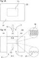
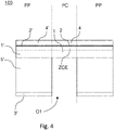
- a first embodiment of the invention illustrated in Figure 1A and 1B relates to a device 100 for measuring a particle beam FS comprising a first part, called the central part PC, a second part, called the peripheral part PP.
- the central part PC comprises means for forming a space charge zone ZCE (in dotted lines on all the figures) intended to be crossed by a beam of particles FS to be measured, charge carriers of a first type and of a second type being generated by said beam FS when the latter crosses the space charge zone ZCE.
- the peripheral part PP comprises means for collecting at least one type of charge carrier from the first type or the second type of charge carriers generated at the level of the space charge zone ZCE.
- the peripheral part PP surrounds the central part PC so that a particle beam FS can pass through the central part PC without passing through the peripheral part PP.
- the device according to the invention makes it possible to measure a beam of particles FS by minimizing the disturbances generated by the measurement on the output beam FS '.
- Such a configuration makes it possible in particular to reduce the amount of radiation absorbed by the device and therefore the number of interactions between material radiation likely to disturb the measurement or degrade the measurement device.
- the measuring device 100 comprises a front face F and a rear face B, the front face F being parallel to the rear face B, and in that an orifice O1 is formed at the level of the face rear B, in a region of the central part PC so that the thickness of said region of the central part PC along an axis normal to the front face F is less than the thickness of the peripheral part PP along said normal axis.
- the orifice O1 can be circular, rectangular or even square. More generally, it can take the form of any polygon.
- the size of the orifice O1 is determined by the size of the beam to be measured. Preferably, the width of the beam is less than the width of the orifice O1.
- the width of the central region can therefore vary from a micron to ten centimeters.
- the entire central part PC is opposite the orifice O1.
- the area of the central part PC is equal to the area of a section of the orifice O1.
- At least one interface opposite the orifice O1 arranged in the rear face B is structured so as to favor the absorption, transmission or reflection of one or more wavelengths.
- This is in particular due to the fact that the ST structuring thus created will favor the harvesting of certain photons (in the case of UV radiation in particular) and therefore the absorption of radiation whose wavelength corresponds to said photons.
- the dimensions of the structures are generally of the same order of magnitude as the dimensions of the wavelength that it is sought to target, that is to say of the order of a few hundred nanometers, for example 200 to 300 nm.
- the device 100 can therefore, in addition to detection, help to filter the incident FS beam. It is therefore possible to obtain a detection device 100 which reads the intensity of the beam FS over a given length for which the absorption coefficient is high, for example greater than or equal to 90%, while absorbing little one or more other wavelengths for which the absorption coefficient is low, for example less than or equal to 10%.
- metal BI balls for example gold, aluminum BI balls
- the BI beads are distributed in a periodic structure so as to form a plasmon network. As the FS beam passes, electromagnetic resonances will occur at the level of the periodic structure thus formed, making it possible to increase the absorption coefficient of the material comprising said balls BI (and therefore of the device 100) for one or more lengths of selected wave.
- the wavelengths affected by the periodic structure are a function of the geometric parameters of said structure, in particular the size of the balls BI and the distance between the balls in the three dimensions of space.
- the central part PC is centered with respect to the whole of the device 100.
- the central part PC and / or the peripheral part PP of the component can be made, at least in part, from a large-gap semiconductor material , for example silicon carbide, diamond or a semiconductor alloy composed of elements from column III-V or II-VI.
- a large-gap semiconductor material for example silicon carbide, diamond or a semiconductor alloy composed of elements from column III-V or II-VI.
- the semiconductor is diamond
- p doping can be obtained by implantation of boron atoms and n doping by implantation of phosphorus atoms.
- the p doping can be by implantation of boron atoms and the n doping by implantation of nitrogen atoms.
- the space charge zone ZCE of the central part PC is only located in the region of the central part PC opposite the orifice O1.
- the space charge zone ZCE of the central part PC extends beyond the region of the central part PC opposite the orifice O1.
- the central part PC comprises a first layer 1 of a semiconductor material; and a second layer 2 of a conductive material covering the first layer 1.
- the ZCE charge space zone is formed by the Schottky diode formed by the first layer 1 and the second layer 2, l orifice O1 being formed in the first layer 1.
- the orifice O1 formed in the first layer 1 of the central part PC can be produced by an engraving technique of the RIE type.
- the peripheral part PP comprises a third layer 3 'of a conductive material; a first layer 1 'of a semiconductor material covering the third layer 3' and arranged in continuity with the first layer 1 of the central part PC; and a second layer 2 ′ of a conductive material covering the first layer 1 and arranged in continuity with the second layer 2 of the central part PC.
- the ZCE space charge zone is formed by the Schottky diode constituted by the first layer 1 of a conductive material and the second layer 2 of a semiconductor material.
- the ZCE space charge area is therefore located on the central PC part but also on the peripheral PP part.
- the third layer 3 'of a conductive material ensures the collection of a first type of charge carriers generated in the charge space charge zone ZCE while the first layer 2.2' made of a material conductor, collects a second type of charge carrier generated in the ZCE space charge zone.
- the second layer 2.2 ′ and the third layer 3.3 ′ may consist of a metal such as copper, zinc or gold or alternatively of monolayer or multilayer graphene.
- Nickel, aluminum, titanium or tungsten can also be used. More generally, any conductive material adapted to the manufacturing or operating conditions of the device can be chosen.
- the material used for the second layer 2.2 ′ may be different from the material used for the third layer 3.3 ′.
- the materials used for the third layer 3 ′ can be chosen so as to obtain ohmic contact between the third layer 3 ′ and the first layer 1 ′ of the peripheral part PP.
- the doping level of the first layer 1 of the central part PC is identical to the doping level of the first layer 1 ′ of the peripheral part.
- the manufacturing process is thereby facilitated because it requires only one level of doping.
- the doping level of the first layer 1 of the central part PC is lower than the doping level of the first layer 1 'of the peripheral part. This configuration ensures a better distribution of the electric field and therefore the use of higher voltages for the polarization of the detector.
- the first layer 1.1 ′ has a thickness of between 500 nm and 50 microns.
- the second layer 2, 2 ′ has a thickness of between 50 nm and 200 nm, preferably substantially equal to 100 nm.
- the central part PC comprises a first layer 1 of a semiconductor material doped in a first type of doping; a second layer 2 of a semiconductor material doped in a second type of doping opposite to the first type of doping, said second layer 2 covering the first layer 1; and a fourth layer 4 of a conductive material, said fourth layer 4 covering the second layer 2.
- the charge space zone ZCE is formed by the PN diode formed by the first layer 1 and the second layer 2, the orifice O1 being formed in the first layer 1.
- the orifice O1 formed in the first layer 1 of the central part PC can be produced by an etching technique of the RIE type.
- the peripheral part PP comprises a third layer 3 'of a conductive material; a first layer 1 'of a semiconductor material doped in a first type of doping covering the third layer 3' and arranged in continuity with the first layer 1 of the central part PC; a second layer 2 'of a semiconductor material doped in a second type of doping opposite to the first type of doping covering the first layer 1', said second layer 2 'being arranged in continuity with the second layer 2 of the part central PC; and a fourth layer 4 'of a conductive material, said fourth layer 4' covering the second layer 2 ', said fourth layer 4' being arranged in continuity with the fourth layer 4 of the PC part.
- the doping of the first layer 1,1 ' is of type n
- the doping of the second layer 2,2' is of type p.
- the space load area ZCE is formed by the PN diode constituted by the first layer 1,1 'of a semiconductor material doped in a first type of doping and the second layer 2,2' of a semiconductor material doped in a second type doping opposite to the first type of doping.
- the ZCE load space zone is therefore located on the central PC part but also on the peripheral PP part.
- the third layer 3 ′ of the peripheral part collects a first type of charge carriers generated in the space charge zone ZCE while the fourth layer 4,4 ′, made of a conductive material, collects a second type of charge carrier generated in the ZCE space charge zone.
- the third layer 3 ′ and the fourth layer 4,4 ′ can be constituted by a metal such as copper, zinc or gold or even by mono or multilayer graphene. Nickel, aluminum, titanium or tungsten can also be used. More generally, any conductive material suitable for the manufacturing or operating conditions of the device can be chosen.
- the material used for the third layer 3 ′ may be different from the material used for the fourth layer 4,4 ′.
- the materials used for the third layer 3 'can be chosen so as to obtain an ohmic contact between the third layer 3' and the first layer 1 'of the peripheral part PP.
- the materials used for the fourth layer 4,4 'can be chosen so as to obtain an ohmic contact between the fourth layer 4,4' and the second layer 2,2 '.
- the doping level of the first layer 1 of the central part PC is identical to the doping level of the first layer 1 ′ of the peripheral part PP.
- the doping level of the second layer 2 of the central part PC is identical to the doping level of the second layer 2 'of the peripheral part. As explained above, the manufacturing process is made easier because it requires only one level of doping.
- the doping of the first layer 1,1 ' is of type n and the doping of the second layer 2,2' is of type p.
- the doping level of the first layer 1.1 ′ is between 5.10 14 and 5.10 19 atoms per cm 3 , of preferably substantially equal to 5.10 15 atoms per cm 3 .
- the doping level of the second layer 2.2 ′ is between 1.10 16 and 5.10 19 atoms per cm 3 , preferably substantially equal to 1.10 19 atoms per cm 3 .
- the doping level of the first layer 1 of the central part PC is lower than the doping level of the first layer 1 'of the peripheral part.
- the doping level of the second layer 2 of the central part PC is lower than the doping level of the second layer 2 'of the peripheral part.
- the peripheral part PP comprises a fifth layer 5 ′ of a semiconductor material doped in a first type of doping, the doping level of the fifth layer 5 ′ of the peripheral part PP being higher than the doping level of the first layer 1 'of the peripheral part PP, the fifth layer 5' being located between the third layer 3 'and the first layer 1' of the peripheral part PP.
- the PIN diode formed between the fifth layer 5 'of the peripheral part, the first layer 1.1' and the first layer 2.2 ' allows better recovery of the charges generated in the central part PC by the FS beam of particles to be detected.
- the central part PC of the device is preferably identical to the central part of the device according to the second embodiment.
- the fifth layer 5 ′ of the peripheral part PP can for example be obtained by etching the orifice O1 in a layer of a semiconductor material doped in a first type of doping, said layer being present in the central part PC and the peripheral part PP before etching and being etched throughout its thickness in order to form the orifice O1.
- the etching can be carried out by a dry technique of the RIE type or even a wet technique.
- the doping of the first layer 1,1 'and of the fifth layer 5' of the peripheral part PP is of n type and the doping of the second layer 2,2 'is of p type.
- the doping level of the fifth layer 5 ′ is between 1.10 16 and 1.10 19 atoms per cm 3 , preferably substantially equal to 110 18 atoms per cm 3 .
- the doping level of the first layer 1.1 ′ is between 5.10 14 and 5.10 19 atoms per cm 3 , preferably substantially equal to 5.10 15 atoms per cm 3 .
- the doping level of the second layer 2.2 ′ is between 1.10 16 and 5.10 19 atoms per cm 3 , preferably substantially equal to 1.10 19 atoms per cm 3 .
- the first layer 1.1 ′ has a thickness of between 500 nm and 50 microns; the second layer 2, 2 ′ has a thickness of between 50 and 200 nm, preferably substantially equal to 100 nm; and the fifth layer has a thickness between 250 and 350 microns, preferably substantially equal to 300 microns.
- the central part PC comprises a first layer 1 of a semiconductor material doped in a first type of doping and a second layer 2 of a semiconductor material doped in a second type of doping opposite to the first type of doping, said second layer 2 covering the first layer 1.
- the central part is therefore devoid of this electrode embodiment.
- the space charge area is also produced by the PN diode constituted by the first layer 1,1 'of a semiconductor material doped in a first type of doping and the second layer 2,2 'of a semiconductor material doped in a second type of doping opposite to the first type of doping.
- the charge carriers are recovered only at the level of the peripheral part by the third layer 3 'and fourth layer 4' of the peripheral part PP.
- the beam only crosses the first layer 1 and the second layer 2 of the central part at the level of which the load space zone is formed.
- the fourth layer 4 ′ is only found on the peripheral part and therefore forms a second orifice 02.
- the space charge zone ZCE is present both in the central part PC and the peripheral part PP of the device.
- the peripheral part PP comprises a third layer 3 'of a conductive material; a first layer 1 ′ of a semiconductor material doped in a first type of doping covering the third layer 3 ′ and arranged in continuity with the first layer 1 of the central part PC ,; a sixth layer 6 'of an oxide covering the first layer 1'; and a fourth layer 4 'of a conductive material covering the sixth layer 6'.
- the second layer 2,2 ′ being present only in the central part PC of the device, the space charge area ZCE is also restricted to the central part PC of the device 100.
- the fourth layer 4, 4 ′ forms a step between the peripheral part PP and the central part PC covering a lateral surface of the sixth layer 6 so as to ensure continuity between the fourth layer 4 of the central part PC and the fourth layer 4 ′ of the peripheral part PP.
- the sixth layer 6 ′ is only found on the peripheral part and therefore forms a second orifice 02.
- the fourth layer 4 ′ of the central part PC covers the entire central part PC through which the beam to be measured passes. It may be advantageous in certain situations to reduce this absorption phenomenon. To this end, in a sixth embodiment illustrated in figure 7 , the fourth layer 4 ′ of the central part covers only a part only of the central part PC.
- the MIS (Semiconductor Insulating Metal) structure formed at the peripheral part PP of the device formed by the first layer of the peripheral part 1 ′, the sixth layer of the peripheral part 6 ′ and by the fourth layer 4 ′ of the peripheral part can disturb the measurement by inducing in particular capacitive effects.
- the second layer 2 'of the peripheral part only partially covers the first layer 1' of the peripheral part while ensuring continuity with the second layer 2 of the central part PC.
- the second layer 2,2 ′ is present throughout the central part PC of the device as well as in an area of the peripheral part PP.
- the presence of the second layer 2 ′ over a larger area than the central part PC limits the formation of the MIS structure previously mentioned. This reduces the capacitive phenomena between the first layer of the peripheral part 1 ', the sixth layer of the peripheral part 6' and by the fourth layer 4 'of the peripheral part.
- the first orifice O1 is defined by a side wall PL and by a bottom FD and a layer of an oxide 7 covers the side wall PL and the bottom FD of the first orifice.
- the part of the orifice O1 formed in the fifth 5.5 ′ and / or the first layer 1.1 ′ can be obtained by an etching technique, for example by RIE.
- This manufacturing method has the disadvantage of producing dangling bonds on the surfaces left free after etching. These dangling connections can alter the electrical properties of the material near said free surfaces.
- the presence of the oxide layer 7 neutralizes the pendant connections resulting from the manufacture of the orifice O1 and thus eliminates the electrical disturbances that these pendant connections are liable to generate.
- the oxide layer 7 may be present on the entire side wall PL or else only on the side wall PL formed by the material of the fifth 5.5 'and / or the first layer 1.1', mainly concerned by the problem of dangling bonds.
Claims (14)
- Messvorrichtung (100) eines Partikelstrahls, umfassend einen ersten Teil, bezeichnet als zentraler Teil (PC), einen zweiten Teil, bezeichnet als umlaufender Teil (PP), eine vordere Seite (F) und eine hintere Seite (B), wobei die vordere Seite (F) parallel zur hinteren Seite (B) ist;- wobei der zentrale Teil (PC) Mittel zum Formen einer Raumchargen-Zone (ZCE) umfasst, die dazu bestimmt ist, von einem zu messenden Partikelstrahl (FS) durchquert zu sein, wobei Chargenträger eines ersten Typs und eines zweiten Typs von dem genannten Strahl (FS) erzeugt sind, wenn Letzterer die Raumchargen-Zone (ZCE) durchquert;- wobei der umlaufende Teil (PP) Mittel zum Erfassen wenigstens eines Chargenträgertyps aus dem ersten Typ oder dem zweiten Typ des Chargenträgers umfasst, die an der Raumchargen-Zone (ZCE) erzeugt sind;wobei der umlaufende Teil (PP) den zentralen Teil (PC) derart umgibt, dass ein Partikelstrahl (FS) den zentralen Teil (PC) ohne Durchqueren des umlaufenden Teils (PP) durchqueren kann, wobei die Messvorrichtung dadurch gekennzeichnet ist, dass eine Öffnung (O1) an der hinteren Seite (B) in einer Region des zentralen Teils (PC) derart angeordnet ist, dass die Dicke der genannten Region des zentralen Teils (PC) gemäß einer normalen Achse an der vorderen Seite (F) geringer ist als die Dicke des umlaufenden Teils (PP) gemäß der genannten normalen Achse.
- Messvorrichtung (100) gemäß dem voranstehenden Anspruch, dadurch gekennzeichnet, dass wenigstens eine Schnittstelle gegenüber der Öffnung (O1), die in der hinteren (B) oder der vorderen Seite derart strukturiert ist, dass die Absorption, die Übertragung oder das Reflektieren einer oder mehrerer Wellenlänge(n) begünstigt ist.
- Messvorrichtung (100) gemäß einem der voranstehenden Ansprüche, dadurch gekennzeichnet, dass Metallkugeln (BI) in dem zentralen Teil (PC) oder gemäß der Optimierung der Ernte der Chargenträger, d. h. häufig nicht weit von der ZCE vorhanden ist, wobei die genannten Kugeln (BI) gemäß einer periodischen Struktur derart verteilt sind, dass ein plasmonisches Netz geformt ist.
- Messvorrichtung (100) gemäß einem der voranstehenden Ansprüche, dadurch gekennzeichnet, dass der zentrale Teil (PC) aus einem Halbleitermaterial mit großem Gap realisiert ist.
- Messvorrichtung (100) gemäß dem voranstehenden Anspruch, dadurch gekennzeichnet, dass der Halbleiter das Siliziumkarbid ist.
- Messvorrichtung (100) gemäß einem der voranstehenden Ansprüche, dadurch gekennzeichnet, dass die Chargenraum-Zone (ZCE) mithilfe einer Schottky-Diode, einer PN-Diode oder einer PIN-Diode geformt ist.
- Messvorrichtung (100) gemäß einem der voranstehenden Ansprüche, dadurch gekennzeichnet, dass die Raumchargen-Zone (ZCE) des zentralen Teils (PC) ausschließlich in der Region des zentralen Teils (PC) gegenüber der Öffnung (O1) angeordnet ist.
- Messvorrichtung (100) gemäß einem der Ansprüche 1 bis 4, dadurch gekennzeichnet, dass die Raumchargen-Zone (ZCE) des zentralen Teils (PC) sich über die Region des zentralen Teils (PC) gegenüber der Öffnung (O1) hinweg erstreckt.
- Messvorrichtung (100) gemäß einem der Ansprüche 1 bis 4, dadurch gekennzeichnet, dass der zentrale Teil (PC) umfasst:- eine erste Schicht (1) eines Halbleiter-Materials;- eine zweite Schicht (2) eines leitenden Materials, die die erste Schicht (1) überdeckt;wobei die Chargenraum-Zone (ZCE) von der Schottky-Diode geformt ist, die von der ersten Schicht (1) und der zweiten Schicht (2) geformt ist, wobei die Öffnung (O1) in der ersten Schicht (1) ausgespart ist.
- Messvorrichtung (100) gemäß dem voranstehenden Anspruch, dadurch gekennzeichnet, dass der umlaufende Teil (PP) umfasst:- eine dritte Schicht (3') eines leitenden Materials;- eine erste Schicht (1') eines Halbleitermaterials, die die dritte Schicht (3') abdeckt und in Fortsetzung der ersten Schicht (1) des zentralen Teils (PC) angeordnet ist;- eine zweite Schicht (2') eines leitenden Materials, die die erste Schicht (1) abdeckt und in Fortsetzung der zweiten Schicht (2) des zentralen Teils (PC) angeordnet ist;wobei die dritte Schicht (3') eines leitenden Materials das Erfassen eines ersten Typs von Chargenträgern gewährleistet, die in der Chargenraum-Zone (ZCE) erzeugt sind.
- Messvorrichtung (100) gemäß einem der Ansprüche 1 bis 4, dadurch gekennzeichnet, dass der zentrale Teil (PC) umfasst:- eine erste Schicht (1) eines gedopten Halbleiter-Materials in einem ersten Dopingtyp;- eine zweite Schicht (2) eines gedopten Halbleitermaterials in einem zweiten Dopingtyp, der dem ersten Dopingtyp entgegengesetzt ist, wobei die genannte zweite Schicht (2) die erste Schicht (1) abdeckt;- eine vierte Schicht (4) eines leitenden Materials, wobei die genannte vierte Schicht (4) die zweite Schicht (2) abdeckt;wobei die Chargenraum-Zone (ZCE) durch die PN-Diode geformt ist, die von der ersten Schicht (1) und der zweiten Schicht (2) geformt ist, wobei die Öffnung (O1) in der ersten Schicht (1) ausgespart ist.
- Messvorrichtung (100) gemäß dem voranstehenden Anspruch, dadurch gekennzeichnet, dass der umlaufende Teil umfasst:- eine dritte Schicht (3') aus einem leitenden Material;- eine erste Schicht (1') aus einem gedopten Halbleiter-Material aus einem ersten Dopingtyp, die die dritte Schicht (3') abdeckt und in Fortführung der ersten Schicht (1) des zentralen Teils (PC) angeordnet ist;- eine zweite Schicht (2') eines gedopten Halbleitermaterials aus einem zweiten Dopingtyp, der dem ersten Dopingtyp entgegengesetzt ist, der die erste Schicht (1') abdeckt, wobei die genannte zweite Schicht (2') in Fortführung der zweiten Schicht (2) des zentralen Teils (PC) angeordnet ist;- eine vierte Schicht (4') eines leitenden Materials, wobei die genannte vierte Schicht (4') die zweite Schicht (2') abdeckt, wobei die genannte vierte Schicht (4') in Fortführung der vierten Schicht (4) des zentralen Teils (PC) angeordnet ist;wobei die dritte Schicht (3) eines leitenden Materials das Erfassen eines ersten Typs von Chargenträgern, die in der Chargenraum-Zone (ZCE) erzeugt sind, gewährleistet.
- Messvorrichtung (100) gemäß Anspruch 9, dadurch gekennzeichnet, dass der umlaufende Teil (PP) umfasst:- eine dritte Schicht (3') eines leitenden Materials;- eine erste Schicht (1') eines gedopten Halbleiter-Materials aus einem ersten Dopingtyp, der die dritte Schicht (3') abdeckt und in Fortführung der ersten Schicht (1) des ersten zentralen Teils (PC) angeordnet ist, wobei die erste Schicht (1) des zentralen Teils (PC) und des umlaufenden Teils (PP) dasselbe Dopingniveau aufweist;- eine sechste Schicht (6) eines Sauerstoffs, die die erste Schicht (1) abdeckt;- eine vierte Schicht (4') eines leitenden Materials, die die sechste Schicht (6) abdeckt;wobei die vierte Schicht (4, 4') eine Stufe zwischen dem umlaufenden Teil (PP) und dem zentralen Teil (PC) formt, die eine seitliche Oberfläche der sechsten Schicht (6) derart bildet, dass eine Fortführung zwischen der vierten Schicht (4) des zentralen Teils (PC) und der vierten Schicht (4') des umlaufenden Teils (PP) gebildet ist.
- Vorrichtung gemäß einem der zwei voranstehenden Ansprüche, dadurch gekennzeichnet, dass der umlaufende Teil (PP) eine fünfte Schicht (5') eines gedopten Halbleiter-Materials aus einem ersten Dopingtyp umfasst, wobei das Dopingniveau der fünften Schicht (5') höher ist als das Dopingniveau der ersten Schicht (1'), wobei die vierte Schicht zwischen der dritten Schicht (3') und der ersten Schicht (1') des umlaufenden Teils (PP) angeordnet ist.
Applications Claiming Priority (2)
| Application Number | Priority Date | Filing Date | Title |
|---|---|---|---|
| FR1654382A FR3051557A1 (fr) | 2016-05-17 | 2016-05-17 | Detecteur de particules realise dans un materiau semi-conducteur |
| PCT/EP2017/061637 WO2017198630A1 (fr) | 2016-05-17 | 2017-05-15 | Detecteur de particules realise dans un materiau semi-conducteur |
Publications (2)
| Publication Number | Publication Date |
|---|---|
| EP3458878A1 EP3458878A1 (de) | 2019-03-27 |
| EP3458878B1 true EP3458878B1 (de) | 2020-07-01 |
Family
ID=57184536
Family Applications (1)
| Application Number | Title | Priority Date | Filing Date |
|---|---|---|---|
| EP17723993.6A Active EP3458878B1 (de) | 2016-05-17 | 2017-05-15 | Aus einem halbleitermaterial hergestellter partikeldetektor |
Country Status (6)
| Country | Link |
|---|---|
| US (1) | US10591620B2 (de) |
| EP (1) | EP3458878B1 (de) |
| CA (1) | CA3024395C (de) |
| DK (1) | DK3458878T3 (de) |
| FR (1) | FR3051557A1 (de) |
| WO (1) | WO2017198630A1 (de) |
Cited By (1)
| Publication number | Priority date | Publication date | Assignee | Title |
|---|---|---|---|---|
| FR3118300A1 (fr) * | 2020-12-23 | 2022-06-24 | Université D'aix Marseille | Detecteur de particules comprenant une region poreuse realisee dans un materiau semi-conducteur et procede de fabrication associe |
Families Citing this family (4)
| Publication number | Priority date | Publication date | Assignee | Title |
|---|---|---|---|---|
| FR3099293A1 (fr) * | 2019-07-26 | 2021-01-29 | Université D'aix Marseille | Dispositif monobloc de détection de particules à matériau semi-conducteur |
| FR3100343B1 (fr) | 2019-09-02 | 2021-08-27 | Centre Nat Rech Scient | Dosimetre |
| FR3112400B1 (fr) | 2020-07-10 | 2022-06-17 | Univ Aix Marseille | Procédé de fabrication d’une tête d’irradiation d’une cible avec un faisceau de particules ionisantes |
| FR3119246B1 (fr) | 2021-01-27 | 2023-02-24 | Centre Nat Rech Scient | Procede de fabrication d'un detecteur des flux d'un premier et d'un deuxieme rayonnements ionisants |
Family Cites Families (7)
| Publication number | Priority date | Publication date | Assignee | Title |
|---|---|---|---|---|
| EP0241237B1 (de) * | 1986-04-11 | 1992-12-23 | AT&T Corp. | Strahlungsdetektoranordnung |
| DE69622455T2 (de) * | 1995-04-07 | 2002-11-07 | Rikagaku Kenkyusho | Monitor und Verfahren zur Bestimmung der Lage eines Röntgenstrahls |
| US7253434B2 (en) * | 2002-10-29 | 2007-08-07 | President And Fellows Of Harvard College | Suspended carbon nanotube field effect transistor |
| JP5096747B2 (ja) * | 2006-03-02 | 2012-12-12 | 株式会社神戸製鋼所 | ビーム検出部材およびそれを用いたビーム検出器 |
| US7586167B2 (en) * | 2006-05-05 | 2009-09-08 | Virgin Islands Microsystems, Inc. | Detecting plasmons using a metallurgical junction |
| US7816651B2 (en) * | 2007-09-27 | 2010-10-19 | Varian Medical Systems, Inc. | High detective quantum efficiency X-ray detectors |
| US9515211B2 (en) * | 2013-07-26 | 2016-12-06 | University Of South Carolina | Schottky barrier detection devices having a 4H-SiC n-type epitaxial layer |
-
2016
- 2016-05-17 FR FR1654382A patent/FR3051557A1/fr active Pending
-
2017
- 2017-05-15 DK DK17723993.6T patent/DK3458878T3/da active
- 2017-05-15 CA CA3024395A patent/CA3024395C/fr active Active
- 2017-05-15 WO PCT/EP2017/061637 patent/WO2017198630A1/fr unknown
- 2017-05-15 EP EP17723993.6A patent/EP3458878B1/de active Active
- 2017-05-15 US US16/302,426 patent/US10591620B2/en active Active
Non-Patent Citations (1)
| Title |
|---|
| None * |
Cited By (2)
| Publication number | Priority date | Publication date | Assignee | Title |
|---|---|---|---|---|
| FR3118300A1 (fr) * | 2020-12-23 | 2022-06-24 | Université D'aix Marseille | Detecteur de particules comprenant une region poreuse realisee dans un materiau semi-conducteur et procede de fabrication associe |
| WO2022136516A1 (fr) * | 2020-12-23 | 2022-06-30 | Université D'aix Marseille | Detecteur de particules comprenant une region poreuse realisee dans un materiau semi-conducteur et procede de fabrication associe |
Also Published As
| Publication number | Publication date |
|---|---|
| US10591620B2 (en) | 2020-03-17 |
| CA3024395C (fr) | 2024-03-26 |
| WO2017198630A1 (fr) | 2017-11-23 |
| DK3458878T3 (da) | 2020-09-28 |
| US20190277983A1 (en) | 2019-09-12 |
| EP3458878A1 (de) | 2019-03-27 |
| FR3051557A1 (fr) | 2017-11-24 |
| CA3024395A1 (fr) | 2017-11-23 |
Similar Documents
| Publication | Publication Date | Title |
|---|---|---|
| EP3458878B1 (de) | Aus einem halbleitermaterial hergestellter partikeldetektor | |
| EP2752893B1 (de) | Halbleiterstruktur vom Typ Lawinen-Fotodiode, und Herstellungsverfahren einer solchen Struktur | |
| EP2865017B1 (de) | Halbleiterstruktur mit absorbierendem bereich in einem fokusierenden resonator | |
| FR2970599A1 (fr) | Photodetecteur optimise par une texturation metallique agencee en face arriere | |
| EP2339640A1 (de) | Photodetektor mit Plasmonstruktur | |
| EP2786426B1 (de) | Halbleiterstruktur zur aufnahme von elektromagnetischer strahlung, halbleiterbauelement und verfahren zur herstellung einer solchen halbleiterstruktur | |
| EP2937902B1 (de) | Matrix aus cdhgte-fotodioden | |
| WO2012080989A2 (fr) | Dispositif de photodetection | |
| EP2750203B1 (de) | Halbleiterstruktur vom Typ Lawinen-Fotodiode mit geringer Ansprechzeit, und Herstellungsverfahren einer solchen Fotodiode | |
| EP2276072B1 (de) | Photodetektorelement | |
| EP2939275B1 (de) | Halbleiterstruktur mit lawinenphotodiode mit hohem rauschabstand und verfahren zur herstellung solch einer photodiode | |
| EP2432033A2 (de) | Bispektraler Mehrschichtdetektor mit Fotodioden | |
| EP2801115B1 (de) | Fotodetektor | |
| EP3703138B1 (de) | Struktur zur erkennung einer elektromagnetischen strahlung mit hoher absorptionseffizienz, und herstellungsverfahren einer solchen struktur | |
| EP3208854A1 (de) | Photodiodenstruktur, bestandteil und herstellungsverfahren einer solchen photodiodenstruktur | |
| WO2022136516A1 (fr) | Detecteur de particules comprenant une region poreuse realisee dans un materiau semi-conducteur et procede de fabrication associe | |
| FR3032304A1 (fr) | Structure semiconductrice a deux cavites resonantes couplees optiquement et procede de fabrication d'une telle structure | |
| WO2013030482A1 (fr) | Dispositif reflecteur pour face arriere de dispositifs optiques | |
| EP2382672A1 (de) | Verfahren zur herstellung einer photodiode und entsprechende photodiode und elektromagnetischer strahlungsdetektor |
Legal Events
| Date | Code | Title | Description |
|---|---|---|---|
| STAA | Information on the status of an ep patent application or granted ep patent |
Free format text: STATUS: UNKNOWN |
|
| STAA | Information on the status of an ep patent application or granted ep patent |
Free format text: STATUS: THE INTERNATIONAL PUBLICATION HAS BEEN MADE |
|
| PUAI | Public reference made under article 153(3) epc to a published international application that has entered the european phase |
Free format text: ORIGINAL CODE: 0009012 |
|
| STAA | Information on the status of an ep patent application or granted ep patent |
Free format text: STATUS: REQUEST FOR EXAMINATION WAS MADE |
|
| 17P | Request for examination filed |
Effective date: 20181116 |
|
| AK | Designated contracting states |
Kind code of ref document: A1 Designated state(s): AL AT BE BG CH CY CZ DE DK EE ES FI FR GB GR HR HU IE IS IT LI LT LU LV MC MK MT NL NO PL PT RO RS SE SI SK SM TR |
|
| AX | Request for extension of the european patent |
Extension state: BA ME |
|
| DAV | Request for validation of the european patent (deleted) | ||
| DAX | Request for extension of the european patent (deleted) | ||
| GRAP | Despatch of communication of intention to grant a patent |
Free format text: ORIGINAL CODE: EPIDOSNIGR1 |
|
| STAA | Information on the status of an ep patent application or granted ep patent |
Free format text: STATUS: GRANT OF PATENT IS INTENDED |
|
| INTG | Intention to grant announced |
Effective date: 20191212 |
|
| RIN1 | Information on inventor provided before grant (corrected) |
Inventor name: OTTAVIANI, LAURENT Inventor name: VERVISCH, WILFRIED VIVIAN ROLAND Inventor name: BIONDO, STEPHANE Inventor name: HURTADO EP VERVISCH, VANESSA LAURENCE JILL |
|
| GRAS | Grant fee paid |
Free format text: ORIGINAL CODE: EPIDOSNIGR3 |
|
| GRAA | (expected) grant |
Free format text: ORIGINAL CODE: 0009210 |
|
| STAA | Information on the status of an ep patent application or granted ep patent |
Free format text: STATUS: THE PATENT HAS BEEN GRANTED |
|
| AK | Designated contracting states |
Kind code of ref document: B1 Designated state(s): AL AT BE BG CH CY CZ DE DK EE ES FI FR GB GR HR HU IE IS IT LI LT LU LV MC MK MT NL NO PL PT RO RS SE SI SK SM TR |
|
| REG | Reference to a national code |
Ref country code: CH Ref legal event code: EP Ref country code: AT Ref legal event code: REF Ref document number: 1286682 Country of ref document: AT Kind code of ref document: T Effective date: 20200715 |
|
| REG | Reference to a national code |
Ref country code: IE Ref legal event code: FG4D Free format text: LANGUAGE OF EP DOCUMENT: FRENCH |
|
| REG | Reference to a national code |
Ref country code: DE Ref legal event code: R096 Ref document number: 602017019032 Country of ref document: DE |
|
| REG | Reference to a national code |
Ref country code: DK Ref legal event code: T3 Effective date: 20200924 |
|
| REG | Reference to a national code |
Ref country code: NL Ref legal event code: FP |
|
| REG | Reference to a national code |
Ref country code: SE Ref legal event code: TRGR |
|
| REG | Reference to a national code |
Ref country code: CH Ref legal event code: NV Representative=s name: VALIPAT S.A. C/O BOVARD SA NEUCHATEL, CH |
|
| REG | Reference to a national code |
Ref country code: NO Ref legal event code: T2 Effective date: 20200701 |
|
| REG | Reference to a national code |
Ref country code: LT Ref legal event code: MG4D |
|
| PG25 | Lapsed in a contracting state [announced via postgrant information from national office to epo] |
Ref country code: BG Free format text: LAPSE BECAUSE OF FAILURE TO SUBMIT A TRANSLATION OF THE DESCRIPTION OR TO PAY THE FEE WITHIN THE PRESCRIBED TIME-LIMIT Effective date: 20201001 |
|
| PG25 | Lapsed in a contracting state [announced via postgrant information from national office to epo] |
Ref country code: ES Free format text: LAPSE BECAUSE OF FAILURE TO SUBMIT A TRANSLATION OF THE DESCRIPTION OR TO PAY THE FEE WITHIN THE PRESCRIBED TIME-LIMIT Effective date: 20200701 Ref country code: PT Free format text: LAPSE BECAUSE OF FAILURE TO SUBMIT A TRANSLATION OF THE DESCRIPTION OR TO PAY THE FEE WITHIN THE PRESCRIBED TIME-LIMIT Effective date: 20201102 Ref country code: CZ Free format text: LAPSE BECAUSE OF FAILURE TO SUBMIT A TRANSLATION OF THE DESCRIPTION OR TO PAY THE FEE WITHIN THE PRESCRIBED TIME-LIMIT Effective date: 20200701 Ref country code: LT Free format text: LAPSE BECAUSE OF FAILURE TO SUBMIT A TRANSLATION OF THE DESCRIPTION OR TO PAY THE FEE WITHIN THE PRESCRIBED TIME-LIMIT Effective date: 20200701 Ref country code: HR Free format text: LAPSE BECAUSE OF FAILURE TO SUBMIT A TRANSLATION OF THE DESCRIPTION OR TO PAY THE FEE WITHIN THE PRESCRIBED TIME-LIMIT Effective date: 20200701 Ref country code: GR Free format text: LAPSE BECAUSE OF FAILURE TO SUBMIT A TRANSLATION OF THE DESCRIPTION OR TO PAY THE FEE WITHIN THE PRESCRIBED TIME-LIMIT Effective date: 20201002 Ref country code: FI Free format text: LAPSE BECAUSE OF FAILURE TO SUBMIT A TRANSLATION OF THE DESCRIPTION OR TO PAY THE FEE WITHIN THE PRESCRIBED TIME-LIMIT Effective date: 20200701 |
|
| PG25 | Lapsed in a contracting state [announced via postgrant information from national office to epo] |
Ref country code: RS Free format text: LAPSE BECAUSE OF FAILURE TO SUBMIT A TRANSLATION OF THE DESCRIPTION OR TO PAY THE FEE WITHIN THE PRESCRIBED TIME-LIMIT Effective date: 20200701 Ref country code: PL Free format text: LAPSE BECAUSE OF FAILURE TO SUBMIT A TRANSLATION OF THE DESCRIPTION OR TO PAY THE FEE WITHIN THE PRESCRIBED TIME-LIMIT Effective date: 20200701 Ref country code: LV Free format text: LAPSE BECAUSE OF FAILURE TO SUBMIT A TRANSLATION OF THE DESCRIPTION OR TO PAY THE FEE WITHIN THE PRESCRIBED TIME-LIMIT Effective date: 20200701 Ref country code: IS Free format text: LAPSE BECAUSE OF FAILURE TO SUBMIT A TRANSLATION OF THE DESCRIPTION OR TO PAY THE FEE WITHIN THE PRESCRIBED TIME-LIMIT Effective date: 20201101 |
|
| REG | Reference to a national code |
Ref country code: DE Ref legal event code: R097 Ref document number: 602017019032 Country of ref document: DE |
|
| PG25 | Lapsed in a contracting state [announced via postgrant information from national office to epo] |
Ref country code: RO Free format text: LAPSE BECAUSE OF FAILURE TO SUBMIT A TRANSLATION OF THE DESCRIPTION OR TO PAY THE FEE WITHIN THE PRESCRIBED TIME-LIMIT Effective date: 20200701 Ref country code: SM Free format text: LAPSE BECAUSE OF FAILURE TO SUBMIT A TRANSLATION OF THE DESCRIPTION OR TO PAY THE FEE WITHIN THE PRESCRIBED TIME-LIMIT Effective date: 20200701 Ref country code: EE Free format text: LAPSE BECAUSE OF FAILURE TO SUBMIT A TRANSLATION OF THE DESCRIPTION OR TO PAY THE FEE WITHIN THE PRESCRIBED TIME-LIMIT Effective date: 20200701 |
|
| PLBE | No opposition filed within time limit |
Free format text: ORIGINAL CODE: 0009261 |
|
| STAA | Information on the status of an ep patent application or granted ep patent |
Free format text: STATUS: NO OPPOSITION FILED WITHIN TIME LIMIT |
|
| PG25 | Lapsed in a contracting state [announced via postgrant information from national office to epo] |
Ref country code: AL Free format text: LAPSE BECAUSE OF FAILURE TO SUBMIT A TRANSLATION OF THE DESCRIPTION OR TO PAY THE FEE WITHIN THE PRESCRIBED TIME-LIMIT Effective date: 20200701 |
|
| 26N | No opposition filed |
Effective date: 20210406 |
|
| PG25 | Lapsed in a contracting state [announced via postgrant information from national office to epo] |
Ref country code: SK Free format text: LAPSE BECAUSE OF FAILURE TO SUBMIT A TRANSLATION OF THE DESCRIPTION OR TO PAY THE FEE WITHIN THE PRESCRIBED TIME-LIMIT Effective date: 20200701 |
|
| PG25 | Lapsed in a contracting state [announced via postgrant information from national office to epo] |
Ref country code: SI Free format text: LAPSE BECAUSE OF FAILURE TO SUBMIT A TRANSLATION OF THE DESCRIPTION OR TO PAY THE FEE WITHIN THE PRESCRIBED TIME-LIMIT Effective date: 20200701 |
|
| PG25 | Lapsed in a contracting state [announced via postgrant information from national office to epo] |
Ref country code: LU Free format text: LAPSE BECAUSE OF NON-PAYMENT OF DUE FEES Effective date: 20210515 Ref country code: MC Free format text: LAPSE BECAUSE OF FAILURE TO SUBMIT A TRANSLATION OF THE DESCRIPTION OR TO PAY THE FEE WITHIN THE PRESCRIBED TIME-LIMIT Effective date: 20200701 |
|
| PG25 | Lapsed in a contracting state [announced via postgrant information from national office to epo] |
Ref country code: IE Free format text: LAPSE BECAUSE OF NON-PAYMENT OF DUE FEES Effective date: 20210515 |
|
| PG25 | Lapsed in a contracting state [announced via postgrant information from national office to epo] |
Ref country code: CY Free format text: LAPSE BECAUSE OF FAILURE TO SUBMIT A TRANSLATION OF THE DESCRIPTION OR TO PAY THE FEE WITHIN THE PRESCRIBED TIME-LIMIT Effective date: 20200701 |
|
| P01 | Opt-out of the competence of the unified patent court (upc) registered |
Effective date: 20230530 |
|
| REG | Reference to a national code |
Ref country code: AT Ref legal event code: UEP Ref document number: 1286682 Country of ref document: AT Kind code of ref document: T Effective date: 20200701 |
|
| PG25 | Lapsed in a contracting state [announced via postgrant information from national office to epo] |
Ref country code: HU Free format text: LAPSE BECAUSE OF FAILURE TO SUBMIT A TRANSLATION OF THE DESCRIPTION OR TO PAY THE FEE WITHIN THE PRESCRIBED TIME-LIMIT; INVALID AB INITIO Effective date: 20170515 |
|
| PGFP | Annual fee paid to national office [announced via postgrant information from national office to epo] |
Ref country code: NO Payment date: 20230526 Year of fee payment: 7 Ref country code: NL Payment date: 20230530 Year of fee payment: 7 Ref country code: IT Payment date: 20230526 Year of fee payment: 7 Ref country code: FR Payment date: 20230530 Year of fee payment: 7 Ref country code: DK Payment date: 20230526 Year of fee payment: 7 Ref country code: DE Payment date: 20230526 Year of fee payment: 7 Ref country code: CH Payment date: 20230605 Year of fee payment: 7 |
|
| PGFP | Annual fee paid to national office [announced via postgrant information from national office to epo] |
Ref country code: SE Payment date: 20230526 Year of fee payment: 7 Ref country code: AT Payment date: 20230526 Year of fee payment: 7 |
|
| PGFP | Annual fee paid to national office [announced via postgrant information from national office to epo] |
Ref country code: BE Payment date: 20230530 Year of fee payment: 7 |
|
| PGFP | Annual fee paid to national office [announced via postgrant information from national office to epo] |
Ref country code: GB Payment date: 20230530 Year of fee payment: 7 |
|
| PG25 | Lapsed in a contracting state [announced via postgrant information from national office to epo] |
Ref country code: MK Free format text: LAPSE BECAUSE OF FAILURE TO SUBMIT A TRANSLATION OF THE DESCRIPTION OR TO PAY THE FEE WITHIN THE PRESCRIBED TIME-LIMIT Effective date: 20200701 |