EP3454363A1 - Chip package structure, chip module, and electronic terminal - Google Patents
Chip package structure, chip module, and electronic terminal Download PDFInfo
- Publication number
- EP3454363A1 EP3454363A1 EP17900275.3A EP17900275A EP3454363A1 EP 3454363 A1 EP3454363 A1 EP 3454363A1 EP 17900275 A EP17900275 A EP 17900275A EP 3454363 A1 EP3454363 A1 EP 3454363A1
- Authority
- EP
- European Patent Office
- Prior art keywords
- chip
- substrate
- packaging structure
- electrical connection
- connection structure
- Prior art date
- Legal status (The legal status is an assumption and is not a legal conclusion. Google has not performed a legal analysis and makes no representation as to the accuracy of the status listed.)
- Withdrawn
Links
Images

Classifications
-
- H—ELECTRICITY
- H10—SEMICONDUCTOR DEVICES; ELECTRIC SOLID-STATE DEVICES NOT OTHERWISE PROVIDED FOR
- H10W—GENERIC PACKAGES, INTERCONNECTIONS, CONNECTORS OR OTHER CONSTRUCTIONAL DETAILS OF DEVICES COVERED BY CLASS H10
- H10W74/00—Encapsulations, e.g. protective coatings
- H10W74/10—Encapsulations, e.g. protective coatings characterised by their shape or disposition
- H10W74/111—Encapsulations, e.g. protective coatings characterised by their shape or disposition the semiconductor body being completely enclosed
- H10W74/114—Encapsulations, e.g. protective coatings characterised by their shape or disposition the semiconductor body being completely enclosed by a substrate and the encapsulations
-
- H—ELECTRICITY
- H10—SEMICONDUCTOR DEVICES; ELECTRIC SOLID-STATE DEVICES NOT OTHERWISE PROVIDED FOR
- H10D—INORGANIC ELECTRIC SEMICONDUCTOR DEVICES
- H10D62/00—Semiconductor bodies, or regions thereof, of devices having potential barriers
- H10D62/10—Shapes, relative sizes or dispositions of the regions of the semiconductor bodies; Shapes of the semiconductor bodies
- H10D62/117—Shapes of semiconductor bodies
-
- H—ELECTRICITY
- H10—SEMICONDUCTOR DEVICES; ELECTRIC SOLID-STATE DEVICES NOT OTHERWISE PROVIDED FOR
- H10W—GENERIC PACKAGES, INTERCONNECTIONS, CONNECTORS OR OTHER CONSTRUCTIONAL DETAILS OF DEVICES COVERED BY CLASS H10
- H10W70/00—Package substrates; Interposers; Redistribution layers [RDL]
- H10W70/60—Insulating or insulated package substrates; Interposers; Redistribution layers
-
- H—ELECTRICITY
- H10—SEMICONDUCTOR DEVICES; ELECTRIC SOLID-STATE DEVICES NOT OTHERWISE PROVIDED FOR
- H10W—GENERIC PACKAGES, INTERCONNECTIONS, CONNECTORS OR OTHER CONSTRUCTIONAL DETAILS OF DEVICES COVERED BY CLASS H10
- H10W70/00—Package substrates; Interposers; Redistribution layers [RDL]
- H10W70/60—Insulating or insulated package substrates; Interposers; Redistribution layers
- H10W70/67—Insulating or insulated package substrates; Interposers; Redistribution layers characterised by their insulating layers or insulating parts
- H10W70/68—Shapes or dispositions thereof
-
- H—ELECTRICITY
- H10—SEMICONDUCTOR DEVICES; ELECTRIC SOLID-STATE DEVICES NOT OTHERWISE PROVIDED FOR
- H10W—GENERIC PACKAGES, INTERCONNECTIONS, CONNECTORS OR OTHER CONSTRUCTIONAL DETAILS OF DEVICES COVERED BY CLASS H10
- H10W70/00—Package substrates; Interposers; Redistribution layers [RDL]
- H10W70/60—Insulating or insulated package substrates; Interposers; Redistribution layers
- H10W70/67—Insulating or insulated package substrates; Interposers; Redistribution layers characterised by their insulating layers or insulating parts
- H10W70/68—Shapes or dispositions thereof
- H10W70/681—Shapes or dispositions thereof comprising holes not having chips therein, e.g. for outgassing, underfilling or bond wire passage
-
- H—ELECTRICITY
- H10—SEMICONDUCTOR DEVICES; ELECTRIC SOLID-STATE DEVICES NOT OTHERWISE PROVIDED FOR
- H10W—GENERIC PACKAGES, INTERCONNECTIONS, CONNECTORS OR OTHER CONSTRUCTIONAL DETAILS OF DEVICES COVERED BY CLASS H10
- H10W70/00—Package substrates; Interposers; Redistribution layers [RDL]
- H10W70/60—Insulating or insulated package substrates; Interposers; Redistribution layers
- H10W70/67—Insulating or insulated package substrates; Interposers; Redistribution layers characterised by their insulating layers or insulating parts
- H10W70/68—Shapes or dispositions thereof
- H10W70/682—Shapes or dispositions thereof comprising holes having chips therein
-
- H—ELECTRICITY
- H10—SEMICONDUCTOR DEVICES; ELECTRIC SOLID-STATE DEVICES NOT OTHERWISE PROVIDED FOR
- H10W—GENERIC PACKAGES, INTERCONNECTIONS, CONNECTORS OR OTHER CONSTRUCTIONAL DETAILS OF DEVICES COVERED BY CLASS H10
- H10W72/00—Interconnections or connectors in packages
- H10W72/071—Connecting or disconnecting
- H10W72/075—Connecting or disconnecting of bond wires
- H10W72/07551—Connecting or disconnecting of bond wires characterised by changes in properties of the bond wires during the connecting
- H10W72/07554—Connecting or disconnecting of bond wires characterised by changes in properties of the bond wires during the connecting changes in dispositions
-
- H—ELECTRICITY
- H10—SEMICONDUCTOR DEVICES; ELECTRIC SOLID-STATE DEVICES NOT OTHERWISE PROVIDED FOR
- H10W—GENERIC PACKAGES, INTERCONNECTIONS, CONNECTORS OR OTHER CONSTRUCTIONAL DETAILS OF DEVICES COVERED BY CLASS H10
- H10W72/00—Interconnections or connectors in packages
- H10W72/20—Bump connectors, e.g. solder bumps or copper pillars; Dummy bumps; Thermal bumps
- H10W72/241—Dispositions, e.g. layouts
-
- H—ELECTRICITY
- H10—SEMICONDUCTOR DEVICES; ELECTRIC SOLID-STATE DEVICES NOT OTHERWISE PROVIDED FOR
- H10W—GENERIC PACKAGES, INTERCONNECTIONS, CONNECTORS OR OTHER CONSTRUCTIONAL DETAILS OF DEVICES COVERED BY CLASS H10
- H10W72/00—Interconnections or connectors in packages
- H10W72/30—Die-attach connectors
- H10W72/351—Materials of die-attach connectors
- H10W72/353—Materials of die-attach connectors not comprising solid metals or solid metalloids, e.g. ceramics
- H10W72/354—Materials of die-attach connectors not comprising solid metals or solid metalloids, e.g. ceramics comprising polymers
-
- H—ELECTRICITY
- H10—SEMICONDUCTOR DEVICES; ELECTRIC SOLID-STATE DEVICES NOT OTHERWISE PROVIDED FOR
- H10W—GENERIC PACKAGES, INTERCONNECTIONS, CONNECTORS OR OTHER CONSTRUCTIONAL DETAILS OF DEVICES COVERED BY CLASS H10
- H10W72/00—Interconnections or connectors in packages
- H10W72/50—Bond wires
- H10W72/551—Materials of bond wires
- H10W72/552—Materials of bond wires comprising metals or metalloids, e.g. silver
- H10W72/5522—Materials of bond wires comprising metals or metalloids, e.g. silver comprising gold [Au]
-
- H—ELECTRICITY
- H10—SEMICONDUCTOR DEVICES; ELECTRIC SOLID-STATE DEVICES NOT OTHERWISE PROVIDED FOR
- H10W—GENERIC PACKAGES, INTERCONNECTIONS, CONNECTORS OR OTHER CONSTRUCTIONAL DETAILS OF DEVICES COVERED BY CLASS H10
- H10W72/00—Interconnections or connectors in packages
- H10W72/50—Bond wires
- H10W72/551—Materials of bond wires
- H10W72/552—Materials of bond wires comprising metals or metalloids, e.g. silver
- H10W72/5524—Materials of bond wires comprising metals or metalloids, e.g. silver comprising aluminium [Al]
-
- H—ELECTRICITY
- H10—SEMICONDUCTOR DEVICES; ELECTRIC SOLID-STATE DEVICES NOT OTHERWISE PROVIDED FOR
- H10W—GENERIC PACKAGES, INTERCONNECTIONS, CONNECTORS OR OTHER CONSTRUCTIONAL DETAILS OF DEVICES COVERED BY CLASS H10
- H10W72/00—Interconnections or connectors in packages
- H10W72/50—Bond wires
- H10W72/551—Materials of bond wires
- H10W72/552—Materials of bond wires comprising metals or metalloids, e.g. silver
- H10W72/5525—Materials of bond wires comprising metals or metalloids, e.g. silver comprising copper [Cu]
-
- H—ELECTRICITY
- H10—SEMICONDUCTOR DEVICES; ELECTRIC SOLID-STATE DEVICES NOT OTHERWISE PROVIDED FOR
- H10W—GENERIC PACKAGES, INTERCONNECTIONS, CONNECTORS OR OTHER CONSTRUCTIONAL DETAILS OF DEVICES COVERED BY CLASS H10
- H10W72/00—Interconnections or connectors in packages
- H10W72/50—Bond wires
- H10W72/59—Bond pads specially adapted therefor
-
- H—ELECTRICITY
- H10—SEMICONDUCTOR DEVICES; ELECTRIC SOLID-STATE DEVICES NOT OTHERWISE PROVIDED FOR
- H10W—GENERIC PACKAGES, INTERCONNECTIONS, CONNECTORS OR OTHER CONSTRUCTIONAL DETAILS OF DEVICES COVERED BY CLASS H10
- H10W72/00—Interconnections or connectors in packages
- H10W72/851—Dispositions of multiple connectors or interconnections
- H10W72/874—On different surfaces
-
- H—ELECTRICITY
- H10—SEMICONDUCTOR DEVICES; ELECTRIC SOLID-STATE DEVICES NOT OTHERWISE PROVIDED FOR
- H10W—GENERIC PACKAGES, INTERCONNECTIONS, CONNECTORS OR OTHER CONSTRUCTIONAL DETAILS OF DEVICES COVERED BY CLASS H10
- H10W72/00—Interconnections or connectors in packages
- H10W72/851—Dispositions of multiple connectors or interconnections
- H10W72/874—On different surfaces
- H10W72/879—Bump connectors and bond wires
-
- H—ELECTRICITY
- H10—SEMICONDUCTOR DEVICES; ELECTRIC SOLID-STATE DEVICES NOT OTHERWISE PROVIDED FOR
- H10W—GENERIC PACKAGES, INTERCONNECTIONS, CONNECTORS OR OTHER CONSTRUCTIONAL DETAILS OF DEVICES COVERED BY CLASS H10
- H10W74/00—Encapsulations, e.g. protective coatings
- H10W74/01—Manufacture or treatment
-
- H—ELECTRICITY
- H10—SEMICONDUCTOR DEVICES; ELECTRIC SOLID-STATE DEVICES NOT OTHERWISE PROVIDED FOR
- H10W—GENERIC PACKAGES, INTERCONNECTIONS, CONNECTORS OR OTHER CONSTRUCTIONAL DETAILS OF DEVICES COVERED BY CLASS H10
- H10W74/00—Encapsulations, e.g. protective coatings
- H10W74/10—Encapsulations, e.g. protective coatings characterised by their shape or disposition
-
- H—ELECTRICITY
- H10—SEMICONDUCTOR DEVICES; ELECTRIC SOLID-STATE DEVICES NOT OTHERWISE PROVIDED FOR
- H10W—GENERIC PACKAGES, INTERCONNECTIONS, CONNECTORS OR OTHER CONSTRUCTIONAL DETAILS OF DEVICES COVERED BY CLASS H10
- H10W74/00—Encapsulations, e.g. protective coatings
- H10W74/10—Encapsulations, e.g. protective coatings characterised by their shape or disposition
- H10W74/111—Encapsulations, e.g. protective coatings characterised by their shape or disposition the semiconductor body being completely enclosed
- H10W74/114—Encapsulations, e.g. protective coatings characterised by their shape or disposition the semiconductor body being completely enclosed by a substrate and the encapsulations
- H10W74/117—Encapsulations, e.g. protective coatings characterised by their shape or disposition the semiconductor body being completely enclosed by a substrate and the encapsulations the substrate having spherical bumps for external connection
-
- H—ELECTRICITY
- H10—SEMICONDUCTOR DEVICES; ELECTRIC SOLID-STATE DEVICES NOT OTHERWISE PROVIDED FOR
- H10W—GENERIC PACKAGES, INTERCONNECTIONS, CONNECTORS OR OTHER CONSTRUCTIONAL DETAILS OF DEVICES COVERED BY CLASS H10
- H10W74/00—Encapsulations, e.g. protective coatings
- H10W74/40—Encapsulations, e.g. protective coatings characterised by their materials
- H10W74/47—Encapsulations, e.g. protective coatings characterised by their materials comprising organic materials, e.g. plastics or resins
-
- H—ELECTRICITY
- H10—SEMICONDUCTOR DEVICES; ELECTRIC SOLID-STATE DEVICES NOT OTHERWISE PROVIDED FOR
- H10W—GENERIC PACKAGES, INTERCONNECTIONS, CONNECTORS OR OTHER CONSTRUCTIONAL DETAILS OF DEVICES COVERED BY CLASS H10
- H10W90/00—Package configurations
- H10W90/701—Package configurations characterised by the relative positions of pads or connectors relative to package parts
- H10W90/731—Package configurations characterised by the relative positions of pads or connectors relative to package parts of die-attach connectors
- H10W90/734—Package configurations characterised by the relative positions of pads or connectors relative to package parts of die-attach connectors between a chip and a stacked insulating package substrate, interposer or RDL
-
- H—ELECTRICITY
- H10—SEMICONDUCTOR DEVICES; ELECTRIC SOLID-STATE DEVICES NOT OTHERWISE PROVIDED FOR
- H10W—GENERIC PACKAGES, INTERCONNECTIONS, CONNECTORS OR OTHER CONSTRUCTIONAL DETAILS OF DEVICES COVERED BY CLASS H10
- H10W90/00—Package configurations
- H10W90/701—Package configurations characterised by the relative positions of pads or connectors relative to package parts
- H10W90/731—Package configurations characterised by the relative positions of pads or connectors relative to package parts of die-attach connectors
- H10W90/735—Package configurations characterised by the relative positions of pads or connectors relative to package parts of die-attach connectors between a chip and a laterally-adjacent insulating package substrate, interposer or RDL
-
- H—ELECTRICITY
- H10—SEMICONDUCTOR DEVICES; ELECTRIC SOLID-STATE DEVICES NOT OTHERWISE PROVIDED FOR
- H10W—GENERIC PACKAGES, INTERCONNECTIONS, CONNECTORS OR OTHER CONSTRUCTIONAL DETAILS OF DEVICES COVERED BY CLASS H10
- H10W90/00—Package configurations
- H10W90/701—Package configurations characterised by the relative positions of pads or connectors relative to package parts
- H10W90/731—Package configurations characterised by the relative positions of pads or connectors relative to package parts of die-attach connectors
- H10W90/736—Package configurations characterised by the relative positions of pads or connectors relative to package parts of die-attach connectors between a chip and a stacked lead frame, conducting package substrate or heat sink
-
- H—ELECTRICITY
- H10—SEMICONDUCTOR DEVICES; ELECTRIC SOLID-STATE DEVICES NOT OTHERWISE PROVIDED FOR
- H10W—GENERIC PACKAGES, INTERCONNECTIONS, CONNECTORS OR OTHER CONSTRUCTIONAL DETAILS OF DEVICES COVERED BY CLASS H10
- H10W90/00—Package configurations
- H10W90/701—Package configurations characterised by the relative positions of pads or connectors relative to package parts
- H10W90/751—Package configurations characterised by the relative positions of pads or connectors relative to package parts of bond wires
- H10W90/754—Package configurations characterised by the relative positions of pads or connectors relative to package parts of bond wires between a chip and a stacked insulating package substrate, interposer or RDL
-
- H—ELECTRICITY
- H10—SEMICONDUCTOR DEVICES; ELECTRIC SOLID-STATE DEVICES NOT OTHERWISE PROVIDED FOR
- H10W—GENERIC PACKAGES, INTERCONNECTIONS, CONNECTORS OR OTHER CONSTRUCTIONAL DETAILS OF DEVICES COVERED BY CLASS H10
- H10W90/00—Package configurations
- H10W90/701—Package configurations characterised by the relative positions of pads or connectors relative to package parts
- H10W90/751—Package configurations characterised by the relative positions of pads or connectors relative to package parts of bond wires
- H10W90/756—Package configurations characterised by the relative positions of pads or connectors relative to package parts of bond wires between a chip and a stacked lead frame, conducting package substrate or heat sink
Definitions
- the present application relates to the technical field of chip packaging, and in particular, relates to a chip packaging structure, a chip module and an electronic terminal.
- the chip packaging structure having small size and thickness is easily subjected to warpage. Therefore, how to reduce the warpage of the chip packaging structure is a technical problem to be urgently solved.
- Embodiments of the present application are intended to provide a chip packaging structure, a chip module and an electronic terminal, to solve the above technical problems in the prior art.
- a first aspect of embodiments of the present application provides a chip packaging structure.
- the chip packaging structure includes a substrate and a plastic package.
- the substrate is provided with a trench, where the trench is configured to accommodate a chip.
- the plastic package is configured to cover an upper surface of the substrate on which the chip is disposed, and an upper surface of the plastic package is a flat surface; and/or the plastic package is configured to cover a lower surface of the substrate on which the chip is disposed, and a lower surface of the plastic package is a flat surface.
- an upper surface of the chip and the upper surface of the substrate are in the same horizontal plane; and/or a lower surface of the chip and the lower surface of the substrate are in the same horizontal plane.
- the substrate is further provided with a first electrical connection structure connected to a peripheral circuit, where the first electrical connection structure is configured to be electrically connected to a second electrical connection structure arranged on the chip.
- the first electrical connection structure is electrically connected to the second electrical connection structure on the chip that is disposed at a bottom of the trench.
- the first electrical connection structure is connected to the second electrical connection structure by wire bonding.
- the first electrical connection structure is electrically connected to a through silicon via arranged on the chip.
- the first electrical connection structure is a ball grid array.
- the plastic package is formed by an injected epoxy resin via a crosslinking curing reaction.
- the substrate is bonded to the accommodated chip via a bonding layer.
- the bonding layer is formed by an injected epoxy molding compound (EMC) via a crosslinking curing reaction.
- EMC injected epoxy molding compound
- the substrate has a thickness of between 0.08 mm and 5 mm.
- a second aspect of embodiments of the present application provides a chip module.
- the chip module includes: a chip and the chip packaging structure according to the first aspect of embodiments of the present application; where the chip is accommodated in the trench on the substrate of the chip packaging structure.
- a third aspect of embodiments of the present application provides an electronic terminal.
- the electronic terminal includes the chip module according to the second aspect of embodiments of the present application.
- Embodiments of the present application provide the chip packaging structure, the chip module and the electronic terminal.
- the chip packaging structure the chip is accommodated in the trench on the substrate to decrease the thickness of the chip packaging structure and the packaging volume; and the plastic package is configured on the surface of the substrate on which the chip is disposed to plastically package the chip, which not only ensures the structural strength of the chip packaging structure, but also reduces the warpage that may be caused due to the decrease of the thickness of the chip packaging structure as much as possible.
- the surface of the plastic package is treated to be a flat surface, such that the chip module has good flatness and the adaptability of the chip module is improved.
- a chip packaging structure includes: a substrate 1 and a plastic package 3; where the substrate 1 is provided with a trench, the trench being configured to accommodate a chip 2; the plastic package 3 is configured to cover an upper surface of the substrate 1 on which the chip 2 is disposed.
- An upper surface of the plastic package 3 is a flat surface; and/or the plastic package 3 is configured to cover a lower surface of the substrate 1 on which the chip 2 is disposed, and a lower surface of the plastic package 3 is a flat surface.
- the chip 2 is accommodated in the trench of the substrate 1 to decrease the thickness and volume of the chip packaging structure; and the plastic package 3 is provided on the surface of the substrate 1 on which the chip 2 is disposed to plastically package the chip 2, which not only ensures the structural strength of the chip packaging structure, but also reduces the warpage that may be caused due to the decrease of the thickness of the chip packaging structure as much as possible.
- the surface of the plastic package 3 is treated to be a flat surface, such that the chip module has good flatness and the adaptability of the chip module is improved.
- the chip packaging structure is capable of achieving a securing, protection and the like effects on the chip 2.
- Securing of the chip 2 is in one aspect dependent on securing of the substrate 1, and in another aspect dependent on securing of the plastic package 3.
- the substrate 1 needs to have good hardness in addition to good processing properties.
- the substrate 1 may be made of acryl, iron, copper or glass fiber. The substrate 1 made of these materials has good hardness.
- the chip 2 is disposed in the trench on the substrate 1, to decrease the thickness and volume of the chip packaging structure.
- the position of the trench and the structural form of the trench are not specifically limited, and may be determined according to the specific structure of the chip 2.
- the trench is in the central region of the substrate 1, and the trench is a through trench which penetrates through the substrate 1. In this way, the chip 2 may be maximally disposed in the substrate 1, and the thickness and volume of the chip packaging structure may be reduced as much as possible.
- the trench may be defined as partially penetrating through the substrate 1 and partially not penetrating through the substrate 1, or defined as a non-penetration structure according to practical needs, which is not limited in the embodiments of the present application.
- the upper surface of the chip 2 and the upper surface of the substrate 1 may be in the same horizontal plane; and/or the lower surface of the chip 2 and the lower surface of the substrate 1 may be in the same horizontal plane.
- the thickness of the chip 2 may be greater than, equal to, or less than the thickness of the substrate 1.
- the thickness of the substrate 1 may be selected from the range of 0.08 mm to 0.5 mm.
- the thickness of the chip module may be controlled to be about 0.24 mm, and the warpage of the chip module may be controlled to be in the range of 5 to 80 ⁇ m.
- the thickness of the biological feature identification module may be controlled to be about 0.45 mm. In this way, the chip module satisfies the requirements of both small thickness and low-warpage.
- a connection manner between the substrate 1 and the chip 2 is not specifically limited.
- the substrate 1 is bonded to the accommodated chip 2 via a bonding layer.
- the substrate 1 and the chip 2 are firstly secured to a tooling, and the positions of the substrate 1 and the chip 2 are adjusted based on a design drawing of the chip packaging structure; after the adjustment, a gap is defined between the trench of the substrate 1 and the chip 2, and adhesive is applied into the gap; the bonding layer is formed after the adhesive is cured.
- the adhesive may be an underfill adhesive, a UV adhesive, an epoxy adhesive or a thermo-curable adhesive.
- an epoxy molding compound EMC
- EMC epoxy molding compound
- the plastic package 3 by arranging the plastic package 3 on the chip packaging structure, the chip 2 and the substrate 1 are well protected, and the structural strength of the chip packaging structure with the chip 2 being accommodated in the trench is enhanced.
- the EMC is injected onto the upper surface of the substrate 1, and the EMC forms, through crosslinking and curing, the plastic package 3 that covers the upper surface of the substrate 1.
- the EMC may also be injected onto the lower surface of the substrate 1, and the EMC forms, through crosslinking and curing, the plastic package 3 that covers the lower surface of the substrate 1.
- the EMC may also be injected onto both the upper surface and the lower surface of the substrate 1, and the EMC forms, through crosslinking and curing, the plastic package 3 that covers the upper surface and the lower surface of the substrate 1.
- the plastic package is not limited to the plastic package formed by the EMC through crosslinking and curing that is exemplified as above, and may be made of any suitable material having the plastic packaging function. Further, to improve the flatness of the chip packaging structure, in arranging the plastic package 3, the surface of the plastic package 3 should be made to form a flat surface.
- the plastic package 3 is configured to cover the upper surface of the substrate 1 on which the chip 2 is accommodated, and the upper surface of the plastic package 3 is a flat surface; and/or the plastic package 3 is configured to cover the lower surface of the substrate 1 on which the chip 2 is accommodated, and the lower surface of the plastic package 3 is a flat surface.
- the substrate 1 is further provided with a first electrical connection structure connected to a peripheral circuit, where the first electrical connection structure is configured to be electrically connected to a second electrical connection structure arranged on the chip 2.
- the first electrical connection structure arranged on the substrate 1 may be a pin array that is connected to the peripheral circuit or a ball grid array 5 arranged on the substrate 1, which is not limited hereto.
- the ball grid array 5 as an example, as compared with the pin form, the ball grid array (BGA) 5 is favorable to ensuring the mechanical reliability of the entire chip module.
- the ball grid array 5 is a pad arranged below the substrate 1.
- the chip according to this embodiment may be a chip processed by an ordinary technique, or may be a chip processed by a trenching technique, or may be a chip processed by a through silicon vias (TSV) technique, which is not limited hereto.
- TSV through silicon vias
- the second electrical connection structure may be arranged on the upper surface and/or the lower surface of the chip 2, and the second electrical connection structure may be a die pad.
- the first electrical connection structure and the second electrical connection structure may be connected to each other via wire bonding.
- the specific implementation manner of the wire bonding may be referenced to the conventional implementation manner, which is not described herein any further.
- the wire bonding implements electrical interconnection between the chip and the substrate by using a thin metal line.
- the metal line may be any one of a gold line, an aluminum line and a copper line, which is, however, not limited hereto.
- the second electrical connection structure may be arranged in the trench 21, and the second electrical connection structure may be a die pad.
- the first electrical connection structure and the second electrical connection structure may be connected to each other via bonding of a wire 4.
- the specific implementation manner of the wire bonding may be referenced to the conventional implementation manner, which is not described herein any further.
- the thickness of the chip packaging structure may be further reduced; and after the trenching, the thickness of the chip packaging structure may not be increased even the wire bonding is employed.
- the trench 21 may be formed at the upper part of the chip 2, or may be formed at the lower part of the chip 2, and one or a plurality of trenches 21 may be arranged. Further, when the trench 21 is formed at the upper part of the chip 2, the distance from the bottom surface of the trench 21 to the upper surface of the chip is defined as a predetermined distance; and when the trench is formed at the lower part of the chip 2, the distance from the bottom surface of the trench 21 to the lower surface of the chip 2 is defined as a predetermined distance.
- the predetermined distance is defined to maximally reduce the thickness of the chip packaging structure, which meanwhile may ensure that the stress suffered by the wire in the wire bonding causes no damage to the structure of the wire and thus the electrical performance of the chip module may not be affected.
- the predetermined difference threshold may be appropriately defined by a person skilled in the art according to practical needs, which is not limited in the embodiment of the present application.
- the through silicon via structure penetrates through the chip 2, and copper, tungsten, polycrystalline silicon or the like electrically conductive substance may be filled in the through silicon via.
- the through silicon via structure is the second electrical connection structure that is electrically connected to the first electrical connection structure on the substrate 1.
- the chip 2 processed by the TSV technique is capable of further reducing the thickness of the package structure of the chip 2 and the thickness of the module of the chip 2.
- first electrical connection structure and the second electrical connection structure may be directly electrically connected, or may be indirectly electrically connected.
- the direct electrical connection refers to that the first electrical connection structure and the second electrical connection structure are in direct contact with each other and thus electrically connected to each other
- the indirect electrical connection refers to that the first electrical connection structure and the second electrical connection structure are electrically connected to each other via an intermediate electrically conductive structure.
- the first electrical connection structure is the ball grid array 5 arranged below the substrate 1
- the second electrical connection structure may be a die pad.
- the first electrical connection structure and the second electrical connection structure are distal from each other in terms of space, and may not be electrically connected to each other.
- a redistribution layer may be arranged on the substrate 1 to implement the first electrical connection structure and the second electrical connection structure.
- the first electrical connection structure is the ball grid array 5 arranged below the substrate 1
- the second electrical connection structure may be a through silicon via structure.
- the first electrical connection structure and the second electrical connection structure are distal from each other in terms of space, and may not be electrically connected to each other.
- an RDL may be arranged on the substrate 1 to implement the first electrical connection structure and the second electrical connection structure. The specific manner of arranging the RDL may be referenced to the conventional implementation manner, which is not described herein any further.
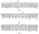
- FIG. 1 to FIG. 8 are respectively described in detail hereinafter.
- the chip packaging structures as illustrated in FIG. 1 and FIG. 2 include a trench penetrating through the substrate 1, where the trench is configured to accommodate the chip 2, and the chip 2 and the substrate 1 are connected by bonding of the wire 4.
- the first electrical connection structure on the substrate 1 may be a pin array, or may be a BGA 5, which is, however, not limited hereto.
- the chip 2 accommodated in the trench of the substrate 1 may be a chip 2 that is processed by the ordinary technique, and a die pad of the chip 2 may be arranged on the surface of the chip 2, and the die pad of the chip 2 is the second electrical connection structure of the chip 2.
- the first electrical connection structure and the second electrical connection structure may be connected by means of an RDL.
- a trench penetrating through the substrate 1 is arranged, the trench is configured to accommodate the chip 2, the plastic package 3 is arranged on the upper surface of the substrate 1, and the chip 2 and the substrate 1 are connected by wire bonding.
- the first electrical connection structure on the substrate 1 may be a pin array (not illustrated in the drawings)
- the chip 2 may be a chip 2 that is processed by the ordinary technique
- the second electrical connection structure of the chip 2 may be a die pad of the chip 2 (not illustrated in the drawings)
- the chip 2 and the substrate 1 are electrically connected by wire bonding.
- the electrical connection between the die pad and the pin array may also be implemented by means of an RDL.
- the first electrical connection structure on the substrate 1 is not limited to the pin array
- the second electrical connection structure of the chip 2 is not limited to the die pad of the chip 2.
- the substrate 1 and the chip 2 are firstly secured to a tooling, and the positions of the substrate 1 and the chip 2 are adjusted according to the design drawing; after the adjustment, a gap is defined between the trench on the substrate 1 and the chip 2, and adhesive is applied into the gap; the bonding layer is formed after the adhesive is cured, where the adhesive may be an underfill adhesive, a UV adhesive, an epoxy adhesive or a thermo-curable adhesive; or an EMC is injected into the gap, and the bonding layer is formed after the EMC is crosslinked and cured; afterwards, the wire 4 such as the metal wire is connected, where one end of the wire 4 is connected to the chip 2, and the other end of the wire 4 is connected to the substrate; and finally, the EMC is injected onto the upper surface of the substrate 1, and the plastic package 3 covering the upper surface of the substrate 1 is
- the plastic package 3 as illustrated in FIG. 1 is arranged on the upper surface of the substrate 1, during assembling of the packaging structure of the chip 2, the lower surface of the chip 2 and the lower surface of the substrate 1 are as much as possible made to be in the same horizontal plane to improve the flatness of the module of the entire chip 2, and further facilitate the subsequent assembling process.
- the chip 2 is accommodated in the trench on the substrate 1 to decrease the thickness of the chip packaging structure and the packaging volume; and the plastic package 3 is configured on the surface of the substrate 1 on which the chip 2 is disposed to plastically package the chip 2, which not only ensures the structural strength of the chip packaging structure, but also reduces the warpage that may be caused due to the decrease of the thickness of the chip packaging structure as much as possible.
- the surface of the plastic package 3 is treated to be a flat surface, such that the chip module has good flatness and the adaptability of the chip module is improved.
- a trench penetrating through the substrate 1 is provided, the trench is configured to accommodate the chip 2, the plastic package 3 is disposed on the upper surface and the lower surface of the substrate 1, and the chip 2 and the substrate 1 are connected by wire bonding.
- the first electrical connection structure on the substrate 1 may be a BGA 5
- the chip 2 may be a chip 2 that is processed by the ordinary technique
- the second electrical connection structure of the chip 2 may be a die pad of the chip 2 (not illustrated in the drawings)
- the chip 2 and the substrate 1 are electrically connected by bonding of the wire 4.
- the electrical connection between the die pad and the pin array may also be implemented by means of an RDL.
- the first electrical connection structure on the substrate 1 is not limited to the BGA 5, and the second electrical connection structure of the chip 2 is not limited to the die pad of the chip 2.
- the substrate 1 and the chip 2 are firstly secured a tooling, and the positions of the substrate 1 and the chip 2 are adjusted according to the design drawing; after the adjustment, a gap is defined between the trench on the substrate 1 and the chip 2, and adhesive is applied into the gap; the bonding layer is formed after the adhesive is cured, where the adhesive may be an underfill adhesive, a UV adhesive, an epoxy adhesive or a thermo-curable adhesive; or an EMC is injected into the gap, and the bonding layer is formed after the EMC is crosslinked and cured; afterwards, the wire 4 such as the metal wire is connected, where one end of the wire 4 is connected to the chip 2, and the other end of the wire 4 is connected to the substrate; and finally, the EMC is injected onto the upper surface and the lower surface of the substrate 1, and the plastic package 3 covering the upper surface and the
- the first electrical connection structure on the substrate 1 in the chip packaging structure as illustrated in FIG. 2 is a BGA 5, which is favorable to ensuring the mechanical reliability of the entire chip module.
- the chip packaging structures as illustrated in FIG. 3 to FIG. 5 include a trench penetrating through the substrate 1, where the trench is configured to accommodate the chip 2, and the chip 2 and the substrate 1 are connected by bonding of the wire 4.
- the first electrical connection structure on the substrate 1 may be a pin array, or may be a BGA 5, which is, however, not limited hereto.
- the chip 2 accommodated in the trench of the substrate 1 may be a chip 2 that is processed by the trenching technique, a trench 21 may be formed after the chip 2 is subjected to trenching, where the trench 21 may be provided with a die pad of the chip 2, and the die pad of the chip 2 is the second electrical connection structure of the chip 2.
- the first electrical connection structure and the second electrical connection structure may be connected by means of an RDL.
- a trench 21 is arranged on the chip 2, and the first electrical connection structure of the chip 2 is arranged in the trench 21.
- the thickness and volume of the packaging structure of the chip 2 may be further reduced.
- a trench penetrating through the substrate 1 is arranged, the trench is configured to accommodate the chip 2, the plastic package 3 is arranged on the upper surface of the substrate 1, and the chip 2 and the substrate 1 are connected by wire bonding.
- the first electrical connection structure on the substrate 1 may be a pin array (not illustrated in the drawings)
- the chip 2 may be a chip 2 that is processed by the trenching technique
- the second electrical connection structure of the chip 2 may be a die pad of the chip 2 (not illustrated in the drawings) and arranged in the trench 21 of the chip 2
- the chip 2 and the substrate 1 are electrically connected by bonding of the wire 4.
- the electrical connection between the die pad and the pin array may also be implemented by means of an RDL.
- the first electrical connection structure on the substrate 1 is not limited to the pin array
- the second electrical connection structure of the chip 2 is not limited to the die pad of the chip 2.
- the substrate 1 and the chip 2 are firstly secured to a tooling, and the positions of the substrate 1 and the chip 2 are adjusted according to the design drawing; after the adjustment, a gap is defined between the trench on the substrate 1 and the chip 2, and adhesive is applied into the gap; the bonding layer is formed after the adhesive is cured, where the adhesive may be an underfill adhesive, a UV adhesive, an epoxy adhesive or a thermo-curable adhesive; or an EMC is injected into the gap, and the bonding layer is formed after the EMC is crosslinked and cured; afterwards, the wire 4 such as the metal wire is connected, where one end of the wire 4 is connected to the chip 2, and the other end of the wire 4 is connected to the substrate; and finally, the EMC is injected onto the upper surface of the substrate 1, and the plastic package 3 covering the upper surface of the substrate 1 is formed after the EMC is crosslinked and cured.
- the plastic package 3 as illustrated in FIG. 1 is arranged on the upper surface of the substrate 1, during assembling of the packaging structure of the chip 2, the lower surface of the chip 2 and the lower surface of the substrate 3 are as much as possible made to be in the same horizontal plane to improve the flatness of the entire chip module, and further facilitate the subsequent assembling process.
- the chip 2 is processed by the TSV technique to accommodate the second electrical connection structure of the chip 2 in the trench 21 and accommodate the chip 2 in the trench of the substrate 1, such that the thickness of the chip packaging structure and the packaging volume are reduced; and the plastic package 3 is provided on the upper surface of the substrate 1 on which the chip 2 is accommodated to plastically package the chip 2, which not only ensures the structural strength of the chip packaging structure, but also reduces the warpage that may be caused due to the decrease of the thickness of the chip packaging structure as much as possible.
- the surface of the plastic package 3 is treated to be a flat surface, such that the chip module has good flatness and the adaptability of the chip module is improved.
- a trench penetrating through the substrate 1 is arranged, the trench is configured to accommodate the chip 2, the plastic package 3 is arranged on the lower surface of the substrate 1, and the chip 2 and the substrate 1 are connected by wire bonding.
- the first electrical connection structure on the substrate 1 may be a BGA 5
- the chip 2 may be a chip 2 that is processed by the trenching technique
- the second electrical connection structure of the chip 2 may be a die pad (not illustrated in the drawings) and arranged in the trench 21 of the chip 2
- the chip 2 and the substrate 1 are electrically connected by bonding of the wire 4.
- the electrical connection between the die pad of the chip 2 and the BGA 5 may also be implemented by means of an RDL.
- the first electrical connection structure on the substrate 1 is not limited to the BGA 5, and the second electrical connection structure of the chip 2 is not limited to the die pad of the chip 2.
- the substrate 1 and the chip 2 are firstly secured to a tooling, and the positions of the substrate 1 and the chip 2 are adjusted according to the design drawing; after the adjustment, a gap is defined between the trench on the substrate 1 and the chip 2, and adhesive is applied into the gap; the bonding layer is formed after the adhesive is cured, where the adhesive may be an underfill adhesive, a UV adhesive, an epoxy adhesive or a thermo-curable adhesive; or an EMC is injected into the gap, and the bonding layer is formed after the EMC is crosslinked and cured; afterwards, the wire 4 such as the metal wire is connected, where one end of the wire 4 is connected to the chip 2, and the other end of the wire 4 is connected to the substrate; and finally, the EMC is injected onto the lower surface of the substrate 1, and the plastic package 3 covering the lower surface of the substrate 1 is
- a layer of the plastic package 3 having a small thickness is arranged on the upper surface of the substrate 1 to fill the trench 21.
- the chip 2 is processed by the TSV technique to accommodate the second electrical connection structure of the chip 2 in the trench 21 and accommodate the chip 2 in the trench of the substrate 1, such that the thickness of the chip packaging structure and the packaging volume are reduced; and the plastic package 3 is configured on the lower surface of the substrate 1 on which the chip 2 is disposed to plastically package the chip 2, which not only ensures the structural strength of the chip packaging structure, but also reduces the warpage that may be caused due to the decrease of the thickness of the chip packaging structure as much as possible.
- the surface of the plastic package 3 is treated to be a flat surface, such that the chip module has good flatness and the adaptability of the chip module is improved.
- the first electrical connection structure on the substrate 1 is a BGA 5, which is favorable to ensuring the mechanical reliability of the entire chip module.
- a trench penetrating through the substrate 1 is arranged, the trench is configured to accommodate the chip 2, the plastic package 3 is arranged on the upper surface and the lower surface of the substrate 1, and the chip 2 and the substrate 1 are connected by wire bonding.
- the first electrical connection structure on the substrate 1 may be a BGA 5
- the chip 2 may be a chip 2 that is processed by the trenching technique
- the second electrical connection structure of the chip 2 may be a die pad of the chip 2 (not illustrated in the drawings) and arranged in the trench 21 of the chip 2
- the chip 2 and the substrate 1 are electrically connected by wire bonding.
- the electrical connection between the die pad of the chip 2 and the BGA 5 may also be implemented by means of an RDL.
- the first electrical connection structure on the substrate 1 is not limited to the BGA 5
- the second electrical connection structure of the chip 2 is not limited to the die pad of the chip 2.
- the substrate 1 and the chip 2 are firstly secured to a tooling, and the positions of the substrate 1 and the chip 2 are adjusted according to the design drawing; after the adjustment, a gap is defined between the trench on the substrate 1 and the chip 2, and adhesive is applied into the gap; the bonding layer is formed after the adhesive is cured, where the adhesive may be an underfill adhesive, a UV adhesive, an epoxy adhesive or a thermo-curable adhesive; and an EMC is injected into the gap, and the bonding layer is formed after the EMC is crosslinked and cured; afterwards, the wire 4 such as the metal wire is connected, where one end of the wire 4 is connected to the chip 2, and the other end of the wire 4 is connected to the substrate; and finally, the EMC is injected onto the upper surface and the lower surface of the substrate 1, and the plastic package 3 covering the upper surface and the lower surface of the substrate 1 is formed after the EMC is crosslinked and cured.
- the first electrical connection structure on the substrate 1 in the chip packaging structure as illustrated in FIG. 5 is a BGA 5, which is favorable to ensuring the mechanical reliability of the entire chip module.
- the chip packaging structures as illustrated in FIG. 6 to FIG. 8 includes a trench penetrating through the substrate 1, where the trench is configured to accommodate the chip 2.
- the first electrical connection structure on the substrate 1 is a pin array or a BGA 5, which is, however, not limited hereto; and the chip 2 is a chip 2 that is processed by the TSV technique, and a TSV structure (not illustrated in the drawings) penetrates through the chip 2, where the TSV structure is the second electrical connection structure of the chip 2.
- the first electrical connection structure and the second electrical connection structure may be connected by means of an RDL.
- the chip 2 that is processed by the TSV technique is used, and it is unnecessary to arranged a die pad on the chip 2 and configure the wire 4 for wire bonding, such that the mounting space is saved, and the thickness of the chip packaging structure and the thickness of the module of the chip 2 are further reduced.
- the chip packaging structure as illustrated in FIG. 6 a trench penetrating through the substrate 1 is arranged, the trench is configured to accommodate the chip 2, the plastic package 3 is arranged on the upper surface and the lower surface of the substrate 1.
- the first electrical connection structure on the substrate 1 is a pin array (not illustrated in the drawings)
- the chip 2 is a chip 2 that is processed by the TSV technique
- a TSV structure (not illustrated in the drawings) penetrates through the chip 2, where the TSV structure is the second electrical connection structure of the chip 2.
- the electrical connection the TSV structure and the pin array may be implemented by means of an RDL. Nevertheless, the first electrical connection structure on the substrate 1 is not limited to the pin array.
- the substrate 1 and the chip 2 are firstly secured to a tooling, and the positions of the substrate 1 and the chip 2 are adjusted based on the design drawing; after the adjustment, a gap is defined between the trench on the substrate 1 and the chip 2, and adhesive is applied to into the gap; the bonding layer is formed after the adhesive is cured, where the adhesive may be an underfill adhesive, a UV adhesive, an epoxy adhesive or a thermo-curable adhesive; or an EMC is injected into the gap; and afterwards, the EMC is injected onto the upper surface of the substrate 1, and the plastic package 3 covering the upper surface of the substrate 1 is formed after the EMC is crosslinked and cured. It should be noted that since the plastic package 6 as illustrated in FIG.
- the lower surface of the chip 2 and the lower surface of the substrate 3 are as much as possible made to be in the same horizontal plane to improve the flatness of the entire chip module, and further facilitate the subsequent assembling process.
- the chip 2 that is processed by the TSV technique is provided, and the chip 2 is accommodated in the trench of the substrate 1 to decrease the thickness of the chip packaging structure and the packaging volume; and the plastic package 3 is configured on the upper surface of the substrate 1 on which the chip 2 is disposed to plastically package the chip 2, which not only ensures the structural strength of the chip packaging structure, but also reduces the warpage that may be caused due to the decrease of the thickness of the chip packaging structure as much as possible.
- the surface of the plastic package 3 is treated to be a flat surface, such that the chip module has good flatness and the adaptability of the chip module is improved.
- the chip packaging structure as illustrated in FIG. 7 a trench penetrating through the substrate 1 is arranged, the trench is configured to accommodate the chip 2, the plastic package 3 is arranged on the lower surface and the lower surface of the substrate 1.
- the first electrical connection structure on the substrate 1 is a BGA 5
- the chip 2 is a chip 2 that is processed by the TSV technique
- a TSV structure (not illustrated in the drawings) penetrates through the chip 2, where the TSV structure is the second electrical connection structure of the chip 2.
- the electrical connection the TSV structure and the pin array may be implemented by means of an RDL.
- the first electrical connection structure on the substrate 1 is not limited to the BGA 5.
- a tin ball pad is additionally arranged below the chip 2 that is processed by the TSV technique according to practical needs, where the pad is provided with a plurality of tin balls, the pad is electrically connected to the TSV structure via the tin balls on the tin ball pad, and the electrical connection between the tin ball pad and the BGA 5 on the substrate is implemented by means of an RDL.
- the substrate 1 and the chip 2 are firstly secured to a tooling, and the positions of the substrate 1 and the chip 2 are adjusted based on the design drawing; after the adjustment, a gap is defined between the trench on the substrate 1 and the chip 2, and adhesive is applied to into the gap; the bonding layer is formed after the adhesive is cured, where the adhesive may be an underfill adhesive, a UV adhesive, an epoxy adhesive or a thermo-curable adhesive; or an EMC is injected into the gap; and afterwards, the EMC is injected onto the lower surface of the substrate 1, and the plastic package 3 covering the lower surface of the substrate 1 is formed after the EMC is crosslinked and cured. It should be noted that since the plastic package 7 as illustrated in FIG.
- the upper surface of the chip 2 and the upper surface of the substrate 3 are as much as possible made to be in the same horizontal plane to improve the flatness of the entire chip module, and further facilitate the subsequent assembling process.
- the chip 2 that is processed by the TSV technique is provided, and the chip 2 is accommodated in the trench on the substrate 1 to decrease the thickness of the chip packaging structure and the packaging volume; and the plastic package 3 is disposed on the lower surface of the substrate 1 on which the chip 2 is disposed to plastically package the chip 2, which not only ensures the structural strength of the chip packaging structure, but also reduces the warpage that may be caused due to the decrease of the thickness of the chip packaging structure as much as possible.
- the surface of the plastic package 3 is treated to be a flat surface, such that the chip module has good flatness and the adaptability of the chip module is improved.
- the first electrical connection structure on the substrate 1 is a BGA 5, which is favorable to ensuring the mechanical reliability of the entire chip module.
- the chip packaging structure as illustrated in FIG. 8 a trench penetrating through the substrate 1 is arranged, the trench is configured to accommodate the chip 2, the plastic package 3 is arranged on the upper surface of the substrate 1.
- the first electrical connection structure on the substrate 1 is a BGA 5
- the chip 2 is a chip 2 that is processed by the TSV technique
- a TSV structure (not illustrated in the drawings) penetrates through the chip 2, where the TSV structure is the second electrical connection structure of the chip 2.
- the electrical connection the TSV structure and the pin array may be implemented by means of an RDL.
- the first electrical connection structure on the substrate 1 is not limited to the BGA 5.
- the substrate 1 and the chip 2 are firstly secured to a tooling, and the positions of the substrate 1 and the chip 2 are adjusted based on the design drawing; after the adjustment, a gap is defined between the trench on the substrate 1 and the chip 2, and adhesive is applied to into the gap; the bonding layer is formed after the adhesive is cured, where the adhesive may be an underfill adhesive, a UV adhesive, an epoxy adhesive or a thermo-curable adhesive; or an EMC is injected into the gap; afterwards, the EMC is injected onto the upper surface and the lower surface of the substrate 1, and the plastic package 3 covering the upper surface and the lower surface of the substrate 1 is formed after the EMC is crosslinked and cured.
- the adhesive may be an underfill adhesive, a UV adhesive, an epoxy adhesive or a thermo-curable adhesive
- the chip packaging structure as illustrated in FIG. 8 by using the plastic package 3 that covers the upper surface and the lower surface of the substrate 1, the chip 2 and the substrate 1 are better protected, such that the chip module packaged by using the chip packaging structure has good contamination resistance and scratch resistance and the like.
- the number of pads, for example, BGAs 5 arranged below the substrate may be determined according to practical needs of the chip, and the number of pads in the drawings for the specification is only an exemplary value, which is not particularly limited.
- the chip module includes: a chip and the chip packaging structure according to any one of the above embodiments of the present application; where the chip is accommodated in the trench on the substrate of the chip packaging structure. It should be noted that the structure, the functionality and the technical effect of the chip packaging structure are similar to those disclosed in the above embodiments, which are thus not described herein any further.
- the substrate is accommodated in the trench on the substrate to decrease the thickness of the chip packaging structure and the volume of the package; and the plastic package is configured on the surface of the substrate on which the chip is disposed to plastically package the chip, which not only ensures the structural strength of the chip packaging structure, but also reduces the warpage that may be caused due to the decrease of the thickness of the chip packaging structure as much as possible.
- the surface of the plastic package is treated to be a flat surface, such that the chip module has good flatness and the adaptability of the chip module is improved.
- An embodiment of the present application further provides an electronic terminal.
- the electronic terminal includes the chip module as described in any one of the above embodiments. It should be noted that the structure, the functionality and the technical effect of the chip module are similar to those disclosed in the above embodiments, which are thus not described herein any further.
- the chip module of the electronic terminal includes a chip packaging structure.
- the chip is accommodated in the trench of the substrate to decrease the thickness and volume of the chip packaging structure; and the plastic package is provided on the surface of the substrate on which the chip is disposed to plastically package the chip, which not only ensures the structural strength of the chip packaging structure, but also reduces the warpage that may be caused due to the decrease of the thickness of the chip packaging structure as much as possible.
- the surface of the plastic package is treated to be a flat surface, such that the chip module has good flatness and the adaptability of the chip module is improved.
Landscapes
- Structures Or Materials For Encapsulating Or Coating Semiconductor Devices Or Solid State Devices (AREA)
- Engineering & Computer Science (AREA)
- Microelectronics & Electronic Packaging (AREA)
- Encapsulation Of And Coatings For Semiconductor Or Solid State Devices (AREA)
Abstract
Description
- The present application relates to the technical field of chip packaging, and in particular, relates to a chip packaging structure, a chip module and an electronic terminal.
- With the constant development of mobile terminals into small size and ultra-small thickness, functional modules applied to the mobile terminals are also developing to be small-sized and thinner. For example, most mobile terminals are equipped with a chip packaging structure. By the chip packaging structure, the identity of a user is verified to start the mobile terminal.
- However, the chip packaging structure having small size and thickness is easily subjected to warpage. Therefore, how to reduce the warpage of the chip packaging structure is a technical problem to be urgently solved.
- Embodiments of the present application are intended to provide a chip packaging structure, a chip module and an electronic terminal, to solve the above technical problems in the prior art.
- A first aspect of embodiments of the present application provides a chip packaging structure. The chip packaging structure includes a substrate and a plastic package.
- The substrate is provided with a trench, where the trench is configured to accommodate a chip.
- The plastic package is configured to cover an upper surface of the substrate on which the chip is disposed, and an upper surface of the plastic package is a flat surface; and/or the plastic package is configured to cover a lower surface of the substrate on which the chip is disposed, and a lower surface of the plastic package is a flat surface.
- Optionally, an upper surface of the chip and the upper surface of the substrate are in the same horizontal plane; and/or
a lower surface of the chip and the lower surface of the substrate are in the same horizontal plane. - Optionally, the substrate is further provided with a first electrical connection structure connected to a peripheral circuit, where the first electrical connection structure is configured to be electrically connected to a second electrical connection structure arranged on the chip.
- Optionally, the first electrical connection structure is electrically connected to the second electrical connection structure on the chip that is disposed at a bottom of the trench.
- Optionally, the first electrical connection structure is connected to the second electrical connection structure by wire bonding.
- Optionally, the first electrical connection structure is electrically connected to a through silicon via arranged on the chip.
- Optionally, the first electrical connection structure is a ball grid array.
- Optionally, the plastic package is formed by an injected epoxy resin via a crosslinking curing reaction.
- Optionally, the substrate is bonded to the accommodated chip via a bonding layer.
- Optionally, the bonding layer is formed by an injected epoxy molding compound (EMC) via a crosslinking curing reaction.
- Optionally, the substrate has a thickness of between 0.08 mm and 5 mm.
- A second aspect of embodiments of the present application provides a chip module. The chip module includes: a chip and the chip packaging structure according to the first aspect of embodiments of the present application; where the chip is accommodated in the trench on the substrate of the chip packaging structure.
- A third aspect of embodiments of the present application provides an electronic terminal. The electronic terminal includes the chip module according to the second aspect of embodiments of the present application.
- Embodiments of the present application provide the chip packaging structure, the chip module and the electronic terminal. In the chip packaging structure, the chip is accommodated in the trench on the substrate to decrease the thickness of the chip packaging structure and the packaging volume; and the plastic package is configured on the surface of the substrate on which the chip is disposed to plastically package the chip, which not only ensures the structural strength of the chip packaging structure, but also reduces the warpage that may be caused due to the decrease of the thickness of the chip packaging structure as much as possible. In addition, the surface of the plastic package is treated to be a flat surface, such that the chip module has good flatness and the adaptability of the chip module is improved.
- To more clearly describe technical solutions according to the embodiments of the present application or in the prior art, drawings that are to be referred for description of the embodiments or the prior art are briefly described hereinafter. Apparently, the drawings described hereinafter merely illustrate some embodiments of the present application. Persons of ordinary skill in the art may also derive other drawings based on the drawings described herein without any creative effort.
-
FIG. 1 is a schematic structural view of a chip packaging structure according to the first embodiment of the present application; -
FIG. 2 is a schematic structural view of a chip packaging structure according to the second embodiment of the present application; -
FIG. 3 is a schematic structural view of a chip packaging structure according to the third embodiment of the present application; -
FIG. 4 is a schematic structural view of a chip packaging structure according to the fourth embodiment of the present application; -
FIG. 5 is a schematic structural view of a chip packaging structure according to the fifth embodiment of the present application; -
FIG. 6 is a schematic structural view of a chip packaging structure according to the sixth embodiment of the present application; -
FIG. 7 is a schematic structural view of a chip packaging structure according to the seventh embodiment of the present application; and -
FIG. 8 is a schematic structural view of a chip packaging structure according to the eighth embodiment of the present application. - To make the objectives, technical features, and advantages of the present application clearer and more understandable, the technical solutions according to the embodiments of the present application are further described in detail with reference to the accompany drawings. Apparently, the embodiments described herein are merely some exemplary ones, rather than all the embodiments of the present application. Based on the embodiments of the present application, all other embodiments derived by persons of ordinary skill in the art without any creative efforts shall fall within the protection scope of the present application.
- Referring to
FIG. 1 to FIG. 8 , a chip packaging structure according to this embodiment includes: asubstrate 1 and aplastic package 3; where thesubstrate 1 is provided with a trench, the trench being configured to accommodate achip 2; theplastic package 3 is configured to cover an upper surface of thesubstrate 1 on which thechip 2 is disposed. An upper surface of theplastic package 3 is a flat surface; and/or theplastic package 3 is configured to cover a lower surface of thesubstrate 1 on which thechip 2 is disposed, and a lower surface of theplastic package 3 is a flat surface. - In the chip packaging structure according to this embodiment, the
chip 2 is accommodated in the trench of thesubstrate 1 to decrease the thickness and volume of the chip packaging structure; and theplastic package 3 is provided on the surface of thesubstrate 1 on which thechip 2 is disposed to plastically package thechip 2, which not only ensures the structural strength of the chip packaging structure, but also reduces the warpage that may be caused due to the decrease of the thickness of the chip packaging structure as much as possible. In addition, the surface of theplastic package 3 is treated to be a flat surface, such that the chip module has good flatness and the adaptability of the chip module is improved. - Specifically, the chip packaging structure is capable of achieving a securing, protection and the like effects on the
chip 2. Securing of thechip 2 is in one aspect dependent on securing of thesubstrate 1, and in another aspect dependent on securing of theplastic package 3. For assurance of the structural strength of the chip packaging structure, it is required that thesubstrate 1 needs to have good hardness in addition to good processing properties. Optionally, thesubstrate 1 may be made of acryl, iron, copper or glass fiber. Thesubstrate 1 made of these materials has good hardness. - Specifically, according to this embodiment, the
chip 2 is disposed in the trench on thesubstrate 1, to decrease the thickness and volume of the chip packaging structure. It should be noted that the position of the trench and the structural form of the trench are not specifically limited, and may be determined according to the specific structure of thechip 2. Preferably, the trench is in the central region of thesubstrate 1, and the trench is a through trench which penetrates through thesubstrate 1. In this way, thechip 2 may be maximally disposed in thesubstrate 1, and the thickness and volume of the chip packaging structure may be reduced as much as possible. However, in practical application, the trench may be defined as partially penetrating through thesubstrate 1 and partially not penetrating through thesubstrate 1, or defined as a non-penetration structure according to practical needs, which is not limited in the embodiments of the present application. Optionally, after thechip 2 is accommodated, the upper surface of thechip 2 and the upper surface of thesubstrate 1 may be in the same horizontal plane; and/or the lower surface of thechip 2 and the lower surface of thesubstrate 1 may be in the same horizontal plane. For example, the thickness of thechip 2 may be greater than, equal to, or less than the thickness of thesubstrate 1. When thechip 2 is assembled in the trench of thesubstrate 1, a surface of thechip 2 and a surface of thesubstrate 1 are made to be in the same horizontal plane as much as possible. As such, when thechip 2 is assembled on thesubstrate 1, whether the assembling of thechip 2 on thesubstrate 1 satisfies a design requirement is determined by determining whether the surfaces of thechip 2 and thesubstrate 1 are in the same horizontal plane. This, to some extent, facilitates rapid assembling of thechip 2 on thesubstrate 1 and also subsequent processing and manufacturing of the chip packaging structure. Still for example, in this embodiment, in terms of satisfying the defined requirement of the structural strength, the thickness of thesubstrate 1 may be selected from the range of 0.08 mm to 0.5 mm. When the chip is disposed in the substrate, the thickness of the chip module may be controlled to be about 0.24 mm, and the warpage of the chip module may be controlled to be in the range of 5 to 80 µm. When the chip module is applied to an identification module for identifying a biological feature, the thickness of the biological feature identification module may be controlled to be about 0.45 mm. In this way, the chip module satisfies the requirements of both small thickness and low-warpage. - It should be noted that a connection manner between the
substrate 1 and thechip 2 is not specifically limited. Optionally, thesubstrate 1 is bonded to the accommodatedchip 2 via a bonding layer. For example, during assembling, thesubstrate 1 and thechip 2 are firstly secured to a tooling, and the positions of thesubstrate 1 and thechip 2 are adjusted based on a design drawing of the chip packaging structure; after the adjustment, a gap is defined between the trench of thesubstrate 1 and thechip 2, and adhesive is applied into the gap; the bonding layer is formed after the adhesive is cured. The adhesive may be an underfill adhesive, a UV adhesive, an epoxy adhesive or a thermo-curable adhesive. Or an epoxy molding compound (EMC) can be injected into the gap, and the bonding layer is formed after the EMC is crosslinked and cured. According to this embodiment, by bonding thesubstrate 1 to the accommodatedchip 2, thechip 1 is better secured. In addition, since the surroundings of thechip 2 are all bonded, the structural strength of the chip packaging structure is improved to some extent. - Apparently, by arranging the
plastic package 3 on the chip packaging structure, thechip 2 and thesubstrate 1 are well protected, and the structural strength of the chip packaging structure with thechip 2 being accommodated in the trench is enhanced. For example, after thechip 2 is disposed in the trench on thesubstrate 1, the EMC is injected onto the upper surface of thesubstrate 1, and the EMC forms, through crosslinking and curing, theplastic package 3 that covers the upper surface of thesubstrate 1. Nevertheless, the EMC may also be injected onto the lower surface of thesubstrate 1, and the EMC forms, through crosslinking and curing, theplastic package 3 that covers the lower surface of thesubstrate 1. In addition, the EMC may also be injected onto both the upper surface and the lower surface of thesubstrate 1, and the EMC forms, through crosslinking and curing, theplastic package 3 that covers the upper surface and the lower surface of thesubstrate 1. It should be noted that the plastic package is not limited to the plastic package formed by the EMC through crosslinking and curing that is exemplified as above, and may be made of any suitable material having the plastic packaging function. Further, to improve the flatness of the chip packaging structure, in arranging theplastic package 3, the surface of theplastic package 3 should be made to form a flat surface. Specifically, theplastic package 3 is configured to cover the upper surface of thesubstrate 1 on which thechip 2 is accommodated, and the upper surface of theplastic package 3 is a flat surface; and/or theplastic package 3 is configured to cover the lower surface of thesubstrate 1 on which thechip 2 is accommodated, and the lower surface of theplastic package 3 is a flat surface. - Optionally, the
substrate 1 is further provided with a first electrical connection structure connected to a peripheral circuit, where the first electrical connection structure is configured to be electrically connected to a second electrical connection structure arranged on thechip 2. - For example, the first electrical connection structure arranged on the
substrate 1 may be a pin array that is connected to the peripheral circuit or aball grid array 5 arranged on thesubstrate 1, which is not limited hereto. Using theball grid array 5 as an example, as compared with the pin form, the ball grid array (BGA) 5 is favorable to ensuring the mechanical reliability of the entire chip module. For example, theball grid array 5 is a pad arranged below thesubstrate 1. - Specifically, the chip according to this embodiment may be a chip processed by an ordinary technique, or may be a chip processed by a trenching technique, or may be a chip processed by a through silicon vias (TSV) technique, which is not limited hereto.
- For example, when the
chip 2 is a chip processed by the ordinary technique, the second electrical connection structure may be arranged on the upper surface and/or the lower surface of thechip 2, and the second electrical connection structure may be a die pad. In this case, the first electrical connection structure and the second electrical connection structure may be connected to each other via wire bonding. The specific implementation manner of the wire bonding may be referenced to the conventional implementation manner, which is not described herein any further. The wire bonding implements electrical interconnection between the chip and the substrate by using a thin metal line. Optionally, the metal line may be any one of a gold line, an aluminum line and a copper line, which is, however, not limited hereto. - For example, when the
chip 2 is processed by the trenching technique, atrench 21 is formed on thechip 2, the second electrical connection structure may be arranged in thetrench 21, and the second electrical connection structure may be a die pad. In this case, the first electrical connection structure and the second electrical connection structure may be connected to each other via bonding of awire 4. The specific implementation manner of the wire bonding may be referenced to the conventional implementation manner, which is not described herein any further. According to this embodiment, by trenching of the chip, the thickness of the chip packaging structure may be further reduced; and after the trenching, the thickness of the chip packaging structure may not be increased even the wire bonding is employed. - It should be noted that the
trench 21 may be formed at the upper part of thechip 2, or may be formed at the lower part of thechip 2, and one or a plurality oftrenches 21 may be arranged. Further, when thetrench 21 is formed at the upper part of thechip 2, the distance from the bottom surface of thetrench 21 to the upper surface of the chip is defined as a predetermined distance; and when the trench is formed at the lower part of thechip 2, the distance from the bottom surface of thetrench 21 to the lower surface of thechip 2 is defined as a predetermined distance. The predetermined distance is defined to maximally reduce the thickness of the chip packaging structure, which meanwhile may ensure that the stress suffered by the wire in the wire bonding causes no damage to the structure of the wire and thus the electrical performance of the chip module may not be affected. The predetermined difference threshold may be appropriately defined by a person skilled in the art according to practical needs, which is not limited in the embodiment of the present application. - For example, when the
chip 2 is processed by the TSV technique, the through silicon via structure penetrates through thechip 2, and copper, tungsten, polycrystalline silicon or the like electrically conductive substance may be filled in the through silicon via. The through silicon via structure is the second electrical connection structure that is electrically connected to the first electrical connection structure on thesubstrate 1. Thechip 2 processed by the TSV technique is capable of further reducing the thickness of the package structure of thechip 2 and the thickness of the module of thechip 2. - It should be noted that the first electrical connection structure and the second electrical connection structure may be directly electrically connected, or may be indirectly electrically connected. The direct electrical connection refers to that the first electrical connection structure and the second electrical connection structure are in direct contact with each other and thus electrically connected to each other, and the indirect electrical connection refers to that the first electrical connection structure and the second electrical connection structure are electrically connected to each other via an intermediate electrically conductive structure. For example, when the first electrical connection structure is the
ball grid array 5 arranged below thesubstrate 1, the second electrical connection structure may be a die pad. In this case, the first electrical connection structure and the second electrical connection structure are distal from each other in terms of space, and may not be electrically connected to each other. In this case, a redistribution layer (RDL) may be arranged on thesubstrate 1 to implement the first electrical connection structure and the second electrical connection structure. Likewise, when the first electrical connection structure is theball grid array 5 arranged below thesubstrate 1, the second electrical connection structure may be a through silicon via structure. In this case, the first electrical connection structure and the second electrical connection structure are distal from each other in terms of space, and may not be electrically connected to each other. In this case, an RDL may be arranged on thesubstrate 1 to implement the first electrical connection structure and the second electrical connection structure. The specific manner of arranging the RDL may be referenced to the conventional implementation manner, which is not described herein any further. - The chip packaging structures as illustrated in
FIG. 1 to FIG. 8 are respectively described in detail hereinafter. - The chip packaging structures as illustrated in
FIG. 1 and FIG. 2 include a trench penetrating through thesubstrate 1, where the trench is configured to accommodate thechip 2, and thechip 2 and thesubstrate 1 are connected by bonding of thewire 4. The first electrical connection structure on thesubstrate 1 may be a pin array, or may be aBGA 5, which is, however, not limited hereto. Thechip 2 accommodated in the trench of thesubstrate 1 may be achip 2 that is processed by the ordinary technique, and a die pad of thechip 2 may be arranged on the surface of thechip 2, and the die pad of thechip 2 is the second electrical connection structure of thechip 2. The first electrical connection structure and the second electrical connection structure may be connected by means of an RDL. - Specifically, in the chip packaging structure as illustrated in
FIG. 1 , a trench penetrating through thesubstrate 1 is arranged, the trench is configured to accommodate thechip 2, theplastic package 3 is arranged on the upper surface of thesubstrate 1, and thechip 2 and thesubstrate 1 are connected by wire bonding. The first electrical connection structure on thesubstrate 1 may be a pin array (not illustrated in the drawings), thechip 2 may be achip 2 that is processed by the ordinary technique, the second electrical connection structure of thechip 2 may be a die pad of the chip 2 (not illustrated in the drawings), and thechip 2 and thesubstrate 1 are electrically connected by wire bonding. According to practical needs, the electrical connection between the die pad and the pin array may also be implemented by means of an RDL. Nevertheless, the first electrical connection structure on thesubstrate 1 is not limited to the pin array, and the second electrical connection structure of thechip 2 is not limited to the die pad of thechip 2. During assembling of the chip packaging structure, thesubstrate 1 and thechip 2 are firstly secured to a tooling, and the positions of thesubstrate 1 and thechip 2 are adjusted according to the design drawing; after the adjustment, a gap is defined between the trench on thesubstrate 1 and thechip 2, and adhesive is applied into the gap; the bonding layer is formed after the adhesive is cured, where the adhesive may be an underfill adhesive, a UV adhesive, an epoxy adhesive or a thermo-curable adhesive; or an EMC is injected into the gap, and the bonding layer is formed after the EMC is crosslinked and cured; afterwards, thewire 4 such as the metal wire is connected, where one end of thewire 4 is connected to thechip 2, and the other end of thewire 4 is connected to the substrate; and finally, the EMC is injected onto the upper surface of thesubstrate 1, and theplastic package 3 covering the upper surface of thesubstrate 1 is formed after the EMC is crosslinked and cured. It should be noted that since theplastic package 3 as illustrated inFIG. 1 is arranged on the upper surface of thesubstrate 1, during assembling of the packaging structure of thechip 2, the lower surface of thechip 2 and the lower surface of thesubstrate 1 are as much as possible made to be in the same horizontal plane to improve the flatness of the module of theentire chip 2, and further facilitate the subsequent assembling process. In the chip packaging structure according to this embodiment, thechip 2 is accommodated in the trench on thesubstrate 1 to decrease the thickness of the chip packaging structure and the packaging volume; and theplastic package 3 is configured on the surface of thesubstrate 1 on which thechip 2 is disposed to plastically package thechip 2, which not only ensures the structural strength of the chip packaging structure, but also reduces the warpage that may be caused due to the decrease of the thickness of the chip packaging structure as much as possible. In addition, the surface of theplastic package 3 is treated to be a flat surface, such that the chip module has good flatness and the adaptability of the chip module is improved. - Specifically, in the chip packaging structure as illustrated in
FIG. 2 , a trench penetrating through thesubstrate 1 is provided, the trench is configured to accommodate thechip 2, theplastic package 3 is disposed on the upper surface and the lower surface of thesubstrate 1, and thechip 2 and thesubstrate 1 are connected by wire bonding. The first electrical connection structure on thesubstrate 1 may be aBGA 5, thechip 2 may be achip 2 that is processed by the ordinary technique, the second electrical connection structure of thechip 2 may be a die pad of the chip 2 (not illustrated in the drawings), and thechip 2 and thesubstrate 1 are electrically connected by bonding of thewire 4. According to practical needs, the electrical connection between the die pad and the pin array may also be implemented by means of an RDL. Nevertheless, the first electrical connection structure on thesubstrate 1 is not limited to theBGA 5, and the second electrical connection structure of thechip 2 is not limited to the die pad of thechip 2. During assembling of the chip packaging structure, thesubstrate 1 and thechip 2 are firstly secured a tooling, and the positions of thesubstrate 1 and thechip 2 are adjusted according to the design drawing; after the adjustment, a gap is defined between the trench on thesubstrate 1 and thechip 2, and adhesive is applied into the gap; the bonding layer is formed after the adhesive is cured, where the adhesive may be an underfill adhesive, a UV adhesive, an epoxy adhesive or a thermo-curable adhesive; or an EMC is injected into the gap, and the bonding layer is formed after the EMC is crosslinked and cured; afterwards, thewire 4 such as the metal wire is connected, where one end of thewire 4 is connected to thechip 2, and the other end of thewire 4 is connected to the substrate; and finally, the EMC is injected onto the upper surface and the lower surface of thesubstrate 1, and theplastic package 3 covering the upper surface and the lower surface of thesubstrate 1 is formed after the EMC is crosslinked and cured. Based on the chip packaging structure as illustrated inFIG. 1 , in the chip packaging structure as illustrated inFIG. 2 , by means of theplastic package 3 that covers the upper surface and the lower surface of thesubstrate 1, thechip 2 and thesubstrate 1 are better protected, such that the chip module packaged by using the chip packaging structure has good contamination resistance and scratch resistance and the like. The first electrical connection structure on thesubstrate 1 in the chip packaging structure as illustrated inFIG. 2 is aBGA 5, which is favorable to ensuring the mechanical reliability of the entire chip module. - The chip packaging structures as illustrated in
FIG. 3 to FIG. 5 include a trench penetrating through thesubstrate 1, where the trench is configured to accommodate thechip 2, and thechip 2 and thesubstrate 1 are connected by bonding of thewire 4. The first electrical connection structure on thesubstrate 1 may be a pin array, or may be aBGA 5, which is, however, not limited hereto. Thechip 2 accommodated in the trench of thesubstrate 1 may be achip 2 that is processed by the trenching technique, atrench 21 may be formed after thechip 2 is subjected to trenching, where thetrench 21 may be provided with a die pad of thechip 2, and the die pad of thechip 2 is the second electrical connection structure of thechip 2. The first electrical connection structure and the second electrical connection structure may be connected by means of an RDL. In the chip packaging structures as illustrated inFIG. 3 to FIG. 5 , atrench 21 is arranged on thechip 2, and the first electrical connection structure of thechip 2 is arranged in thetrench 21. As compared with the chip packaging structures as illustrated inFIG. 1 and FIG. 2 , the thickness and volume of the packaging structure of thechip 2 may be further reduced. - Specifically, in the chip packaging structure as illustrated in
FIG. 3 , a trench penetrating through thesubstrate 1 is arranged, the trench is configured to accommodate thechip 2, theplastic package 3 is arranged on the upper surface of thesubstrate 1, and thechip 2 and thesubstrate 1 are connected by wire bonding. The first electrical connection structure on thesubstrate 1 may be a pin array (not illustrated in the drawings), thechip 2 may be achip 2 that is processed by the trenching technique, the second electrical connection structure of thechip 2 may be a die pad of the chip 2 (not illustrated in the drawings) and arranged in thetrench 21 of thechip 2, and thechip 2 and thesubstrate 1 are electrically connected by bonding of thewire 4. According to practical needs, the electrical connection between the die pad and the pin array may also be implemented by means of an RDL. Nevertheless, the first electrical connection structure on thesubstrate 1 is not limited to the pin array, and the second electrical connection structure of thechip 2 is not limited to the die pad of thechip 2. During assembling of the chip packaging structure, thesubstrate 1 and thechip 2 are firstly secured to a tooling, and the positions of thesubstrate 1 and thechip 2 are adjusted according to the design drawing; after the adjustment, a gap is defined between the trench on thesubstrate 1 and thechip 2, and adhesive is applied into the gap; the bonding layer is formed after the adhesive is cured, where the adhesive may be an underfill adhesive, a UV adhesive, an epoxy adhesive or a thermo-curable adhesive; or an EMC is injected into the gap, and the bonding layer is formed after the EMC is crosslinked and cured; afterwards, thewire 4 such as the metal wire is connected, where one end of thewire 4 is connected to thechip 2, and the other end of thewire 4 is connected to the substrate; and finally, the EMC is injected onto the upper surface of thesubstrate 1, and theplastic package 3 covering the upper surface of thesubstrate 1 is formed after the EMC is crosslinked and cured. It should be noted that since theplastic package 3 as illustrated inFIG. 1 is arranged on the upper surface of thesubstrate 1, during assembling of the packaging structure of thechip 2, the lower surface of thechip 2 and the lower surface of thesubstrate 3 are as much as possible made to be in the same horizontal plane to improve the flatness of the entire chip module, and further facilitate the subsequent assembling process. In the chip packaging structure according to this embodiment, thechip 2 is processed by the TSV technique to accommodate the second electrical connection structure of thechip 2 in thetrench 21 and accommodate thechip 2 in the trench of thesubstrate 1, such that the thickness of the chip packaging structure and the packaging volume are reduced; and theplastic package 3 is provided on the upper surface of thesubstrate 1 on which thechip 2 is accommodated to plastically package thechip 2, which not only ensures the structural strength of the chip packaging structure, but also reduces the warpage that may be caused due to the decrease of the thickness of the chip packaging structure as much as possible. In addition, the surface of theplastic package 3 is treated to be a flat surface, such that the chip module has good flatness and the adaptability of the chip module is improved. - Specifically, in the chip packaging structure as illustrated in
FIG. 4 , a trench penetrating through thesubstrate 1 is arranged, the trench is configured to accommodate thechip 2, theplastic package 3 is arranged on the lower surface of thesubstrate 1, and thechip 2 and thesubstrate 1 are connected by wire bonding. The first electrical connection structure on thesubstrate 1 may be aBGA 5, thechip 2 may be achip 2 that is processed by the trenching technique, the second electrical connection structure of thechip 2 may be a die pad (not illustrated in the drawings) and arranged in thetrench 21 of thechip 2, and thechip 2 and thesubstrate 1 are electrically connected by bonding of thewire 4. According to practical needs, the electrical connection between the die pad of thechip 2 and theBGA 5 may also be implemented by means of an RDL. Nevertheless, the first electrical connection structure on thesubstrate 1 is not limited to theBGA 5, and the second electrical connection structure of thechip 2 is not limited to the die pad of thechip 2. During assembling of the chip packaging structure, thesubstrate 1 and thechip 2 are firstly secured to a tooling, and the positions of thesubstrate 1 and thechip 2 are adjusted according to the design drawing; after the adjustment, a gap is defined between the trench on thesubstrate 1 and thechip 2, and adhesive is applied into the gap; the bonding layer is formed after the adhesive is cured, where the adhesive may be an underfill adhesive, a UV adhesive, an epoxy adhesive or a thermo-curable adhesive; or an EMC is injected into the gap, and the bonding layer is formed after the EMC is crosslinked and cured; afterwards, thewire 4 such as the metal wire is connected, where one end of thewire 4 is connected to thechip 2, and the other end of thewire 4 is connected to the substrate; and finally, the EMC is injected onto the lower surface of thesubstrate 1, and theplastic package 3 covering the lower surface of thesubstrate 1 is formed after the EMC is crosslinked and cured. It should be noted that a layer of theplastic package 3 having a small thickness is arranged on the upper surface of thesubstrate 1 to fill thetrench 21. In the chip packaging structure according to this embodiment, thechip 2 is processed by the TSV technique to accommodate the second electrical connection structure of thechip 2 in thetrench 21 and accommodate thechip 2 in the trench of thesubstrate 1, such that the thickness of the chip packaging structure and the packaging volume are reduced; and theplastic package 3 is configured on the lower surface of thesubstrate 1 on which thechip 2 is disposed to plastically package thechip 2, which not only ensures the structural strength of the chip packaging structure, but also reduces the warpage that may be caused due to the decrease of the thickness of the chip packaging structure as much as possible. In addition, the surface of theplastic package 3 is treated to be a flat surface, such that the chip module has good flatness and the adaptability of the chip module is improved. In addition, in the chip packaging structure as illustrated inFIG. 4 , the first electrical connection structure on thesubstrate 1 is aBGA 5, which is favorable to ensuring the mechanical reliability of the entire chip module. - Specifically, in the chip packaging structure as illustrated in
FIG. 5 , a trench penetrating through thesubstrate 1 is arranged, the trench is configured to accommodate thechip 2, theplastic package 3 is arranged on the upper surface and the lower surface of thesubstrate 1, and thechip 2 and thesubstrate 1 are connected by wire bonding. The first electrical connection structure on thesubstrate 1 may be aBGA 5, thechip 2 may be achip 2 that is processed by the trenching technique, the second electrical connection structure of thechip 2 may be a die pad of the chip 2 (not illustrated in the drawings) and arranged in thetrench 21 of thechip 2, and thechip 2 and thesubstrate 1 are electrically connected by wire bonding. According to practical needs, the electrical connection between the die pad of thechip 2 and theBGA 5 may also be implemented by means of an RDL. Nevertheless, the first electrical connection structure on thesubstrate 1 is not limited to theBGA 5, and the second electrical connection structure of thechip 2 is not limited to the die pad of thechip 2. - During assembling of the chip packaging structure, the
substrate 1 and thechip 2 are firstly secured to a tooling, and the positions of thesubstrate 1 and thechip 2 are adjusted according to the design drawing; after the adjustment, a gap is defined between the trench on thesubstrate 1 and thechip 2, and adhesive is applied into the gap; the bonding layer is formed after the adhesive is cured, where the adhesive may be an underfill adhesive, a UV adhesive, an epoxy adhesive or a thermo-curable adhesive; and an EMC is injected into the gap, and the bonding layer is formed after the EMC is crosslinked and cured; afterwards, thewire 4 such as the metal wire is connected, where one end of thewire 4 is connected to thechip 2, and the other end of thewire 4 is connected to the substrate; and finally, the EMC is injected onto the upper surface and the lower surface of thesubstrate 1, and theplastic package 3 covering the upper surface and the lower surface of thesubstrate 1 is formed after the EMC is crosslinked and cured. Based on the chip packaging structures as illustrated inFIG. 3 and FIG. 4 , in the chip packaging structure as illustrated inFIG. 5 , by means of theplastic package 3 that covers the upper surface and the lower surface of thesubstrate 1, thechip 2 and thesubstrate 1 are better protected, such that the chip module packaged by using the chip packaging structure has good contamination resistance and scratch resistance and the like. The first electrical connection structure on thesubstrate 1 in the chip packaging structure as illustrated inFIG. 5 is aBGA 5, which is favorable to ensuring the mechanical reliability of the entire chip module. - The chip packaging structures as illustrated in
FIG. 6 to FIG. 8 includes a trench penetrating through thesubstrate 1, where the trench is configured to accommodate thechip 2. The first electrical connection structure on thesubstrate 1 is a pin array or aBGA 5, which is, however, not limited hereto; and thechip 2 is achip 2 that is processed by the TSV technique, and a TSV structure (not illustrated in the drawings) penetrates through thechip 2, where the TSV structure is the second electrical connection structure of thechip 2. The first electrical connection structure and the second electrical connection structure may be connected by means of an RDL. In the chip packaging structures as illustrated inFIG. 6 to FIG. 8 , thechip 2 that is processed by the TSV technique is used, and it is unnecessary to arranged a die pad on thechip 2 and configure thewire 4 for wire bonding, such that the mounting space is saved, and the thickness of the chip packaging structure and the thickness of the module of thechip 2 are further reduced. - Specifically, in the chip packaging structure as illustrated in
FIG. 6 , a trench penetrating through thesubstrate 1 is arranged, the trench is configured to accommodate thechip 2, theplastic package 3 is arranged on the upper surface and the lower surface of thesubstrate 1. The first electrical connection structure on thesubstrate 1 is a pin array (not illustrated in the drawings), thechip 2 is achip 2 that is processed by the TSV technique, and a TSV structure (not illustrated in the drawings) penetrates through thechip 2, where the TSV structure is the second electrical connection structure of thechip 2. According to practical needs, the electrical connection the TSV structure and the pin array may be implemented by means of an RDL. Nevertheless, the first electrical connection structure on thesubstrate 1 is not limited to the pin array. During assembling of the chip packaging structure, thesubstrate 1 and thechip 2 are firstly secured to a tooling, and the positions of thesubstrate 1 and thechip 2 are adjusted based on the design drawing; after the adjustment, a gap is defined between the trench on thesubstrate 1 and thechip 2, and adhesive is applied to into the gap; the bonding layer is formed after the adhesive is cured, where the adhesive may be an underfill adhesive, a UV adhesive, an epoxy adhesive or a thermo-curable adhesive; or an EMC is injected into the gap; and afterwards, the EMC is injected onto the upper surface of thesubstrate 1, and theplastic package 3 covering the upper surface of thesubstrate 1 is formed after the EMC is crosslinked and cured. It should be noted that since the plastic package 6 as illustrated inFIG. 1 is arranged on the upper surface of thesubstrate 1, during assembling of the packaging structure of thechip 2, the lower surface of thechip 2 and the lower surface of thesubstrate 3 are as much as possible made to be in the same horizontal plane to improve the flatness of the entire chip module, and further facilitate the subsequent assembling process. In the chip packaging structure according to this embodiment, thechip 2 that is processed by the TSV technique is provided, and thechip 2 is accommodated in the trench of thesubstrate 1 to decrease the thickness of the chip packaging structure and the packaging volume; and theplastic package 3 is configured on the upper surface of thesubstrate 1 on which thechip 2 is disposed to plastically package thechip 2, which not only ensures the structural strength of the chip packaging structure, but also reduces the warpage that may be caused due to the decrease of the thickness of the chip packaging structure as much as possible. In addition, the surface of theplastic package 3 is treated to be a flat surface, such that the chip module has good flatness and the adaptability of the chip module is improved. - Specifically, in the chip packaging structure as illustrated in
FIG. 7 , a trench penetrating through thesubstrate 1 is arranged, the trench is configured to accommodate thechip 2, theplastic package 3 is arranged on the lower surface and the lower surface of thesubstrate 1. The first electrical connection structure on thesubstrate 1 is aBGA 5, thechip 2 is achip 2 that is processed by the TSV technique, and a TSV structure (not illustrated in the drawings) penetrates through thechip 2, where the TSV structure is the second electrical connection structure of thechip 2. According to practical needs, the electrical connection the TSV structure and the pin array may be implemented by means of an RDL. Nevertheless, the first electrical connection structure on thesubstrate 1 is not limited to theBGA 5. It should be noted that a tin ball pad is additionally arranged below thechip 2 that is processed by the TSV technique according to practical needs, where the pad is provided with a plurality of tin balls, the pad is electrically connected to the TSV structure via the tin balls on the tin ball pad, and the electrical connection between the tin ball pad and theBGA 5 on the substrate is implemented by means of an RDL. - During assembling of the chip packaging structure, the
substrate 1 and thechip 2 are firstly secured to a tooling, and the positions of thesubstrate 1 and thechip 2 are adjusted based on the design drawing; after the adjustment, a gap is defined between the trench on thesubstrate 1 and thechip 2, and adhesive is applied to into the gap; the bonding layer is formed after the adhesive is cured, where the adhesive may be an underfill adhesive, a UV adhesive, an epoxy adhesive or a thermo-curable adhesive; or an EMC is injected into the gap; and afterwards, the EMC is injected onto the lower surface of thesubstrate 1, and theplastic package 3 covering the lower surface of thesubstrate 1 is formed after the EMC is crosslinked and cured. It should be noted that since the plastic package 7 as illustrated inFIG. 1 is arranged on the lower surface of thesubstrate 1, during assembling of the packaging structure of thechip 2, the upper surface of thechip 2 and the upper surface of thesubstrate 3 are as much as possible made to be in the same horizontal plane to improve the flatness of the entire chip module, and further facilitate the subsequent assembling process. In the chip packaging structure according to this embodiment, thechip 2 that is processed by the TSV technique is provided, and thechip 2 is accommodated in the trench on thesubstrate 1 to decrease the thickness of the chip packaging structure and the packaging volume; and theplastic package 3 is disposed on the lower surface of thesubstrate 1 on which thechip 2 is disposed to plastically package thechip 2, which not only ensures the structural strength of the chip packaging structure, but also reduces the warpage that may be caused due to the decrease of the thickness of the chip packaging structure as much as possible. In addition, the surface of theplastic package 3 is treated to be a flat surface, such that the chip module has good flatness and the adaptability of the chip module is improved. In addition, in the chip packaging structure as illustrated inFIG. 7 , the first electrical connection structure on thesubstrate 1 is aBGA 5, which is favorable to ensuring the mechanical reliability of the entire chip module. - Specifically, in the chip packaging structure as illustrated in
FIG. 8 , a trench penetrating through thesubstrate 1 is arranged, the trench is configured to accommodate thechip 2, theplastic package 3 is arranged on the upper surface of thesubstrate 1. The first electrical connection structure on thesubstrate 1 is aBGA 5, thechip 2 is achip 2 that is processed by the TSV technique, and a TSV structure (not illustrated in the drawings) penetrates through thechip 2, where the TSV structure is the second electrical connection structure of thechip 2. According to practical needs, the electrical connection the TSV structure and the pin array may be implemented by means of an RDL. Nevertheless, the first electrical connection structure on thesubstrate 1 is not limited to theBGA 5. During assembling of the chip packaging structure, thesubstrate 1 and thechip 2 are firstly secured to a tooling, and the positions of thesubstrate 1 and thechip 2 are adjusted based on the design drawing; after the adjustment, a gap is defined between the trench on thesubstrate 1 and thechip 2, and adhesive is applied to into the gap; the bonding layer is formed after the adhesive is cured, where the adhesive may be an underfill adhesive, a UV adhesive, an epoxy adhesive or a thermo-curable adhesive; or an EMC is injected into the gap; afterwards, the EMC is injected onto the upper surface and the lower surface of thesubstrate 1, and theplastic package 3 covering the upper surface and the lower surface of thesubstrate 1 is formed after the EMC is crosslinked and cured. Based on the chip packaging structure as illustrated inFIG. 7 , in the chip packaging structure as illustrated inFIG. 8 , by using theplastic package 3 that covers the upper surface and the lower surface of thesubstrate 1, thechip 2 and thesubstrate 1 are better protected, such that the chip module packaged by using the chip packaging structure has good contamination resistance and scratch resistance and the like. - It should be noted that the number of pads, for example, BGAs 5 arranged below the substrate may be determined according to practical needs of the chip, and the number of pads in the drawings for the specification is only an exemplary value, which is not particularly limited.
- An embodiment of the present application provides a chip module. The chip module includes: a chip and the chip packaging structure according to any one of the above embodiments of the present application; where the chip is accommodated in the trench on the substrate of the chip packaging structure. It should be noted that the structure, the functionality and the technical effect of the chip packaging structure are similar to those disclosed in the above embodiments, which are thus not described herein any further.
- In the chip packaging structure of the chip module according to the embodiment of the present application, the substrate is accommodated in the trench on the substrate to decrease the thickness of the chip packaging structure and the volume of the package; and the plastic package is configured on the surface of the substrate on which the chip is disposed to plastically package the chip, which not only ensures the structural strength of the chip packaging structure, but also reduces the warpage that may be caused due to the decrease of the thickness of the chip packaging structure as much as possible. In addition, the surface of the plastic package is treated to be a flat surface, such that the chip module has good flatness and the adaptability of the chip module is improved.
- An embodiment of the present application further provides an electronic terminal. The electronic terminal includes the chip module as described in any one of the above embodiments. It should be noted that the structure, the functionality and the technical effect of the chip module are similar to those disclosed in the above embodiments, which are thus not described herein any further.
- The chip module of the electronic terminal according to embodiment of the present application includes a chip packaging structure. In the chip packaging structure, the chip is accommodated in the trench of the substrate to decrease the thickness and volume of the chip packaging structure; and the plastic package is provided on the surface of the substrate on which the chip is disposed to plastically package the chip, which not only ensures the structural strength of the chip packaging structure, but also reduces the warpage that may be caused due to the decrease of the thickness of the chip packaging structure as much as possible. In addition, the surface of the plastic package is treated to be a flat surface, such that the chip module has good flatness and the adaptability of the chip module is improved.
- Although preferred embodiments of the present application are described, those skilled in the art may make modifications and variations to these embodiments based on the basic inventive concept of the present application. Therefore, the appended claims are interpreted as covering the preferred embodiments and all such modifications and variations falling within the protection scope of the embodiments of the present application. Apparently, a person skilled in the art may make various modifications and variations to the present application without departing from the spirit and principles of the present application. If such modifications and variations fall within the scope defined by the claims of the present application and equivalent technologies thereof, the present application is intended to cover such modifications and variations.
| 1: Substrate | 2: Chip |
| 21: Trench | 3: Plastic package |
| 4: Wire | 5: Ball grid array |
Claims (13)
- A chip packaging structure, comprising: a substrate and a plastic package; wherein
the substrate is provided with a trench, the trench being configured to accommodate a chip;
the plastic package is configured to cover an upper surface of the substrate on which the chip is disposed, and an upper surface of the plastic package is a flat surface; and/or
the plastic package is configured to cover a lower surface of the substrate on which the chip is disposed, and a lower surface of the plastic package is a flat surface. - The chip packaging structure according to claim 1, wherein an upper surface of the chip and the upper surface of the substrate are in the same horizontal plane; and/or
a lower surface of the chip and the lower surface of the substrate are in the same horizontal plane. - The chip packaging structure according to claim 1, wherein the substrate is further provided with a first electrical connection structure connected to a peripheral circuit, the first electrical connection structure being configured to be electrically connected to a second electrical connection structure that is provided on the chip.
- The chip packaging structure according to claim 3, wherein the first electrical connection structure is electrically connected to the second electrical connection structure on the chip that is disposed at a bottom of the trench.
- The chip packaging structure according to claim 3 or 4, wherein the first electrical connection structure is connected to the second electrical connection structure by wire bonding.
- The chip packaging structure according to claim 3, wherein the first electrical connection structure is electrically connected to a through silicon via arranged on the chip.
- The chip packaging structure according to any one of claims 3 to 6, wherein the first electrical connection structure is a ball grid array.
- The chip packaging structure according to claim 1, wherein the plastic package is formed by an injected epoxy resin via a crosslinking curing reaction.
- The chip packaging structure according to claim 1, wherein the substrate is bonded to the accommodated chip via a bonding layer.
- The chip packaging structure according to claim 9, wherein the bonding layer is formed by an injected epoxy molding compound via a crosslinking curing reaction.
- The chip packaging structure according to any one of claim 1 to 10, wherein the substrate has a thickness of between 0.08 mm and 5 mm.
- A chip module, comprising: a chip and a chip packaging structure as defined in any one of claims 1 to 11; wherein
the chip is accommodated in the trench provided by the substrate, which is comprised in the chip packaging structure. - An electronic terminal, comprising a chip module as defined in claim 12.
Applications Claiming Priority (1)
| Application Number | Priority Date | Filing Date | Title |
|---|---|---|---|
| PCT/CN2017/093612 WO2019014883A1 (en) | 2017-07-20 | 2017-07-20 | Chip package structure, chip module, and electronic terminal |
Publications (2)
| Publication Number | Publication Date |
|---|---|
| EP3454363A1 true EP3454363A1 (en) | 2019-03-13 |
| EP3454363A4 EP3454363A4 (en) | 2019-08-21 |
Family
ID=64676053
Family Applications (1)
| Application Number | Title | Priority Date | Filing Date |
|---|---|---|---|
| EP17900275.3A Withdrawn EP3454363A4 (en) | 2017-07-20 | 2017-07-20 | PAVEMENT HOUSING STRUCTURE, CHIP MODULE, AND ELECTRONIC TERMINAL |
Country Status (4)
| Country | Link |
|---|---|
| US (1) | US10854526B2 (en) |
| EP (1) | EP3454363A4 (en) |
| CN (1) | CN109075137B (en) |
| WO (1) | WO2019014883A1 (en) |
Family Cites Families (19)
| Publication number | Priority date | Publication date | Assignee | Title |
|---|---|---|---|---|
| DE19710144C2 (en) * | 1997-03-13 | 1999-10-14 | Orga Kartensysteme Gmbh | Method for producing a chip card and chip card produced according to the method |
| JP3858263B2 (en) * | 2001-11-09 | 2006-12-13 | 日本電気株式会社 | Fingerprint image input device and electronic device using the same |
| US20060270109A1 (en) * | 2005-05-31 | 2006-11-30 | Stephan Blaszczak | Manufacturing method for an electronic component assembly and corresponding electronic component assembly |
| TWM305962U (en) * | 2006-04-21 | 2007-02-01 | Powertech Technology Inc | Ball grid array package structure |
| US20090166873A1 (en) * | 2007-12-27 | 2009-07-02 | Advanced Chip Engineering Technology Inc. | Inter-connecting structure for semiconductor device package and method of the same |
| CN101752338A (en) * | 2008-12-11 | 2010-06-23 | 三星电子株式会社 | Ball grid array encapsulating structure and encapsulating process thereof |
| JP5001395B2 (en) * | 2010-03-31 | 2012-08-15 | イビデン株式会社 | Wiring board and method of manufacturing wiring board |
| US8717775B1 (en) * | 2010-08-02 | 2014-05-06 | Amkor Technology, Inc. | Fingerprint sensor package and method |
| US8736080B2 (en) * | 2012-04-30 | 2014-05-27 | Apple Inc. | Sensor array package |
| US9385102B2 (en) * | 2012-09-28 | 2016-07-05 | STATS ChipPAC Pte. Ltd. | Semiconductor device and method of forming supporting layer over semiconductor die in thin fan-out wafer level chip scale package |
| CN103325757A (en) * | 2013-05-16 | 2013-09-25 | 华天科技(西安)有限公司 | A package based on a substrate using slotting technology and its manufacturing process |
| KR101869624B1 (en) * | 2013-11-22 | 2018-06-21 | 선전 구딕스 테크놀로지 컴퍼니, 리미티드 | Secure human fingerprint sensor |
| CN106158772B (en) * | 2015-03-27 | 2018-12-18 | 蔡亲佳 | Plate grade embedded packaging structure and preparation method thereof |
| CN106409690B (en) * | 2016-09-29 | 2019-04-30 | 上海航天电子通讯设备研究所 | Embedded chip interconnection method based on laser nanofabrication technology |
| CN206225349U (en) * | 2016-11-07 | 2017-06-06 | 深圳市汇顶科技股份有限公司 | Fingerprint recognition module and fingerprint recognition chip-packaging structure |
| CN106531711B (en) * | 2016-12-07 | 2019-03-05 | 华进半导体封装先导技术研发中心有限公司 | A chip board-level packaging structure and manufacturing method |
| US10395164B2 (en) * | 2016-12-15 | 2019-08-27 | Fingerprint Cards Ab | Fingerprint sensing module and method for manufacturing the fingerprint sensing module |
| CN106601628A (en) * | 2016-12-30 | 2017-04-26 | 通富微电子股份有限公司 | Chip packaging method and chip packaging structure |
| CN106684067B (en) * | 2017-03-09 | 2023-09-29 | Oppo广东移动通信有限公司 | Fingerprint identification chip packaging structure and electronic device |
-
2017
- 2017-07-20 WO PCT/CN2017/093612 patent/WO2019014883A1/en not_active Ceased
- 2017-07-20 CN CN201780012913.7A patent/CN109075137B/en active Active
- 2017-07-20 EP EP17900275.3A patent/EP3454363A4/en not_active Withdrawn
-
2018
- 2018-09-19 US US16/136,231 patent/US10854526B2/en active Active
Also Published As
| Publication number | Publication date |
|---|---|
| US10854526B2 (en) | 2020-12-01 |
| WO2019014883A1 (en) | 2019-01-24 |
| CN109075137A (en) | 2018-12-21 |
| EP3454363A4 (en) | 2019-08-21 |
| US20190027415A1 (en) | 2019-01-24 |
| CN109075137B (en) | 2022-03-01 |
Similar Documents
| Publication | Publication Date | Title |
|---|---|---|
| US8604615B2 (en) | Semiconductor device including a stack of semiconductor chips, underfill material and molding material | |
| US20210265244A1 (en) | Electronic package structure | |
| US7772685B2 (en) | Stacked semiconductor structure and fabrication method thereof | |
| US20070273014A1 (en) | System in package module | |
| US20070040264A1 (en) | Underfilled semiconductor die assemblies and methods of forming the same | |
| US20180130767A1 (en) | Method for making semiconductor device with sidewall recess and related devices | |
| US6888238B1 (en) | Low warpage flip chip package solution-channel heat spreader | |
| US11688658B2 (en) | Semiconductor device | |
| US20170033084A1 (en) | Multi-chip package having encapsulation body to replace substrate core | |
| US11715677B2 (en) | Semiconductor device with frame having arms | |
| US9397031B2 (en) | Post-mold for semiconductor package having exposed traces | |
| US8816480B2 (en) | Electronic device packages and methods of manufacturing the same | |
| CN112397498A (en) | Semiconductor package | |
| US7622786B2 (en) | EMI shielding for imager devices | |
| KR101958831B1 (en) | Double Side Adhesive Tape, Semiconductor packages and methods of fabricating the same | |
| KR20140126137A (en) | Method of manufacturing Semiconductor package | |
| US20180315718A1 (en) | Semiconductor packages and devices | |
| US10854526B2 (en) | Chip packaging structure, chip module and electronic terminal | |
| KR20130046068A (en) | Manufacturing method of semiconductor package and semiconductor package using the same | |
| US20050127484A1 (en) | Die extender for protecting an integrated circuit die on a flip chip package | |
| US20230309237A1 (en) | Packaging structure, lens module, and electronic device | |
| US7229857B2 (en) | Method for producing a protection for chip edges and system for the protection of chip edges | |
| CN113990807B (en) | Chip packaging structure | |
| CN207265037U (en) | Chip-packaging structure, chip module and electric terminal | |
| CN112928032A (en) | Method for manufacturing electronic packaging piece |
Legal Events
| Date | Code | Title | Description |
|---|---|---|---|
| STAA | Information on the status of an ep patent application or granted ep patent |
Free format text: STATUS: UNKNOWN |
|
| STAA | Information on the status of an ep patent application or granted ep patent |
Free format text: STATUS: THE INTERNATIONAL PUBLICATION HAS BEEN MADE |
|
| PUAI | Public reference made under article 153(3) epc to a published international application that has entered the european phase |
Free format text: ORIGINAL CODE: 0009012 |
|
| STAA | Information on the status of an ep patent application or granted ep patent |
Free format text: STATUS: REQUEST FOR EXAMINATION WAS MADE |
|
| 17P | Request for examination filed |
Effective date: 20180918 |
|
| AK | Designated contracting states |
Kind code of ref document: A1 Designated state(s): AL AT BE BG CH CY CZ DE DK EE ES FI FR GB GR HR HU IE IS IT LI LT LU LV MC MK MT NL NO PL PT RO RS SE SI SK SM TR |
|
| AX | Request for extension of the european patent |
Extension state: BA ME |
|
| A4 | Supplementary search report drawn up and despatched |
Effective date: 20190719 |
|
| RIC1 | Information provided on ipc code assigned before grant |
Ipc: H01L 23/13 20060101ALI20190715BHEP Ipc: H01L 21/48 20060101AFI20190715BHEP Ipc: H01L 29/06 20060101ALI20190715BHEP |
|
| STAA | Information on the status of an ep patent application or granted ep patent |
Free format text: STATUS: EXAMINATION IS IN PROGRESS |
|
| 17Q | First examination report despatched |
Effective date: 20200327 |
|
| DAV | Request for validation of the european patent (deleted) | ||
| DAX | Request for extension of the european patent (deleted) | ||
| STAA | Information on the status of an ep patent application or granted ep patent |
Free format text: STATUS: THE APPLICATION IS DEEMED TO BE WITHDRAWN |
|
| 18D | Application deemed to be withdrawn |
Effective date: 20220201 |