EP3444826A1 - Niederprofil-antistreu- und anti-ladungsverteilungsgitter für photonenzählungs-computertomografie - Google Patents
Niederprofil-antistreu- und anti-ladungsverteilungsgitter für photonenzählungs-computertomografie Download PDFInfo
- Publication number
- EP3444826A1 EP3444826A1 EP17186194.1A EP17186194A EP3444826A1 EP 3444826 A1 EP3444826 A1 EP 3444826A1 EP 17186194 A EP17186194 A EP 17186194A EP 3444826 A1 EP3444826 A1 EP 3444826A1
- Authority
- EP
- European Patent Office
- Prior art keywords
- strips
- detector
- scatter grid
- asg
- guard
- Prior art date
- Legal status (The legal status is an assumption and is not a legal conclusion. Google has not performed a legal analysis and makes no representation as to the accuracy of the status listed.)
- Withdrawn
Links
Images

Classifications
-
- G—PHYSICS
- G21—NUCLEAR PHYSICS; NUCLEAR ENGINEERING
- G21K—TECHNIQUES FOR HANDLING PARTICLES OR IONISING RADIATION NOT OTHERWISE PROVIDED FOR; IRRADIATION DEVICES; GAMMA RAY OR X-RAY MICROSCOPES
- G21K1/00—Arrangements for handling particles or ionising radiation, e.g. focusing or moderating
- G21K1/02—Arrangements for handling particles or ionising radiation, e.g. focusing or moderating using diaphragms, collimators
- G21K1/025—Arrangements for handling particles or ionising radiation, e.g. focusing or moderating using diaphragms, collimators using multiple collimators, e.g. Bucky screens; other devices for eliminating undesired or dispersed radiation
-
- G—PHYSICS
- G01—MEASURING; TESTING
- G01N—INVESTIGATING OR ANALYSING MATERIALS BY DETERMINING THEIR CHEMICAL OR PHYSICAL PROPERTIES
- G01N23/00—Investigating or analysing materials by the use of wave or particle radiation, e.g. X-rays or neutrons, not covered by groups G01N3/00 – G01N17/00, G01N21/00 or G01N22/00
- G01N23/02—Investigating or analysing materials by the use of wave or particle radiation, e.g. X-rays or neutrons, not covered by groups G01N3/00 – G01N17/00, G01N21/00 or G01N22/00 by transmitting the radiation through the material
- G01N23/04—Investigating or analysing materials by the use of wave or particle radiation, e.g. X-rays or neutrons, not covered by groups G01N3/00 – G01N17/00, G01N21/00 or G01N22/00 by transmitting the radiation through the material and forming images of the material
- G01N23/046—Investigating or analysing materials by the use of wave or particle radiation, e.g. X-rays or neutrons, not covered by groups G01N3/00 – G01N17/00, G01N21/00 or G01N22/00 by transmitting the radiation through the material and forming images of the material using tomography, e.g. computed tomography [CT]
-
- G—PHYSICS
- G01—MEASURING; TESTING
- G01T—MEASUREMENT OF NUCLEAR OR X-RADIATION
- G01T1/00—Measuring X-radiation, gamma radiation, corpuscular radiation, or cosmic radiation
- G01T1/16—Measuring radiation intensity
- G01T1/20—Measuring radiation intensity with scintillation detectors
- G01T1/2006—Measuring radiation intensity with scintillation detectors using a combination of a scintillator and photodetector which measures the means radiation intensity
-
- G—PHYSICS
- G01—MEASURING; TESTING
- G01T—MEASUREMENT OF NUCLEAR OR X-RADIATION
- G01T1/00—Measuring X-radiation, gamma radiation, corpuscular radiation, or cosmic radiation
- G01T1/16—Measuring radiation intensity
- G01T1/24—Measuring radiation intensity with semiconductor detectors
- G01T1/241—Electrode arrangements, e.g. continuous or parallel strips or the like
-
- G—PHYSICS
- G01—MEASURING; TESTING
- G01T—MEASUREMENT OF NUCLEAR OR X-RADIATION
- G01T1/00—Measuring X-radiation, gamma radiation, corpuscular radiation, or cosmic radiation
- G01T1/16—Measuring radiation intensity
- G01T1/24—Measuring radiation intensity with semiconductor detectors
- G01T1/244—Auxiliary details, e.g. casings, cooling, damping or insulation against damage by, e.g. heat, pressure or the like
Definitions
- the invention relates to an anti-scatter-grid, an imaging module, and an imaging apparatus.
- Some X-ray imaging apparatuses such as computed tomography (CT) scanners or others, use energy discriminating detector equipment. Unlike more traditional detectors that are merely energy integrating, energy discriminating detector systems are capable to analyze the energy spectrum of the X-radiation. This additional information extraction allows for instance spectral imaging to learn about the material composition of the imaged sample.
- CT computed tomography
- One type of such energy discriminating detector systems are direct conversion photon counting detectors. These use largely unstructured semiconductors for conversion of X-radiation into detector signals. Structuring or "pixilation" is achieved by arranging a plurality of electrodes on the semiconductor. The electrodes register photon events that are caused by charge clouds formed within the semiconductors due to impacting photons. The electrodes provide the detector signals in form of electrical pulses that can be processed into spectral image data.
- Charge sharing is an effect where the very same photon event is registered by more than one of the electrodes and this may disturb the energy discrimination capability of the imaging apparatus.
- One way of reducing the influence of charge sharing is to use algorithms that analyze the detected signals of different pixels. In case of a charge sharing event many pulses with a small pulse height are detected at the same instance of time in adjacent pixels. The pulse heights can be combined to recover the initial pulse height.
- an anti-scatter grid for X-ray imaging with a surface formed from a plurality of strips, said plurality of strips including at least two guard strips that are thicker in a direction parallel to said surface than one or more strips of said plurality of strips, said one or more strips being situated in between said two guard strips.
- the at least two guard strips are formed from a foil.
- the said foil is metallic.
- said foil includes any one or a combination of: Molybdenum or Lead, or Tungsten.
- Using foil is cost effective and allows for a particularly low- profile built, with a total height of the ASG of about 1mm -4 mm.
- the same aspect ratio can be achieved with a lower profile as compared to traditional ASGs that have a height about 10 times higher for the same aspect ratio.
- the ASG has an aspect ratio of about 10 to 40.
- a thickness of at least one said at least two guard strips is about 20 ⁇ m to 200 ⁇ m.
- a thickness of at least one of said one or more strips is about 5 ⁇ m to 50 ⁇ m.
- an imaging module comprising an X-ray detector with at least one detector pixel and an ASG as described above, wherein a distance between said at least two guard strips corresponds to an average charge cloud diameter or an average spread of light photons formable in said detector (XD).
- the average charge cloud is formed in a conversion layer of a direct conversion type detector whilst the spread of light photons is formed in s scintillator layer of an indirect type detector.
- the at least one of the at least two guard strips is positioned between two detector pixels, so as to reduce a likelihood for detection of an X-radiation event by both of said two detector pixels.
- An X-radiation event is for instance a charge cloud formed due to X-radiation impact.
- the said size of said at least one pixel is between 50 ⁇ m and 1 mm.
- an imaging apparatus comprising an anti-scatter grid as described above or an imaging module as described above.
- the imaging apparatus or the imaging module comprises an event counter.
- the event counter is configured to support spectral imaging.
- the imaging apparatus is a computed tomography scanner.
- ASG with anti-charge sharing capability.
- the newly proposed ASG has hence a dual function: it reduces scatter but, in addition, it also acts against charge sharing.
- the ASG is particularly beneficial when used in photon counting detector systems with relatively small pixels (about 100 ⁇ m -500 ⁇ m).
- the ASG is preferably low- profile, with a height of about 1mm-4 mm.
- the ASG may have a one-dimensional strip pattern. However, 2D arrangements are also envisaged, where there are two sets of strips, where strips from different sets are non-parallel, in particular perpendicular.
- the ASG is so aligned with the detector, such that the thicker, guard strips are in registry with inter-spaces between the pixels of the detector. This prevents in particular direct (unscattered) X-ray photons from reaching the critical "charge sharing zone" in a conversion layer of the detector.
- These zones are spatial portions within the body of the conversion layer that are situated (when viewed in plan view) between said electrode interspaces.
- a fourth aspect there is provided a method to support manufacture of an anti-scatter grid of a detector, the scatter grid to include strips of two different thicknesses, the method comprising:
- the detector is either of the direct conversion type where the charge cloud is formed in the conversion layer or the detector is of the indirect conversion type where light photons are generated at a certain spread in the scintillator layer in response to X-ray.
- the spatial quantifiers "proximal”/distal” and “top”/”bottom”, etc are used herein with relation to the location of the X-ray source of the imaging apparatus, into which the ASG is mountable.
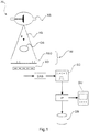
- FIG. 1 there is shown a schematic block diagram of an X-ray imaging apparatus XI (also referred to herein as "imager").
- the X-ray imaging apparatus XI includes an X-ray source XS.
- the detector envisaged is preferably digital, in particular of the flat panel type, but other variants, such as curved ones that are focused on a focal spot of the X-ray source XS, are also envisaged herein.
- an imaging module IM including an X-ray sensitive detector XD.
- the imager is configured to acquire imagery, in particular in relation to an internal structure and/or material composition of the object OB.
- the object OB maybe animate or inanimate.
- the object is a human or animal patient or a part thereof.
- the X-ray imager XI is particularly envisaged for, preferably, spectral imaging in the medical field but other applications in non-medical fields are not excluded herein, such as baggage scanning or non-destructive material testing, etc.
- an object OB to be imaged resides in the examination region between the X-ray source XS and the X-ray detector XD.
- the X-ray source XS is energized by a user through a control unit (not shown).
- the X-ray source XS then emits x-radiation in the form of an X-ray beam XB that traverses the examination region and the object to be imaged.
- the X-ray beam is made up from photons of different energy defined by the spectrum of the x-radiation generated by the X-ray source XS.
- the photons interact with matter in the object OB. Some of the photons are absorbed by the matter whereas other photons emerge at the far side of the object (as viewed from the X-ray source), and then interact with the X-ray sensitive detector XD. Some of the photons that emerge at the far side of the object OB have been scattered because of their interaction with the matter in the object OB whilst other photons emerge unscattered.
- the X-ray imager XI therefore includes an additional component, called an anti-scatter grid ASG, that is part of the image module IM.
- the anti-scatter grid ASG is arranged between the Object OB to be imaged and the detector XD.
- the anti-scatter grid ASG is mounted on top of the detector XD (again then, when viewed from the X-ray source).
- the anti-scatter grid essentially acts as a filter to filter out, by absorption, scattered photons that come from the object. The scattered photons are thus largely prevented from reaching the detector XD.
- the scattered photons are hence largely undetected by the detector thanks to the presence of the ASG.
- it is mainly the unscattered photons that make it through the anti-scatter grid ASG and are then actually detected by the detector XD.
- the unscattered photons are of main interest for imaging.
- the X-ray imager XI as mainly envisaged herein is capable of event counting to quantify the manner in which the photons interact with the detector XD.
- the X-ray imager is a spectral imager that allows spectral analysis of the detected x-radiation/photons. This capability allows for instance a material decomposition of the object. That is, the detected radiation can be analyzed to identify different types of material tissue in the object for instance.
- the anti-scatter grid ASG as proposed herein is of a novel type as it serves a dual function as will be explained in more detail with Figure 2 , but briefly, the newly proposed anti-scatter grid ASG reduces and eliminates scattered photons and, in addition, improves the photon counting capability of the imager XI because if allows to better differentiate signals caused by the photon. This will be explained in more detail below.
- the photons that interact with the X-ray detector XD cause electrical signals which are picked up and processed by a digital acquisition system DAS.
- Conditioning circuitry in the DAS such as pulse shaper, forms these signals into electric pulses which are then passed on to an event counter EC, such as a pulse counter.
- the event counter EC maybe integrated into the imaging module or may be integrated in other components of the imager XI.
- the pulses are quantized or digitized against a set of thresholds. In other words, a height of a given pulse is compared against one, preferably more thresholds, and each time the pulse height exceeds a certain one of the thresholds, a counter is set for this threshold and pulse.
- the electrical signals picked up at the detector XD are converted into a histogram data structure that represents the energy spectrum of the detected photons.
- the histogram data structure allows determining the amount of the detected photons that have energy in a certain energy interval ("bin").
- the energy bins correspond to the thresholds in the event counter EC.
- the so quantized event count data produced at the event counter EC forms raw count data which can be stored in memory or processed by an image processor IP into imagery.
- the imagery may be stored for later reference in an image storage DB or may be rendered for view on the display unit DU.
- the raw data may be processed into spectral imagery where portions of the image correspond to different types of materials that constitute the internals of the imaged object OB.
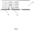
- the detector XD is preferably of the direct convertor type. More particularly, the detector XD includes a direct conversion layer DL formed from a suitable semi-conductor.
- the semiconductors have a crystalline structure, such as Silicon, CdTe, CZT, GaAs and Ge, and others.
- the conversion layer DL is generally of a rectangular shape.
- the conversion layer is sandwiched between pairs of electrodes EL. Only the anodes are shown in the sectional view of Figure 2 , arranged at the distal face of the conversion layer DL.
- the electrodes EL are spaced discretely apart at a distance D ("inter-electrode distance) and in a pattern on the distal surface of the direct conversion layer DL. Each electrode EL has a size d.
- the electrodes EL define a "pixelation" of the otherwise unstructured conversion layer DL. Each electrode EL corresponds to one detector pixel.
- the electrodes EL are sometimes referred to herein as "pixels".
- a voltage is applied across the electrodes and the direct conversion layer DL.
- the cathode is not pixelated to apply the same voltage across the layer DL.
- the anti-scatter grid ASG is mounted on the proximal face of the detection layer DL.
- X-ray photons that pass through the ASG that is, the non-scattered photons
- the ASG that is, the non-scattered photons
- crystals in the detector layer DL Depending on the photon's energy, a number of electrons and holes are released that are otherwise bound in the crystal. The so released electrons and holes may themselves release further electrons and holes.
- Due to the applied voltage a main part of the electrons and the holes cannot recombine and form two respective charge clouds.
- the electron charge cloud defuses (downwardly) towards the anodes EL to cause the earlier mentioned electrical signals.
- the electrical signals are then formed into pulses for the charge clouds and are then processed by the event counter EC as previously described to produce the imagery.
- each electrode pair EL would respond to a charge cloud of a single photon at a time.
- this is not always happening because of a non-negligible finite size of the chare clouds.
- a fraction of the cloud can be directed by the E-field to one of said pixels and another faction is directed to another pixels.
- This fact gives rise to the definition of so called critical zones shown as hatched sections in the cross sectional view of Figure 2 . These critical zones are volume sections inside the conversion layer DL between the electrodes EL.
- the ensuing cloud charge may be registered by two or more, in particular adjacent, electrodes at both side of the respective critical zone CZ.
- This undesirable effect is called "charge sharing".
- the cloud charge induced by a photon through interaction with the direct conversion layer in the critical zones is shared between two or more anodes.
- This charge sharing may cause double or multiple counting for a single given photon because the charge is shared among two or more of the pixels that are defined by the anodes. Charge sharing may therefore disturb the energy discrimination capability of the imager.
- Charge clouds are illustrated as ellipses in the sectional view as per Fig 3 .
- the electrical field generated by the electrodes cause the electrons to travel along trajectories shown as lines in Fig 3 .
- the field lines are curved in the region between the adjacent electrodes which causes curved and diverging trajectories.
- a charge cloud can be described by an average diameter. It can be seen, that the larger the charge cloud, to more likely a charge sharing event is as the electrons in the charge cloud spilt up and are drawn towards on or the other electrode.
- the width of the critical zone is hence a function of the average charge cloud diameter ("ACD").
- the ACD is a quantity than can be determined experimentally, given the type of conversion layer and X-ray spectrum generated by the X-ray source XS.
- the anti-scatter grids arranged on top of the direct conversion layer DL is configured to reduce or even eliminate such multiple counting of the same event.
- this has a grid structure which is also shown in the cross section in Figure 2 .
- a plurality of strips (or lamellae) LAM is arranged side by side with spacers SP to form a surface S that faces the incoming radiation/photons.
- Each of the strips LAM are formed from a highly packed radiation material such as molybdenum, tungsten, lead or other or an alloy of any of these metals.
- the elongated strips have a length which in Figure 2 extends into the paper plane.
- Each strip as a thickness along or parallel to the surface S, and, a "height" which extends outside the surface S and across thereto. Typical heights are between 1-4mm and a typical thickness is about 5-50 ⁇ m, but other dimensions are not excluded herein. In the particular embodiment shown, the heights of the strips extend perpendicular to that surface (so along the main propagation direction of the incoming X-ray beam XB shown as p in Figure 1 ).
- the strips are all parallel and their thickness is perpendicular to the main propagation direction p.
- the surface S of the strips LAM is planar but this not necessary so in all embodiments where the ASG surface S is curved around a point located at the focal spot of source XS. In this manner, focused ASGs may be formed to achieve a higher illumination of the detector.
- the strips LAM are still arranged in a planar surface S as in Fig 2 , but some of the strips LAM are individually rotated or angled around their respective longitudinal axis. The further the strips are situated away from the middle portion of the surface S, the higher the rotation angles are, with no rotation at the center strip.
- the grid includes two types of strips called guard strips L j of which three, L 1 -L 3 are shown, and the remaining scatter strips l 1 -l 6 .
- the two types of strips are arranged in alternation to form the surface S.
- the guard strips referred to generically as “L i ", are thicker than the scatter strips " l i " (to use a similar, generic notation).
- the scatter strips l i are arranged in "runs" or groups of six. In between any two adjacent runs of scatter strips, there is arranged a respective guard strip L i .
- this " ⁇ -1" sequential layout is only exemplary and other layouts (more generally denoted as " 1- N -1", N ⁇ 1) are also envisaged herein.
- the two types of strips and their spatial arrangement implement the previously mentioned double function.
- the scatter strips l i (and that for matter the guard strips L i ) are arranged at a suitable aspect ratio to block scattered photons to so reduce the amount of scatter radiation that reaches the detector layer DL.
- the aspect ratio is an ASG specification and is the ratio between strip height and a distance between two consecutive strips.
- the aspect ratio defines the acceptance angle and hence the proportion of photons that are allowed to pass the ASG.
- the aspect ratio may be a function of the mean energy of the X-radiation/photon emitted from the X-ray source XS.
- the thicker guard strips L are arranged to reduce charge sharing and thus the likelihood of multiple counts for a single photon interaction event. Specifically, the charge sharing reduction capability of the guard strips Lj comes about because their thickness corresponds to the width D of the critical zones CZ.
- the guard strip thickness is about the size of the ACD.
- the ACD may be less than the inter-electrode distance D or it may be about equal. Consequently, the guard strip is less or equal D.
- the thickness may be chosen accordingly although it is envisaged herein to "clip" the guard strip thickness at about D or about 1.5 x D to avoid undue degradation of the DQE.
- a DQE of about 80% should be considered although there maybe good reasons to drop this restriction in some cases.
- the guard strips L i are so aligned that, when viewed in plan view from the X-ray source XS, the guard strips are situated on top of the critical zones CZ in between any two adjacent electrodes EL. Due to their tuned thickness and their positioning in between the electrodes (in plan view) the guard strips L i essentially prevent incoming photons from reaching the critical zones CZ in the direct conversion layer. The formation of charge clouds that may cause multiple counts events can thus be prevented.
- a respective spacer SP strip formed from a suitable, radiation-translucent filler material.
- suitable filler materials include cellulose such as paper, plastics or glues.
- the whole of the strips LAM are embedded, partly or completely, in a filler matrix or filler material package.
- the spacers SP add integrity and stability by making the ASG resistant to shearing or other deformation and define the inter-spaces d between the strips to form "channels" to allow the non-scattered photons pass.
- the size and shape of the ASG usually comports to the shape and size of the X-ray detector XD on which the ASG is to be permanently or releasable mounted. In the embodiment where the detector XD is of the flat panel type, the ASG is then of equal, rectangular shape to match the shape and size of the radiation receiving face of the X-ray detector XD.
- the thickness of the guard strips is a function of the ACD and hence the width of the critical zones CZ which are to be covered by the guard strips.
- some or all of the guard strips L i may be substantially as thick as the critical zones are wide.
- some or all of the guard strips L i may be slightly thicker than the critical zone width.
- the number of scatter strips l i in each block depends on the size d of the electrodes.
- the thickness of the guard strips corresponds to the width of the critical zone CZ / ACD
- the number of scatter strips that are arranged in a run correspond to the size of the anode EL.
- the block of contiguous strips l i may be substantially as long as the pixel is wide or slightly longer.
- the center line of the guard strips should preferably coincide with the center line through the inter-electrode distance D, with the guard strip extending either side of the center lines by ACD/2.
- the guard strips L j have the same thickness and there are the same number of scatter strips l i used in each run.
- the guard strips may be 4 or 5 times thicker than the scatter strips.
- the ASG is mainly envisaged to form a one dimensional ("1D") grid as shown in Figure 2 .
- all strips LAM are essentially parallel with no strip running in a direction across.
- two-dimensional (“2D") grids are also envisaged herein where the inter-strip spaces filled by the spacer material SP form a checkerboard pattern.
- this type of ASG consists of two sets of strips each forming a 1D grid as in Fig 2 , with the two sets crossing each other at 90°.
- 2D grid can be built from two 1D grids as per Figure 2 .
- the two 1D grids are arranged on top of each other at 90° to form a layered structure, the desired2D ASG.
- the ASG maybe arranged with a 1D strip pattern.
- the ASG may instead have a 2D strip pattern where the strips are arranged in two sets of directions perpendicular to each other.
- charge sharing can be reduced in one direction only (namely in the direction across the strips).
- charge sharing can be reduced in two directions perpendicular to each other.
- An exemplary width D of the critical zone is about 40 ⁇ m.
- the thickness of the guard strips is equally about 40 ⁇ m.
- the spacer thickness is a function of ( s,c,N, t ) given a required DQE (detective quantum efficiency).
- the profile-height in turn is a function of the spacer thickness and aspect ratio.
- Typical pixel sizes envisaged herein are between 50 ⁇ m and 1 mm.
- Typical foil thickness of strips ( l i ) are between 5 ⁇ m to 50 ⁇ m whilst foil thicknesses of the guard strips ( L i ) are about 20 ⁇ m to 200 ⁇ m.
- One method of manufacture of the above described ASG of the 1D type as envisaged herein is to form the strips from metallic foil.
- the foils may be readily cold rolled into the desired thickness and suitably sized by slitting and trimming. Pack rolling may be done to increase throughput.
- the thicker metal foil may be formed by gluing or otherwise affixing multiple layers of the available foil sheet.
- the foil for the guard strip may be formed from multiple layer of the thinner, foil for the scatter strips. Using foils for forming the strips has been found to be low-cost.
- the sheets of foil of greater thicknesses for the guard strips and the other, thinner sheets of foil for the scatter strips are arranged one on top of each other in a stack, with any two sheets of foil having a layer of spacer material SP interposed in between.
- the thicker and thinner foil sheets are arranged in suitable alteration to achieve the desired sequential pattern 1-N-1, with N ( ⁇ 1) thin foils arranged in respective sub-stacks, with a thick foil for the guard strip arranged in between any two such sub-stacks.
- N ( ⁇ 1) thin foils arranged in respective sub-stacks
- a thick foil for the guard strip arranged in between any two such sub-stacks.
- the spacer material layers are glued or otherwise affixed between the two neighboring layers of metallic foil L j ,, l i .
- the whole layered stack of metallic foil and spacer material is then left to cure if glue is used.
- slices are cut through the stack. The section plane is perpendicular to faces of the foil sheets in the stack. Each slice then corresponds to an ASG as envisaged herein, with each such stack yielding a plurality of ASGs.
- a stabilizing frame may be run around the edges of the ASG structures so formed.
- the metallic material for the foils used for the scatter strips and the guard strips, respectively may not be the same.
- more expensive or higher density or radiation opacity material may be used for the guard strips L i as opposed to cheaper or less dense, less radiation-opaque material for the scatter strips l i .
- the same foil is used in different thickness for scatter strips l i and guard strips L j .
- a 2D variant of the ASG is required, two such 1D ASG may be placed and affixed on top of other, with one of the rotated by 90° relative to each other.
- the 2D ASG variant has twice the profile-height of the 1D ASG.
- the detector XD as described above is of the direct conversion type
- indirect type converters which use an additional layer, a scintillator
- the scintillator layer comprises a plurality of comparably small, active light guides or "pipes".
- Caesium Iodide (CsI) is grown in columnar 'needle-like' structures. Each column of CsI acts as a light pipe directing the visible light photons received from the scintillator to a light detector (e.g., a photo diode).
- the light can be shared between adjacent pixels as the light photons will have a certain spread when emanating from the scintillator layer.
- the spread may be geometrically described by a cone with a certain apex angle. This photon-based effect is comparable to the effect of charge sharing in detectors using direct conversion materials as explained above.
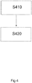
- an average charge cloud diameter is determined for a given conversion layer DL type. This can be done experimentally by scanning a pencil X-radiation beam over the detector. An aperture mask or collimator may be used to realize the pencil beam. For each position of the beam at a given pixel, the responses of neighboring pixels are determined. With distance from the beam, the measured number of counts per time unit will drop under a given threshold (e.g. to zero). If this happens, the distance will provide a good approximation for the ACD. The procedure is repeated at different sample locations throughout the detector layer. The ACD values so gotten may then be averaged to obtain the ACD.
- a given threshold e.g. to zero
- the thickness of the guard strip (Li) is specified at step S420 and this can be used to prepare a foil of suitable thickness and proceed to build the ASG, for instance according to the stack layering technique as described above.
- the "conversion layer” in this case is the scintillator layer that converts X-ray into light rather than the conversion layer DL discussed above which converts X-ray into charge.
- the quantity measured at step S420 is an average spread of light photons generated in the scintillator.
- foil-layering method alternatives such as sputtering or other layer depositing techniques are also envisaged in alternative embodiments.
Landscapes
- Physics & Mathematics (AREA)
- Health & Medical Sciences (AREA)
- High Energy & Nuclear Physics (AREA)
- Spectroscopy & Molecular Physics (AREA)
- Life Sciences & Earth Sciences (AREA)
- General Physics & Mathematics (AREA)
- Molecular Biology (AREA)
- Engineering & Computer Science (AREA)
- General Engineering & Computer Science (AREA)
- Pulmonology (AREA)
- Nuclear Medicine, Radiotherapy & Molecular Imaging (AREA)
- Radiology & Medical Imaging (AREA)
- Theoretical Computer Science (AREA)
- Chemical & Material Sciences (AREA)
- Analytical Chemistry (AREA)
- Biochemistry (AREA)
- General Health & Medical Sciences (AREA)
- Immunology (AREA)
- Pathology (AREA)
- Measurement Of Radiation (AREA)
- Apparatus For Radiation Diagnosis (AREA)
- Analysing Materials By The Use Of Radiation (AREA)
Priority Applications (6)
| Application Number | Priority Date | Filing Date | Title |
|---|---|---|---|
| EP17186194.1A EP3444826A1 (de) | 2017-08-14 | 2017-08-14 | Niederprofil-antistreu- und anti-ladungsverteilungsgitter für photonenzählungs-computertomografie |
| CN201880062054.7A CN111133532B (zh) | 2017-08-14 | 2018-08-14 | 用于光子计数计算机断层摄影的低轮廓防散射和防电荷共享光栅 |
| PCT/EP2018/072018 WO2019034650A1 (en) | 2017-08-14 | 2018-08-14 | ANTI-DISPERSAL GRID AND LOW PROFILE LOAD DISPERSION FOR TOMODENSITOMETRY WITH PHOTON COUNTING |
| EP18752496.2A EP3669381A1 (de) | 2017-08-14 | 2018-08-14 | Niederprofil-antistreu- und anti-ladungsverteilungsgitter für photonenzählungs-computertomografie |
| JP2020507557A JP7118133B2 (ja) | 2017-08-14 | 2018-08-14 | 光子カウントコンピュータ断層撮影のための薄型散乱防止及び電荷共有防止グリッド、当該グリッドを有する撮像装置、当該グリッドの製造方法 |
| US16/637,876 US11152129B2 (en) | 2017-08-14 | 2018-08-14 | Low profile anti scatter and anti charge sharing grid for photon counting computed tomography |
Applications Claiming Priority (1)
| Application Number | Priority Date | Filing Date | Title |
|---|---|---|---|
| EP17186194.1A EP3444826A1 (de) | 2017-08-14 | 2017-08-14 | Niederprofil-antistreu- und anti-ladungsverteilungsgitter für photonenzählungs-computertomografie |
Publications (1)
| Publication Number | Publication Date |
|---|---|
| EP3444826A1 true EP3444826A1 (de) | 2019-02-20 |
Family
ID=59677043
Family Applications (2)
| Application Number | Title | Priority Date | Filing Date |
|---|---|---|---|
| EP17186194.1A Withdrawn EP3444826A1 (de) | 2017-08-14 | 2017-08-14 | Niederprofil-antistreu- und anti-ladungsverteilungsgitter für photonenzählungs-computertomografie |
| EP18752496.2A Pending EP3669381A1 (de) | 2017-08-14 | 2018-08-14 | Niederprofil-antistreu- und anti-ladungsverteilungsgitter für photonenzählungs-computertomografie |
Family Applications After (1)
| Application Number | Title | Priority Date | Filing Date |
|---|---|---|---|
| EP18752496.2A Pending EP3669381A1 (de) | 2017-08-14 | 2018-08-14 | Niederprofil-antistreu- und anti-ladungsverteilungsgitter für photonenzählungs-computertomografie |
Country Status (5)
| Country | Link |
|---|---|
| US (1) | US11152129B2 (de) |
| EP (2) | EP3444826A1 (de) |
| JP (1) | JP7118133B2 (de) |
| CN (1) | CN111133532B (de) |
| WO (1) | WO2019034650A1 (de) |
Families Citing this family (1)
| Publication number | Priority date | Publication date | Assignee | Title |
|---|---|---|---|---|
| US11320545B2 (en) * | 2020-07-07 | 2022-05-03 | GE Precision Healthcare LLC | Systems and methods for improved medical imaging |
Citations (2)
| Publication number | Priority date | Publication date | Assignee | Title |
|---|---|---|---|---|
| US20050111627A1 (en) * | 2003-11-21 | 2005-05-26 | Juergen Leppert | Method of shielding scattered radiation in front of a detector array |
| US20130168567A1 (en) * | 2011-12-28 | 2013-07-04 | General Electric Company | Collimator for a pixelated detector |
Family Cites Families (31)
| Publication number | Priority date | Publication date | Assignee | Title |
|---|---|---|---|---|
| US4875227A (en) * | 1986-12-06 | 1989-10-17 | Rossi Remo J | Anti-scatter grid system |
| FR2830976B1 (fr) | 2001-10-17 | 2004-01-09 | Ge Med Sys Global Tech Co Llc | Grilles anti-diffusantes a faible attenuation et procede de fabrication de telles grilles |
| DE10202987A1 (de) | 2002-01-26 | 2003-07-31 | Philips Intellectual Property | Gitter zur Absorption von Röntgenstrahlung |
| SE524731C2 (sv) * | 2002-06-07 | 2004-09-21 | Xcounter Ab | Metod och apparat för detektering av joniserande strålning |
| US7072446B2 (en) | 2003-05-13 | 2006-07-04 | Analogic Corporation | Method for making X-ray anti-scatter grid |
| EP1815270A2 (de) * | 2004-07-14 | 2007-08-08 | Orbotech Medical Solutions Ltd. | Strahlungsdetektor-kopf |
| WO2006018779A2 (en) | 2004-08-12 | 2006-02-23 | Philips Intellectual Property & Standards Gmbh | Anti-scatter-grid for a radiation detector |
| WO2008059425A2 (en) * | 2006-11-17 | 2008-05-22 | Koninklijke Philips Electronics N.V. | Radiation detector with multiple electrodes on a sensitive layer |
| US7486764B2 (en) * | 2007-01-23 | 2009-02-03 | General Electric Company | Method and apparatus to reduce charge sharing in pixellated energy discriminating detectors |
| US20090008564A1 (en) * | 2007-07-05 | 2009-01-08 | Cmt Medical Technologies Ltd. | Modular X-Ray Detector With Single Photon Counting, Energy Sensitivity And Integration Capabilities |
| DE102009031481A1 (de) * | 2008-07-03 | 2010-02-11 | Ohnesorge, Frank, Dr. | Konzept für optische (Fernfeld-/Fresnel-Regime aber auch Nahfeld-) Mikroskopie/Spektroskopie unterhalb/jenseits des Beugungslimits - Anwendungen für optisches (aber auch elektronisches) schnelles Auslesen von ultrakleinen Speicherzellen in Form von lumineszierenden Quantentrögen - sowie in der Biologie/Kristallographie |
| JP4715974B2 (ja) | 2008-07-22 | 2011-07-06 | 株式会社島津製作所 | 散乱線除去グリッドの製造方法 |
| US8411823B2 (en) | 2008-08-11 | 2013-04-02 | Shimadzu Corporation | Radiation grid and radiographic apparatus provided with the same |
| US8183535B2 (en) * | 2009-02-11 | 2012-05-22 | Mats Danielsson | Silicon detector assembly for X-ray imaging |
| JP6353361B2 (ja) * | 2011-07-04 | 2018-07-04 | コーニンクレッカ フィリップス エヌ ヴェKoninklijke Philips N.V. | 位相コントラストイメージング装置 |
| IN2014CN01055A (de) * | 2011-08-30 | 2015-04-10 | Koninkl Philips Nv | |
| US9135728B2 (en) * | 2012-04-04 | 2015-09-15 | General Electric Company | System and method for multi-energy computed tomography imaging |
| CN104569002B (zh) * | 2013-10-23 | 2018-04-27 | 北京纳米维景科技有限公司 | 基于光子计数的x射线相衬成像系统、方法及其设备 |
| JP6247423B2 (ja) * | 2014-08-05 | 2017-12-13 | コーニンクレッカ フィリップス エヌ ヴェKoninklijke Philips N.V. | X線イメージング装置用のグレーティング装置 |
| US20160206255A1 (en) * | 2015-01-16 | 2016-07-21 | Kabushiki Kaisha Toshiba | Hybrid passive/active multi-layer energy discriminating photon-counting detector |
| JP6470986B2 (ja) * | 2015-01-28 | 2019-02-13 | ジーイー・メディカル・システムズ・グローバル・テクノロジー・カンパニー・エルエルシー | 放射線検出器及び放射線断層撮影装置 |
| US9993220B2 (en) * | 2015-06-26 | 2018-06-12 | Prismatic Sensors Ab | Scatter estimation and/or correction in x-ray imaging |
| US10267928B2 (en) * | 2015-11-26 | 2019-04-23 | Koninklijke Philips N.V. | Dark current compensation |
| CN108291974B (zh) * | 2015-12-03 | 2022-08-09 | 皇家飞利浦有限公司 | 辐射探测器和成像装置 |
| JP6456854B2 (ja) * | 2016-01-12 | 2019-01-23 | 株式会社日立製作所 | 放射線撮像装置 |
| CN109983542B (zh) | 2016-11-24 | 2023-09-01 | 皇家飞利浦有限公司 | 用于探测器装置的防散射网格组件 |
| US10222489B2 (en) * | 2017-03-13 | 2019-03-05 | General Electric Company | Pixel-design for use in a radiation detector |
| US11224389B2 (en) * | 2017-04-17 | 2022-01-18 | The Regents Of The University Of Colorado, A Body Corporate | Radiation transmission grid apparatus and methods for x-ray imaging detectors |
| US10779778B2 (en) * | 2017-05-08 | 2020-09-22 | General Electric Company | Reference detector elements in conjunction with an anti-scatter collimator |
| US10610191B2 (en) * | 2017-07-06 | 2020-04-07 | Prismatic Sensors Ab | Managing geometric misalignment in x-ray imaging systems |
| WO2020106197A1 (en) * | 2018-11-19 | 2020-05-28 | Prismatic Sensors Ab | X-ray imaging system for phase contrast imaging using photon-counting events |
-
2017
- 2017-08-14 EP EP17186194.1A patent/EP3444826A1/de not_active Withdrawn
-
2018
- 2018-08-14 WO PCT/EP2018/072018 patent/WO2019034650A1/en unknown
- 2018-08-14 JP JP2020507557A patent/JP7118133B2/ja active Active
- 2018-08-14 US US16/637,876 patent/US11152129B2/en active Active
- 2018-08-14 EP EP18752496.2A patent/EP3669381A1/de active Pending
- 2018-08-14 CN CN201880062054.7A patent/CN111133532B/zh active Active
Patent Citations (2)
| Publication number | Priority date | Publication date | Assignee | Title |
|---|---|---|---|---|
| US20050111627A1 (en) * | 2003-11-21 | 2005-05-26 | Juergen Leppert | Method of shielding scattered radiation in front of a detector array |
| US20130168567A1 (en) * | 2011-12-28 | 2013-07-04 | General Electric Company | Collimator for a pixelated detector |
Also Published As
| Publication number | Publication date |
|---|---|
| WO2019034650A1 (en) | 2019-02-21 |
| JP2020530903A (ja) | 2020-10-29 |
| US20200251236A1 (en) | 2020-08-06 |
| CN111133532B (zh) | 2023-11-17 |
| EP3669381A1 (de) | 2020-06-24 |
| JP7118133B2 (ja) | 2022-08-15 |
| CN111133532A (zh) | 2020-05-08 |
| US11152129B2 (en) | 2021-10-19 |
Similar Documents
| Publication | Publication Date | Title |
|---|---|---|
| US7486764B2 (en) | Method and apparatus to reduce charge sharing in pixellated energy discriminating detectors | |
| US7606347B2 (en) | Photon counting x-ray detector with overrange logic control | |
| JP5215722B2 (ja) | オーバーレンジ論理制御を伴う光子計数x線検出器 | |
| CN100486524C (zh) | 计算机断层摄影检测器制造过程 | |
| US7570736B2 (en) | Direct conversion energy discriminating CT detector with over-ranging correction | |
| US7696481B2 (en) | Multi-layered detector system for high resolution computed tomography | |
| AU743023B2 (en) | A method and a device for planar beam radiography and a radiation detector | |
| Shikhaliev | Tilted angle CZT detector for photon counting/energy weighting x-ray and CT imaging | |
| US7589327B2 (en) | Energy sensitive direct conversion radiation detector | |
| EP2675358B1 (de) | Detektoranordnung mit effektiver grösse über der tatsächlichen grösse | |
| US7734017B2 (en) | Anti-scatter-grid for a radiation detector | |
| EP2356485B1 (de) | Strahlungsdetektor mit einem elektrodenarray | |
| CN112262326B (zh) | x射线检测器设计 | |
| US20160206255A1 (en) | Hybrid passive/active multi-layer energy discriminating photon-counting detector | |
| US11152129B2 (en) | Low profile anti scatter and anti charge sharing grid for photon counting computed tomography | |
| EP1802998B1 (de) | Nuklearmedizinischer detektor | |
| CN219810870U (zh) | 多层x射线探测器 | |
| JP2023168246A (ja) | X線検出器用コリメータアセンブリ | |
| DE102016107638A1 (de) | Röntgenzeilendetektor, verwendung eines röntgendetektors, dualer röntgendetektor und röntgenzeilendetektor-anordnung |
Legal Events
| Date | Code | Title | Description |
|---|---|---|---|
| PUAI | Public reference made under article 153(3) epc to a published international application that has entered the european phase |
Free format text: ORIGINAL CODE: 0009012 |
|
| AK | Designated contracting states |
Kind code of ref document: A1 Designated state(s): AL AT BE BG CH CY CZ DE DK EE ES FI FR GB GR HR HU IE IS IT LI LT LU LV MC MK MT NL NO PL PT RO RS SE SI SK SM TR |
|
| AX | Request for extension of the european patent |
Extension state: BA ME |
|
| STAA | Information on the status of an ep patent application or granted ep patent |
Free format text: STATUS: THE APPLICATION IS DEEMED TO BE WITHDRAWN |
|
| 18D | Application deemed to be withdrawn |
Effective date: 20190821 |