US20090008564A1 - Modular X-Ray Detector With Single Photon Counting, Energy Sensitivity And Integration Capabilities - Google Patents
Modular X-Ray Detector With Single Photon Counting, Energy Sensitivity And Integration Capabilities Download PDFInfo
- Publication number
- US20090008564A1 US20090008564A1 US11/773,450 US77345007A US2009008564A1 US 20090008564 A1 US20090008564 A1 US 20090008564A1 US 77345007 A US77345007 A US 77345007A US 2009008564 A1 US2009008564 A1 US 2009008564A1
- Authority
- US
- United States
- Prior art keywords
- ray
- photodiode
- detector
- charge
- electronic circuit
- Prior art date
- Legal status (The legal status is an assumption and is not a legal conclusion. Google has not performed a legal analysis and makes no representation as to the accuracy of the status listed.)
- Abandoned
Links
- 230000010354 integration Effects 0.000 title description 11
- 230000035945 sensitivity Effects 0.000 title description 2
- 230000005855 radiation Effects 0.000 claims abstract description 21
- 238000006243 chemical reaction Methods 0.000 claims description 10
- NJPPVKZQTLUDBO-UHFFFAOYSA-N novaluron Chemical compound C1=C(Cl)C(OC(F)(F)C(OC(F)(F)F)F)=CC=C1NC(=O)NC(=O)C1=C(F)C=CC=C1F NJPPVKZQTLUDBO-UHFFFAOYSA-N 0.000 claims description 6
- 230000007246 mechanism Effects 0.000 claims description 4
- 239000000758 substrate Substances 0.000 description 12
- 239000000463 material Substances 0.000 description 9
- 238000000034 method Methods 0.000 description 9
- 238000001514 detection method Methods 0.000 description 5
- 238000003491 array Methods 0.000 description 4
- 230000008901 benefit Effects 0.000 description 4
- 230000000875 corresponding effect Effects 0.000 description 4
- 239000004593 Epoxy Substances 0.000 description 3
- WXNXCEHXYPACJF-ZETCQYMHSA-N N-acetyl-L-leucine Chemical compound CC(C)C[C@@H](C(O)=O)NC(C)=O WXNXCEHXYPACJF-ZETCQYMHSA-N 0.000 description 3
- BQCADISMDOOEFD-UHFFFAOYSA-N Silver Chemical compound [Ag] BQCADISMDOOEFD-UHFFFAOYSA-N 0.000 description 3
- 238000013459 approach Methods 0.000 description 3
- 238000003384 imaging method Methods 0.000 description 3
- 238000005259 measurement Methods 0.000 description 3
- 230000008569 process Effects 0.000 description 3
- 229910052709 silver Inorganic materials 0.000 description 3
- 239000004332 silver Substances 0.000 description 3
- RYGMFSIKBFXOCR-UHFFFAOYSA-N Copper Chemical compound [Cu] RYGMFSIKBFXOCR-UHFFFAOYSA-N 0.000 description 2
- 229910052802 copper Inorganic materials 0.000 description 2
- 239000010949 copper Substances 0.000 description 2
- 238000002059 diagnostic imaging Methods 0.000 description 2
- 238000005516 engineering process Methods 0.000 description 2
- 230000003287 optical effect Effects 0.000 description 2
- 229910052710 silicon Inorganic materials 0.000 description 2
- 239000010703 silicon Substances 0.000 description 2
- ZCYVEMRRCGMTRW-UHFFFAOYSA-N 7553-56-2 Chemical compound [I] ZCYVEMRRCGMTRW-UHFFFAOYSA-N 0.000 description 1
- 239000004642 Polyimide Substances 0.000 description 1
- ATJFFYVFTNAWJD-UHFFFAOYSA-N Tin Chemical compound [Sn] ATJFFYVFTNAWJD-UHFFFAOYSA-N 0.000 description 1
- 229910052797 bismuth Inorganic materials 0.000 description 1
- JCXGWMGPZLAOME-UHFFFAOYSA-N bismuth atom Chemical compound [Bi] JCXGWMGPZLAOME-UHFFFAOYSA-N 0.000 description 1
- 229910052792 caesium Inorganic materials 0.000 description 1
- TVFDJXOCXUVLDH-UHFFFAOYSA-N caesium atom Chemical compound [Cs] TVFDJXOCXUVLDH-UHFFFAOYSA-N 0.000 description 1
- 239000003990 capacitor Substances 0.000 description 1
- 230000015556 catabolic process Effects 0.000 description 1
- 239000000919 ceramic Substances 0.000 description 1
- 230000001427 coherent effect Effects 0.000 description 1
- 239000004020 conductor Substances 0.000 description 1
- 230000002596 correlated effect Effects 0.000 description 1
- 230000008878 coupling Effects 0.000 description 1
- 239000007822 coupling agent Substances 0.000 description 1
- 238000010168 coupling process Methods 0.000 description 1
- 238000005859 coupling reaction Methods 0.000 description 1
- 230000002950 deficient Effects 0.000 description 1
- 238000006731 degradation reaction Methods 0.000 description 1
- 229920005994 diacetyl cellulose Polymers 0.000 description 1
- 230000004907 flux Effects 0.000 description 1
- 229910052740 iodine Inorganic materials 0.000 description 1
- 239000011630 iodine Substances 0.000 description 1
- 230000005865 ionizing radiation Effects 0.000 description 1
- 238000004519 manufacturing process Methods 0.000 description 1
- 230000000873 masking effect Effects 0.000 description 1
- 229910052751 metal Inorganic materials 0.000 description 1
- 239000002184 metal Substances 0.000 description 1
- 238000000386 microscopy Methods 0.000 description 1
- 238000012986 modification Methods 0.000 description 1
- 230000004048 modification Effects 0.000 description 1
- 239000011368 organic material Substances 0.000 description 1
- 238000005498 polishing Methods 0.000 description 1
- 229920003223 poly(pyromellitimide-1,4-diphenyl ether) Polymers 0.000 description 1
- 229920001721 polyimide Polymers 0.000 description 1
- 238000002601 radiography Methods 0.000 description 1
- 238000002310 reflectometry Methods 0.000 description 1
- 230000000717 retained effect Effects 0.000 description 1
- 238000005476 soldering Methods 0.000 description 1
- 239000007787 solid Substances 0.000 description 1
- 230000003595 spectral effect Effects 0.000 description 1
- 238000003325 tomography Methods 0.000 description 1
- 238000012546 transfer Methods 0.000 description 1
- 239000013598 vector Substances 0.000 description 1
Images


Classifications
-
- G—PHYSICS
- G01—MEASURING; TESTING
- G01T—MEASUREMENT OF NUCLEAR OR X-RADIATION
- G01T1/00—Measuring X-radiation, gamma radiation, corpuscular radiation, or cosmic radiation
- G01T1/16—Measuring radiation intensity
- G01T1/161—Applications in the field of nuclear medicine, e.g. in vivo counting
- G01T1/164—Scintigraphy
- G01T1/1641—Static instruments for imaging the distribution of radioactivity in one or two dimensions using one or several scintillating elements; Radio-isotope cameras
- G01T1/1644—Static instruments for imaging the distribution of radioactivity in one or two dimensions using one or several scintillating elements; Radio-isotope cameras using an array of optically separate scintillation elements permitting direct location of scintillations
Definitions
- the present invention relates to ionizing radiation sensors. More particularly, the present invention relates to a hybrid modular X-ray detector capable of single photon counting (SPC) and charge (signal) integration.
- SPC single photon counting
- signal signal
- Imaging of the human body in medical applications is often achieved by detection of X-rays in scintillating materials, in which each X-ray photon is converted into a large number of visible photons.
- the visible photons are further transferred to an attached photo-detector (PD), which produces an electrical signal.
- the signal is due to the arrival of a single X-ray photon (single photon counting—SPC).
- SPC single photon counting
- a PD output signal is a measure of the total energy generated by the incident photon.
- the PD output signal reflects the integrated charge due to the arrival of several X-ray photons within a preset time interval.
- Imaging requires the measurement of two-dimensional X-ray intensity distribution. This is commonly achieved by the use of position sensitive detectors.
- General radiography detectors use non-pixelated scintillator elements. Most such detectors use column-grown scintillator layers
- detector arrays are built by coupling pixelated arrays of scintillator elements to respective arrays of photodiode elements. Scattered X-ray radiation leads to strong degradation of image quality; to restore image quality one has to use antiscatter grids and also to increase the radiation dose exposure.
- Non-metallic septa between detector elements are used in existing pixelated scintillators to improve the light collection by the photodiode elements.
- the role of the septa is to confine visible light photons close to the location where the X-ray photon was stopped.
- a problem may arise from small signals (smaller than a LOW threshold) generated by some photons. These photons are not accounted for, introducing an error.
- the LOW threshold is typically equivalent to about 700-1000 electrons (lower is better, limited by electronic noise).
- a HIGH threshold is typically equivalent to ⁇ 2000 electrons
- Some of the X-ray photons that enter the scintillator are stopped within a scintillator cell. For each, at least part of the photon energy is retained within the scintillator cell and generates a stream of visible photons; the remaining energy is either emitted outside the scintillator volume (and does not contribute to the detection process) or reaches neighboring scintillator cells (the latter known as “signal sharing”). Most visible photons make their way to the PD cell attached to the scintillator cell; they are stopped and generate an electrical current.
- SPC involves short duration (slightly more than the duration of the current generated by the arrival of an X-ray photon; for a CsI (Tl) scintillator ⁇ 8 microseconds).
- the resulting voltage pulse (which is a measure of the total charge) is compared with a preset threshold exemplarily equivalent to a total charge of 700 electrons. Pulses with amplitude higher than the threshold are representative of detection of an X-ray photon and are counted.
- the advantages and weaknesses of SPC in conjunction with indirect photon detection recommend SPC be used only for low photon fluence (low radiation dose).
- SPC advantages include counting all photons with associated-signals above the threshold and possibility to extract coarse spectral information (one assumes that larger signals indicate photons with higher energy) through use of several thresholds.
- SPC disadvantages include: a) the need for threshold values to be high enough to prevent counting noise signals (low noise electronic circuitry is required; typical noise standard-deviation values are equivalent to about 70-300 electrons). The presence of very-small signals and the need to prevent noise counting leads to failure to detect photons that generate small-amplitude pulses; b) a lack of one-to-one correspondence between the signal-amplitude and the X-ray photon energy. Photons of a given energy may generate a larger signal or a smaller signal (e.g.
- a 45 keV photon stopped within a scintillator cell may transfer the whole energy or only 15 keV to this cell, the latter due to the escape of a 30 keV fluorescence photon; also, there is a large spread in the amount of light generated in the scintillator cell, transferred to the PD and converted into charge).
- the associated-signal may be lower than the preset (e.g. ca. 700 electrons) threshold, such that the respective photon is missed/not counted; and c) “Pile-up”, i.e. the arrival of several X-ray photons within a small time-interval that cannot be properly handled.
- the respective pulses overlap, resulting in generation of a number of counts smaller than the actual number of photons stopped in the scintillator-cell.
- Charge integration involves long duration (typical time: 5 to 30 milliseconds). Within this time, a few to several thousand X-ray photons are sensed and the electric-charge released as they are stopped is collected, stored (typically on a capacitor) and measured. The result is seen as a measure of the number of X-ray photons stopped in the scintillator cell.
- Charge-integration advantages include all signals being included in or contributing to the final measurement, whether the signal-amplitude is small or large, and the fact that pile-up situations cause no ambiguities or errors.
- Charge-integration disadvantages include contribution of electronic-noise to the final signal, and the fact that the final signal may be an inaccurate measure of the photon-number: photons that generate signals with higher amplitude contribute more than photons (mostly low-energy photons) that generate signals of lower-amplitude.
- a typical parameter that characterizes image quality is the signal to noise ratio SNR.
- SNR signal to noise ratio
- the present invention discloses devices, systems and methods for detecting X-ray radiation and forming an image therefrom
- the invention discloses a hybrid modular X-ray detector capable of SPC and charge integration.
- the detector is in essence an indirect conversion sensor (i.e. the X-ray radiation is first converted into light photons and then into electrical charge) based on a pixelated scintillator array.
- the basic detector module includes an antiscatter-grid, a pixelated scintillator, a back-illuminated diode array and an array of dedicated electronics-cells associated with each scintillator-diode pair.
- an indirect conversion X-ray radiation sensor system comprising a plurality of detector modules for detecting X-ray radiation from a radiation source, each module having a module axis, the modules arranged with individual pedestals in a staggered configuration wherein the module axis points to the X-ray radiation source.
- an X-ray radiation sensor comprising a plurality of detector modules configured to perform indirect conversion and concurrent single photon counting and charge-integration of the X-ray radiation, wherein each detector module is mounted on a separate tilting mechanism and wherein the tilting mechanisms are arranged in a staggered configuration
- FIG. 1 shows a basic detector module of the present invention
- FIG. 2A shows an embodiment of a staggered detector module configuration
- FIG. 2B shows details of a detector module mounted on a tilting pedestal
- FIG. 2C shows the problem of masking in modules not pointing directly to an X-ray source
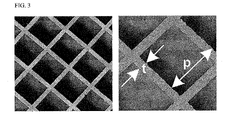
- FIG. 3 shows microscopy pictures of septa used in a detector module of the present invention
- FIG. 4 shows schematics of the electronic circuitry for a single detector channel.
- FIG. 1 shows a basic detector module 100 of the present invention.
- Module 100 comprises several layers: an optional anti-scatter grid layer 102 having anti-scatter cells 112 , a pixelated scintillator layer 104 having scintillator pixels 114 , a photodiode (PD) array layer 106 , a substrate 107 and an electronics layer 108 arranged as shown.
- the pixilated scintillator layer includes “cells” comprised of the scintillator material and metal septa walls 105 .
- a scintillator cell may exemplarily include CsI (Tl) as a scintillator material, surrounded by five (four sides and a top) highly reflecting Silver or Silver-plated Copper septa walls.
- a sixth (bottom) wall is transparent. Exemplary septa pictures are shown in FIG. 3 .
- PD array layer 106 includes an array of preferably back-illuminated photodiodes 116 , which are registered with pixels 114 and, when present, with cells 112 . Each PD is below the transparent scintillator cell floor and receives the radiated visible photons as an X-ray photon is absorbed in the scintillator. The PD absorbs the visible light and generates an electrical current.
- Substrate layer 107 e.g. a printed circuit board or “PCB” is fixedly attached to the diode array layer by e.g. soldering and includes connecting paths 117 registered with diodes 116 . Paths 117 are generally electrical conductors that carry current from PDs to respective amplifiers included in an electronic circuit 118 .
- a column formed of elements 112 , 114 , 116 , 117 and 118 is considered a “detector element” or “channel” 150 .
- each comprises its own elements 112 , 114 , 116 , 117 and 118 .
- 64 channels are sacrificed so that the corresponding diodes are used as electrical connectors and apply bias to the PD array back surface (the light entry surface).
- Circuit 118 integrates the current supplied by each diode as a photon is detected and then measures the charge by comparison with thresholds, see below.
- Layer 108 can be implemented for example as an application specific integrated circuit (ASIC), which is described in more detail below. Layer 108 is typically soldered to the substrate.
- ASIC application specific integrated circuit
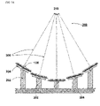
- FIG. 2A shows an embodiment of a staggered detector module system 200 .
- System 200 includes a plurality (five are shown) of detector modules 100 , each module mounted on its own tilting pedestal 202 (see also FIG. 2B ).
- the pedestals may have different heights.
- a pedestal 202 includes a tilt plate 204 for fixedly attaching the detector module and a base 208 .
- Tilt plate 204 may be tilted through a predetermined angle range.
- the different modules in a system 200 are each tilted so that a vertical module axis 206 points towards an X-ray source focal point 210 . As shown in FIG. 2C , this configuration prevents passage and attenuation of photons through adjacent scintillator cells (pixels) and the separating walls.
- FIG. 2C shows a detector module in two different positions I and II relative to an X-ray photon trajectory 220 .
- position I detector axis 206 is non-parallel to trajectory 220 .
- position II detector axis 206 is parallel to trajectory 220 .
- X-ray photons moving along trajectory 220 cross both cells A and B. That is, a fraction of the photon flux headed to pixel B is stopped in pixel A and in the septa (see below description of septa).
- the detector module is tilted as in position II, the photons move along single cells, without crossing. Thus, X-ray attenuation in pixel A is avoided for a module pointing toward the focal point.
- Position III illustrates the trajectory of photons through a second detector module in the staggered arrangement of FIG. 2A .
- Each detector module communicates with the external world through wired means such as a flex circuit 218 connected to the module substrate and electronics.
- FIG. 4 shows schematics of a circuit 118 for a single detector channel.
- the circuit includes a preamplifier shaper 401 , two (preferably 3 bit) digital to analog converter (DAC) units 403 a and 403 b, at least two comparators, here a low threshold comparator 402 a and a high threshold comparator 402 b, an integrator 402 c, three counters 404 a, 404 b and 404 c and a memory cell 412 that holds the information required by the DACs, i.e. threshold values and three serial registers 405 a, 405 b and 405 c which allow (bit by bit) serial readout of the counter-data.
- DAC digital to analog converter
- An electrical current signal originating from the corresponding PD is input (IN) to circuit 118 .
- the signal is amplified and shaped in preamplifier shaper 401 to obtain a voltage (proportional to the charge) signal that is delivered to comparators 402 a and 402 b and integrator 402 c.
- Counter 404 a and 404 b, respectively associated with comparators 402 a and 402 b, are incremented each time the waveform amplitude is higher than preset threshold values. The content of each counter is read at the end of each acquisition cycle.
- Each counter value becomes the value of a pixel within an image, yielding several images/maps: one formed by values associated with counter 404 a, another one formed of counter 404 b values and a third one made of integrator 404 c values. These values are read bit by bit by registers 405 a, 405 b and 405 c.
- sensor layer 104 is made of a CsI (Tl) scintillator material embedded into a metallic rectangular grid.
- the CsI (Tl) scintillator displays high attenuation for X-ray photons in the 30-120 keV range and yields a generous number of visible photons for each absorbed X-ray photon ( ⁇ 65000/MeV).
- the grid septa are typically made of silver or silver-plated copper and provide high reflectivity and prevent soft X-rays passage (e.g. Cesium or Iodine fluorescence photons) from one cell to the next.
- the septa may be made of a bismuth plus tin, silver plated grid.
- the sensor array has 128 by 128 pixels with a 250 ⁇ m pitch P separated by metallic septa (walls) with a thickness t of 30-40 ⁇ m.
- the scintillator height is preferably at least 0.6 mm, and most preferably around 1 mm.
- Layer 104 may be prepared as follows: equally spaced trenches are cut along X and Y directions through a flat CsI (Tl) plate using a disk-saw based-system (manufactured by ADT, Advanced Dicing Technologies Ltd. Advanced Technology Center Haifa, Israel 31905, or an excimer-laser beam (Coherent Europe B.V. Smart Business Park Kanaalweg 18 A NL 3526 KL Utrecht, The Netherlands.
- the trench width is preferably at least 45 ⁇ m wide and the depth at least 600 ⁇ m.
- the grid is covered with a low viscosity optical coupling agent (e.g. optical epoxy EPOTEK-301 from, Epoxy Technology, 14 Fortune Drive, Billerica, Mass.
- a low viscosity optical coupling agent e.g. optical epoxy EPOTEK-301 from, Epoxy Technology, 14 Fortune Drive, Billerica, Mass.
- anode connections are equally spaced on the lower wafer surface, every 250 ⁇ m along both directions of a rectangular grid.
- the cathode surface is the back diode-surface, i.e. the entrance surface for the visible photons.
- Electrical connections between the PDs and the dedicated electronics circuitry can be achieved through direct attachment of the diode array to the ASIC or a suitable substrate layer.
- all PDs are equal in size and placed at uniform spacing.
- the contact pads of the ASIC layer may be arranged in a similar or a non-similar geometric configuration. The latter situation is imposed by the need to include electrical lines that connect the ASIC with the outside world (power lines, data lines, control signals, etc).
- the substrate layer compensates for the different geometry of diode and ASIC layers and provides the electrical connections between diode pads and the corresponding ASIC pads.
- the substrate layer has the same outer dimensions or may be slightly wider than the diode layer.
- substrates materials may include organic materials (e.g. polyimide/Kapton), silicon or ceramics.
- the chosen material has a thermal expansion coefficient similar to that of silicon, very low surface conductivity and mechanical stability. Such materials are well known in the art.
- a certain area, along the substrate perimeter is reserved for connections with the external world (typical connections are made via wire bonding).
- a detector module has a finite, small size, smaller than what is required for a detector.
- the size is connected to the fact that production yield for diode-arrays, ASICS and substrates depends on element area and also is less than 100%.
- a system whose area is suitable for cath-lab applications requires tiling of several modules; one needs to place two fragile detector modules next to one another with very little gap in between (less than about 20 ⁇ m). This implies accurate edge dicing and complicated handling. Accurate dicing of diode-array edges is both difficult and expensive; also, in-plane tiling is difficult to achieve; adjacent modules that inadvertently touch in the process will almost certainly be damaged. Also, one requires narrow border-cells to compensate for the fact that each pixelated scintillator has its own external wall; effective border walls are twice the septa thickness.
- the staggered (as opposed to in-plane) module arrangement prevents contact/friction between neighboring modules, minimizes damage during assembly, allows easy removal and replacement of defective modules.
- This type of arrangement allows for use of diode-array and substrate layers wider than the scintillator array (X-ray attenuation in these thin, low-Z layers is negligible). X-ray attenuation can be estimated for the few CsI (Tl) pixels placed below the edges of another module. There is no need for accurate dicing of these layers.
- the staggered mode allows for tilting the modules and minimizes the angles between the vectors “anode—module center” and the “normal to the array” at same location.
- the benefits include an increased solid angle/pixel and minimal shadow cast by cell A onto cell B ( FIG. 2C ).
- the spacing between the highest and lowest module along the z-axis is preferably less than 20 mm; the distance to X-ray source is about 900 mm or more.
- a detector of the present invention provides accurate and error-free information on the photon-flux for operation under low-dose conditions (where both counters and the integrator participate in image generation) and under high dose-conditions (where just the integrator participates in image generation) by using a hybrid approach for the indirect conversion process.
- Hybrid approaches are known only for direct-conversion (see Edgar Kraft et al. “Counting and Integrating Readout for Direct Conversion X-ray Imaging Concept, Realization and First Prototype Measurements”, IEEE Transactions on Nuclear Science, April 2007, Volume 54, Issue 2, p. 383-390), but not for indirect conversion.
- hybrid use means the following: each method is used only under the conditions where it excels. For instance, charge-integration is used at high count-rates (more than 1000 pulses/acquisition cycle); pulse pile-up has no impact on charge integration and electronic noise is negligible when compared to radiation quantum noise. SPC is used at low count-rates—both low and high-energy photons are given equal weight, provided the associated signals are higher than the threshold. Photon counting, at low count rate, provides basic spectroscopic information (the ability to distinguish—count separately—signals representing high-energy and low-energy photons). Inventively, both counters and integrator outputs are used to estimate, (under low-dose conditions) and correct for the number of missed/uncounted photons. The method is based on the fact that ALL pulses do contribute to the final value of the integrator.
- the integrator integrates the diode-current for the whole duration of the acquisition cycle (typically 5 msec ⁇ T ⁇ 30 msec, where T is the cycle duration).
- the result of the integration can also be expressed as a sum of the electrical-charges collected with the arrival of each photon:
- Q n is the charge-signal associated with the n'th X-ray photon
- Q LOW is the charge-signal equivalent to the LOW threshold defined above (e.g. the mean charge-signal associated with a 30 keV photon whose energy is fully converted to visible photons within the scintillator cell)
- Q HIGH is the charge-signal equivalent to the HIGH threshold defined above (e.g. the mean charge-signal associated with a 60 keV photon whose energy is fully converted to visible photons within the scintillator cell)
- Q MAX is the charge-signal equivalent to the highest energy photons in a given application (e.g.
- N VERYLOW 2 Q LOW ⁇ INT - ( 1 + Q HIGH Q LOW ) ⁇ N LOW + ( 1 - Q MAX Q LOW ) ⁇ N HIGH
- N VERYLOW is the estimated number of X-ray photons with associated small signals
- N LOW is the number of pulses higher than the LOW THRESHOLD
- N HIGH is the number of pulses higher than the HIGH THRESHOLD
- the integrator output is the integrator output.
- the charge Q MAX associated with the energy a 30 keV photon imparts to the scintillator cell the charge Q HIGH associated with the energy a 60 keV photon imparts to the scintillator cell and the charge Q MAX associated with the maximum energy a 100 keV photon can donate to the same scintillator cell
- the estimated number of X-ray photons with associated small-signals is N VERYLOW :
- N VERYLOW 0.067 ⁇ INT ⁇ 3 ⁇ N LOW ⁇ 2.3 N HIGH
- N ALL N LOW +N VERYLOW
- the method is further “hybrid” in the sense that it makes correlated use of the integrator data INT and the two counter-data N LOW and N HIGH in order to reveal additional information, not existing in prior art systems. This information is the number of photons sensed but not counted, as they are associated with signals of amplitude lower than the lowest threshold.
- N VERYLOW ⁇ 0 ⁇ INT+ ⁇ 1 ⁇ N LOW + ⁇ 2 ⁇ N HIGH
- a modular X-ray sensor uses a scintillator to convert X-ray energy into visible light and further detect the light using attached photodiodes. Electrical pulses obtained by integration of the photodiode current are sensed and counted by at least two counters according to pulse amplitude. SPC is used primarily while the photon rate is low; in this mode the integration channel provides additional information and ability to estimate the number of photons associated with very low-amplitude pulses (lower than the lowest channel threshold). The charge-integration channel takes over at high fluence where pile-up situations occur. Inventively, we have a hybrid use of counters and integrator for the same pixel and within same data acquisition cycle.
Landscapes
- Physics & Mathematics (AREA)
- Health & Medical Sciences (AREA)
- Engineering & Computer Science (AREA)
- Biomedical Technology (AREA)
- General Health & Medical Sciences (AREA)
- Medical Informatics (AREA)
- Nuclear Medicine, Radiotherapy & Molecular Imaging (AREA)
- Optics & Photonics (AREA)
- Life Sciences & Earth Sciences (AREA)
- General Physics & Mathematics (AREA)
- High Energy & Nuclear Physics (AREA)
- Molecular Biology (AREA)
- Spectroscopy & Molecular Physics (AREA)
- Measurement Of Radiation (AREA)
Abstract
Indirectly converted X-ray radiation is detected by a sensor system having a plurality of detector modules arranged with individual pedestals in a staggered configuration. Each detector module has a plurality of scintillator-diode combinations associated with respective electrical circuits for concurrent single photon counting and charge-integration. Each electrical circuit includes at least two counters and an integrator that act cooperatively to provide the concurrent single photon counting and charge-integration.
Description
- The present invention relates to ionizing radiation sensors. More particularly, the present invention relates to a hybrid modular X-ray detector capable of single photon counting (SPC) and charge (signal) integration.
- Imaging of the human body in medical applications is often achieved by detection of X-rays in scintillating materials, in which each X-ray photon is converted into a large number of visible photons. The visible photons are further transferred to an attached photo-detector (PD), which produces an electrical signal. The signal is due to the arrival of a single X-ray photon (single photon counting—SPC). In some cases, a PD output signal is a measure of the total energy generated by the incident photon. In other cases, the PD output signal reflects the integrated charge due to the arrival of several X-ray photons within a preset time interval.
- Imaging requires the measurement of two-dimensional X-ray intensity distribution. This is commonly achieved by the use of position sensitive detectors. General radiography detectors use non-pixelated scintillator elements. Most such detectors use column-grown scintillator layers In the case of multiple slice computerized tomography (CT) scanners, detector arrays are built by coupling pixelated arrays of scintillator elements to respective arrays of photodiode elements. Scattered X-ray radiation leads to strong degradation of image quality; to restore image quality one has to use antiscatter grids and also to increase the radiation dose exposure.
- Low Z, non-metallic septa between detector elements are used in existing pixelated scintillators to improve the light collection by the photodiode elements. The role of the septa is to confine visible light photons close to the location where the X-ray photon was stopped.
- In existing photon-counting X-ray detectors, a problem may arise from small signals (smaller than a LOW threshold) generated by some photons. These photons are not accounted for, introducing an error. The LOW threshold: is typically equivalent to about 700-1000 electrons (lower is better, limited by electronic noise). In contrast, a HIGH threshold: is typically equivalent to ˜2000 electrons
- Some of the X-ray photons that enter the scintillator (about 60%-80%, depending on the X-ray source anode-potential, scintillator material and thickness) are stopped within a scintillator cell. For each, at least part of the photon energy is retained within the scintillator cell and generates a stream of visible photons; the remaining energy is either emitted outside the scintillator volume (and does not contribute to the detection process) or reaches neighboring scintillator cells (the latter known as “signal sharing”). Most visible photons make their way to the PD cell attached to the scintillator cell; they are stopped and generate an electrical current. This is the input to an electronic circuit associated with the PD cell, which integrates the current generated by the arrival of one or more photons over a preset time period. There are two main detection methods: single photon counting (SPC) and charge-integration. The two are distinguished by the duration of the current integration.
- SPC involves short duration (slightly more than the duration of the current generated by the arrival of an X-ray photon; for a CsI (Tl) scintillator ˜8 microseconds). The resulting voltage pulse (which is a measure of the total charge) is compared with a preset threshold exemplarily equivalent to a total charge of 700 electrons. Pulses with amplitude higher than the threshold are representative of detection of an X-ray photon and are counted. The advantages and weaknesses of SPC in conjunction with indirect photon detection recommend SPC be used only for low photon fluence (low radiation dose). SPC advantages include counting all photons with associated-signals above the threshold and possibility to extract coarse spectral information (one assumes that larger signals indicate photons with higher energy) through use of several thresholds. SPC disadvantages include: a) the need for threshold values to be high enough to prevent counting noise signals (low noise electronic circuitry is required; typical noise standard-deviation values are equivalent to about 70-300 electrons). The presence of very-small signals and the need to prevent noise counting leads to failure to detect photons that generate small-amplitude pulses; b) a lack of one-to-one correspondence between the signal-amplitude and the X-ray photon energy. Photons of a given energy may generate a larger signal or a smaller signal (e.g. a 45 keV photon stopped within a scintillator cell may transfer the whole energy or only 15 keV to this cell, the latter due to the escape of a 30 keV fluorescence photon; also, there is a large spread in the amount of light generated in the scintillator cell, transferred to the PD and converted into charge). Often the associated-signal may be lower than the preset (e.g. ca. 700 electrons) threshold, such that the respective photon is missed/not counted; and c) “Pile-up”, i.e. the arrival of several X-ray photons within a small time-interval that cannot be properly handled. The respective pulses overlap, resulting in generation of a number of counts smaller than the actual number of photons stopped in the scintillator-cell.
- Charge integration involves long duration (typical time: 5 to 30 milliseconds). Within this time, a few to several thousand X-ray photons are sensed and the electric-charge released as they are stopped is collected, stored (typically on a capacitor) and measured. The result is seen as a measure of the number of X-ray photons stopped in the scintillator cell. Charge-integration advantages include all signals being included in or contributing to the final measurement, whether the signal-amplitude is small or large, and the fact that pile-up situations cause no ambiguities or errors. Charge-integration disadvantages include contribution of electronic-noise to the final signal, and the fact that the final signal may be an inaccurate measure of the photon-number: photons that generate signals with higher amplitude contribute more than photons (mostly low-energy photons) that generate signals of lower-amplitude.
- A typical parameter that characterizes image quality is the signal to noise ratio SNR. Given a phantom feature of contrast C and N detected-photons on the corresponding feature image, the feature SNR is C×√N. In order to maximize the SNR, it is required that all or most photons which reach a scintillator cell be detected and counted.
- Consequently there is a need for and it would be advantageous to have a modular X-ray detector with single photon counting, energy sensitivity and integration capabilities for use in medical imaging applications and NDT applications
- The present invention discloses devices, systems and methods for detecting X-ray radiation and forming an image therefrom In particular, the invention discloses a hybrid modular X-ray detector capable of SPC and charge integration. The detector is in essence an indirect conversion sensor (i.e. the X-ray radiation is first converted into light photons and then into electrical charge) based on a pixelated scintillator array. The basic detector module includes an antiscatter-grid, a pixelated scintillator, a back-illuminated diode array and an array of dedicated electronics-cells associated with each scintillator-diode pair.
- According to the present invention there is provided an indirect conversion X-ray radiation sensor system comprising a plurality of detector modules for detecting X-ray radiation from a radiation source, each module having a module axis, the modules arranged with individual pedestals in a staggered configuration wherein the module axis points to the X-ray radiation source.
- According to the present invention there is provided an X-ray radiation sensor comprising a plurality of detector modules configured to perform indirect conversion and concurrent single photon counting and charge-integration of the X-ray radiation, wherein each detector module is mounted on a separate tilting mechanism and wherein the tilting mechanisms are arranged in a staggered configuration
- In order to better understand the present invention and appreciate its practical applications, the following figures are attached and referenced herein. Like components are denoted by like reference numerals.
- It should be noted that the figures are given as examples and preferred embodiments only and in no way limit the scope of the present invention as defined in the appending Description and Claims.
-
FIG. 1 shows a basic detector module of the present invention; -
FIG. 2A shows an embodiment of a staggered detector module configuration; -
FIG. 2B shows details of a detector module mounted on a tilting pedestal; -
FIG. 2C shows the problem of masking in modules not pointing directly to an X-ray source; -
FIG. 3 shows microscopy pictures of septa used in a detector module of the present invention; -
FIG. 4 shows schematics of the electronic circuitry for a single detector channel. -
FIG. 1 shows abasic detector module 100 of the present invention.Module 100 comprises several layers: an optionalanti-scatter grid layer 102 havinganti-scatter cells 112, apixelated scintillator layer 104 havingscintillator pixels 114, a photodiode (PD)array layer 106, asubstrate 107 and anelectronics layer 108 arranged as shown. The pixilated scintillator layer includes “cells” comprised of the scintillator material andmetal septa walls 105. A scintillator cell may exemplarily include CsI (Tl) as a scintillator material, surrounded by five (four sides and a top) highly reflecting Silver or Silver-plated Copper septa walls. A sixth (bottom) wall is transparent. Exemplary septa pictures are shown inFIG. 3 . -
PD array layer 106 includes an array of preferably back-illuminatedphotodiodes 116, which are registered withpixels 114 and, when present, withcells 112. Each PD is below the transparent scintillator cell floor and receives the radiated visible photons as an X-ray photon is absorbed in the scintillator. The PD absorbs the visible light and generates an electrical current. Substrate layer 107 (e.g. a printed circuit board or “PCB”) is fixedly attached to the diode array layer by e.g. soldering and includes connectingpaths 117 registered withdiodes 116.Paths 117 are generally electrical conductors that carry current from PDs to respective amplifiers included in anelectronic circuit 118. - A column formed of
elements own elements -
Circuit 118 integrates the current supplied by each diode as a photon is detected and then measures the charge by comparison with thresholds, see below.Layer 108 can be implemented for example as an application specific integrated circuit (ASIC), which is described in more detail below.Layer 108 is typically soldered to the substrate. -
FIG. 2A shows an embodiment of a staggereddetector module system 200.System 200 includes a plurality (five are shown) ofdetector modules 100, each module mounted on its own tilting pedestal 202 (see alsoFIG. 2B ). The pedestals may have different heights. Apedestal 202 includes atilt plate 204 for fixedly attaching the detector module and abase 208.Tilt plate 204 may be tilted through a predetermined angle range. The different modules in asystem 200 are each tilted so that avertical module axis 206 points towards an X-ray sourcefocal point 210. As shown inFIG. 2C , this configuration prevents passage and attenuation of photons through adjacent scintillator cells (pixels) and the separating walls.FIG. 2C shows a detector module in two different positions I and II relative to anX-ray photon trajectory 220. In position I,detector axis 206 is non-parallel totrajectory 220. In position II,detector axis 206 is parallel totrajectory 220. Clearly, in position I, X-ray photons moving alongtrajectory 220 cross both cells A and B. That is, a fraction of the photon flux headed to pixel B is stopped in pixel A and in the septa (see below description of septa). When the detector module is tilted as in position II, the photons move along single cells, without crossing. Thus, X-ray attenuation in pixel A is avoided for a module pointing toward the focal point. Position III illustrates the trajectory of photons through a second detector module in the staggered arrangement ofFIG. 2A . Each detector module communicates with the external world through wired means such as a flex circuit 218 connected to the module substrate and electronics. -
FIG. 4 shows schematics of acircuit 118 for a single detector channel. The circuit includes apreamplifier shaper 401, two (preferably 3 bit) digital to analog converter (DAC)units low threshold comparator 402 a and ahigh threshold comparator 402 b, anintegrator 402 c, threecounters memory cell 412 that holds the information required by the DACs, i.e. threshold values and threeserial registers - The various elements are interconnected as shown. An electrical current signal originating from the corresponding PD is input (IN) to
circuit 118. The signal is amplified and shaped inpreamplifier shaper 401 to obtain a voltage (proportional to the charge) signal that is delivered tocomparators integrator 402 c.Counter comparators counter 404 a, another one formed ofcounter 404 b values and a third one made ofintegrator 404 c values. These values are read bit by bit byregisters - As mentioned, in one embodiment,
sensor layer 104 is made of a CsI (Tl) scintillator material embedded into a metallic rectangular grid. The CsI (Tl) scintillator displays high attenuation for X-ray photons in the 30-120 keV range and yields a generous number of visible photons for each absorbed X-ray photon (˜65000/MeV). The grid septa are typically made of silver or silver-plated copper and provide high reflectivity and prevent soft X-rays passage (e.g. Cesium or Iodine fluorescence photons) from one cell to the next. Alternatively, the septa may be made of a bismuth plus tin, silver plated grid. In a particular configuration (shown for the septa inFIG. 3 ), the sensor array has 128 by 128 pixels with a 250 μm pitch P separated by metallic septa (walls) with a thickness t of 30-40 μm. The scintillator height is preferably at least 0.6 mm, and most preferably around 1 mm. -
Layer 104 may be prepared as follows: equally spaced trenches are cut along X and Y directions through a flat CsI (Tl) plate using a disk-saw based-system (manufactured by ADT, Advanced Dicing Technologies Ltd. Advanced Technology Center Haifa, Israel 31905, or an excimer-laser beam (Coherent Europe B.V. Smart Business Park Kanaalweg 18 A NL 3526 KL Utrecht, The Netherlands. The trench width is preferably at least 45 μm wide and the depth at least 600 μm. The grid is covered with a low viscosity optical coupling agent (e.g. optical epoxy EPOTEK-301 from, Epoxy Technology, 14 Fortune Drive, Billerica, Mass. 01821 USA placed onto the plate in registration with the trenches, and gently pushed in. The system (CsI plate and grid) is placed in an oven to let the epoxy complete a curing cycle, and then polished. Polishing removes the scintillator material above and below the grid top and bottom planes and generates shiny, flat, top and bottom surfaces. - In the particular configuration matching the scintillator grid and PD array above, anode connections (not shown) are equally spaced on the lower wafer surface, every 250 μm along both directions of a rectangular grid. One PD out of each group of N (e.g. N=256) PDs is replaced with an electrical contact for the cathode (the cathode surface is the back diode-surface, i.e. the entrance surface for the visible photons). Electrical connections between the PDs and the dedicated electronics circuitry can be achieved through direct attachment of the diode array to the ASIC or a suitable substrate layer.
- In a preferred embodiment, all PDs are equal in size and placed at uniform spacing. The contact pads of the ASIC layer may be arranged in a similar or a non-similar geometric configuration. The latter situation is imposed by the need to include electrical lines that connect the ASIC with the outside world (power lines, data lines, control signals, etc).
- The substrate layer compensates for the different geometry of diode and ASIC layers and provides the electrical connections between diode pads and the corresponding ASIC pads. The substrate layer has the same outer dimensions or may be slightly wider than the diode layer. Typically, substrates materials may include organic materials (e.g. polyimide/Kapton), silicon or ceramics. Preferably, the chosen material has a thermal expansion coefficient similar to that of silicon, very low surface conductivity and mechanical stability. Such materials are well known in the art. A certain area, along the substrate perimeter is reserved for connections with the external world (typical connections are made via wire bonding).
- A detector module has a finite, small size, smaller than what is required for a detector. The size is connected to the fact that production yield for diode-arrays, ASICS and substrates depends on element area and also is less than 100%. A system whose area is suitable for cath-lab applications requires tiling of several modules; one needs to place two fragile detector modules next to one another with very little gap in between (less than about 20 μm). This implies accurate edge dicing and complicated handling. Accurate dicing of diode-array edges is both difficult and expensive; also, in-plane tiling is difficult to achieve; adjacent modules that inadvertently touch in the process will almost certainly be damaged. Also, one requires narrow border-cells to compensate for the fact that each pixelated scintillator has its own external wall; effective border walls are twice the septa thickness.
- The staggered (as opposed to in-plane) module arrangement prevents contact/friction between neighboring modules, minimizes damage during assembly, allows easy removal and replacement of defective modules. This type of arrangement allows for use of diode-array and substrate layers wider than the scintillator array (X-ray attenuation in these thin, low-Z layers is negligible). X-ray attenuation can be estimated for the few CsI (Tl) pixels placed below the edges of another module. There is no need for accurate dicing of these layers. The staggered mode allows for tilting the modules and minimizes the angles between the vectors “anode—module center” and the “normal to the array” at same location. The benefits include an increased solid angle/pixel and minimal shadow cast by cell A onto cell B (
FIG. 2C ). - In one embodiment, the spacing between the highest and lowest module along the z-axis is preferably less than 20 mm; the distance to X-ray source is about 900 mm or more.
- A detector of the present invention provides accurate and error-free information on the photon-flux for operation under low-dose conditions (where both counters and the integrator participate in image generation) and under high dose-conditions (where just the integrator participates in image generation) by using a hybrid approach for the indirect conversion process. Hybrid approaches are known only for direct-conversion (see Edgar Kraft et al. “Counting and Integrating Readout for Direct Conversion X-ray Imaging Concept, Realization and First Prototype Measurements”, IEEE Transactions on Nuclear Science, April 2007, Volume 54, Issue 2, p. 383-390), but not for indirect conversion.
- As used herein, “hybrid use” means the following: each method is used only under the conditions where it excels. For instance, charge-integration is used at high count-rates (more than 1000 pulses/acquisition cycle); pulse pile-up has no impact on charge integration and electronic noise is negligible when compared to radiation quantum noise. SPC is used at low count-rates—both low and high-energy photons are given equal weight, provided the associated signals are higher than the threshold. Photon counting, at low count rate, provides basic spectroscopic information (the ability to distinguish—count separately—signals representing high-energy and low-energy photons). Inventively, both counters and integrator outputs are used to estimate, (under low-dose conditions) and correct for the number of missed/uncounted photons. The method is based on the fact that ALL pulses do contribute to the final value of the integrator.
- The integrator integrates the diode-current for the whole duration of the acquisition cycle (typically 5 msec<T<30 msec, where T is the cycle duration). The result of the integration can also be expressed as a sum of the electrical-charges collected with the arrival of each photon:
-
- Where i(t) is the diode current that enters the electrical circuit (dark current contribution may be neglected), Qn is the charge-signal associated with the n'th X-ray photon, QLOW is the charge-signal equivalent to the LOW threshold defined above (e.g. the mean charge-signal associated with a 30 keV photon whose energy is fully converted to visible photons within the scintillator cell), QHIGH is the charge-signal equivalent to the HIGH threshold defined above (e.g. the mean charge-signal associated with a 60 keV photon whose energy is fully converted to visible photons within the scintillator cell) and QMAX is the charge-signal equivalent to the highest energy photons in a given application (e.g. the mean charge-signal associated with a 100 keV photon when the X-ray source is operated with anode potential of 100 kVp). The expression on the right separates the various contributions according to the amount of charge brought in by the X-ray photons.
- Assuming that the pulse-amplitude distribution is uniform, from zero to the maximum amplitude QMAX, one obtains:
-
- where NVERYLOW is the estimated number of X-ray photons with associated small signals, NLOW is the number of pulses higher than the LOW THRESHOLD, NHIGH is the number of pulses higher than the HIGH THRESHOLD and
-
- is the integrator output. For the particular values suggested here, i.e. the charge QMAX associated with the energy a 30 keV photon imparts to the scintillator cell, the charge QHIGH associated with the energy a 60 keV photon imparts to the scintillator cell and the charge QMAX associated with the maximum energy a 100 keV photon can donate to the same scintillator cell, the estimated number of X-ray photons with associated small-signals is NVERYLOW:
-
N VERYLOW=0.067−INT−3·N LOW−2.3N HIGH - from which one can obtain the total number of detected photons NALL:
-
N ALL =N LOW +N VERYLOW - which is a better estimate of the total number of detected photons than NLOW. One can now generate an image based on NALL. This image will provide significantly better visibility for small features under low-dose exposure than the image based on NLOW because NALL>NLOW.
- Note that the method is further “hybrid” in the sense that it makes correlated use of the integrator data INT and the two counter-data NLOW and NHIGH in order to reveal additional information, not existing in prior art systems. This information is the number of photons sensed but not counted, as they are associated with signals of amplitude lower than the lowest threshold.
- In general, the relationship between the four quantities NVERYLOW, NLOW, NHIGH and INT can be written as:
-
N VERYLOW=β0 ·INT+β 1 ·N LOW+β2 ·N HIGH - with the three parameters β above being 0.067, −3 and −2.3. In practice one needs to determine the three parameters β for each channel within each detector-module. This is done as follows:
-
- 1. The procedure is performed prior to assembly of the scintillator and antiscatter grid on top of the diode array.
- 2. The detector module is positioned to face a uniform, calibrated, pulsed, visible-light source (such as Model LE-1SC Modulated LED Source supplied by WT&T of 4140 Brian Pierrefonds, Quebec H9J 1X9, Canada).
- 3. The light source is operated such that it irradiates each PD-cell with a preset number of pulses/cycle as, for example, in the following table:
-
Amplitude/ Number 0.5 × QLOW QLOW QHIGH Number of visible-light pulses 0 0 10 on each channel within a single 0 10 0 cycle 0 10 10 4 10 0 5 5 2 -
- 4. For each acquisition one reads the counters' and integrator values.
- 5. The values are used to estimate the three β parameters for each channel, using a least mean squares method, as well known in the art.
- 6. The estimated parameters are stored in dedicated registry cell, typically on an external computer-board that receives the TNT and COUNTER-s values. associated with each channel so that the quantities NVERYLOW can be estimated on-line.
- In summary, we use a scintillator-diode combination for concurrent single photon counting and charge-integration in medical imaging applications and NDT applications. A modular X-ray sensor uses a scintillator to convert X-ray energy into visible light and further detect the light using attached photodiodes. Electrical pulses obtained by integration of the photodiode current are sensed and counted by at least two counters according to pulse amplitude. SPC is used primarily while the photon rate is low; in this mode the integration channel provides additional information and ability to estimate the number of photons associated with very low-amplitude pulses (lower than the lowest channel threshold). The charge-integration channel takes over at high fluence where pile-up situations occur. Inventively, we have a hybrid use of counters and integrator for the same pixel and within same data acquisition cycle.
- All publications and patents mentioned in this specification are incorporated herein in their entirety by reference into the specification, to the same extent as if each individual publication or patent was specifically and individually indicated to be incorporated herein by reference. In addition, citation or identification of any reference in this application shall not be construed as an admission that such reference is available as prior art to the present invention.
- While the invention has been described with respect to a limited number of embodiments, it will be appreciated that many variations, modifications and other applications of the invention may be made.
Claims (12)
1. An indirect conversion X-ray radiation sensor system comprising a plurality of detector modules for detecting X-ray radiation from a radiation source, each module having a module axis, the modules arranged with individual pedestals in a staggered configuration wherein the module axis points to the X-ray radiation source, wherein each detector module is further characterized by having a plurality N of detector channels, each channel including a registered structure of a scintillator cell coupled to a respective photodiode and to a respective electronic circuit and wherein the respective electronic circuit is dedicated to handling the electronic signals supplied only by the respective photodiode.
2. The X-ray sensor of claim 1 , wherein each pedestal has a tilting plate having a detector module mounted thereon, the tilting plate used to point the detector module axis to the X-ray source.
3. The X-ray sensor of claim 2 , wherein the pedestals have different heights.
4. The X-ray sensor of claim 1 , wherein, in each registered structure, the electronic circuit is adjacent to the photodiode and connected to the photodiode by a single signal-input.
5. The X-ray sensor of claim 4 , wherein the electronic circuit is configured to perform concurrent single photon counting and charge-integration of the X-ray radiation.
6. The X-ray sensor of claim 5 , wherein the concurrent single photon counting and charge-integration is enabled by two counters and an integrator included in the respective electronic circuit.
7. An X-ray radiation sensor comprising a plurality of detector modules configured to perform indirect conversion and concurrent single photon counting and charge-integration of the X-ray radiation, wherein each detector module is mounted on a separate tilting mechanism and wherein the tilting mechanisms are arranged in a staggered configuration, wherein each detector module is further characterized by having a plurality N of detector channels, each channel including a registered structure of a scintillator cell coupled to a respective photodiode and to a respective electronic circuit, wherein the respective electronic circuit is dedicated to handling the electronic signals supplied only by the respective photodiode. cm 8. (canceled)
9. The X-ray radiation sensor of claim 7 , wherein the respective electronic circuit has at least a HIGH counter, a LOW counter and an integrator that act cooperatively to provide the concurrent single photon counting and charge-integration.
10. (canceled)
11. The X-ray sensor of claim 1 , wherein each photodiode has a single undivided sensing area.
12. The X-ray sensor of claim 7 , wherein each photodiode has a single undivided sensing area.
13. The X-ray sensor of claim 7 , wherein, in each registered structure, the electronic circuit is adjacent to the photodiode and connected to the photodiode by a single signal-input.
Priority Applications (1)
| Application Number | Priority Date | Filing Date | Title |
|---|---|---|---|
| US11/773,450 US20090008564A1 (en) | 2007-07-05 | 2007-07-05 | Modular X-Ray Detector With Single Photon Counting, Energy Sensitivity And Integration Capabilities |
Applications Claiming Priority (1)
| Application Number | Priority Date | Filing Date | Title |
|---|---|---|---|
| US11/773,450 US20090008564A1 (en) | 2007-07-05 | 2007-07-05 | Modular X-Ray Detector With Single Photon Counting, Energy Sensitivity And Integration Capabilities |
Publications (1)
| Publication Number | Publication Date |
|---|---|
| US20090008564A1 true US20090008564A1 (en) | 2009-01-08 |
Family
ID=40220711
Family Applications (1)
| Application Number | Title | Priority Date | Filing Date |
|---|---|---|---|
| US11/773,450 Abandoned US20090008564A1 (en) | 2007-07-05 | 2007-07-05 | Modular X-Ray Detector With Single Photon Counting, Energy Sensitivity And Integration Capabilities |
Country Status (1)
| Country | Link |
|---|---|
| US (1) | US20090008564A1 (en) |
Cited By (13)
| Publication number | Priority date | Publication date | Assignee | Title |
|---|---|---|---|---|
| US20100127180A1 (en) * | 2008-11-24 | 2010-05-27 | Cmt Medical Technologies Ltd. | Scintillator array and a method of constructing the same |
| US20100316184A1 (en) * | 2008-10-17 | 2010-12-16 | Jan Iwanczyk | Silicon photomultiplier detector for computed tomography |
| US20110147599A1 (en) * | 2009-12-21 | 2011-06-23 | Yariv Grobshtein | Systems and methods for filtering noise in pixelated image detectors |
| WO2013002430A1 (en) * | 2011-06-28 | 2013-01-03 | Korea Institute Of Science And Technology | Single photon detector in the near infrared using an ingaas/inp avalanche photodiode operated with a bipolar rectangular gating signal. |
| US20130206994A1 (en) * | 2012-02-15 | 2013-08-15 | CSEM-Centre Suisse d'Electronique et de Microtechnique SA-Recherche et Developpement | High-sensitivity x-ray detector |
| US20150346354A1 (en) * | 2014-05-28 | 2015-12-03 | Kabushiki Kaisha Toshiba | Photon counting ct apparatus |
| US20170212253A1 (en) * | 2016-01-22 | 2017-07-27 | General Electric Company | Adaptive ct detector having integrated readout electronics |
| US20170269238A1 (en) * | 2015-09-24 | 2017-09-21 | Prismatic Sensors Ab | Modular x-ray detector |
| WO2019080041A1 (en) * | 2017-10-26 | 2019-05-02 | Shenzhen Xpectvision Technology Co., Ltd. | X-ray detector with cooling system |
| CN111896991A (en) * | 2020-07-28 | 2020-11-06 | 清华大学 | Radiation imaging detection method and device |
| US11002865B2 (en) | 2015-11-20 | 2021-05-11 | Koninklijke Philips N.V. | Detection values determination system |
| US11152129B2 (en) * | 2017-08-14 | 2021-10-19 | Koninklijke Philips N.V. | Low profile anti scatter and anti charge sharing grid for photon counting computed tomography |
| US20240168179A1 (en) * | 2021-03-22 | 2024-05-23 | Koninklijke Philips N.V. | Pulse shaper circuit |
Citations (6)
| Publication number | Priority date | Publication date | Assignee | Title |
|---|---|---|---|---|
| US6091795A (en) * | 1997-10-10 | 2000-07-18 | Analogic Corporation | Area detector array for computer tomography scanning system |
| US6696686B1 (en) * | 1999-06-06 | 2004-02-24 | Elgems Ltd. | SPECT for breast cancer detection |
| US20040179643A1 (en) * | 2002-08-21 | 2004-09-16 | Breakaway Imaging, Llc, Littleton, Ma | Apparatus and method for reconstruction of volumetric images in a divergent scanning computed tomography system |
| US7112799B2 (en) * | 2002-09-18 | 2006-09-26 | Koninklijke Philips Electronics N.V. | X-ray detector with a plurality of detector units |
| US7230247B2 (en) * | 2002-03-08 | 2007-06-12 | Hamamatsu Photonics K.K. | Detector |
| US20080069297A1 (en) * | 2006-09-18 | 2008-03-20 | General Electric Company | X-ray detector methods and apparatus |
-
2007
- 2007-07-05 US US11/773,450 patent/US20090008564A1/en not_active Abandoned
Patent Citations (6)
| Publication number | Priority date | Publication date | Assignee | Title |
|---|---|---|---|---|
| US6091795A (en) * | 1997-10-10 | 2000-07-18 | Analogic Corporation | Area detector array for computer tomography scanning system |
| US6696686B1 (en) * | 1999-06-06 | 2004-02-24 | Elgems Ltd. | SPECT for breast cancer detection |
| US7230247B2 (en) * | 2002-03-08 | 2007-06-12 | Hamamatsu Photonics K.K. | Detector |
| US20040179643A1 (en) * | 2002-08-21 | 2004-09-16 | Breakaway Imaging, Llc, Littleton, Ma | Apparatus and method for reconstruction of volumetric images in a divergent scanning computed tomography system |
| US7112799B2 (en) * | 2002-09-18 | 2006-09-26 | Koninklijke Philips Electronics N.V. | X-ray detector with a plurality of detector units |
| US20080069297A1 (en) * | 2006-09-18 | 2008-03-20 | General Electric Company | X-ray detector methods and apparatus |
Cited By (20)
| Publication number | Priority date | Publication date | Assignee | Title |
|---|---|---|---|---|
| US20100316184A1 (en) * | 2008-10-17 | 2010-12-16 | Jan Iwanczyk | Silicon photomultiplier detector for computed tomography |
| US20100127180A1 (en) * | 2008-11-24 | 2010-05-27 | Cmt Medical Technologies Ltd. | Scintillator array and a method of constructing the same |
| US20110147599A1 (en) * | 2009-12-21 | 2011-06-23 | Yariv Grobshtein | Systems and methods for filtering noise in pixelated image detectors |
| US8178848B2 (en) * | 2009-12-21 | 2012-05-15 | General Electric Company | Systems and methods for filtering noise in pixelated image detectors |
| WO2013002430A1 (en) * | 2011-06-28 | 2013-01-03 | Korea Institute Of Science And Technology | Single photon detector in the near infrared using an ingaas/inp avalanche photodiode operated with a bipolar rectangular gating signal. |
| US9029774B2 (en) | 2011-06-28 | 2015-05-12 | Korea Institute Of Science And Technology | Single photon detector in the near infrared using an InGaAs/InP avalanche photodiode operated with a bipolar rectangular gating signal |
| US20130206994A1 (en) * | 2012-02-15 | 2013-08-15 | CSEM-Centre Suisse d'Electronique et de Microtechnique SA-Recherche et Developpement | High-sensitivity x-ray detector |
| EP2629118A2 (en) | 2012-02-15 | 2013-08-21 | CSEM Centre Suisse d'Electronique et de Microtechnique SA - Recherche et Développement | High-sensitivity x-ray detector |
| US9086493B2 (en) * | 2012-02-15 | 2015-07-21 | Csem Centre Suisse D'electronique Et De Microtechnique Sa-Recherche Et Developpement | High-sensitivity X-ray detector |
| US9693743B2 (en) * | 2014-05-28 | 2017-07-04 | Toshiba Medical Systems Corporation | Photon counting CT apparatus |
| US20150346354A1 (en) * | 2014-05-28 | 2015-12-03 | Kabushiki Kaisha Toshiba | Photon counting ct apparatus |
| US20170269238A1 (en) * | 2015-09-24 | 2017-09-21 | Prismatic Sensors Ab | Modular x-ray detector |
| US10222488B2 (en) * | 2015-09-24 | 2019-03-05 | Prismatic Sensors Ab | Modular x-ray detector |
| US11002865B2 (en) | 2015-11-20 | 2021-05-11 | Koninklijke Philips N.V. | Detection values determination system |
| US20170212253A1 (en) * | 2016-01-22 | 2017-07-27 | General Electric Company | Adaptive ct detector having integrated readout electronics |
| US11152129B2 (en) * | 2017-08-14 | 2021-10-19 | Koninklijke Philips N.V. | Low profile anti scatter and anti charge sharing grid for photon counting computed tomography |
| WO2019080041A1 (en) * | 2017-10-26 | 2019-05-02 | Shenzhen Xpectvision Technology Co., Ltd. | X-ray detector with cooling system |
| US11204431B2 (en) | 2017-10-26 | 2021-12-21 | Shenzhen Xpectvision Technology Co., Ltd. | X-ray detector with a cooling system |
| CN111896991A (en) * | 2020-07-28 | 2020-11-06 | 清华大学 | Radiation imaging detection method and device |
| US20240168179A1 (en) * | 2021-03-22 | 2024-05-23 | Koninklijke Philips N.V. | Pulse shaper circuit |
Similar Documents
| Publication | Publication Date | Title |
|---|---|---|
| US20090008564A1 (en) | Modular X-Ray Detector With Single Photon Counting, Energy Sensitivity And Integration Capabilities | |
| CN101273898B (en) | Photon counting CT detector using solid-state photomultiplier and scintillator | |
| CN105044758B (en) | Spectral imaging detector | |
| US11224388B2 (en) | Image sensors having X-ray detectors | |
| US7512210B2 (en) | Hybrid energy discriminating charge integrating CT detector | |
| US7170049B2 (en) | Pixelated cadmium zinc telluride based photon counting mode detector | |
| CN107923987B (en) | Method for making an X-ray detector | |
| US6847040B2 (en) | Sensor arrangement and method in digital X-ray imaging | |
| US8247780B2 (en) | High density, proportional-mode, APD arrays for individual scintillator readout in PET applications | |
| US20100116999A1 (en) | High Resolution Imaging System | |
| US20100102242A1 (en) | Multi-layer radiation detector assembly | |
| CN108020858B (en) | Radiation detector with intermediate layer | |
| CN109690351B (en) | Packaging of Semiconductor X-ray Detectors | |
| JP4178402B2 (en) | Radiation detector | |
| Russo et al. | Imaging performance comparison between a scintillator based and a CdTe semiconductor based photon counting compact gamma camera | |
| JP4934826B2 (en) | Radiation image detection module and radiation image detection apparatus | |
| JP5136736B2 (en) | Radiation image detection module and radiation image detection apparatus | |
| CN116247066B (en) | X-ray detector and detection method | |
| JP2013050398A (en) | Two-dimensional radiation detection apparatus |
Legal Events
| Date | Code | Title | Description |
|---|---|---|---|
| AS | Assignment |
Owner name: CMT MEDICAL TECHNOLOGIES LTD., ISRAEL Free format text: ASSIGNMENT OF ASSIGNORS INTEREST;ASSIGNORS:BALAN, ADI;FAIBISH, AUREL;REEL/FRAME:019516/0269;SIGNING DATES FROM 20070502 TO 20070705 |
|
| STCB | Information on status: application discontinuation |
Free format text: ABANDONED -- FAILURE TO RESPOND TO AN OFFICE ACTION |