EP3444747A1 - Optical biological recognition module, display device, and electronic equipment - Google Patents
Optical biological recognition module, display device, and electronic equipment Download PDFInfo
- Publication number
- EP3444747A1 EP3444747A1 EP17905904.3A EP17905904A EP3444747A1 EP 3444747 A1 EP3444747 A1 EP 3444747A1 EP 17905904 A EP17905904 A EP 17905904A EP 3444747 A1 EP3444747 A1 EP 3444747A1
- Authority
- EP
- European Patent Office
- Prior art keywords
- optical
- biometric identification
- identification module
- array panel
- channel array
- Prior art date
- Legal status (The legal status is an assumption and is not a legal conclusion. Google has not performed a legal analysis and makes no representation as to the accuracy of the status listed.)
- Withdrawn
Links
Images

Classifications
-
- G—PHYSICS
- G06—COMPUTING OR CALCULATING; COUNTING
- G06V—IMAGE OR VIDEO RECOGNITION OR UNDERSTANDING
- G06V40/00—Recognition of biometric, human-related or animal-related patterns in image or video data
- G06V40/10—Human or animal bodies, e.g. vehicle occupants or pedestrians; Body parts, e.g. hands
- G06V40/12—Fingerprints or palmprints
- G06V40/13—Sensors therefor
- G06V40/1318—Sensors therefor using electro-optical elements or layers, e.g. electroluminescent sensing
-
- G—PHYSICS
- G06—COMPUTING OR CALCULATING; COUNTING
- G06V—IMAGE OR VIDEO RECOGNITION OR UNDERSTANDING
- G06V10/00—Arrangements for image or video recognition or understanding
- G06V10/10—Image acquisition
- G06V10/12—Details of acquisition arrangements; Constructional details thereof
- G06V10/14—Optical characteristics of the device performing the acquisition or on the illumination arrangements
- G06V10/141—Control of illumination
-
- G—PHYSICS
- G06—COMPUTING OR CALCULATING; COUNTING
- G06V—IMAGE OR VIDEO RECOGNITION OR UNDERSTANDING
- G06V10/00—Arrangements for image or video recognition or understanding
- G06V10/10—Image acquisition
- G06V10/17—Image acquisition using hand-held instruments
-
- G—PHYSICS
- G06—COMPUTING OR CALCULATING; COUNTING
- G06V—IMAGE OR VIDEO RECOGNITION OR UNDERSTANDING
- G06V40/00—Recognition of biometric, human-related or animal-related patterns in image or video data
- G06V40/10—Human or animal bodies, e.g. vehicle occupants or pedestrians; Body parts, e.g. hands
- G06V40/12—Fingerprints or palmprints
- G06V40/13—Sensors therefor
- G06V40/1324—Sensors therefor by using geometrical optics, e.g. using prisms
-
- G—PHYSICS
- G06—COMPUTING OR CALCULATING; COUNTING
- G06F—ELECTRIC DIGITAL DATA PROCESSING
- G06F3/00—Input arrangements for transferring data to be processed into a form capable of being handled by the computer; Output arrangements for transferring data from processing unit to output unit, e.g. interface arrangements
- G06F3/01—Input arrangements or combined input and output arrangements for interaction between user and computer
- G06F3/03—Arrangements for converting the position or the displacement of a member into a coded form
- G06F3/041—Digitisers, e.g. for touch screens or touch pads, characterised by the transducing means
Definitions
- the present application relates to the field of biometric identification technology, and more particularly, to an optical biometric identification module, a display apparatus, and an electronic device.
- the biometric identification technology of which the representative one is fingerprint identification has been widely adapted in various electronic devices, such as a mobile phone, a tablet computer, or the like.
- the biometric identification technology adopted by most of the electronic devices available commercially is a capacitive fingerprint identification with a limited penetration thickness, influence from humidity of the fingers, and a requirement of a front-boring or thinning on the electronic device by which a better identification effect is ensured.
- a fingerprint identification apparatus is generally placed centrally for the purpose of a better effect of the appearance. Therefore, increase in a screen-to-body ratio of the electronic device is limited when the fingerprint identification apparatus is placed in the front thereof.
- the electronic device may employ an optical fingerprint identification apparatus integrated under the screen thereof.
- the optical fingerprint identification apparatus acquires the fingerprint image information by collecting the lights reflected by the finger and performing an identification on the collected reflected lights, wherein the fingerprint image information is acquired primarily by identifying respective minutiae of the fingerprint (ridges and valleys of the fingerprint).
- the lights reflected by the respective minutiae of the fingerprint may probably interfere therewith mutually, and the lights reflected by the fingerprint non-minutiae may also interfere with those reflected by the respective minutiae.
- Such interference with the lights reflected by the respective minutiae is the noise therein. Since the lights reflected by the respective minutiae contain noises, this will result in an error in the identification of the respective fingerprint minutiae, i.e., this will result in influence on the effect of the fingerprint identification.
- the objective of some embodiments of the present application is to provide an optical biometric identification module, a display apparatus, and an electronic device, which filters the noises in the lights reflected by an organism by using an optical channel array panel, thereby improving an accuracy of an acquired biometric identification signal.
- an optical biometric identification module including an optical channel array panel configured to filter the lights reflected by an organism; an optical chip configured to generate a biometric identification signal according to the filtered lights received by an optical sensing area; and a circuit board configured to transmit out the biometric identification signal, the optical chip being mounted on the circuit board, and the optical channel array panel being secured on the optical chip and covering at least the optical sensing area of the optical chip.
- a display apparatus including a display screen; and the optical biometric identification module as described above, the optical biometric identification module being secured to the display screen, and an optical fingerprint identification module using at least part of pixel units of the display screen as a light source.
- an electronic device including the display apparatus as described above.
- the optical channel array panel capable of filtering the lights reflected by the organism is secured on the optical chip, so as to ensure that the lights received by the optical chip are approximately perpendicular to the optical channel array panel. That is, the optical channel array panel is used to filter the noises in the lights reflected by the organism, thereby improving the accuracy of the acquired biometric identification signal.
- the optical channel array panel includes a light absorbing layer; and a plurality of optical channels located in the light absorbing layer, each of said optical channels being perpendicularly disposed on a contact surface between the optical chip and the optical channel array panel, and a sidewall thereof being cladding by the light absorbing layer.
- a physical structure of the optical channel array panel so as to meet the requirements on practical design.
- a ratio of a diameter of each of the optical channels to a thickness of the optical channel array panel is in a range between 1:5 and 1:20, and a resolution of the channel array panel is greater than or equal to 10 line pairs per millimeter.
- the ratio of the diameter of each of the optical channels to the thickness of the optical channel array panel is 1:10. In the present embodiment, there is provided a preferred ratio of the diameter of the optical channel to the thickness of the optical channel array panel, thereby improving further the accuracy of the acquired biometric signal.
- an optical transmittance of each optical channel is greater than 95%.
- an optical transmittance of the light absorbing layer is less than or equal to 5%.
- optical channel array panel and the optical chip are encapsulated together.
- the optical channel array panel and the optical chip are encapsulated together, so as to facilitate the practical applications.
- the optical chip includes a substrate; and a sensor wafer secured on the substrate, the substrate being mounted on the circuit board, and the sensor wafer being electrically connected to the circuit board through the substrate.
- a physical structure of the optical chip there is provided a physical structure of the optical chip.
- the optical biometric identification module is an optical fingerprint identification module.
- the first embodiment of the present application relates to an optical biometric identification module applied to an electronic device, such as a mobile terminal device, e.g., a mobile phone, or a tablet computer, and other types of electronic devices, such as a card punch.
- the optical biometric identification module may be an optical fingerprint identification module.
- a light source is required to be configured additionally.
- it may be integrated thereunder, which facilitates an improvement of a screen-to-body ratio of the electronic device.
- at least part of pixel units of the display screen can be used as the light source, without any requirement of the additionally configured light source.
- the display screen of the electronic device may be a Liquid Crystal Display (LCD) screen, an Organic Light Emitting Diode (OLED) display screen, a micro-Light Emitting Diode (micro-LED) display screen, or other types of flat panel display screen.
- LCD Liquid Crystal Display
- OLED Organic Light Emitting Diode
- micro-LED micro-Light Emitting Diode
- a touch display screen may be selected as the display screen in order to have functions of both a touch control and a displaying.
- a touch sensor may be mounted on or integrated into the display screen.
- the optical fingerprint identification module may be integrated into the display screen by means of a structure of an Under display or an In display.
- the optical fingerprint identification module for which a single discrete functional module may be utilized may be directly disposed under the display area of the display screen, such that it can integrate and reuse some of the functions of the display screen (such as a utilization of the self-luminescent display pixels of the display screen as the light source, etc.).
- an illustration is made by taking an example where the optical biometric identification module which is the optical fingerprint identification module is applied to the electronic device with the display screen.
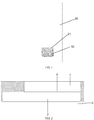
- an optical biometric identification module 10 with an optical sensing area 21 is mounted under a display screen 20.
- the optical biometric identification module 10 uses a part of the pixel units of the display screen 20 as a light source, where the pixel units which serve as the light source cover at least the optical sensing area 21.
- the pixel units which serve as the light source emit the lights to illuminate the organism.
- the organism receives the lights emitted from the light source before reflection thereof by which the lights reflected by the organism are generated.
- the organism may be a finger. When the lights emitted by the pixel units illuminate onto the finger, both of the fingerprint minutiae and non-minutiae on the finger generate emission, resulting in corresponding reflected lights.
- the optical biometric identification module 10 includes an optical channel array panel 1, an optical chip 2, and a circuit board 3.
- the optical channel array panel 1 is configured to filter the lights reflected by an organism, for example, a finger, in order to ensure that the noises in the filtered lights are weak enough, while there is a requirement of certain light transmittance.
- the optical chip 2 is configured to generate a biometric identification signal according to the filtered lights received by the optical sensing area 21.
- the circuit board 3 is configured to transmit out the biometric identification signal.
- the biometric identification signal herein may be considered to be fingerprint image information, but is not limited thereto.
- the optical chip 2 is mounted on the circuit board 3. Specifically, it may be mounted on the circuit board 3 in a manner of soldering.
- the optical channel array panel 1 is secured on the optical chip 2, and covers at least the optical sensing area 21 thereof, where the optical channel array panel 1 may be secured on the optical chip 2 by virtue of a transparent adhesive film 4 which achieves a bonding function and is of a transparent material.
- the transparent adhesive film 4 may be made of an organic material such as silica gel, a resin, and/or the like.
- the optical channel array panel 1 belongs to an optical transmission element capable of filtering the noises in the lights reflected by the organism while transmitting the light reflected thereby, i.e., enabling the filtered lights, reflected by the organism, as received by the optical chip 2 by means of the optical sensing region 21 to be approximately perpendicular to the optical channel array panel 1.
- a biometric identification signal for example, fingerprint image information, is generated by the optical chip 2 according to the filtered lights, and transmitted into a processor of the electronic device through the circuit board 3, so as to be further processed subsequently.
- the optical channel array panel 1 and the optical chip 2 are encapsulated together, so as to form a single integrated element.
- the encapsulation manner may be a plastic encapsulation.
- the portions with slashed shadows therein indicate the materials for plastic encapsulation, but is not limited thereto.
- the optical channel array panel 1 and the optical chip 2 may also be discrete elements of which both are bonded together by virtue of the transparent adhesive film 4.
- the optical channel array panel capable of filtering the lights reflected by the organism is secured on the optical chip, so as to ensure that the lights received by the optical chip is approximately perpendicular to the optical channel array panel. That is, the optical channel array panel is used to filter the noises in the lights reflected by the organism, thereby improving the accuracy of the acquired biometric identification signal.
- the second embodiment of the present application relates to an optical biometric identification module.
- the present embodiment is an elaboration of the first embodiment, and the substantial elaboration in the present embodiment lies in that the optical channel array panel 1 includes a light absorbing layer 11, and a plurality of optical channels 12 located in the light absorbing layer 11.
- the optical channel array panel 1 includes the light absorbing layer 11, and the plurality of optical channels 12 located therein, which are formed of materials with high light transmittances, for example, but not limited to, a glass.
- the optical transmittance of the optical channel 12 is greater than 95%.
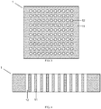
- the plurality of optical channels 12 are arranged regularly in the light absorbing layer 11 per a certain spacing. For example, the respective spacing between the plurality of optical channels 12 are kept to be equal so as to achieve a uniform arrangement, but are not limited thereto.
- the respective optical channels 12 are perpendicularly disposed on a contact surface between the optical chip 2 and the optical channel array panel 1, which corresponds to an arrangement in which there is disposed in the optical channel array panel 1 a plurality of light transmitting channels of which each is perpendicular to the contact surface between the optical chip 2 and the optical channel array panel 1, so that the lights that are perpendicularly incident into the optical channel array panel 1 can travel therethrough.
- a sidewall of each of the optical channels 12 is cladded by the light absorbing layer 11.
- the light absorbing layer 11 is composed of a light-absorbing material.
- the light absorbing material is filled between the respective optical channels 12 to form a monolithic structure, that is, the respective optical channels 12 and the light absorbing layer 11 form an integrated structure.
- the light absorbing material may be a black glass or other materials having high absorption and low light transmittance with respect to light.
- the optical transmittance of the light absorbing layer is less than or equal to 5%.
- a shape of the optical channel 12 in FIG. 3 is a circle, but not limited thereto, and the optical channel 12 may also be in other shapes, such as a square, a rectangle, a triangle, or the like, but the present embodiment is not intended to be any limitation thereon.
- a resolution of the optical channel array panel 1 is greater than or equal to 10 line pairs per millimeter.
- line pairs per millimeter which is a unit of resolution refers to the number of line pairs within one millimeter that can be discerned by an instrument. Usually, the more line pairs the instrument can discern, the higher the resolution of the instrument is.
- FIG. 5 which is a partial diagram of the optical channel array panel 1, a ratio of a diameter D of each of the optical channels 12 to a thickness T of the optical channel array panel 1 is in a range between 1:5 and 1:20.
- the ratio of the diameter D of each of the optical channels 12 to the thickness T of the optical channel array panel 1 is 1:10.
- this embodiment is not intended to be any limitation thereon, and such ratio may be set according to practical usage and effect.
- the arrangement of the optical channels 12 in the optical channel array panel 1 is only schematically depicted in FIG. 4 .
- the present embodiment is not intended to be any limitation thereon, and the arrangement may be set according to the design requirements of the optical biometric identification module 10.
- the optical channels 12 are perpendicularly disposed on the contact surface between the optical chip 2 and the optical channel array panel 1.
- the pixel units which serve as the light source, in the display screen 20 emit lights to illuminate the organism (a finger is taken as an example)
- the fingerprint minutiae and non-minutiae will both generate reflections.
- most of the lights reflected by the respective fingerprint minutiae are perpendicularly incident into the optical channel array panel 1, but there is also a minority of the lights that will be scattered outwardly during the transmission process, resulting in an oblique incidence into the optical channel array panel 1.
- the lights reflected by the fingerprint non-minutiae are also obliquely incident into the optical channel array panel 1.
- fingerprint minutia which refers to the lights approximately perpendicular with respect to the optical channel array panel 1 herein, are mixed with the lights scattered from other fingerprint minutia and the lights reflected by the fingerprint non-minutiae, i.e., the lights with oblique angles relative to the optical channel array panel 1.
- the optical channel 12 allows only the lights that is approximately perpendicularly incident into the optical channel array panel 1 from among the lights reflected by this fingerprint minutia to travel therethrough, whereas the lights with oblique angles relative to the optical channel array panel 1 mixed in the lights reflected by this fingerprint minutia are absorbed (the lights with oblique angles will be projected onto the sidewalls of the optical channels 12 so as to be absorbed by the light absorbing layer), since the optical channel 12 is perpendicular with respect to the optical chip 2 and the external portion thereof is cladded with the light absorbing layer 11. That is, the optical chip 2 can receive only the lights approximately perpendicular to the optical channel array panel 1.
- the optical channel array panel 1 can withstand a high temperature of 260° C, will not undergo deformation or discoloration thereat, and its optical performance is not affected at all.
- the third embodiment of the present application relates to an optical biometric identification module.
- the present embodiment is a elaboration of the first embodiment, and the substantial elaboration in the present embodiment lies in that the optical chip 2 includes a substrate 22 and a sensor wafer 23.
- the sensor wafer 23 is secured on the substrate 22, and a specific securing manner may be such that it is secured on the substrate 22 by virtue of the transparent adhesive film 4.
- the substrate 22 is mounted on the circuit board 3, and specifically, may be mounted on the circuit board 3 in a manner of soldering.
- the sensor wafer 23 is secured to the optical channel array panel 1 by virtue of another transparent adhesive film 5. Referring to FIGS. 1 and 6 , an optical sensing area 21 is formed on the contact surface between the sensor wafer 23 and the optical channel array panel 1.
- the sensor wafer 23 is connected to the substrate 22 through a gold wire 6, and is electrically connected to the circuit board 3 through the substrate 22.
- the optical sensing area 21 of the sensor wafer 23 receives the lights, reflected by the organism, as filtered by the optical channel array panel 1, and generates a biometric identification signal according to those lights.
- Such biometric identification signal is transmitted to the substrate 22 through the gold wire 6, and transmitted to the circuit board 3 through the substrate 22 (the circuit board 3 is connected to a processor of the electronic device, and that biometric identification signal is transmitted to the processor of the electronic device through the circuit board 3).
- the optical chip 2 further includes a solder mask 24 which is coated on the substrate 22 and faces the transparent adhesive film 4.
- the solder mask 24 can protect the circuits on the substrate 22 and prevent them from oxidation.
- the present embodiment in comparison with the first embodiment, there is provided the physical structure of the optical chip. It is to be noted that, the present embodiment may also serve as an elaboration of the second embodiment, and achieve the same technical effect.
- the fourth embodiment of the present application relates to a display apparatus applied to an electronic device, such as a mobile phone, a tablet computer, and the like.
- the display apparatus includes a display screen 20 and the optical biometric identification module 10 in any one of the first to third embodiments.
- the optical biometric identification module 10 is secured to the display screen 20.
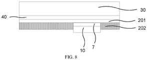
- the display screen 20 includes a self-luminescent layer 201 and an opaque layer 202.
- An aperture is disposed on the opaque layer 202.
- the optical biometric identification module 10 is secured in the aperture of the opaque layer 202 of the display screen 20, and is secured to the self-luminescent layer 201 of the display screen 20 by virtue of one transparent adhesive film 7 or other adhesive materials with high transmittances.
- the optical biometric identification module 10 may use at least part of the pixel units of the display screen 20 as a light source, that is, the optical biometric identification module 10 uses at least part of the pixel units of the self-luminescent layer 201 of the display screen 20 as a light source, and an area of the pixel units in the self-luminescent layer 201 used by the optical biometric identification module 10 covers at least the optical sensing area 21.
- a size of the aperture of the opaque layer 202 is set according to a dimension of the optical biometric identification module 10 and layout requirements of the entire apparatus, and this embodiment is not intended to be any limitations thereon, but it is necessarily guaranteed that the optical biometric module 10 can receive the lights reflected by the organism.
- the display apparatus further includes a panel 30 mainly made of a photic material such as a glass, which can ornament the appearance while protecting the display screen 20 and functioning as a support surface of the display screen 20.
- a panel 30 mainly made of a photic material such as a glass, which can ornament the appearance while protecting the display screen 20 and functioning as a support surface of the display screen 20.
- the display apparatus further includes a touch sensor 40 which mounted on or integrated in the display screen 20 (in figures, the touch sensor 40 is mounted between the self-luminescent layer 201 of the display screen 20 and the panel 30, but not limited thereto, and may also be integrated in the self-luminescent layer 201 of the display screen 20) and covers at least the optical sensing area 21.
- a touch sensor 40 which mounted on or integrated in the display screen 20 (in figures, the touch sensor 40 is mounted between the self-luminescent layer 201 of the display screen 20 and the panel 30, but not limited thereto, and may also be integrated in the self-luminescent layer 201 of the display screen 20) and covers at least the optical sensing area 21.
- the touch sensor 40 is configured to inform the processor to activate the optical biometric identification module 10 when there is detected a touch by an organism on an area of the display screen 20 above the optical sensing area 21, so that the optical biometric module 10 is activated to complete the biometric identification only upon receiving the touch by the organism when the electronic device is in a screen-off state.
- the display screen 20 may be controlled to display one dark prompting picture (a picture that is dark but visible to the naked eye) at an area corresponding to the optical sensing area 21, so as to facilitate an accurate positioning of the optical sensing area 21 by the user.
- the optical channel array panel capable of filtering the lights reflected by the organism is secured on the optical chip, so as to ensure that the lights received by the optical chip are approximately perpendicular to the optical channel array panel. That is, the optical channel array panel is used to filter the noises in the lights reflected by the organism, thereby improving the accuracy of the acquired biometric identification signal. Meanwhile, the processor is informed to activate the optical biometric identification module only when the touch by the organism is received, so the power consumption is reduced.
- the fifth embodiment of the present application relates to an electronic device, such as a mobile phone, a tablet computer, and the like.
- the electronic device includes the display apparatus in the fourth embodiment.
- the optical channel array panel capable of filtering the lights reflected by the organism is secured on the optical chip, so as to ensure that the lights received by the optical chip are approximately perpendicular to the optical channel array panel. That is, the optical channel array panel is used to filter the noises in the lights reflected by the organism, thereby improving the accuracy of the acquired biometric identification signal.
Landscapes
- Engineering & Computer Science (AREA)
- Physics & Mathematics (AREA)
- General Physics & Mathematics (AREA)
- Multimedia (AREA)
- Theoretical Computer Science (AREA)
- Human Computer Interaction (AREA)
- Optics & Photonics (AREA)
- Measurement Of The Respiration, Hearing Ability, Form, And Blood Characteristics Of Living Organisms (AREA)
- Image Input (AREA)
Abstract
Description
- The present application relates to the field of biometric identification technology, and more particularly, to an optical biometric identification module, a display apparatus, and an electronic device.
- With the rapid development of biometric identification technology, the biometric identification technology of which the representative one is fingerprint identification has been widely adapted in various electronic devices, such as a mobile phone, a tablet computer, or the like. At present, the biometric identification technology adopted by most of the electronic devices available commercially is a capacitive fingerprint identification with a limited penetration thickness, influence from humidity of the fingers, and a requirement of a front-boring or thinning on the electronic device by which a better identification effect is ensured. Meanwhile, a fingerprint identification apparatus is generally placed centrally for the purpose of a better effect of the appearance. Therefore, increase in a screen-to-body ratio of the electronic device is limited when the fingerprint identification apparatus is placed in the front thereof.
- At present, in order to increase the screen-to-body ratio, the electronic device may employ an optical fingerprint identification apparatus integrated under the screen thereof. However, the inventor has found there is also a problem that the optical fingerprint identification apparatus acquires the fingerprint image information by collecting the lights reflected by the finger and performing an identification on the collected reflected lights, wherein the fingerprint image information is acquired primarily by identifying respective minutiae of the fingerprint (ridges and valleys of the fingerprint). However, the lights reflected by the respective minutiae of the fingerprint may probably interfere therewith mutually, and the lights reflected by the fingerprint non-minutiae may also interfere with those reflected by the respective minutiae. Such interference with the lights reflected by the respective minutiae is the noise therein. Since the lights reflected by the respective minutiae contain noises, this will result in an error in the identification of the respective fingerprint minutiae, i.e., this will result in influence on the effect of the fingerprint identification.
- The objective of some embodiments of the present application is to provide an optical biometric identification module, a display apparatus, and an electronic device, which filters the noises in the lights reflected by an organism by using an optical channel array panel, thereby improving an accuracy of an acquired biometric identification signal.
- In an embodiment of the present application, there is provided an optical biometric identification module, including an optical channel array panel configured to filter the lights reflected by an organism; an optical chip configured to generate a biometric identification signal according to the filtered lights received by an optical sensing area; and a circuit board configured to transmit out the biometric identification signal, the optical chip being mounted on the circuit board, and the optical channel array panel being secured on the optical chip and covering at least the optical sensing area of the optical chip.
- In an embodiment of the present application, there is further provided a display apparatus, including a display screen; and the optical biometric identification module as described above, the optical biometric identification module being secured to the display screen, and an optical fingerprint identification module using at least part of pixel units of the display screen as a light source.
- In an embodiment of the present application, there is further provided an electronic device including the display apparatus as described above.
- In the present application in comparison with the prior art, the optical channel array panel capable of filtering the lights reflected by the organism is secured on the optical chip, so as to ensure that the lights received by the optical chip are approximately perpendicular to the optical channel array panel. That is, the optical channel array panel is used to filter the noises in the lights reflected by the organism, thereby improving the accuracy of the acquired biometric identification signal.
- In addition, the optical channel array panel includes a light absorbing layer; and a plurality of optical channels located in the light absorbing layer, each of said optical channels being perpendicularly disposed on a contact surface between the optical chip and the optical channel array panel, and a sidewall thereof being cladding by the light absorbing layer. In the present embodiment, there is provided a physical structure of the optical channel array panel, so as to meet the requirements on practical design.
- In addition, a ratio of a diameter of each of the optical channels to a thickness of the optical channel array panel is in a range between 1:5 and 1:20, and a resolution of the channel array panel is greater than or equal to 10 line pairs per millimeter. In the present embodiment, there is provided the specific ranges of the resolution of the optical channel array panel and of the ratio of the diameter of the optical channel to the thickness of the optical channel array panel.
- In addition, the ratio of the diameter of each of the optical channels to the thickness of the optical channel array panel is 1:10. In the present embodiment, there is provided a preferred ratio of the diameter of the optical channel to the thickness of the optical channel array panel, thereby improving further the accuracy of the acquired biometric signal.
- In addition, an optical transmittance of each optical channel is greater than 95%.
- In addition, an optical transmittance of the light absorbing layer is less than or equal to 5%.
- In addition, the optical channel array panel and the optical chip are encapsulated together. In the present embodiment, the optical channel array panel and the optical chip are encapsulated together, so as to facilitate the practical applications.
- In addition, the optical chip includes a substrate; and a sensor wafer secured on the substrate, the substrate being mounted on the circuit board, and the sensor wafer being electrically connected to the circuit board through the substrate. In the present embodiment, there is provided a physical structure of the optical chip.
- In addition, the optical biometric identification module is an optical fingerprint identification module.
- One or more embodiments are illustrated exemplarily by the diagrams in the accompanying drawings corresponding thereto, and those exemplary illustrations are not intended to limit the embodiments. The elements with the same reference numerals in the drawings indicate the like elements, unless specifically stated otherwise. The diagrams in the accompany drawings is not intended to be the limitation on scale.
-
FIG. 1 is a schematic diagram of structure of an electronic device according to a first embodiment of the present application; -
FIG. 2 is a schematic diagram of structure of a biometric identification module according to the first embodiment of the present application; -
FIG. 3 is a top view of an optical channel array panel according to a second embodiment of the present application; -
FIG. 4 is a cross-sectional view of the optical channel array panel according to the second embodiment of the present application; -
FIG. 5 is a partial schematic diagram of the optical channel array panel according to the second embodiment of the present application; -
FIG. 6 is a schematic diagram of structure of a biometric identification module according to a third embodiment of the present application; -
FIG. 7 is a schematic diagram of structure of a display apparatus according to a fourth embodiment of the present application; and -
FIG. 8 is a schematic diagram of structure of a display apparatus including a touch sensor according to the fourth embodiment of the present application. - For further clarifying the objectives, technical solutions, and advantages of the present application, some embodiments thereof will be further described in detail below in conjunction with the accompanying drawings and the embodiments. It should be understood that the specific embodiments described herein are merely used to explain the present application, rather than the limitation thereon.
- The first embodiment of the present application relates to an optical biometric identification module applied to an electronic device, such as a mobile terminal device, e.g., a mobile phone, or a tablet computer, and other types of electronic devices, such as a card punch. The optical biometric identification module may be an optical fingerprint identification module. When it is applied to an electronic device without a display screen, a light source is required to be configured additionally. When it is applied to an electronic device with a display screen, it may be integrated thereunder, which facilitates an improvement of a screen-to-body ratio of the electronic device. Moreover, at least part of pixel units of the display screen can be used as the light source, without any requirement of the additionally configured light source.
- More specifically, the display screen of the electronic device may be a Liquid Crystal Display (LCD) screen, an Organic Light Emitting Diode (OLED) display screen, a micro-Light Emitting Diode (micro-LED) display screen, or other types of flat panel display screen. When the electronic device is applied to a smart mobile terminal device, a touch display screen may be selected as the display screen in order to have functions of both a touch control and a displaying. For example, a touch sensor may be mounted on or integrated into the display screen. The optical fingerprint identification module may be integrated into the display screen by means of a structure of an Under display or an In display. For example, the optical fingerprint identification module for which a single discrete functional module may be utilized may be directly disposed under the display area of the display screen, such that it can integrate and reuse some of the functions of the display screen (such as a utilization of the self-luminescent display pixels of the display screen as the light source, etc.).
- In this embodiment, an illustration is made by taking an example where the optical biometric identification module which is the optical fingerprint identification module is applied to the electronic device with the display screen. Referring to
FIG. 1 , an opticalbiometric identification module 10 with anoptical sensing area 21 is mounted under adisplay screen 20. The opticalbiometric identification module 10 uses a part of the pixel units of thedisplay screen 20 as a light source, where the pixel units which serve as the light source cover at least theoptical sensing area 21. When there is a touch by an organism on the area of thedisplay screen 20 above theoptical sensing area 21, the pixel units which serve as the light source emit the lights to illuminate the organism. The organism receives the lights emitted from the light source before reflection thereof by which the lights reflected by the organism are generated. In the present embodiment, the organism may be a finger. When the lights emitted by the pixel units illuminate onto the finger, both of the fingerprint minutiae and non-minutiae on the finger generate emission, resulting in corresponding reflected lights. - Referring to
FIG. 2 , in the present embodiment, the opticalbiometric identification module 10 includes an opticalchannel array panel 1, anoptical chip 2, and acircuit board 3. - The optical
channel array panel 1 is configured to filter the lights reflected by an organism, for example, a finger, in order to ensure that the noises in the filtered lights are weak enough, while there is a requirement of certain light transmittance. Theoptical chip 2 is configured to generate a biometric identification signal according to the filtered lights received by theoptical sensing area 21. Thecircuit board 3 is configured to transmit out the biometric identification signal. In the present embodiment, the biometric identification signal herein may be considered to be fingerprint image information, but is not limited thereto. - Referring to
FIG. 2 , theoptical chip 2 is mounted on thecircuit board 3. Specifically, it may be mounted on thecircuit board 3 in a manner of soldering. The opticalchannel array panel 1 is secured on theoptical chip 2, and covers at least theoptical sensing area 21 thereof, where the opticalchannel array panel 1 may be secured on theoptical chip 2 by virtue of a transparentadhesive film 4 which achieves a bonding function and is of a transparent material. The higher the light transmittance of the transparentadhesive film 4 is, the less the influence on the lights is. The transparentadhesive film 4 may be made of an organic material such as silica gel, a resin, and/or the like. - The optical
channel array panel 1 belongs to an optical transmission element capable of filtering the noises in the lights reflected by the organism while transmitting the light reflected thereby, i.e., enabling the filtered lights, reflected by the organism, as received by theoptical chip 2 by means of theoptical sensing region 21 to be approximately perpendicular to the opticalchannel array panel 1. A biometric identification signal, for example, fingerprint image information, is generated by theoptical chip 2 according to the filtered lights, and transmitted into a processor of the electronic device through thecircuit board 3, so as to be further processed subsequently. - In the present embodiment herein, the optical
channel array panel 1 and theoptical chip 2 are encapsulated together, so as to form a single integrated element. The encapsulation manner may be a plastic encapsulation. Referring toFIG. 2 , the portions with slashed shadows therein indicate the materials for plastic encapsulation, but is not limited thereto. The opticalchannel array panel 1 and theoptical chip 2 may also be discrete elements of which both are bonded together by virtue of the transparentadhesive film 4. - In the present embodiment in comparison with the prior art, the optical channel array panel capable of filtering the lights reflected by the organism is secured on the optical chip, so as to ensure that the lights received by the optical chip is approximately perpendicular to the optical channel array panel. That is, the optical channel array panel is used to filter the noises in the lights reflected by the organism, thereby improving the accuracy of the acquired biometric identification signal.
- The second embodiment of the present application relates to an optical biometric identification module. The present embodiment is an elaboration of the first embodiment, and the substantial elaboration in the present embodiment lies in that the optical
channel array panel 1 includes alight absorbing layer 11, and a plurality ofoptical channels 12 located in thelight absorbing layer 11. - In the present embodiment, referring to
FIGS. 3 and 4 which are the top view and the cross-sectional view of the opticalchannel array panel 1 respectively, the opticalchannel array panel 1 includes thelight absorbing layer 11, and the plurality ofoptical channels 12 located therein, which are formed of materials with high light transmittances, for example, but not limited to, a glass. Preferably, the optical transmittance of theoptical channel 12 is greater than 95%. The plurality ofoptical channels 12 are arranged regularly in thelight absorbing layer 11 per a certain spacing. For example, the respective spacing between the plurality ofoptical channels 12 are kept to be equal so as to achieve a uniform arrangement, but are not limited thereto. In addition, the respectiveoptical channels 12 are perpendicularly disposed on a contact surface between theoptical chip 2 and the opticalchannel array panel 1, which corresponds to an arrangement in which there is disposed in the optical channel array panel 1 a plurality of light transmitting channels of which each is perpendicular to the contact surface between theoptical chip 2 and the opticalchannel array panel 1, so that the lights that are perpendicularly incident into the opticalchannel array panel 1 can travel therethrough. Herein, a sidewall of each of theoptical channels 12 is cladded by thelight absorbing layer 11. - In the present embodiment, the
light absorbing layer 11 is composed of a light-absorbing material. As can be seen fromFIG. 3 , the light absorbing material is filled between the respectiveoptical channels 12 to form a monolithic structure, that is, the respectiveoptical channels 12 and thelight absorbing layer 11 form an integrated structure. Such an implementation is not intended to be any limitation on the manner in which thelight absorbing layer 11 and the respectiveoptical channels 12 are combined, as long as thelight absorbing layer 11 is able to clad the sidewalls of the respectiveoptical channels 12 to absorb the noises. Herein, the light absorbing material may be a black glass or other materials having high absorption and low light transmittance with respect to light. Preferably, the optical transmittance of the light absorbing layer is less than or equal to 5%. - It is to be noted that a shape of the
optical channel 12 inFIG. 3 (a top view of the optical channel array panel 1) is a circle, but not limited thereto, and theoptical channel 12 may also be in other shapes, such as a square, a rectangle, a triangle, or the like, but the present embodiment is not intended to be any limitation thereon. - Referring to
FIG. 4 , a resolution of the opticalchannel array panel 1 is greater than or equal to 10 line pairs per millimeter. Herein, the term line pairs per millimeter which is a unit of resolution refers to the number of line pairs within one millimeter that can be discerned by an instrument. Usually, the more line pairs the instrument can discern, the higher the resolution of the instrument is. Referring toFIG. 5 , which is a partial diagram of the opticalchannel array panel 1, a ratio of a diameter D of each of theoptical channels 12 to a thickness T of the opticalchannel array panel 1 is in a range between 1:5 and 1:20. - Preferably, the ratio of the diameter D of each of the
optical channels 12 to the thickness T of the opticalchannel array panel 1 is 1:10. However, this embodiment is not intended to be any limitation thereon, and such ratio may be set according to practical usage and effect. - It is to be noted that the arrangement of the
optical channels 12 in the opticalchannel array panel 1 is only schematically depicted inFIG. 4 . However, the present embodiment is not intended to be any limitation thereon, and the arrangement may be set according to the design requirements of the opticalbiometric identification module 10. - In the present embodiment, the
optical channels 12 are perpendicularly disposed on the contact surface between theoptical chip 2 and the opticalchannel array panel 1. When the pixel units, which serve as the light source, in thedisplay screen 20 emit lights to illuminate the organism (a finger is taken as an example), the fingerprint minutiae and non-minutiae will both generate reflections. Herein, most of the lights reflected by the respective fingerprint minutiae are perpendicularly incident into the opticalchannel array panel 1, but there is also a minority of the lights that will be scattered outwardly during the transmission process, resulting in an oblique incidence into the opticalchannel array panel 1. The lights reflected by the fingerprint non-minutiae are also obliquely incident into the opticalchannel array panel 1. Herein, an illustration is made by taking one fingerprint minutia as an example. The lights reflected by this fingerprint minutia, which refers to the lights approximately perpendicular with respect to the opticalchannel array panel 1 herein, are mixed with the lights scattered from other fingerprint minutia and the lights reflected by the fingerprint non-minutiae, i.e., the lights with oblique angles relative to the opticalchannel array panel 1. When the light reflected by this fingerprint minutia travels through theoptical channel 12 in the opticalchannel array panel 1, theoptical channel 12 allows only the lights that is approximately perpendicularly incident into the opticalchannel array panel 1 from among the lights reflected by this fingerprint minutia to travel therethrough, whereas the lights with oblique angles relative to the opticalchannel array panel 1 mixed in the lights reflected by this fingerprint minutia are absorbed (the lights with oblique angles will be projected onto the sidewalls of theoptical channels 12 so as to be absorbed by the light absorbing layer), since theoptical channel 12 is perpendicular with respect to theoptical chip 2 and the external portion thereof is cladded with thelight absorbing layer 11. That is, theoptical chip 2 can receive only the lights approximately perpendicular to the opticalchannel array panel 1. - In the present embodiment, the optical
channel array panel 1 can withstand a high temperature of 260° C, will not undergo deformation or discoloration thereat, and its optical performance is not affected at all. - In the present embodiment in comparison with the first embodiment, there is provided the physical structure of the optical channel array panel to meet the practical design requirements.
- The third embodiment of the present application relates to an optical biometric identification module. The present embodiment is a elaboration of the first embodiment, and the substantial elaboration in the present embodiment lies in that the
optical chip 2 includes asubstrate 22 and asensor wafer 23. - Referring to
FIG. 6 , thesensor wafer 23 is secured on thesubstrate 22, and a specific securing manner may be such that it is secured on thesubstrate 22 by virtue of the transparentadhesive film 4. Thesubstrate 22 is mounted on thecircuit board 3, and specifically, may be mounted on thecircuit board 3 in a manner of soldering. - The
sensor wafer 23 is secured to the opticalchannel array panel 1 by virtue of another transparent adhesive film 5. Referring toFIGS. 1 and6 , anoptical sensing area 21 is formed on the contact surface between thesensor wafer 23 and the opticalchannel array panel 1. Thesensor wafer 23 is connected to thesubstrate 22 through agold wire 6, and is electrically connected to thecircuit board 3 through thesubstrate 22. Theoptical sensing area 21 of thesensor wafer 23 receives the lights, reflected by the organism, as filtered by the opticalchannel array panel 1, and generates a biometric identification signal according to those lights. Such biometric identification signal is transmitted to thesubstrate 22 through thegold wire 6, and transmitted to thecircuit board 3 through the substrate 22 (thecircuit board 3 is connected to a processor of the electronic device, and that biometric identification signal is transmitted to the processor of the electronic device through the circuit board 3). - In the present embodiment, referring to
FIG. 6 , theoptical chip 2 further includes asolder mask 24 which is coated on thesubstrate 22 and faces the transparentadhesive film 4. Thesolder mask 24 can protect the circuits on thesubstrate 22 and prevent them from oxidation. - In the present embodiment in comparison with the first embodiment, there is provided the physical structure of the optical chip. It is to be noted that, the present embodiment may also serve as an elaboration of the second embodiment, and achieve the same technical effect.
- The fourth embodiment of the present application relates to a display apparatus applied to an electronic device, such as a mobile phone, a tablet computer, and the like. The display apparatus includes a
display screen 20 and the opticalbiometric identification module 10 in any one of the first to third embodiments. - Referring to
FIGS. 1 and7 , the opticalbiometric identification module 10 is secured to thedisplay screen 20. Specifically, thedisplay screen 20 includes a self-luminescent layer 201 and anopaque layer 202. An aperture is disposed on theopaque layer 202. The opticalbiometric identification module 10 is secured in the aperture of theopaque layer 202 of thedisplay screen 20, and is secured to the self-luminescent layer 201 of thedisplay screen 20 by virtue of onetransparent adhesive film 7 or other adhesive materials with high transmittances. Moreover, at the time of securing, it is required that the cleanness in the aperture of theopaque layer 202 is guaranteed, and there are no substance such as foreign matter, dirt, dust, or the like that may affect the light transmission, so as to prevent the opticalbiometric identification module 10 from being affected by the foreign matter when receiving the light reflected by the organism. The opticalbiometric identification module 10 may use at least part of the pixel units of thedisplay screen 20 as a light source, that is, the opticalbiometric identification module 10 uses at least part of the pixel units of the self-luminescent layer 201 of thedisplay screen 20 as a light source, and an area of the pixel units in the self-luminescent layer 201 used by the opticalbiometric identification module 10 covers at least theoptical sensing area 21. - In the present embodiment, a size of the aperture of the
opaque layer 202 is set according to a dimension of the opticalbiometric identification module 10 and layout requirements of the entire apparatus, and this embodiment is not intended to be any limitations thereon, but it is necessarily guaranteed that the opticalbiometric module 10 can receive the lights reflected by the organism. - The display apparatus further includes a
panel 30 mainly made of a photic material such as a glass, which can ornament the appearance while protecting thedisplay screen 20 and functioning as a support surface of thedisplay screen 20. - Preferably, referring to
FIGS. 1 and8 , the display apparatus further includes atouch sensor 40 which mounted on or integrated in the display screen 20 (in figures, thetouch sensor 40 is mounted between the self-luminescent layer 201 of thedisplay screen 20 and thepanel 30, but not limited thereto, and may also be integrated in the self-luminescent layer 201 of the display screen 20) and covers at least theoptical sensing area 21. - The
touch sensor 40 is configured to inform the processor to activate the opticalbiometric identification module 10 when there is detected a touch by an organism on an area of thedisplay screen 20 above theoptical sensing area 21, so that the opticalbiometric module 10 is activated to complete the biometric identification only upon receiving the touch by the organism when the electronic device is in a screen-off state. Preferably, thedisplay screen 20 may be controlled to display one dark prompting picture (a picture that is dark but visible to the naked eye) at an area corresponding to theoptical sensing area 21, so as to facilitate an accurate positioning of theoptical sensing area 21 by the user. - In the present embodiment in comparison with the prior art, the optical channel array panel capable of filtering the lights reflected by the organism is secured on the optical chip, so as to ensure that the lights received by the optical chip are approximately perpendicular to the optical channel array panel. That is, the optical channel array panel is used to filter the noises in the lights reflected by the organism, thereby improving the accuracy of the acquired biometric identification signal. Meanwhile, the processor is informed to activate the optical biometric identification module only when the touch by the organism is received, so the power consumption is reduced.
- The fifth embodiment of the present application relates to an electronic device, such as a mobile phone, a tablet computer, and the like. The electronic device includes the display apparatus in the fourth embodiment.
- In the present embodiment in comparison with the prior art, the optical channel array panel capable of filtering the lights reflected by the organism is secured on the optical chip, so as to ensure that the lights received by the optical chip are approximately perpendicular to the optical channel array panel. That is, the optical channel array panel is used to filter the noises in the lights reflected by the organism, thereby improving the accuracy of the acquired biometric identification signal.
- As will be understood by a person of ordinary skill in the art, the above various embodiments are specific embodiments for implementing the present application, and various changes in form and detail can be made without departing from the spirit and scope of the present application in practical applications.
Claims (13)
- An optical biometric identification module, characterized by comprisingan optical channel array panel configured to filter lights reflected by an organism;an optical chip configured to generate a biometric identification signal according to the filtered lights received by an optical sensing area; anda circuit board configured to transmit out the biometric identification signal;the optical chip being mounted on the circuit board, and the optical channel array panel being secured on the optical chip and covering at least the optical sensing area of the optical chip.
- The optical biometric identification module according to claim 1, characterized in that, the optical channel array panel comprises a light absorbing layer and a plurality of optical channels located in the light absorbing layer;
each of said optical channels being perpendicularly disposed on a contact surface between the optical chip and the optical channel array panel, and a sidewall thereof being cladded by the light absorbing layer. - The optical biometric identification module according to claim 2, characterized in that, a ratio of a diameter of each of said optical channels to a thickness of the optical channel array panel is in a range between 1:5 and 1:20, and a resolution of the channel array panel is greater than or equal to 10 line pairs per millimeter.
- The optical biometric identification module according to claim 3, characterized in that, the ratio of the diameter of each of said optical channels to the thickness of the optical channel array panel is 1:10.
- The optical biometric identification module according to claim 2, characterized in that, an optical transmittance of each of said optical channels is greater than 95%.
- The optical biometric identification module according to claim 2, characterized in that, an optical transmittance of the light absorbing layer is less than or equal to 5%.
- The optical biometric identification module according to claim 1, characterized in that, the optical channel array panel and the optical chip are encapsulated together.
- The optical biometric identification module according to any one of claims 1 to 7, characterized in that, the optical chip comprises a substrate and a sensor wafer secured on the substrate;
the substrate is mounted on the circuit board;
the sensor wafer is electrically connected to the circuit board through the substrate. - The optical biometric identification module according to any one of claims 1 to 8, characterized in that, the optical biometric identification module is an optical fingerprint identification module.
- A display apparatus, characterized by comprising
a display screen and
the optical biometric identification module according to any one of claims 1 to 9;
the optical biometric identification module being secured to the display screen, and the optical biometric identification module uses at least part of pixel units of the display screen as a light source. - The display apparatus according to claim 10, characterized in that, the optical biometric identification module is secured in an aperture of an opaque layer of the display screen.
- The display apparatus according to claim 11, characterized in that, the display apparatus further comprises a touch sensor configured to inform a processor to activate the optical biometric identification module when there is detected a touch by an organism on the optical sensing area, the touch sensor being mounted on or integrated in the display screen, and the touch sensor covering at least the optical sensing area.
- An electronic device, characterized by comprising the display apparatus according to any one of claims 10 to 12.
Applications Claiming Priority (1)
| Application Number | Priority Date | Filing Date | Title |
|---|---|---|---|
| PCT/CN2017/088165 WO2018227399A1 (en) | 2017-06-13 | 2017-06-13 | Optical biological recognition module, display device, and electronic equipment |
Publications (2)
| Publication Number | Publication Date |
|---|---|
| EP3444747A1 true EP3444747A1 (en) | 2019-02-20 |
| EP3444747A4 EP3444747A4 (en) | 2019-08-14 |
Family
ID=63801057
Family Applications (1)
| Application Number | Title | Priority Date | Filing Date |
|---|---|---|---|
| EP17905904.3A Withdrawn EP3444747A4 (en) | 2017-06-13 | 2017-06-13 | OPTICAL BIOLOGICAL RECOGNITION MODULE, DISPLAY DEVICE AND ELECTRONIC EQUIPMENT |
Country Status (4)
| Country | Link |
|---|---|
| US (1) | US10733411B2 (en) |
| EP (1) | EP3444747A4 (en) |
| CN (1) | CN108684207A (en) |
| WO (1) | WO2018227399A1 (en) |
Cited By (1)
| Publication number | Priority date | Publication date | Assignee | Title |
|---|---|---|---|---|
| EP3696716A4 (en) * | 2018-12-29 | 2020-10-21 | Shenzhen Goodix Technology Co., Ltd. | FINGERPRINT IDENTIFICATION DEVICE AND ELECTRONIC DEVICE |
Families Citing this family (5)
| Publication number | Priority date | Publication date | Assignee | Title |
|---|---|---|---|---|
| CN108922469B (en) * | 2018-06-29 | 2021-04-02 | 武汉天马微电子有限公司 | A display panel and display device |
| CN113343829B (en) * | 2019-05-29 | 2024-04-09 | 深圳市汇顶科技股份有限公司 | Fingerprint recognition device and electronic device |
| CN111666926A (en) * | 2020-07-06 | 2020-09-15 | 武汉华星光电技术有限公司 | Display panel |
| CN111985431B (en) * | 2020-08-27 | 2024-08-13 | 深圳市汇顶科技股份有限公司 | Fingerprint identification device and electronic equipment |
| CN113449685A (en) * | 2021-07-16 | 2021-09-28 | 维沃移动通信有限公司 | Optical fingerprint identification device, optical fingerprint identification method and electronic equipment |
Family Cites Families (36)
| Publication number | Priority date | Publication date | Assignee | Title |
|---|---|---|---|---|
| JPH0636593A (en) | 1992-07-14 | 1994-02-10 | Mitsubishi Electric Corp | Semiconductor memory device |
| JP2002117393A (en) | 2000-10-05 | 2002-04-19 | Omron Corp | Fingerprint recognition sensor |
| US7519486B2 (en) | 2006-03-31 | 2009-04-14 | Atmel Corporation | Method and apparatus to test the power-on-reset trip point of an integrated circuit |
| CN101419522B (en) | 2008-11-28 | 2010-12-15 | 深圳市汇顶科技有限公司 | Capacitance touch detection device and detection method thereof |
| US20100207890A1 (en) | 2009-02-19 | 2010-08-19 | Ideacom Technology Corporation (Taiwan) | Singal detecting apparatus |
| CN101571919B (en) * | 2009-05-26 | 2011-08-31 | 重庆大学 | Face recognition method based on optics nonsubsampled Contourlet conversion |
| CN102004339B (en) * | 2009-09-02 | 2012-05-30 | 北京京东方光电科技有限公司 | Substrate and manufacturing method thereof, liquid crystal panel and manufacturing method thereof |
| CN101753212B (en) | 2009-12-30 | 2012-11-21 | 武汉电信器件有限公司 | Detecting device and detecting method of time sequence parameters of small package pluggable transceiver |
| CN101799734B (en) | 2010-03-29 | 2012-05-09 | 深圳龙多电子科技有限公司 | Key detection method for capacitive touch screen |
| US9342729B2 (en) * | 2010-08-06 | 2016-05-17 | Secugen Corporation | Fake fingerprint detection system |
| CN102111136B (en) | 2011-01-28 | 2013-05-15 | 钜泉光电科技(上海)股份有限公司 | Chip power-on reset circuit |
| KR20130056082A (en) * | 2011-11-21 | 2013-05-29 | 삼성전기주식회사 | Fingerprint sensor and operating method thereof |
| CN102968217B (en) | 2012-12-07 | 2016-01-20 | 深圳市汇顶科技股份有限公司 | The datum renewal method of touch-screen, system and touch control terminal |
| CN203537424U (en) | 2013-08-23 | 2014-04-09 | 深圳欧菲光科技股份有限公司 | Touch panel, touch display screen and cell phone thereof |
| CN103458073B (en) | 2013-08-23 | 2015-12-23 | 深圳欧菲光科技股份有限公司 | Contact panel, touching display screen and mobile phone thereof |
| US9864507B2 (en) | 2013-09-26 | 2018-01-09 | Synaptics Incorporated | Methods and apparatus for click detection on a force pad using dynamic thresholds |
| KR101869624B1 (en) * | 2013-11-22 | 2018-06-21 | 선전 구딕스 테크놀로지 컴퍼니, 리미티드 | Secure human fingerprint sensor |
| US10043847B2 (en) * | 2014-08-26 | 2018-08-07 | Gingy Technology Inc. | Image capturing module and electrical apparatus |
| CN106233306B (en) * | 2014-09-06 | 2019-09-27 | 深圳市汇顶科技股份有限公司 | Method for registering and identifying fingerprint profile on mobile device and mobile device |
| US10732771B2 (en) * | 2014-11-12 | 2020-08-04 | Shenzhen GOODIX Technology Co., Ltd. | Fingerprint sensors having in-pixel optical sensors |
| CN105676105A (en) | 2014-11-19 | 2016-06-15 | 比亚迪股份有限公司 | Chip test method and chip test machine |
| CN104463107A (en) | 2014-11-21 | 2015-03-25 | 上海箩箕技术有限公司 | Backlight plate, optical imaging device and identification equipment |
| KR102290892B1 (en) * | 2014-12-12 | 2021-08-19 | 엘지전자 주식회사 | Mobile terminal and method for controlling the same |
| CN105989325A (en) * | 2015-01-29 | 2016-10-05 | 深圳印象认知技术有限公司 | Fingerprint palm print image collector of honeycomb structure and terminal device |
| US10147757B2 (en) * | 2015-02-02 | 2018-12-04 | Synaptics Incorporated | Image sensor structures for fingerprint sensing |
| US9811711B2 (en) * | 2015-02-22 | 2017-11-07 | Microsoft Technology Licensing, Llc | Fingerprint detection with transparent cover |
| TW201640418A (en) * | 2015-05-04 | 2016-11-16 | 曦威科技股份有限公司 | Fingerprint detecting device, mobile device using the same, and manufacturing method thereof |
| TWI547884B (en) | 2015-07-09 | 2016-09-01 | 金佶科技股份有限公司 | Fingerprint identification module |
| US9934418B2 (en) * | 2015-12-03 | 2018-04-03 | Synaptics Incorporated | Display integrated optical fingerprint sensor with angle limiting reflector |
| CN105678233B (en) * | 2015-12-30 | 2020-05-19 | 北京眼神智能科技有限公司 | Fingerprint and finger vein based composite identification method, device and system |
| CN105550664A (en) | 2016-01-08 | 2016-05-04 | 上海箩箕技术有限公司 | Optical fingerprint sensor module |
| CN205302331U (en) * | 2016-01-14 | 2016-06-08 | 深圳市汇顶科技股份有限公司 | Biological detection device |
| CN205484701U (en) | 2016-03-14 | 2016-08-17 | 武汉梦芯科技有限公司 | Last electricity time of ICPMU and relapse powering up and down stability test circuit |
| CN106324395B (en) | 2016-08-17 | 2019-09-13 | 上海斐讯数据通信技术有限公司 | A power-on reset test method and system |
| CN206515844U (en) | 2017-02-13 | 2017-09-22 | 深圳市汇顶科技股份有限公司 | sensing device and terminal device |
| KR102354415B1 (en) * | 2017-05-12 | 2022-01-21 | 삼성전자주식회사 | Electronic Device and Control Method thereof |
-
2017
- 2017-06-13 EP EP17905904.3A patent/EP3444747A4/en not_active Withdrawn
- 2017-06-13 WO PCT/CN2017/088165 patent/WO2018227399A1/en not_active Ceased
- 2017-06-13 CN CN201780007263.7A patent/CN108684207A/en active Pending
-
2018
- 2018-10-23 US US16/168,263 patent/US10733411B2/en active Active
Cited By (1)
| Publication number | Priority date | Publication date | Assignee | Title |
|---|---|---|---|---|
| EP3696716A4 (en) * | 2018-12-29 | 2020-10-21 | Shenzhen Goodix Technology Co., Ltd. | FINGERPRINT IDENTIFICATION DEVICE AND ELECTRONIC DEVICE |
Also Published As
| Publication number | Publication date |
|---|---|
| WO2018227399A1 (en) | 2018-12-20 |
| US20190057239A1 (en) | 2019-02-21 |
| CN108684207A (en) | 2018-10-19 |
| US10733411B2 (en) | 2020-08-04 |
| EP3444747A4 (en) | 2019-08-14 |
Similar Documents
| Publication | Publication Date | Title |
|---|---|---|
| US10733411B2 (en) | Optical biometric identification module, display apparatus, and electronic device | |
| CN109496313B (en) | Fingerprint identification device and electronic equipment | |
| CN110770746B (en) | Fingerprint identification device and electronic equipment | |
| CN109061946B (en) | Display components and electronic equipment | |
| CN209640879U (en) | The device and electronic equipment of fingerprint recognition | |
| US20210103714A1 (en) | Fingerprint identification apparatus and electronic device | |
| US20200097699A1 (en) | Fingerprint identification apparatus and electronic device | |
| WO2019085968A1 (en) | Fingerprint identification module, fingerprint identification method, and display apparatus | |
| CN110036396B (en) | Fingerprint identification devices and electronic equipment | |
| CN109643377A (en) | Fingerprint identification device and electronic equipment | |
| CN207037681U (en) | Optical biometric identification module, display device and electronic equipment | |
| US10482304B2 (en) | Fingerprint and palmprint image collector with honeycomb structure, and terminal device | |
| CN211554956U (en) | Fingerprint sensing module and electronic device | |
| CN208954114U (en) | Fingerprint identification devices and electronic equipment | |
| EP3731135B1 (en) | Method and device for fingerprint recognition, and terminal device | |
| CN106599768A (en) | Optical device | |
| EP3731134A1 (en) | Method and apparatus for fingerprint recognition, and terminal device | |
| CN210605736U (en) | Fingerprint detection device, display screen and electronic equipment | |
| CN110598663A (en) | Display screen assembly, electronic equipment and fingerprint processing method | |
| CN211087274U (en) | Fingerprint detection device and electronic equipment | |
| CN107798273B (en) | Method for improving optical fingerprint identification performance | |
| CN210295111U (en) | Fingerprint identification device and electronic equipment | |
| CN214751918U (en) | Image capturing device | |
| CN210864764U (en) | Fingerprint identification device and electronic equipment | |
| CN114529955A (en) | Image capturing device |
Legal Events
| Date | Code | Title | Description |
|---|---|---|---|
| STAA | Information on the status of an ep patent application or granted ep patent |
Free format text: STATUS: UNKNOWN |
|
| STAA | Information on the status of an ep patent application or granted ep patent |
Free format text: STATUS: THE INTERNATIONAL PUBLICATION HAS BEEN MADE |
|
| PUAI | Public reference made under article 153(3) epc to a published international application that has entered the european phase |
Free format text: ORIGINAL CODE: 0009012 |
|
| STAA | Information on the status of an ep patent application or granted ep patent |
Free format text: STATUS: REQUEST FOR EXAMINATION WAS MADE |
|
| 17P | Request for examination filed |
Effective date: 20181023 |
|
| AK | Designated contracting states |
Kind code of ref document: A1 Designated state(s): AL AT BE BG CH CY CZ DE DK EE ES FI FR GB GR HR HU IE IS IT LI LT LU LV MC MK MT NL NO PL PT RO RS SE SI SK SM TR |
|
| AX | Request for extension of the european patent |
Extension state: BA ME |
|
| R17P | Request for examination filed (corrected) |
Effective date: 20181023 |
|
| A4 | Supplementary search report drawn up and despatched |
Effective date: 20190711 |
|
| RIC1 | Information provided on ipc code assigned before grant |
Ipc: G06K 9/20 20060101ALI20190705BHEP Ipc: G06K 9/00 20060101AFI20190705BHEP Ipc: G06F 3/041 20060101ALN20190705BHEP Ipc: G06K 9/22 20060101ALI20190705BHEP |
|
| DAV | Request for validation of the european patent (deleted) | ||
| DAX | Request for extension of the european patent (deleted) | ||
| STAA | Information on the status of an ep patent application or granted ep patent |
Free format text: STATUS: EXAMINATION IS IN PROGRESS |
|
| 17Q | First examination report despatched |
Effective date: 20210421 |
|
| STAA | Information on the status of an ep patent application or granted ep patent |
Free format text: STATUS: THE APPLICATION IS DEEMED TO BE WITHDRAWN |
|
| 18D | Application deemed to be withdrawn |
Effective date: 20230412 |