EP3442042B1 - Synthetische antiferromagnetische schicht, magnetische tunnelverbindung und spintronische vorrichtung mit verwendung der besagten synthetischen antiferromagnetischen schicht - Google Patents
Synthetische antiferromagnetische schicht, magnetische tunnelverbindung und spintronische vorrichtung mit verwendung der besagten synthetischen antiferromagnetischen schicht Download PDFInfo
- Publication number
- EP3442042B1 EP3442042B1 EP17306063.3A EP17306063A EP3442042B1 EP 3442042 B1 EP3442042 B1 EP 3442042B1 EP 17306063 A EP17306063 A EP 17306063A EP 3442042 B1 EP3442042 B1 EP 3442042B1
- Authority
- EP
- European Patent Office
- Prior art keywords
- layer
- magnetic
- saf
- synthetic antiferromagnetic
- mgo
- Prior art date
- Legal status (The legal status is an assumption and is not a legal conclusion. Google has not performed a legal analysis and makes no representation as to the accuracy of the status listed.)
- Active
Links
- 230000005291 magnetic effect Effects 0.000 title claims description 138
- 230000005290 antiferromagnetic effect Effects 0.000 title claims description 79
- 238000003860 storage Methods 0.000 claims description 61
- 230000008878 coupling Effects 0.000 claims description 53
- 238000010168 coupling process Methods 0.000 claims description 53
- 238000005859 coupling reaction Methods 0.000 claims description 53
- 229910019236 CoFeB Inorganic materials 0.000 claims description 43
- 230000004888 barrier function Effects 0.000 claims description 43
- 230000005294 ferromagnetic effect Effects 0.000 claims description 36
- 229910045601 alloy Inorganic materials 0.000 claims description 25
- 239000000956 alloy Substances 0.000 claims description 25
- 239000002131 composite material Substances 0.000 claims description 20
- 229910052721 tungsten Inorganic materials 0.000 claims description 12
- 229910003321 CoFe Inorganic materials 0.000 claims description 11
- 229910052750 molybdenum Inorganic materials 0.000 claims description 10
- 229910052715 tantalum Inorganic materials 0.000 claims description 9
- 229910052707 ruthenium Inorganic materials 0.000 claims description 7
- -1 FeB Inorganic materials 0.000 claims description 4
- 229910052804 chromium Inorganic materials 0.000 claims description 3
- 229910052802 copper Inorganic materials 0.000 claims description 3
- 229910052741 iridium Inorganic materials 0.000 claims description 3
- 229910052758 niobium Inorganic materials 0.000 claims description 2
- 229910052762 osmium Inorganic materials 0.000 claims description 2
- 229910052702 rhenium Inorganic materials 0.000 claims description 2
- 229910052703 rhodium Inorganic materials 0.000 claims description 2
- 229910052720 vanadium Inorganic materials 0.000 claims description 2
- 239000010410 layer Substances 0.000 description 463
- CPLXHLVBOLITMK-UHFFFAOYSA-N Magnesium oxide Chemical compound [Mg]=O CPLXHLVBOLITMK-UHFFFAOYSA-N 0.000 description 69
- 230000005415 magnetization Effects 0.000 description 35
- 238000000137 annealing Methods 0.000 description 16
- ZOXJGFHDIHLPTG-UHFFFAOYSA-N Boron Chemical group [B] ZOXJGFHDIHLPTG-UHFFFAOYSA-N 0.000 description 11
- 229910052796 boron Inorganic materials 0.000 description 11
- 230000006870 function Effects 0.000 description 11
- 230000007704 transition Effects 0.000 description 11
- 239000000463 material Substances 0.000 description 10
- 238000000034 method Methods 0.000 description 8
- 230000008569 process Effects 0.000 description 8
- 239000000758 substrate Substances 0.000 description 8
- 230000015654 memory Effects 0.000 description 7
- 238000005530 etching Methods 0.000 description 5
- 238000004519 manufacturing process Methods 0.000 description 5
- 229910052763 palladium Inorganic materials 0.000 description 5
- 229910052697 platinum Inorganic materials 0.000 description 5
- 230000008901 benefit Effects 0.000 description 4
- 238000002425 crystallisation Methods 0.000 description 4
- 230000008025 crystallization Effects 0.000 description 4
- 230000003247 decreasing effect Effects 0.000 description 4
- 229910001291 heusler alloy Inorganic materials 0.000 description 4
- 230000001965 increasing effect Effects 0.000 description 4
- 229910052742 iron Inorganic materials 0.000 description 4
- 239000000203 mixture Substances 0.000 description 4
- 239000013078 crystal Substances 0.000 description 3
- 230000009977 dual effect Effects 0.000 description 3
- 238000010410 dusting Methods 0.000 description 3
- 230000000694 effects Effects 0.000 description 3
- 230000003993 interaction Effects 0.000 description 3
- 229910052751 metal Inorganic materials 0.000 description 3
- 239000002184 metal Substances 0.000 description 3
- 229910052759 nickel Inorganic materials 0.000 description 3
- 125000006850 spacer group Chemical group 0.000 description 3
- 238000001418 vibrating-sample magnetometry Methods 0.000 description 3
- 238000010521 absorption reaction Methods 0.000 description 2
- 230000001174 ascending effect Effects 0.000 description 2
- 238000013016 damping Methods 0.000 description 2
- 238000000151 deposition Methods 0.000 description 2
- 230000008021 deposition Effects 0.000 description 2
- 230000001747 exhibiting effect Effects 0.000 description 2
- 238000001914 filtration Methods 0.000 description 2
- 229910052737 gold Inorganic materials 0.000 description 2
- 229910052735 hafnium Inorganic materials 0.000 description 2
- 230000014759 maintenance of location Effects 0.000 description 2
- 150000002739 metals Chemical class 0.000 description 2
- 229910017107 AlOx Inorganic materials 0.000 description 1
- 229910020913 Co1-xFex Inorganic materials 0.000 description 1
- 229910018936 CoPd Inorganic materials 0.000 description 1
- 229910018979 CoPt Inorganic materials 0.000 description 1
- 229910020707 Co—Pt Inorganic materials 0.000 description 1
- 229910052692 Dysprosium Inorganic materials 0.000 description 1
- 229910052691 Erbium Inorganic materials 0.000 description 1
- 229910005335 FePt Inorganic materials 0.000 description 1
- 229910005535 GaOx Inorganic materials 0.000 description 1
- 229910052688 Gadolinium Inorganic materials 0.000 description 1
- 229910001030 Iron–nickel alloy Inorganic materials 0.000 description 1
- 229910026161 MgAl2O4 Inorganic materials 0.000 description 1
- 229910003266 NiCo Inorganic materials 0.000 description 1
- 229910019041 PtMn Inorganic materials 0.000 description 1
- 229910003070 TaOx Inorganic materials 0.000 description 1
- 229910052771 Terbium Inorganic materials 0.000 description 1
- QCWXUUIWCKQGHC-UHFFFAOYSA-N Zirconium Chemical compound [Zr] QCWXUUIWCKQGHC-UHFFFAOYSA-N 0.000 description 1
- 229910003134 ZrOx Inorganic materials 0.000 description 1
- 239000006096 absorbing agent Substances 0.000 description 1
- 239000011358 absorbing material Substances 0.000 description 1
- 229910052729 chemical element Inorganic materials 0.000 description 1
- 230000001427 coherent effect Effects 0.000 description 1
- RKTYLMNFRDHKIL-UHFFFAOYSA-N copper;5,10,15,20-tetraphenylporphyrin-22,24-diide Chemical compound [Cu+2].C1=CC(C(=C2C=CC([N-]2)=C(C=2C=CC=CC=2)C=2C=CC(N=2)=C(C=2C=CC=CC=2)C2=CC=C3[N-]2)C=2C=CC=CC=2)=NC1=C3C1=CC=CC=C1 RKTYLMNFRDHKIL-UHFFFAOYSA-N 0.000 description 1
- 230000007423 decrease Effects 0.000 description 1
- 238000010586 diagram Methods 0.000 description 1
- 238000009792 diffusion process Methods 0.000 description 1
- 239000007772 electrode material Substances 0.000 description 1
- 230000002708 enhancing effect Effects 0.000 description 1
- 238000009396 hybridization Methods 0.000 description 1
- 239000012535 impurity Substances 0.000 description 1
- 238000009813 interlayer exchange coupling reaction Methods 0.000 description 1
- 239000002346 layers by function Substances 0.000 description 1
- 239000000696 magnetic material Substances 0.000 description 1
- 230000007246 mechanism Effects 0.000 description 1
- 229910044991 metal oxide Inorganic materials 0.000 description 1
- 150000004706 metal oxides Chemical class 0.000 description 1
- 230000003534 oscillatory effect Effects 0.000 description 1
- 230000003647 oxidation Effects 0.000 description 1
- 238000007254 oxidation reaction Methods 0.000 description 1
- 238000000059 patterning Methods 0.000 description 1
- 230000010287 polarization Effects 0.000 description 1
- 239000002516 radical scavenger Substances 0.000 description 1
- 238000001953 recrystallisation Methods 0.000 description 1
- 230000009467 reduction Effects 0.000 description 1
- 229920006395 saturated elastomer Polymers 0.000 description 1
- 229910052596 spinel Inorganic materials 0.000 description 1
- 238000004544 sputter deposition Methods 0.000 description 1
- 238000010408 sweeping Methods 0.000 description 1
- 229910052719 titanium Inorganic materials 0.000 description 1
- GWEVSGVZZGPLCZ-UHFFFAOYSA-N titanium dioxide Inorganic materials O=[Ti]=O GWEVSGVZZGPLCZ-UHFFFAOYSA-N 0.000 description 1
- 229910052723 transition metal Inorganic materials 0.000 description 1
- 230000005428 wave function Effects 0.000 description 1
- 229910052726 zirconium Inorganic materials 0.000 description 1
Images


Classifications
-
- H—ELECTRICITY
- H10—SEMICONDUCTOR DEVICES; ELECTRIC SOLID-STATE DEVICES NOT OTHERWISE PROVIDED FOR
- H10N—ELECTRIC SOLID-STATE DEVICES NOT OTHERWISE PROVIDED FOR
- H10N50/00—Galvanomagnetic devices
- H10N50/80—Constructional details
- H10N50/85—Magnetic active materials
-
- G—PHYSICS
- G11—INFORMATION STORAGE
- G11C—STATIC STORES
- G11C11/00—Digital stores characterised by the use of particular electric or magnetic storage elements; Storage elements therefor
- G11C11/02—Digital stores characterised by the use of particular electric or magnetic storage elements; Storage elements therefor using magnetic elements
- G11C11/16—Digital stores characterised by the use of particular electric or magnetic storage elements; Storage elements therefor using magnetic elements using elements in which the storage effect is based on magnetic spin effect
- G11C11/161—Digital stores characterised by the use of particular electric or magnetic storage elements; Storage elements therefor using magnetic elements using elements in which the storage effect is based on magnetic spin effect details concerning the memory cell structure, e.g. the layers of the ferromagnetic memory cell
-
- H—ELECTRICITY
- H01—ELECTRIC ELEMENTS
- H01F—MAGNETS; INDUCTANCES; TRANSFORMERS; SELECTION OF MATERIALS FOR THEIR MAGNETIC PROPERTIES
- H01F10/00—Thin magnetic films, e.g. of one-domain structure
- H01F10/32—Spin-exchange-coupled multilayers, e.g. nanostructured superlattices
- H01F10/3204—Exchange coupling of amorphous multilayers
-
- H—ELECTRICITY
- H01—ELECTRIC ELEMENTS
- H01F—MAGNETS; INDUCTANCES; TRANSFORMERS; SELECTION OF MATERIALS FOR THEIR MAGNETIC PROPERTIES
- H01F10/00—Thin magnetic films, e.g. of one-domain structure
- H01F10/32—Spin-exchange-coupled multilayers, e.g. nanostructured superlattices
- H01F10/324—Exchange coupling of magnetic film pairs via a very thin non-magnetic spacer, e.g. by exchange with conduction electrons of the spacer
- H01F10/3268—Exchange coupling of magnetic film pairs via a very thin non-magnetic spacer, e.g. by exchange with conduction electrons of the spacer the exchange coupling being asymmetric, e.g. by use of additional pinning, by using antiferromagnetic or ferromagnetic coupling interface, i.e. so-called spin-valve [SV] structure, e.g. NiFe/Cu/NiFe/FeMn
- H01F10/3272—Exchange coupling of magnetic film pairs via a very thin non-magnetic spacer, e.g. by exchange with conduction electrons of the spacer the exchange coupling being asymmetric, e.g. by use of additional pinning, by using antiferromagnetic or ferromagnetic coupling interface, i.e. so-called spin-valve [SV] structure, e.g. NiFe/Cu/NiFe/FeMn by use of anti-parallel coupled [APC] ferromagnetic layers, e.g. artificial ferrimagnets [AFI], artificial [AAF] or synthetic [SAF] anti-ferromagnets
-
- H—ELECTRICITY
- H01—ELECTRIC ELEMENTS
- H01F—MAGNETS; INDUCTANCES; TRANSFORMERS; SELECTION OF MATERIALS FOR THEIR MAGNETIC PROPERTIES
- H01F10/00—Thin magnetic films, e.g. of one-domain structure
- H01F10/32—Spin-exchange-coupled multilayers, e.g. nanostructured superlattices
- H01F10/324—Exchange coupling of magnetic film pairs via a very thin non-magnetic spacer, e.g. by exchange with conduction electrons of the spacer
- H01F10/3286—Spin-exchange coupled multilayers having at least one layer with perpendicular magnetic anisotropy
-
- H—ELECTRICITY
- H10—SEMICONDUCTOR DEVICES; ELECTRIC SOLID-STATE DEVICES NOT OTHERWISE PROVIDED FOR
- H10B—ELECTRONIC MEMORY DEVICES
- H10B61/00—Magnetic memory devices, e.g. magnetoresistive RAM [MRAM] devices
-
- H—ELECTRICITY
- H10—SEMICONDUCTOR DEVICES; ELECTRIC SOLID-STATE DEVICES NOT OTHERWISE PROVIDED FOR
- H10N—ELECTRIC SOLID-STATE DEVICES NOT OTHERWISE PROVIDED FOR
- H10N50/00—Galvanomagnetic devices
- H10N50/10—Magnetoresistive devices
-
- H—ELECTRICITY
- H10—SEMICONDUCTOR DEVICES; ELECTRIC SOLID-STATE DEVICES NOT OTHERWISE PROVIDED FOR
- H10N—ELECTRIC SOLID-STATE DEVICES NOT OTHERWISE PROVIDED FOR
- H10N50/00—Galvanomagnetic devices
- H10N50/80—Constructional details
-
- H—ELECTRICITY
- H01—ELECTRIC ELEMENTS
- H01F—MAGNETS; INDUCTANCES; TRANSFORMERS; SELECTION OF MATERIALS FOR THEIR MAGNETIC PROPERTIES
- H01F10/00—Thin magnetic films, e.g. of one-domain structure
- H01F10/32—Spin-exchange-coupled multilayers, e.g. nanostructured superlattices
- H01F10/3227—Exchange coupling via one or more magnetisable ultrathin or granular films
- H01F10/3231—Exchange coupling via one or more magnetisable ultrathin or granular films via a non-magnetic spacer
- H01F10/3236—Exchange coupling via one or more magnetisable ultrathin or granular films via a non-magnetic spacer made of a noble metal, e.g.(Co/Pt) n multilayers having perpendicular anisotropy
Definitions
- the invention is associated with the design of a novel, thin and thermally robust synthetic antiferromagnetic reference layer for spintronic devices, this layer can be made thinner than conventional synthetic antiferromagnetic layer. It can in particular be used in spin transfer torque magnetic random access memory (STT-MRAM), magnetic logic, spin-torque oscillator, memristor and magnetic sensor applications.
- a first object of the invention is a synthetic antiferromagnetic reference layer comprising a non-magnetic tri-functional layer.
- a second object of the invention is a magnetic tunnel junction MTJ comprising said synthetic antiferromagnetic reference layer.
- a third object of the invention is a spintronic device comprising said synthetic antiferromagnetic layer.
- Magnetic tunnel junctions MTJs are key elements in spintronic devices.
- STT-MRAM and logic circuits MTJs are used as storage elements.
- their magnetoresistance is used to convert changes in magnetic field into changes in electrical resistance.
- spin transfer oscillators their magnetoresistance combined with spin transfer torque is used to generate RF voltages across the MTJ pillar.
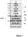
- MTJs comprise essentially two magnetic electrode layers separated by a thin tunnel barrier that most often is made of MgO. The magnetization of one of the magnetic electrodes is fixed by a synthetic antiferromagnetic layer SAF while the magnetization of the other electrode (called free layer or storage layer SL) can be switched to parallel or antiparallel alignment with that of the fixed layer.
- the fixed layer is also called a polarizer layer PL.
- a typical structure of a MTJ is showed in figure 1 .
- the switching of the SL magnetization is induced by a current of sufficiently large amplitude flowing vertically through the stack upwards or downwards by using spin transfer torque.
- the magnetic state of the memory element is read out by using the tunnel magnetoresistance TMR of the MTJ.
- Parallel magnetic configuration usually yields a lower resistance than the antiparallel configuration.
- MgO based MTJs exhibit a large TMR amplitude exceeding 200% with practical perpendicular MTJ stacks at room temperature and even up to 600% in some cases.
- This large TMR is obtained thanks to the bcc (body cubic centered) coherent crystalline nature of both the CoFe alloy based magnetic electrodes and of the MgO barrier.
- This crystalline coherence yields a spin-filtering effect associated with the symmetry of the electron wave-functions. This additional spin-filtering mechanism is responsible for the large TMR of these junctions.
- a stack appropriate for magnetic random access memories (MRAM) applications must satisfy a number of requirements both from magnetic and transport points of view.
- Concerning the magnetic properties it must exhibit a strong pinning of the polarizer layer PL to make sure that its magnetization does not switch during operation as well as a high thermal stability of the storage layer SL magnetization to ensure the required memory retention but still having the ability to switch the storage layer magnetization with minimum current density.
- Concerning the electrical properties, the MTJ stack must have a TMR amplitude as large as possible, preferably above 200% and even higher for high density memory applications (several Gbits) as well as resistancexarea RA product adjusted so as to approximately match the resistance of the selection transistor in passing mode (i.e. RA product in the range of 3 to 10 ⁇ . ⁇ m 2 but decreasing as the memory dot size decreases).
- MgO based magnetic tunnel junctions MTJ The process of deposition and annealing of MgO based magnetic tunnel junctions MTJ is well known by the man skilled in the art. An example of such a magnetic tunnel junction MTJ is shown in figure 1 .
- the layers have a magnetization perpendicular to their plane.
- the storage layer SL consists here of 1.5nm CoFeB/ 0.3nm Ta/ 1.4nmCoFeB.
- the storage layer SL is sandwiched between two MgO tunnel barriers to increase the perpendicular anisotropy of the storage layer arising from the CoFeB/MgO interfaces.
- the cap layer is here non-magnetic.
- Amorphous CoFeB alloys are used as electrode material in contact with the MgO barrier.
- the stacks are subsequently annealed at elevated temperature (typically in the range 300-400°C) to improve the crystallization of the MgO barrier into (100) bcc structure and induce the crystallization of the CoFeB alloy from the MgO interface towards the bulk of the layers.
- the CoFeB layers crystallize in a bcc structure which matches the (100) bcc structure of MgO. This results in a nice crystalline coherence between the CoFe based magnetic electrodes and the MgO barrier which is required to get a large TMR amplitude.
- the growth planes (parallel to the CoFeB/MgO interfaces) have a 4-fold symmetry.
- the B has to be expelled out of the CoFeB layer. This is achieved by introducing in the stack a B absorbing layer in direct contact with the CoFeB layer at the interface opposite to the CoFeB/MgO interface.
- the most widely used B absorbing layer is made of Ta but Mo, W or Hf have also been proved to work.
- magnetic tunnel junctions MTJs can be developed with in-plane or out-of-plane magnetization.
- out-of-plane magnetized MTJs are used because they offer better trade-off between thermal stability of the storage layer SL and write current than their in-plane counterpart.
- the polarizer layer PL In these out-of-plane magnetized MTJs (also called perpendicular MTJs, noted pMTJs), the polarizer layer PL must have a strong perpendicular anisotropy so that the polarizer layer keeps a stable magnetization during all the memory life time.
- the polarizer layer PL is usually coupled through the thin B absorbing layer to another layer called pinning layer Pl having strong perpendicular anisotropy (typically a (Co/X) based multilayer), where X represents Pt, Pd or Ni metals.
- pinning layer Pl having strong perpendicular anisotropy (typically a (Co/X) based multilayer), where X represents Pt, Pd or Ni metals.
- a synthetic antiferromagnetic reference layer SAF with perpendicular anisotropy pSAF is usually used in the stack.
- the conventional pSAF layer in perpendicular tunnel junction stacks pMTJs comprises two sets of Co/X multilayers ML1, ML2 anti-ferromagnetically coupled through a thin Ru layer called an antiferromagnetic coupling layer (AFC) via RKKY interactions.
- Ru layer thickness is typically between 0.4 and 0.8nm to provide the antiferromagnetic coupling.
- These Co/X multilayers generally have a cubic face centered fcc structure and grow by sputtering in the (111) direction. As a result, the growth planes have a 3-fold symmetry.
- in-plane magnetized MTJs the same problem of structural transition between fcc and bcc parts of the stack exists.
- the pinning of the in-plane synthetic antiferrromagnetic reference layer SAF is usually achieved by the phenomenon of exchange bias obtained by coupling one of the ferromagnetic layer of the SAF to an antiferromagnetic layer (most often made of Ir20Mn80, about 5 to 8nm thick) which has a fcc structure. Therefore, a structural symmetry breaking layer must be introduced between the pinned part of the stack and the polarizer layer to allow the structural transition from fcc to bcc.
- Synthetic antiferromagnetic reference layers SAF for in-plane magnetized MTJs have commonly composition of the form: buffer layer /IrMn 7nm /CoFe 2.5nm/Ru 0.8nm/CoFe 1nm/structural symmetry breaking layer 0.3nm/CoFeB 1.8nm/tunnel barrier,
- the layer above the Ru spacer does not contain a Co/X multilayer. It is directly the antiferromagnetic coupling with the multilayer below the Ru spacer plus the interfacial perpendicular anisotropy at the CoFeB/MgO interface which pulls the magnetization of the soft layer and polarizer layer (here Co/Ta/CoFeB) out-of-plane.
- this pSAF layer does not show sharp magnetic reversal with high squareness after annealing at 400 °C temperature. This is most likely due to interdiffusion of symmetry breaking material (for instance Ta) into the CoFeB layers.
- Ta indeed easily diffuses into CoFeB alloys above 300°C preferentially along the grain boundaries during the annealing process.
- Ta and an alloy based on Fe, Co and Ta were used as symmetry breaking layer to ensure the transition from fcc (111) to bcc (001) CoFeB polarizer layer.
- the patent US 8,860,156 B2 does not report anything about the annealing stability of the pSAF layers.
- the RKKY coupling layer Ru and symmetry breaking layer were separated by a Co dusting layer.
- US2012294079 teaches an AFM coupling bilayer of Ta/Ru, for example.
- the invention aims to at least partially solve these drawbacks with a new trifunctional non-magnetic multilayer structure TriAF used to achieve three functions: i) to antiferromagnetically couple two ferromagnetic layers in a SAF, ii) to insure a structural symmetry transition within the SAF stack and iii) to absorb the B out of the ferromagnetic layer adjacent to the tunnel barrier.
- TriAF used to achieve three functions: i) to antiferromagnetically couple two ferromagnetic layers in a SAF, ii) to insure a structural symmetry transition within the SAF stack and iii) to absorb the B out of the ferromagnetic layer adjacent to the tunnel barrier.
- the advantage of this TriAF compared to the state of the art SAF is to provide an ultrathin antiferromagnetic synthetic layer SAF.
- the SAF according to the invention is thinner than the standard SAF used in magnetic tunnel junction MTJ and greatly reduces the issues due to the redeposition of the etch
- the magnetic tunnel junctions MTJs obtained thanks to the synthetic antiferromagnetic layer SAF according to the invention show then an increased production yield, an enhanced magnetoresistance amplitude, and a reduced dot to dot variability.
- the invention has for object a synthetic antiferromagnetic layer SAF according to the independent device claim 1.
- a synthetic antiferromagnetic layer SAF according to the invention can have an in-plane magnetization or an out of plane magnetization.
- the latter is also known as a perpendicular synthetic antiferromagnetic layer or pSAF.
- An amorphizing element shall be understood according to the invention as a chemical element adapted to transform a crystalline structure into a at least partially or totally amorphous structure.
- Said amorphizing element may be for instance Boron B or zirconium Zr.
- the non-magnetic structure TriAF is named a trifunctional layer because it has three functions. First, in case where the amorphizing element is Boron, it acts as a Boron scavenger attracting the boron out of the first ferromagnetic layer in contact with the MgO tunnel barrier TB upon annealing of the stack.
- the bcc (100) crystallinity of the MgO tunnel barrier is improved and induces the crystallization of the CoFeB PL layer from the interface towards the bulk of the structure. Simultaneously Boron is expelled out from the CoFeB PL layer to the TriAF layer which facilitates bcc (100) crystallization of CoFeB PL.
- the TriAF layer is adapted to absorb the boron expelled out of the PL layer upon annealing.
- the polarized layer PL has a 4-fold symmetry bcc structure while the hard layer HL has a 3-fold symmetry fcc structure.
- This trifunctional coupling layer TriAF suppresses the need for an extra ferromagnetic layer and symmetry breaking layer SBL between the antiferromagnetic coupling layer (Ru for instance) and the CoFeB reference layer.
- the synthetic antiferromagnetic layer SAF comprising the trifunctional non-magnetic multi-layered structure TriAF is very thin.
- the proposed synthetic antiferromagnetic layer SAF removes two distinct layers in prior art magnetic stacks: the magnetic layer between Ru RKKY coupling layer and PL layer (it can be Co dusting layer or Co/X multilayers) and the symmetry breaking layer SBL which serves also as Boron absorber layer.
- the obtained synthetic antiferromagnetic SAF layer is thinner than the synthetic antiferromagnetic layers of the prior art.
- the resulting magnetic tunnel junction MTJ has a reduced thickness which accounts for a higher production yield, reduced dot-to-dot variability and enhanced tunnel magnetoresistance TMR amplitude.
- the thickness of the SAF stack can be reduced by 1.3 to 1.6nm compared to the thickness of state of the art SAF.
- the materials used in this trifunctional antiferromagnetic coupling layer TriAF also minimize the risks of interdiffusion up to 400 °C annealing temperature thus allowing to reach higher TMR amplitude thanks to higher possible annealing temperatures.
- the proposed SAF layer allows back-end-of-line process fabrication of spintronic devices.
- this trifunctional coupling layer TriAF allowing to reduce the thickness of the pinned layer is particularly important for MTJ based MRAM, including STT-MRAM, spin-orbit torque MRAM (SOT-MRAM), voltage controlled MRAM, for which the patterning of very small MTJs (sub-20nm) is required to reach high memory densities (Gbit range).
- a SAF layer can also be used in all spintronic devices in which a SAF layer have to be formed associated with a structural transition within the SAF, in particular in magnetic-field sensors based on MTJ and in spin transfer torque oscillators, spin orbit torque oscillators or spin-diodes.
- the synthetic antiferromagnetic layer SAF according to the invention includes one or more additional characteristics from those listed in the following:
- the non-magnetic multi-layered structure TriAF comprises a bilayer comprising a first C non-magnetic layer and a second T non-magnetic I layer.
- a second object of the present invention is a magnetic tunnel junction MTJ comprising the synthetic antiferromagnetic layer SAF according to the invention, a first tunnel barrier TB layer and a storage layer SL and/or a second tunnel barrier layer such as a MgO layer added in contact with the storage layer SL on its interface opposite to the first tunnel barrier.
- the first and second tunnel barrier layer TB may be made of MgO. But other materials such as for instance MgAl 2 O 4 may also be used for the first and second tunnel barrier.
- the resulting magnetic tunnel junction MTJ has a reduced thickness which is useful in reducing the redeposition of impurities following the etching process, increasing the production yield, enhancing the tunnel magnetoresistance and reducing the dot to dot variability.
- the magnetic tunnel junction MTJ is particularly adapted for SOT-MRAM since the free layer has to be in contact with an horizontal conducting line having high spin orbit constant.
- the magnetic tunnel junction MTJ according to the invention may include one or more additional characteristics from those listed in the following, either individually or in any technical possible combination thereof:
- Another object of the invention is a spintronic device including a synthetic antiferromagnetic SAF layer comprising a trifunctional layer TriAF according to the invention.
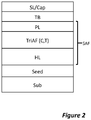
- Figure 2 shows a first example of a synthetic antiferromagnetic SAF layer comprising a trifunctional non-magnetic multi-layer structure TriAF according to the present invention.
- Figure 2 shows that the synthetic antiferromagnetic layer SAF according to the invention comprises:
- the magnetic stack shown in figure 2 comprises the following layers (from bottom to top): a substrate layer SUB, a seed layer on top of the SUB layer, the synthetic antiferromagnetic layer SAF according to the invention, a tunnel barrier TB on the top of the SAF layer, a storage layer SL and a cap layer above the storage layer. This forms a magnetic tunnel junction MTJ.
- the structure is called a perpendicular synthetic antiferromagnet pSAF.
- the first ferromagnetic layer PL can act as a polarizer or reference layer.
- the polarizing layer PL can be a CoFeB alloy layer or a CoFe based alloy layer or an Heusler alloy layer or a combination of such layers.
- the hard layer HL comprises n bilayers of A/X nano-laminates which have intrinsic perpendicular magnetic anisotropy PMA originated from A/X interfaces via electron hybridization effect or interfacial strain.
- the material for A can be made of Co, Fe, CoFe, CoFeB or an alloy thereof, and X is Pt, Au, Ir, Pd, Ni, NiCo, NiFe or NiFeCo based alloys. Similar PMA can be obtained if A and X are interchanged to form X/A nano-laminates.
- the hard layer HL may also be a material exhibiting bulk PMA, for example L1 0 ordered alloy of Fe-Pt, Fe-Pd and Co-Pt; L1 1 ordered alloy CoPt, CoPd, Co-Ni-Pt. It may also be an alloy of rare earth-transition metals in the form of RE-TM where RE stands for Tb, Dy, Er, Gd or an alloy thereof, and TM stands for Fe, Co or an alloy thereof. It can also be a Heusler alloy with perpendicular anisotropy such as Mn2.7Co0.3Ga.
- the hard layer HL is preferably an exchange biased layer i.e. a ferromagnetic layer essentially made of a CoFe alloy 1.5 to 3 nm thick which is exchange coupled to an antiferromagnetic layer most often made of IrMn typically between 5nm and 8nm thick or PtMn typically 10nm to 20nm thick.
- an exchange biased layer i.e. a ferromagnetic layer essentially made of a CoFe alloy 1.5 to 3 nm thick which is exchange coupled to an antiferromagnetic layer most often made of IrMn typically between 5nm and 8nm thick or PtMn typically 10nm to 20nm thick.
- the trifunctional coupling layer TriAF of the synthetic antiferromagnetic layer SAF ensures three functions: the first is to provide antiferromagnetic coupling between the hard layer HL and the reference layer PL.
- the second function is to ensure a structural transition between two layers of different structural symmetry for instance here the fcc structure of the hard layer HL and the bcc structure of the reference or polarizer layer PL.
- the third function is absorption of boron from CoFeB polarizer layer PL upon annealing.
- the HL and the polarizer layer PL are antiferromagnetically coupled by the trifunctional anti-ferromagnetic TriAF coupling layer.
- the TriAF coupling layer consists of a C/T bilayer where C is one of Ru, Re, Rh, Ir, Cu and Os or an alloy thereof. The thickness of this C layer is adjusted in the range 0.2nm-0.9nm together with that of the T layer to provide a strong RKKY interaction between HL and PL through the C/T composite layer.
- T is one of W, Mo, Nb, V,
- Ta, Cr or an alloy thereof which functions as a symmetry breaking layer allowing the structural transition from the HL layer.
- the hard layer HL and the polarizer layer have usually different crystal structures.
- the hard layer HL can have a fcc crystal structure as for Co/Pt type multilayers or exchange biased IrMn/CoFe bilayers, or tetragonal as with FePt L1 0 .
- the polarizer layer PL can have a bcc (001) crystal structure like CoFeB.
- the T layer can also act as inter-diffusion barrier between the C layer and the PL layer and/or as a partial B getter layer.
- the thickness of the T layer is also adjusted in the range (0.1-0.6nm) together with that of the C layer to provide strong antiferromagnetic coupling between HL and PL through the C/T composite layer.
- the TriAF coupling layer can be a multilayer formed with (C/T)n configuration with T on top. This means that the TriAF layer is formed by n bilayers of C/T bilayers. Since the C/T bilayers play the three functions of coupling, symmetry breaking and B absorption, this stack of layers acts as a trifunctional anti-ferromagnetic coupling layer (TriAF).
- the tunnel barrier can be one of MgO, AlOx, TaOx, Ti02, HfOx, ZrOx, GaOx, SrTi03 or other metal oxide on top of pSAF layer which generate interface perpendicular magnetic anisotropy with PL and SL and provides large TMR amplitude.
- Figure 3 shows the variation of the magnetization M of a synthetic antiferromagnetic layer SAF as a function of the applied magnetic field H varying from positive saturation to negative saturation.
- This represents the descending branch of the M-H hysteresis loop.
- the ascending branch is not represented.
- the ascending branch would be symmetric of the descending one with respect to the origin of the graph.
- the y axis represents the measured magnetization expressed in electromagnetic unit and the x axis represents the applied magnetic field in Oe (1 Oe equals 79,77 A/m).
- the SAF/MgO/cap measured sample has the composition Pt / (Co/Pt)3/Co / Ru 4 ⁇ / W 2 ⁇ / CoFeB 10 ⁇ / MgO / Cap and was annealed at 340 °C.
- the M-H loop was measured by vibrating sample magnetometer VSM. Along this descending branch of hysteresis loop, the field is decreased from the positive saturation to the negative saturation. Three magnetization reversal steps are observed while decreasing the field from positive to negative saturation as described below. All the magnetization reversal steps with the sweeping of magnetic field are sharp with high squareness. This signifies that the SAF layer has perpendicular anisotropy. Coming from high saturation positive field, the first reversal around 341 kA/m s the characteristic field
- the switching of the CoFeB layer at 341 kA/m is driven by the RKKY antiferromagnetic coupling against the applied field whereas the switching at - 363 kA/m s driven by the applied field against the antiferromagnetic RKKY coupling.
- a characteristic field Ho can then be defined as (H 0+ - H 0- )/2 called inter-layer exchange coupling field or RKKY coupling field. It is equal here to 348 kA/m.
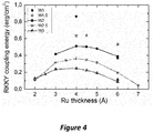
- Figure 4 shows the RKKY coupling energy of the SAF versus thicknesses of the different layers of the TriAF layer.
- the material configuration of the SAF is Pt / (Co/Pt)3/Co / Ru (x) / W (y) / CoFeB 10 ⁇ / MgO, where x and y respectively represent the thicknesses of Ru and W in Angstroms.
- Figure 4 shows the variation of coupling energy as a function of Ru thickness for different thicknesses of W in Angstroms.
- the y axis of figure 4 represents the RKKY coupling energy expressed in erg/cm 2 .
- the x axis represents the thickness of the Ru layer.
- Each set of points in figure 4 represents a different thickness of the W layer.
- the coupling energy can be tuned over a broad range.
- Ru thickness in the range of 0.4 to 0.45 nm which is the thickness region for the first peak of the oscillatory curve of RKKY coupling energy.
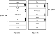
- the MTJ stack (either in-plane or out-of-plane magnetized) can be configured as top free or bottom free layer configuration as shown for example in Figures 5a and b respectively in the case of out-of-plane magnetized MTJ.
- the top free layer configuration of the magnetic tunnel junction MTJ of figure 5a comprises the following layers from the bottom to the top of the stack: a substrate layer SUB, a seed layer, a perpendicular antiferromagnetic synthetic layer pSAF according to the invention, a MgO tunnel barrier, a storage layer SL and a cap layer.
- the pSAF according to the invention showed in figure 5a comprises the following layers from bottom to top: a hard layer HL on the top of the seed layer of the MTJ, a non-magnetic multi-layered structure TriAF on the top of the HL layer and a polarizing layer PL on the top of the TriAF layer, the PL layer being below the MgO tunnel barrier of the MTJ.
- the bottom free layer configuration of the magnetic tunnel junction MTJ of figure 5b comprises the following layers from the bottom of the stack to the top of the stack: a substrate layer SUB, a seed layer, a storage layer SL, a MgO tunnel barrier, a perpendicular antiferromagnetic synthetic layer pSAF according to the invention and a cap layer.
- the pSAF according to the invention shown in figure 5b comprises the following layers from bottom to top: a polarizing layer PL placed on top of the MgO layer of the MTJ, a non-magnetic multi-layered structure TriAF on top of the polarizing layer PL and a hard layer HL on top of the TriAF layer, the HL layer being below the Cap layer of the MTJ.
- the MgO tunnel barrier can be prepared by RF deposition of MgO from an MgO target or by natural oxidation of a metallic Mg layer.
- the free layer SL can be made of CoFeB alloy or be a composite layer consisting of a stack of several layers of different (Co1-xFex)1-yBy compositions (x between 0 and 1 and y between 0 and 0.3).
- perpendicular MTJ In perpendicular MTJ, as known by the man skilled in the art, provided this layer is thin enough ( ⁇ 1.6 nm), its magnetization is pulled out-of-plane by the interfacial anisotropy which exists at the interface between the storage layer and the MgO barrier. But other materials exhibiting perpendicular anisotropy and low Gilbert damping ( ⁇ 0.02) could be used as storage layer or free layer SL in particular among the Heusler alloys.
- the cap layer Cap is in contact with the storage layer SL. It is a non-magnetic metal which must have the ability to absorb the B from the storage layer SL upon annealing. It can be made of Ta but also Mo, W, Ru or other non-magnetic species having the ability to absorb B out of CoFeB upon annealing. Concerning the TriAF layer which is coupling the hard layer HF to the polarizer layer PL, it can be here of the form C/T with the Boron getter layer T above the C layer i.e. in contact with the Boron doped electrode.
- the cap layer is Cap in contact with the hard layer HL.
- the hard layer HL usually does not contain B, the requirement for this cap layer Cap to be able to absorb B is relieved.
- the cap layer Cap can still be made of Ta, Ru, W, Mo with other existing possibilities such as Cu, Ti, Au, Pd, Pt, Hf.
- Similar stacks with bottom free or top free layer can be considered with in-plane magnetized materials.
- the HL is an exchange biased layer as previously described and the storage layer SL is chosen with in-plane magnetization.
- This can be achieved by using also CoFeB layer but with a larger thickness than in the perpendicular anisotropy case so that the easy-plane demagnetizing energy exceeds the interfacial perpendicular MgO/CoFeB anisotropy resulting in an in-plane magnetization of the layer.
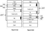
- Figures 6 (a) and (b) show another embodiment of the magnetic tunnel junction MTJ according to the invention.
- the magnetic tunnel junction MTJ of figure 6a comprises the following layers from bottom to top: a substrate layer SUB, a seed layer, a perpendicular synthetic antiferromagnetic layer pSAF according to the invention, a first MgO layer, a composited storage layer CSL, a second MgO layer and a Cap layer.
- the pSAF layer of figure 6a comprises from bottom to top: a hard layer HL on top of the Seed layer of the MTJ, a trifunctional non-magnetic multi-layered structure TriAF and a polarizer layer PL below the first MgO layer.
- the composite storage layer (CSL) of figure 6a comprises two ferromagnetic FM layers ferromagnetically coupled through a thin B absorbing layer or NM layer.
- the magnetic tunnel junction of figure 6b comprises the following layers from bottom to top: a substrate layer Sub, a seed layer, a second MgO layer, a composite storage layer CSL, a first MgO layer, a perpendicular antiferromagnetic layer pSAF according to the invention and a cap layer.
- the pSAF layer of figure 6b comprises from bottom to top: a polarizer layer PL above the second MgO layer, a trifunctional non-magnetic multi-layered structure TriAF and a hard layer HL below the cap layer of the MTJ.
- a peculiarity of these stacks is that they also comprise a second MgO layer added in contact with the composite storage layer CSL on its interface opposite to the first MgO tunnel barrier.
- This type of stacks is especially interesting in the case of out-of-plane magnetized MTJs since the second MgO layer allows to further increase the perpendicular anisotropy of the composite storage layer CSL. This increases the thermal stability factor of the composite storage layer CSL and therefore retention of memory devices. This also allows to increase the CSL thickness (typically from 1.3nm to 3nm) resulting in an enhanced TMR amplitude.
- NM is generally a non-magnetic layer.
- the NM layer is intended to absorb the B away from the MgO interfaces.
- NM can be made of B absorbing materials such as Ta, W, Ru, Mo, or an alloy or MLs thereof.
- NM may also comprise some magnetic elements such as Co and Fe to increase the magnetic coupling across it.
- NM may be slightly magnetic.
- This layer must be thick enough to be able to absorb a sufficient amount of B from the adjacent CoFeB layers but must be thin enough to still ensure a good magnetic coupling (ferromagnetic or antiferromagnetic depending on its thickness) between the two magnetic layers on both sides of it. Its thickness is typically in the range 0.2nm to 1nm.
- the storage layer can be made of Heusler alloys with perpendicular anisotropy and low damping.
- the cap layer Cap above the 2nd MgO layer in the stack of Figure 6 a is non-magnetic. It can be made for instance of Ru, W, Mo, Ta.
- the seed layer below the second MgO layer in Fig.6b is a non-magnetic one. It can be made of Ta or another material favoring the bcc growth of MgO such as W or Cr.
- a top free perpendicular MTJ stack as described in Figure 6(a) was deposited.
- the material configuration for the stack was Pt/(Co/Pt)3/Co/Ru 4 ⁇ /W 2 ⁇ /CoFeB 10 ⁇ /MgO/Composite Storage layer/MgO/Cap. Its hysteresis loop was measured by vibrating sample magnetometry (VSM) after annealing at 400 °C.
- the measured hysteresis loop is shown in Figure 7 .
- the y axis of figure 7 represents the measured magnetization of the stack, expressed in electromagnetic unit.
- the x axis of figure 7 represents the applied magnetic field expressed in Oe (1 Oe equals 79,77 A/m). Coming from high positive field, the polarizer layer PL magnetization switches first at 249 kA/m.
- the field is reversed and with a very small negative field -3,2 kA/m the free layer magnetization is oriented along the field.
- a characteristic field (-80 kA/m) where magnetization of both PL and HL switch simultaneously (coercive field of the antiferromagnetically coupled sandwich formed by the HL/TriAF/PL).
- the PL magnetization switches at -259 kA/m to align with the applied magnetic field.
- the minor loop of polarized layer across the dotted line at 258 kA/m shows a sharp vertical reversal with coercivity of 10 kA/m. This means that at high annealing temperature (400 °C), the perpendicular magnetic anisotropy PMA of PL and its strong RKKY coupling to the HL are preserved by the TriAF coupling layer.
- Figure 8 shows another embodiment of dual magnetic tunnel junction MTJ stack comprising two proposed thin SAF layers each using a trifunctional coupling layer TriAF.
- a top perpendicular synthetic antiferromagnetic layer SAF and a bottom perpendicular synthetic antiferromagnetic layer SAF are used.
- the stack of figure 8 comprises the following layers from bottom to top: a substrate layer Sub, a seed layer, a bottom SAF, a first MgO layer, a composite storage layer CSL, a second MgO layer, a top SAF and a cap layer.
- the bottom SAF of figure 8 comprises the following layers from bottom to top: a hard layer HL, a trifunctional non-magnetic multi-layered structure TriAF and a polarizing layer PL, the polarizing layer being below the first MgO layer.
- the top SAF of figure 8 comprises an additional polarizing layer APL, a trifunctional non-magnetic multi-layered structure TriAF and a second hard layer HL, the second hard layer HL being below the cap layer.
- the layer above the second MgO barrier is here a magnetic additional polarizing layer APL whereas it is a non-magnetic layer in the embodiment depicted in Figure 6 .
- the purpose of this additional polarizing layer APL is to further increase the spin transfer efficiency by combining the spin transfer torque acting on the storage layer CSL magnetization originating from the first polarizing layer PL with the spin transfer torque originating from this additional polarizing layer APL.
- This APL layer can be CoFeB, or other magnetic material with high spin polarization.
- the polarizer layer PL can be antiferromagnetically coupled to a hard layer HL through a TriAF layer to increase its pinning energy.
- the additional polarizing layer APL can be antiferromagnetically coupled to a second hard layer HL through a TriAF layer to increase its pinning energy.
- the advantages of using such bottom and top SAF layers is to reduce the magnetostatic coupling that they may have between them as well as with the storage layer CSL.
- the storage layer CSL is composite and consists of a ferromagnetic/non-magnetic/ferromagnetic or FM/NM/FM sandwich where the magnetizations of the two ferromagnetic layers are ferromagnetically coupled though the non-magnetic spacer (the latter can be made of Ta, W, Mo typically 0.1 to 1nm thick).
- the magnetization of the CoFeB polarizer layer and of the 2nd polarizer layer must be set in antiparallel alignment to obtain the maximum STT efficiency.
- setting these magnetizations in antiparallel alignment can be achieved by performing minor hysteresis loops taking advantage of the difference of coercivity of the two polarizer layers.
- the two MgO barriers must have different resistance x area RA products since the changes of resistance associated with CSL magnetization switching from the bottom MgO barrier and from the top MgO barrier are opposite in sign. Indeed, when there is parallel magnetic alignment across one barrier, the other is in antiparallel alignment and vice versa. Since these two tunnel barriers can be considered as connected in series, using MgO barriers of different RA allows not to reduce excessively the net tunnel magnetoresistance of the stack. Typically, a difference of RA product by at least a factor 3 is desirable.
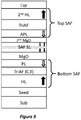
- Figure 9 shows another embodiment of the magnetic tunnel junction MTJ according to the invention.
- the stack of figure 9 comprises the following layers from bottom to top: a substrate layer Sub, a seed layer, a bottom synthetic antiferromagnetic layer SAF, a first MgO layer, a synthetic antiferromagnetic storage layer SAF SL, a second MgO layer, a top SAF and a cap layer.
- the bottom SAF of figure 9 comprises a hard layer HL placed above the seed layer, a trifunctional non-magnetic multilayered structure TriAF, a polarizing layer PL below the first MgO layer.
- the top SAF of figure 9 comprises from bottom to top an additional polarized layer APL placed above the second MgO layer, a trifunctional non-magnetic multilayered structure TriAF and a second hard layer HL below the cap layer.
- the storage layer SAF SL instead of being made of a composite ferromagnetic layer, is made of a synthetic antiferromagnetic layer SAF of the form ferromagnetic/non-magnetic/ferromagnetic in which the two ferromagnetic layers are antiferromagnetically coupled through the non-magnetic layer.
- the later can be made for instance of TriAF, Ta, W, Mo or Ru with thickness chosen so as to get antiferromagnetic coupling.
- the polarizer layer PL and the additional polarizing layer APL must then be set in parallel magnetic configuration to get the maximum spin transfer efficiency.
- Another object of the invention is a spintronic device comprising a synthetic antiferromagnetic SAF layer comprising a trifunctional layer TriAF according to the invention.
- Such a device can be for example a Spin Transfer Torque Magnetic Random Access Memory STT-MRAM, a Spin Orbit Transfer Magnetic Random Access Memory SOT-MRAM, a Spin transfer oscillator, a spin-diode, a memristor or a magnetoresistive sensor.
- the magnetic tunnel junction of figure 5b is particularly adapted to a SOT-MRAM due to the accessibility of the storage layer SL.
- the magnetic tunnel junctions described in Figures 5a , 6a , 6b , 8 and 9 are particularly adapted for STT-MRAM applications.
Landscapes
- Engineering & Computer Science (AREA)
- Computer Hardware Design (AREA)
- Chemical & Material Sciences (AREA)
- Crystallography & Structural Chemistry (AREA)
- Power Engineering (AREA)
- Hall/Mr Elements (AREA)
- Mram Or Spin Memory Techniques (AREA)
Claims (9)
- Synthetische antiferromagnetische Schicht (SAF, pSAF) in einem SOT-MRAM, umfassend:- eine erste ferromagnetische Schicht (PL), die ein amorphisierendes Element enthält, wobei die erste ferromagnetische Schicht (PL) eine erste strukturelle Symmetrie aufweist;- eine zweite ferromagnetische Schicht (HL) mit einer zweiten strukturellen Symmetrie; wobei die synthetische antiferromagnetische Schicht (SAF, pSAF) umfasst, dass die erste und die zweite ferromagnetische Schicht durch eine nicht-magnetische Mehrschichtstruktur (TriAF) antiferromagnetisch gekoppelt sind, wobei die antiferromagnetische Kopplung eine RKKY-Kopplung ist, dadurch gekennzeichnet, dass die nicht-magnetische Mehrschichtstruktur mindestens eine Doppelschicht umfasst, wobei jede Doppelschicht eine erste (C) nicht-magnetische Schicht und eine zweite (T) nicht-magnetische Schicht umfasst, wobei die erste (C) nicht-magnetische Schicht eines der Elemente Ru, Re, Rh, Cu, Ir, Os oder eine Legierung davon umfasst und die zweite (T) nicht-magnetische Schicht eines der Elemente W, Mo, Nb, Ta, V, Cr oder eine Legierung davon umfasst.
- Synthetische antiferromagnetische Schicht (SAF, pSAF) gemäß dem vorherigen Anspruch, dadurch gekennzeichnet, dass die Dicke der ersten (C) nichtmagnetischen Schicht weniger als 2 nm beträgt und vorteilhafterweise zwischen 0,2 nm und 0,9 nm liegt.
- Synthetische antiferromagnetische Schicht (SAF, pSAF) nach einem der vorherigen Ansprüche, dadurch gekennzeichnet, dass die Dicke der zweiten (T) nicht-magnetischen Schicht weniger als 1 nm beträgt und vorteilhafterweise zwischen 0,1 nm und 0,6 nm liegt.
- Magnetische Tunnelverbindung (MTJ), umfassend die synthetische antiferromagnetische Schicht (SAF/pSAF) nach einem der vorherigen Ansprüche, eine erste Tunnelbarriereschicht, wie eine MgO-Schicht, eine Speicherschicht (SL) und eine Deckschicht und/oder eine zweite Tunnelbarriereschicht, wie eine MgO-Schicht, die in Kontakt mit der Speicherschicht (SL) an ihrer der ersten Tunnelbarriereschicht gegenüberliegenden Grenzfläche hinzugefügt ist.
- Magnetische Tunnelverbindung (MTJ) gemäß dem vorherigen Anspruch, dadurch gekennzeichnet, dass die Speicherschicht eine Verbundspeicherschicht (CSL) ist, wobei die Verbundspeicherschicht einen Stapel umfasst, der aus mindestens einer ersten ferromagnetischen Schicht (FM), einer nicht-magnetischen Schicht oder Mehrfachschicht (NM) und einer zweiten ferromagnetischen Schicht (FM) gebildet ist, wobei die erste und die zweite ferromagnetische Schicht mindestens eine der folgenden Legierungen CoFeB, FeB, CoFe umfassen und die nicht-magnetische Schicht oder Mehrfachschicht so ausgelegt ist, dass sie das amorphisierende Element absorbiert und mindestens eines der folgenden Elemente Ta, W, Mo, Ru oder eine Legierung davon umfasst.
- Magnetische Tunnelverbindung (MTJ) nach Anspruch 4 oder 5, dadurch gekennzeichnet, dass sie eine zusätzliche magnetische Schicht (APL), die in Kontakt mit der zweiten Tunnelbarriereschicht hinzugefügt ist, und/oder eine zusätzliche synthetische antiferromagnetische Schicht (SAF, pSAF) in Kontakt mit der zweiten Tunnelbarriereschicht umfasst.
- Magnetische Tunnelverbindung (MTJ) nach Anspruch 6, dadurch gekennzeichnet, dass die zusätzliche synthetische antiferromagnetische Schicht eine zusätzliche trifunktionale nicht-magnetische Mehrschichtstruktur (TriAF) umfasst.
- Magnetische Tunnelverbindung (MTJ) nach Anspruch 6 oder 7, dadurch gekennzeichnet, dass die Speicherschicht SL durch eine synthetische antiferromagnetische Schicht (SAF SL) gebildet ist.
- Spintronische Vorrichtung mit einer synthetischen antiferromagnetischen Schicht SAF nach einem der Ansprüche 1 bis 3.
Priority Applications (2)
| Application Number | Priority Date | Filing Date | Title |
|---|---|---|---|
| EP17306063.3A EP3442042B1 (de) | 2017-08-10 | 2017-08-10 | Synthetische antiferromagnetische schicht, magnetische tunnelverbindung und spintronische vorrichtung mit verwendung der besagten synthetischen antiferromagnetischen schicht |
| US16/100,484 US10658574B2 (en) | 2017-08-10 | 2018-08-10 | Synthetic antiferromagnetic layer, magnetic tunnel junction and spintronic device using said synthetic antiferromagnetic layer |
Applications Claiming Priority (1)
| Application Number | Priority Date | Filing Date | Title |
|---|---|---|---|
| EP17306063.3A EP3442042B1 (de) | 2017-08-10 | 2017-08-10 | Synthetische antiferromagnetische schicht, magnetische tunnelverbindung und spintronische vorrichtung mit verwendung der besagten synthetischen antiferromagnetischen schicht |
Publications (2)
| Publication Number | Publication Date |
|---|---|
| EP3442042A1 EP3442042A1 (de) | 2019-02-13 |
| EP3442042B1 true EP3442042B1 (de) | 2020-12-09 |
Family
ID=59856465
Family Applications (1)
| Application Number | Title | Priority Date | Filing Date |
|---|---|---|---|
| EP17306063.3A Active EP3442042B1 (de) | 2017-08-10 | 2017-08-10 | Synthetische antiferromagnetische schicht, magnetische tunnelverbindung und spintronische vorrichtung mit verwendung der besagten synthetischen antiferromagnetischen schicht |
Country Status (2)
| Country | Link |
|---|---|
| US (1) | US10658574B2 (de) |
| EP (1) | EP3442042B1 (de) |
Families Citing this family (29)
| Publication number | Priority date | Publication date | Assignee | Title |
|---|---|---|---|---|
| US10734013B2 (en) * | 2017-10-03 | 2020-08-04 | Western Digital Technologies, Inc. | Spin transfer torque (STT) device with multilayer seed layers for magnetic recording and memory |
| US11387405B2 (en) * | 2017-11-27 | 2022-07-12 | Carnegie Mellon University | Resonance rotating spin-transfer torque memory device |
| US10388853B2 (en) * | 2017-12-29 | 2019-08-20 | Spin Memory, Inc. | Magnetic memory having a pinning synthetic antiferromagnetic structure (SAF) with cobalt over platinum (Pt/Co) bilayers |
| US11193989B2 (en) | 2018-07-27 | 2021-12-07 | Allegro Microsystems, Llc | Magnetoresistance assembly having a TMR element disposed over or under a GMR element |
| US11069853B2 (en) * | 2018-11-19 | 2021-07-20 | Applied Materials, Inc. | Methods for forming structures for MRAM applications |
| JP2020155442A (ja) * | 2019-03-18 | 2020-09-24 | キオクシア株式会社 | 磁気デバイス |
| EP3731289B1 (de) * | 2019-04-23 | 2024-06-12 | IMEC vzw | Magnetische tunnelkontaktvorrichtung |
| EP3757997A1 (de) | 2019-06-24 | 2020-12-30 | IMEC vzw | Spintronische vorrichtung mit einer synthetischen antiferromagnetischen hybriden speicherschicht |
| JP7107285B2 (ja) * | 2019-07-12 | 2022-07-27 | 株式会社村田製作所 | 磁性構造体および磁性構造体の製造方法 |
| CN112310271B (zh) * | 2019-07-25 | 2023-04-07 | 上海磁宇信息科技有限公司 | 磁性随机存储器的磁性隧道结结构 |
| US11217626B2 (en) | 2019-08-30 | 2022-01-04 | Allegro Microsystems, Llc | Dual tunnel magnetoresistance (TMR) element structure |
| US11127518B2 (en) | 2019-08-30 | 2021-09-21 | Allegro Microsystems, Llc | Tunnel magnetoresistance (TMR) element having cobalt iron and tantalum layers |
| DE102019126320B4 (de) | 2019-09-30 | 2024-03-28 | Infineon Technologies Ag | Magnetoresistiver Sensor und Fertigungsverfahren für einen magnetoresistiven Sensor |
| CN112652704A (zh) * | 2019-10-10 | 2021-04-13 | 上海磁宇信息科技有限公司 | 具有超薄合成反铁磁层的磁性隧道结单元 |
| CN112736191A (zh) * | 2019-10-14 | 2021-04-30 | 上海磁宇信息科技有限公司 | 具有对称结构的磁性隧道结结构及磁性随机存储器 |
| CN112864306A (zh) * | 2019-11-12 | 2021-05-28 | 上海磁宇信息科技有限公司 | 具对称双势垒层的磁性隧道结结构及磁性随机存储器 |
| CN112864313B (zh) * | 2019-11-28 | 2023-03-21 | 上海磁宇信息科技有限公司 | 磁性随机存储器的磁性隧道结结构 |
| EP3836171B1 (de) | 2019-12-12 | 2024-04-10 | Imec VZW | Magnetischer dreischicht-abstandshalter zwischen einer magnetisch gepinnten oder harten schicht und einer magnetischen referenzschicht |
| US11081154B1 (en) * | 2020-01-27 | 2021-08-03 | Rongfu Xiao | Synthetic magnetic pinning element having strong antiferromagnetic coupling |
| US11088200B1 (en) * | 2020-02-10 | 2021-08-10 | Rongfu Xiao | Lattice matched seed layer to improve PMA for perpendicular magnetic pinning |
| EP3913386A1 (de) * | 2020-05-20 | 2021-11-24 | Crocus Technology S.A. | Magnetisches sensorelement und vorrichtung mit verbesserter genauigkeit unter hohen magnetfeldern |
| US11495737B2 (en) | 2020-06-29 | 2022-11-08 | United Microelectronics Corp. | Magnetic tunnel junction (MTJ) device |
| US11176981B1 (en) * | 2020-07-31 | 2021-11-16 | Western Digital Technologies, Inc. | Spinel containing magnetic tunnel junction and method of making the same |
| US11443790B2 (en) | 2020-07-31 | 2022-09-13 | Western Digital Technologies, Inc. | Spinel containing magnetic tunnel junction and method of making the same |
| US11217289B1 (en) | 2020-07-31 | 2022-01-04 | Western Digital Technologies, Inc. | Spinel containing magnetic tunnel junction and method of making the same |
| EP3961632A1 (de) | 2020-08-25 | 2022-03-02 | Commissariat à l'Energie Atomique et aux Energies Alternatives | Magnetischer tunnelübergang mit einer inhomogenen granulären freien schicht und zugehörige spintronikvorrichtungen |
| US11751483B2 (en) * | 2020-12-28 | 2023-09-05 | Globalfoundries Singapore Pte. Ltd. | Spin diode devices |
| CN114335329B (zh) * | 2022-03-16 | 2022-06-17 | 波平方科技(杭州)有限公司 | 一种具有高抗磁场干扰能力的磁性随机存储器 |
| EP4257998A1 (de) * | 2022-04-05 | 2023-10-11 | Commissariat à l'énergie atomique et aux énergies alternatives | Magnetoresistiver sensor mit empfindlichkeit gegen magnetfelder ausserhalb der ebene |
Citations (1)
| Publication number | Priority date | Publication date | Assignee | Title |
|---|---|---|---|---|
| US20120294079A1 (en) * | 2011-05-19 | 2012-11-22 | Sony Corporation | Memory element and memory device |
Family Cites Families (23)
| Publication number | Priority date | Publication date | Assignee | Title |
|---|---|---|---|---|
| US6723450B2 (en) * | 2002-03-19 | 2004-04-20 | Hitachi Global Storage Technologies Netherlands B.V. | Magnetic recording medium with antiparallel coupled ferromagnetic films as the recording layer |
| US7282277B2 (en) * | 2004-04-20 | 2007-10-16 | Seagate Technology Llc | Magnetic recording media with Cu-containing magnetic layers |
| US7099122B2 (en) * | 2003-12-16 | 2006-08-29 | Seagate Technology Llc | Spin polarization enhancement artificial magnet |
| JP4786331B2 (ja) * | 2005-12-21 | 2011-10-05 | 株式会社東芝 | 磁気抵抗効果素子の製造方法 |
| US8063459B2 (en) * | 2007-02-12 | 2011-11-22 | Avalanche Technologies, Inc. | Non-volatile magnetic memory element with graded layer |
| JP5150284B2 (ja) * | 2008-01-30 | 2013-02-20 | 株式会社東芝 | 磁気抵抗効果素子およびその製造方法 |
| JP5356431B2 (ja) * | 2011-02-17 | 2013-12-04 | 株式会社東芝 | 磁気抵抗効果素子、磁気ヘッドアセンブリ及び磁気記録装置 |
| US8860156B2 (en) | 2012-09-11 | 2014-10-14 | Headway Technologies, Inc. | Minimal thickness synthetic antiferromagnetic (SAF) structure with perpendicular magnetic anisotropy for STT-MRAM |
| US8796796B2 (en) * | 2012-12-20 | 2014-08-05 | Samsung Electronics Co., Ltd. | Method and system for providing magnetic junctions having improved polarization enhancement and reference layers |
| US8970991B2 (en) * | 2013-03-12 | 2015-03-03 | Seagate Technology Llc | Coupling feature in a magnetoresistive trilayer lamination |
| US9070381B1 (en) * | 2013-04-12 | 2015-06-30 | Western Digital (Fremont), Llc | Magnetic recording read transducer having a laminated free layer |
| US9121886B2 (en) * | 2013-09-25 | 2015-09-01 | Seagate Technology Llc | Magnetoresistive sensor including an amorphous insertion layer excluding glass former elements |
| US9230575B2 (en) * | 2013-12-13 | 2016-01-05 | Seagate Technology Llc | Magnetoresistive sensor with SAF structure having crystalline layer and amorphous layer |
| US9529060B2 (en) * | 2014-01-09 | 2016-12-27 | Allegro Microsystems, Llc | Magnetoresistance element with improved response to magnetic fields |
| US10297300B2 (en) * | 2014-09-21 | 2019-05-21 | Samsung Electronics Co., Ltd. | Method and system for determining temperature using a magnetic junction |
| US10074387B1 (en) * | 2014-12-21 | 2018-09-11 | Western Digital (Fremont), Llc | Method and system for providing a read transducer having symmetric antiferromagnetically coupled shields |
| US9337415B1 (en) * | 2015-03-20 | 2016-05-10 | HGST Netherlands B.V. | Perpendicular spin transfer torque (STT) memory cell with double MgO interface and CoFeB layer for enhancement of perpendicular magnetic anisotropy |
| US20160300999A1 (en) * | 2015-04-07 | 2016-10-13 | Ge Yi | Magnetoresistive Random Access Memory Cell |
| EP3104187A1 (de) * | 2015-06-09 | 2016-12-14 | International Iberian Nanotechnology Laboratory | Magnetoresistiver sensor |
| US20160365104A1 (en) * | 2015-06-15 | 2016-12-15 | Seagate Technology Llc | Magnetoresistive sensor fabrication |
| US9590010B1 (en) * | 2016-03-24 | 2017-03-07 | Qualcomm Incorporated | Perpendicular magnetic tunnel junction (pMTJ) devices employing a thin pinned layer stack and providing a transitioning start to a body-centered cubic (BCC) crystalline / amorphous structure below an upper anti-parallel (AP) layer |
| US10121961B2 (en) * | 2017-02-01 | 2018-11-06 | Samsung Electronics Co., Ltd. | Magnetic devices including magnetic junctions having tilted easy axes and enhanced damping programmable using spin orbit torque |
| US10256398B2 (en) * | 2017-06-28 | 2019-04-09 | Globalfoundries Singapore Pte. Ltd. | Magnetic random access memory structures, integrated circuits, and methods for fabricating the same |
-
2017
- 2017-08-10 EP EP17306063.3A patent/EP3442042B1/de active Active
-
2018
- 2018-08-10 US US16/100,484 patent/US10658574B2/en active Active
Patent Citations (1)
| Publication number | Priority date | Publication date | Assignee | Title |
|---|---|---|---|---|
| US20120294079A1 (en) * | 2011-05-19 | 2012-11-22 | Sony Corporation | Memory element and memory device |
Also Published As
| Publication number | Publication date |
|---|---|
| US20190051822A1 (en) | 2019-02-14 |
| EP3442042A1 (de) | 2019-02-13 |
| US10658574B2 (en) | 2020-05-19 |
Similar Documents
| Publication | Publication Date | Title |
|---|---|---|
| EP3442042B1 (de) | Synthetische antiferromagnetische schicht, magnetische tunnelverbindung und spintronische vorrichtung mit verwendung der besagten synthetischen antiferromagnetischen schicht | |
| EP2673807B1 (de) | Magnetisches element mit verbesserter vertikaler anisotropie für spintronische anwendungen | |
| US8866207B2 (en) | Magnetic stacks with perpendicular magnetic anisotropy for spin momentum transfer magnetoresistive random access memory | |
| JP5101298B2 (ja) | スピン伝送を切り換えるように構成された高スピン偏極層を有するmtj素子、及び該磁気素子を用いたスピントロニクス・デバイス | |
| US9182460B2 (en) | Method of fabricating a magnetoresistive element | |
| US9048411B2 (en) | Multilayers having reduced perpendicular demagnetizing field using moment dilution for spintronic applications | |
| KR101953791B1 (ko) | 반-금속성 강자성체들을 이용한 자기 접합을 제공하는 방법 및 시스템 | |
| US8058697B2 (en) | Spin transfer MRAM device with novel magnetic synthetic free layer | |
| JP5281283B2 (ja) | 高垂直異方性及び面内平衡磁化を有する自由層を備えたスピン転移磁気素子 | |
| US7750421B2 (en) | High performance MTJ element for STT-RAM and method for making the same | |
| US8541855B2 (en) | Co/Ni multilayers with improved out-of-plane anisotropy for magnetic device applications | |
| KR102198034B1 (ko) | 호이슬러 다중층을 포함하는 자기 접합을 제공하는 방법 및 시스템 | |
| CN102315383B (zh) | 存储元件、存储元件的制造方法以及存储器 | |
| US20150028440A1 (en) | Magnetoresistive device and method of forming the same | |
| US20110303997A1 (en) | Magnetic tunnel junction device | |
| US20110007560A1 (en) | Spin polarised magnetic device | |
| KR102166500B1 (ko) | 스핀 전달 토크 자기 램의 응용들에 사용되는 희토류 자기 접합을 제공하는 방법 및 시스템 | |
| WO2012128891A1 (en) | Magnetic tunnel junction with iron dusting layer between free layer and tunnel barrier | |
| US11114605B2 (en) | Composite storage layer for magnetic random access memory devices | |
| US11081154B1 (en) | Synthetic magnetic pinning element having strong antiferromagnetic coupling | |
| US20220139435A1 (en) | Spin-transfer torque magnetoresistive memory device with a free layer stack including multiple spacers and methods of making the same | |
| KR102486320B1 (ko) | 기판 상에 배치되고 자기 소자에 사용할 수 있는 자기 접합 및 이를 포함하는 자기 메모리 및 이를 제공하는 방법 | |
| Yuasa | Magnetic Properties of Materials for MRAM |
Legal Events
| Date | Code | Title | Description |
|---|---|---|---|
| PUAI | Public reference made under article 153(3) epc to a published international application that has entered the european phase |
Free format text: ORIGINAL CODE: 0009012 |
|
| STAA | Information on the status of an ep patent application or granted ep patent |
Free format text: STATUS: REQUEST FOR EXAMINATION WAS MADE |
|
| 17P | Request for examination filed |
Effective date: 20170810 |
|
| AK | Designated contracting states |
Kind code of ref document: A1 Designated state(s): AL AT BE BG CH CY CZ DE DK EE ES FI FR GB GR HR HU IE IS IT LI LT LU LV MC MK MT NL NO PL PT RO RS SE SI SK SM TR |
|
| AX | Request for extension of the european patent |
Extension state: BA ME |
|
| RIN1 | Information on inventor provided before grant (corrected) |
Inventor name: SOUSA, RICARDO Inventor name: CHATTERJEE, JYOTIRMOY Inventor name: DIENY, BERNARD Inventor name: AUFFRET, STEPHNE |
|
| RBV | Designated contracting states (corrected) |
Designated state(s): AL AT BE BG CH CY CZ DE DK EE ES FI FR GB GR HR HU IE IS IT LI LT LU LV MC MK MT NL NO PL PT RO RS SE SI SK SM TR |
|
| STAA | Information on the status of an ep patent application or granted ep patent |
Free format text: STATUS: EXAMINATION IS IN PROGRESS |
|
| 17Q | First examination report despatched |
Effective date: 20190918 |
|
| GRAP | Despatch of communication of intention to grant a patent |
Free format text: ORIGINAL CODE: EPIDOSNIGR1 |
|
| STAA | Information on the status of an ep patent application or granted ep patent |
Free format text: STATUS: GRANT OF PATENT IS INTENDED |
|
| INTG | Intention to grant announced |
Effective date: 20200703 |
|
| GRAS | Grant fee paid |
Free format text: ORIGINAL CODE: EPIDOSNIGR3 |
|
| GRAA | (expected) grant |
Free format text: ORIGINAL CODE: 0009210 |
|
| STAA | Information on the status of an ep patent application or granted ep patent |
Free format text: STATUS: THE PATENT HAS BEEN GRANTED |
|
| AK | Designated contracting states |
Kind code of ref document: B1 Designated state(s): AL AT BE BG CH CY CZ DE DK EE ES FI FR GB GR HR HU IE IS IT LI LT LU LV MC MK MT NL NO PL PT RO RS SE SI SK SM TR |
|
| REG | Reference to a national code |
Ref country code: GB Ref legal event code: FG4D |
|
| REG | Reference to a national code |
Ref country code: AT Ref legal event code: REF Ref document number: 1344297 Country of ref document: AT Kind code of ref document: T Effective date: 20201215 Ref country code: CH Ref legal event code: EP |
|
| REG | Reference to a national code |
Ref country code: DE Ref legal event code: R096 Ref document number: 602017029183 Country of ref document: DE |
|
| REG | Reference to a national code |
Ref country code: IE Ref legal event code: FG4D |
|
| PG25 | Lapsed in a contracting state [announced via postgrant information from national office to epo] |
Ref country code: GR Free format text: LAPSE BECAUSE OF FAILURE TO SUBMIT A TRANSLATION OF THE DESCRIPTION OR TO PAY THE FEE WITHIN THE PRESCRIBED TIME-LIMIT Effective date: 20210310 Ref country code: FI Free format text: LAPSE BECAUSE OF FAILURE TO SUBMIT A TRANSLATION OF THE DESCRIPTION OR TO PAY THE FEE WITHIN THE PRESCRIBED TIME-LIMIT Effective date: 20201209 Ref country code: RS Free format text: LAPSE BECAUSE OF FAILURE TO SUBMIT A TRANSLATION OF THE DESCRIPTION OR TO PAY THE FEE WITHIN THE PRESCRIBED TIME-LIMIT Effective date: 20201209 Ref country code: NO Free format text: LAPSE BECAUSE OF FAILURE TO SUBMIT A TRANSLATION OF THE DESCRIPTION OR TO PAY THE FEE WITHIN THE PRESCRIBED TIME-LIMIT Effective date: 20210309 |
|
| REG | Reference to a national code |
Ref country code: AT Ref legal event code: MK05 Ref document number: 1344297 Country of ref document: AT Kind code of ref document: T Effective date: 20201209 |
|
| PG25 | Lapsed in a contracting state [announced via postgrant information from national office to epo] |
Ref country code: BG Free format text: LAPSE BECAUSE OF FAILURE TO SUBMIT A TRANSLATION OF THE DESCRIPTION OR TO PAY THE FEE WITHIN THE PRESCRIBED TIME-LIMIT Effective date: 20210309 Ref country code: LV Free format text: LAPSE BECAUSE OF FAILURE TO SUBMIT A TRANSLATION OF THE DESCRIPTION OR TO PAY THE FEE WITHIN THE PRESCRIBED TIME-LIMIT Effective date: 20201209 Ref country code: SE Free format text: LAPSE BECAUSE OF FAILURE TO SUBMIT A TRANSLATION OF THE DESCRIPTION OR TO PAY THE FEE WITHIN THE PRESCRIBED TIME-LIMIT Effective date: 20201209 |
|
| REG | Reference to a national code |
Ref country code: NL Ref legal event code: MP Effective date: 20201209 |
|
| PG25 | Lapsed in a contracting state [announced via postgrant information from national office to epo] |
Ref country code: NL Free format text: LAPSE BECAUSE OF FAILURE TO SUBMIT A TRANSLATION OF THE DESCRIPTION OR TO PAY THE FEE WITHIN THE PRESCRIBED TIME-LIMIT Effective date: 20201209 Ref country code: HR Free format text: LAPSE BECAUSE OF FAILURE TO SUBMIT A TRANSLATION OF THE DESCRIPTION OR TO PAY THE FEE WITHIN THE PRESCRIBED TIME-LIMIT Effective date: 20201209 |
|
| REG | Reference to a national code |
Ref country code: LT Ref legal event code: MG9D |
|
| PG25 | Lapsed in a contracting state [announced via postgrant information from national office to epo] |
Ref country code: LT Free format text: LAPSE BECAUSE OF FAILURE TO SUBMIT A TRANSLATION OF THE DESCRIPTION OR TO PAY THE FEE WITHIN THE PRESCRIBED TIME-LIMIT Effective date: 20201209 Ref country code: CZ Free format text: LAPSE BECAUSE OF FAILURE TO SUBMIT A TRANSLATION OF THE DESCRIPTION OR TO PAY THE FEE WITHIN THE PRESCRIBED TIME-LIMIT Effective date: 20201209 Ref country code: EE Free format text: LAPSE BECAUSE OF FAILURE TO SUBMIT A TRANSLATION OF THE DESCRIPTION OR TO PAY THE FEE WITHIN THE PRESCRIBED TIME-LIMIT Effective date: 20201209 Ref country code: SM Free format text: LAPSE BECAUSE OF FAILURE TO SUBMIT A TRANSLATION OF THE DESCRIPTION OR TO PAY THE FEE WITHIN THE PRESCRIBED TIME-LIMIT Effective date: 20201209 Ref country code: RO Free format text: LAPSE BECAUSE OF FAILURE TO SUBMIT A TRANSLATION OF THE DESCRIPTION OR TO PAY THE FEE WITHIN THE PRESCRIBED TIME-LIMIT Effective date: 20201209 Ref country code: SK Free format text: LAPSE BECAUSE OF FAILURE TO SUBMIT A TRANSLATION OF THE DESCRIPTION OR TO PAY THE FEE WITHIN THE PRESCRIBED TIME-LIMIT Effective date: 20201209 Ref country code: PT Free format text: LAPSE BECAUSE OF FAILURE TO SUBMIT A TRANSLATION OF THE DESCRIPTION OR TO PAY THE FEE WITHIN THE PRESCRIBED TIME-LIMIT Effective date: 20210409 |
|
| PG25 | Lapsed in a contracting state [announced via postgrant information from national office to epo] |
Ref country code: AT Free format text: LAPSE BECAUSE OF FAILURE TO SUBMIT A TRANSLATION OF THE DESCRIPTION OR TO PAY THE FEE WITHIN THE PRESCRIBED TIME-LIMIT Effective date: 20201209 Ref country code: PL Free format text: LAPSE BECAUSE OF FAILURE TO SUBMIT A TRANSLATION OF THE DESCRIPTION OR TO PAY THE FEE WITHIN THE PRESCRIBED TIME-LIMIT Effective date: 20201209 |
|
| REG | Reference to a national code |
Ref country code: DE Ref legal event code: R097 Ref document number: 602017029183 Country of ref document: DE |
|
| PG25 | Lapsed in a contracting state [announced via postgrant information from national office to epo] |
Ref country code: IS Free format text: LAPSE BECAUSE OF FAILURE TO SUBMIT A TRANSLATION OF THE DESCRIPTION OR TO PAY THE FEE WITHIN THE PRESCRIBED TIME-LIMIT Effective date: 20210409 |
|
| PLBE | No opposition filed within time limit |
Free format text: ORIGINAL CODE: 0009261 |
|
| STAA | Information on the status of an ep patent application or granted ep patent |
Free format text: STATUS: NO OPPOSITION FILED WITHIN TIME LIMIT |
|
| PG25 | Lapsed in a contracting state [announced via postgrant information from national office to epo] |
Ref country code: AL Free format text: LAPSE BECAUSE OF FAILURE TO SUBMIT A TRANSLATION OF THE DESCRIPTION OR TO PAY THE FEE WITHIN THE PRESCRIBED TIME-LIMIT Effective date: 20201209 Ref country code: IT Free format text: LAPSE BECAUSE OF FAILURE TO SUBMIT A TRANSLATION OF THE DESCRIPTION OR TO PAY THE FEE WITHIN THE PRESCRIBED TIME-LIMIT Effective date: 20201209 |
|
| 26N | No opposition filed |
Effective date: 20210910 |
|
| PG25 | Lapsed in a contracting state [announced via postgrant information from national office to epo] |
Ref country code: DK Free format text: LAPSE BECAUSE OF FAILURE TO SUBMIT A TRANSLATION OF THE DESCRIPTION OR TO PAY THE FEE WITHIN THE PRESCRIBED TIME-LIMIT Effective date: 20201209 Ref country code: SI Free format text: LAPSE BECAUSE OF FAILURE TO SUBMIT A TRANSLATION OF THE DESCRIPTION OR TO PAY THE FEE WITHIN THE PRESCRIBED TIME-LIMIT Effective date: 20201209 |
|
| PG25 | Lapsed in a contracting state [announced via postgrant information from national office to epo] |
Ref country code: ES Free format text: LAPSE BECAUSE OF FAILURE TO SUBMIT A TRANSLATION OF THE DESCRIPTION OR TO PAY THE FEE WITHIN THE PRESCRIBED TIME-LIMIT Effective date: 20201209 |
|
| REG | Reference to a national code |
Ref country code: CH Ref legal event code: PL |
|
| PG25 | Lapsed in a contracting state [announced via postgrant information from national office to epo] |
Ref country code: MC Free format text: LAPSE BECAUSE OF FAILURE TO SUBMIT A TRANSLATION OF THE DESCRIPTION OR TO PAY THE FEE WITHIN THE PRESCRIBED TIME-LIMIT Effective date: 20201209 |
|
| REG | Reference to a national code |
Ref country code: BE Ref legal event code: MM Effective date: 20210831 |
|
| PG25 | Lapsed in a contracting state [announced via postgrant information from national office to epo] |
Ref country code: LI Free format text: LAPSE BECAUSE OF NON-PAYMENT OF DUE FEES Effective date: 20210831 Ref country code: CH Free format text: LAPSE BECAUSE OF NON-PAYMENT OF DUE FEES Effective date: 20210831 |
|
| PG25 | Lapsed in a contracting state [announced via postgrant information from national office to epo] |
Ref country code: IS Free format text: LAPSE BECAUSE OF FAILURE TO SUBMIT A TRANSLATION OF THE DESCRIPTION OR TO PAY THE FEE WITHIN THE PRESCRIBED TIME-LIMIT Effective date: 20210409 Ref country code: LU Free format text: LAPSE BECAUSE OF NON-PAYMENT OF DUE FEES Effective date: 20210810 |
|
| PG25 | Lapsed in a contracting state [announced via postgrant information from national office to epo] |
Ref country code: IE Free format text: LAPSE BECAUSE OF NON-PAYMENT OF DUE FEES Effective date: 20210810 Ref country code: BE Free format text: LAPSE BECAUSE OF NON-PAYMENT OF DUE FEES Effective date: 20210831 |
|
| REG | Reference to a national code |
Ref country code: DE Ref legal event code: R079 Ref document number: 602017029183 Country of ref document: DE Free format text: PREVIOUS MAIN CLASS: H01L0043080000 Ipc: H10N0050100000 |
|
| P01 | Opt-out of the competence of the unified patent court (upc) registered |
Effective date: 20230518 |
|
| PG25 | Lapsed in a contracting state [announced via postgrant information from national office to epo] |
Ref country code: CY Free format text: LAPSE BECAUSE OF FAILURE TO SUBMIT A TRANSLATION OF THE DESCRIPTION OR TO PAY THE FEE WITHIN THE PRESCRIBED TIME-LIMIT Effective date: 20201209 |
|
| PG25 | Lapsed in a contracting state [announced via postgrant information from national office to epo] |
Ref country code: HU Free format text: LAPSE BECAUSE OF FAILURE TO SUBMIT A TRANSLATION OF THE DESCRIPTION OR TO PAY THE FEE WITHIN THE PRESCRIBED TIME-LIMIT; INVALID AB INITIO Effective date: 20170810 |
|
| PGFP | Annual fee paid to national office [announced via postgrant information from national office to epo] |
Ref country code: GB Payment date: 20230824 Year of fee payment: 7 |
|
| PGFP | Annual fee paid to national office [announced via postgrant information from national office to epo] |
Ref country code: FR Payment date: 20230821 Year of fee payment: 7 Ref country code: DE Payment date: 20230822 Year of fee payment: 7 |
|
| PG25 | Lapsed in a contracting state [announced via postgrant information from national office to epo] |
Ref country code: MK Free format text: LAPSE BECAUSE OF FAILURE TO SUBMIT A TRANSLATION OF THE DESCRIPTION OR TO PAY THE FEE WITHIN THE PRESCRIBED TIME-LIMIT Effective date: 20201209 |
|
| PG25 | Lapsed in a contracting state [announced via postgrant information from national office to epo] |
Ref country code: MT Free format text: LAPSE BECAUSE OF FAILURE TO SUBMIT A TRANSLATION OF THE DESCRIPTION OR TO PAY THE FEE WITHIN THE PRESCRIBED TIME-LIMIT Effective date: 20201209 |