EP3440690B1 - Energy filter element for ion implantation systems for the use in the production of wafers - Google Patents
Energy filter element for ion implantation systems for the use in the production of wafers Download PDFInfo
- Publication number
- EP3440690B1 EP3440690B1 EP17717106.3A EP17717106A EP3440690B1 EP 3440690 B1 EP3440690 B1 EP 3440690B1 EP 17717106 A EP17717106 A EP 17717106A EP 3440690 B1 EP3440690 B1 EP 3440690B1
- Authority
- EP
- European Patent Office
- Prior art keywords
- filter
- implantation
- energy
- substrate
- ion
- Prior art date
- Legal status (The legal status is an assumption and is not a legal conclusion. Google has not performed a legal analysis and makes no representation as to the accuracy of the status listed.)
- Active
Links
- 235000012431 wafers Nutrition 0.000 title description 77
- 238000005468 ion implantation Methods 0.000 title description 32
- 238000004519 manufacturing process Methods 0.000 title description 23
- 150000002500 ions Chemical class 0.000 claims description 134
- 238000002513 implantation Methods 0.000 claims description 118
- 239000000463 material Substances 0.000 claims description 82
- 238000000034 method Methods 0.000 claims description 73
- 238000010884 ion-beam technique Methods 0.000 claims description 55
- 238000012544 monitoring process Methods 0.000 claims description 47
- 238000001816 cooling Methods 0.000 claims description 16
- 230000005855 radiation Effects 0.000 claims description 8
- 230000005540 biological transmission Effects 0.000 claims description 5
- 230000001678 irradiating effect Effects 0.000 claims description 4
- 239000002826 coolant Substances 0.000 claims description 2
- 238000011144 upstream manufacturing Methods 0.000 claims 1
- 239000000758 substrate Substances 0.000 description 153
- 230000008569 process Effects 0.000 description 54
- 238000009826 distribution Methods 0.000 description 37
- 230000000694 effects Effects 0.000 description 24
- 230000006870 function Effects 0.000 description 20
- 239000002019 doping agent Substances 0.000 description 17
- 238000012986 modification Methods 0.000 description 16
- 230000004048 modification Effects 0.000 description 16
- 230000005465 channeling Effects 0.000 description 15
- 239000012528 membrane Substances 0.000 description 15
- XUIMIQQOPSSXEZ-UHFFFAOYSA-N Silicon Chemical compound [Si] XUIMIQQOPSSXEZ-UHFFFAOYSA-N 0.000 description 14
- 239000007943 implant Substances 0.000 description 14
- 229910052710 silicon Inorganic materials 0.000 description 14
- 239000010703 silicon Substances 0.000 description 14
- 230000003068 static effect Effects 0.000 description 14
- 238000012360 testing method Methods 0.000 description 14
- 230000008859 change Effects 0.000 description 13
- 230000003287 optical effect Effects 0.000 description 13
- 239000004065 semiconductor Substances 0.000 description 12
- 230000001419 dependent effect Effects 0.000 description 11
- 239000004926 polymethyl methacrylate Substances 0.000 description 11
- HBMJWWWQQXIZIP-UHFFFAOYSA-N silicon carbide Chemical compound [Si+]#[C-] HBMJWWWQQXIZIP-UHFFFAOYSA-N 0.000 description 11
- 238000013461 design Methods 0.000 description 10
- 238000005530 etching Methods 0.000 description 10
- 229920003229 poly(methyl methacrylate) Polymers 0.000 description 10
- 238000012545 processing Methods 0.000 description 10
- 229910010271 silicon carbide Inorganic materials 0.000 description 10
- 230000015556 catabolic process Effects 0.000 description 9
- 238000006731 degradation reaction Methods 0.000 description 9
- 229910052751 metal Inorganic materials 0.000 description 9
- 239000002184 metal Substances 0.000 description 9
- 239000000725 suspension Substances 0.000 description 9
- 238000005259 measurement Methods 0.000 description 8
- 239000000126 substance Substances 0.000 description 8
- 230000007547 defect Effects 0.000 description 7
- 238000010849 ion bombardment Methods 0.000 description 7
- 238000004544 sputter deposition Methods 0.000 description 7
- 230000000873 masking effect Effects 0.000 description 6
- WGTYBPLFGIVFAS-UHFFFAOYSA-M tetramethylammonium hydroxide Chemical compound [OH-].C[N+](C)(C)C WGTYBPLFGIVFAS-UHFFFAOYSA-M 0.000 description 6
- 238000005266 casting Methods 0.000 description 5
- 238000011109 contamination Methods 0.000 description 5
- 238000000151 deposition Methods 0.000 description 5
- 230000008021 deposition Effects 0.000 description 5
- 238000011156 evaluation Methods 0.000 description 5
- 238000010438 heat treatment Methods 0.000 description 5
- 239000007858 starting material Substances 0.000 description 5
- OKTJSMMVPCPJKN-UHFFFAOYSA-N Carbon Chemical compound [C] OKTJSMMVPCPJKN-UHFFFAOYSA-N 0.000 description 4
- 238000010521 absorption reaction Methods 0.000 description 4
- 230000006978 adaptation Effects 0.000 description 4
- 230000008901 benefit Effects 0.000 description 4
- 229910052799 carbon Inorganic materials 0.000 description 4
- 238000009792 diffusion process Methods 0.000 description 4
- 238000009776 industrial production Methods 0.000 description 4
- 238000001746 injection moulding Methods 0.000 description 4
- 150000003377 silicon compounds Chemical class 0.000 description 4
- 238000005245 sintering Methods 0.000 description 4
- 239000007787 solid Substances 0.000 description 4
- 210000002023 somite Anatomy 0.000 description 4
- 230000007704 transition Effects 0.000 description 4
- 238000003631 wet chemical etching Methods 0.000 description 4
- 206010011906 Death Diseases 0.000 description 3
- 238000003491 array Methods 0.000 description 3
- 238000003486 chemical etching Methods 0.000 description 3
- 239000011248 coating agent Substances 0.000 description 3
- 238000000576 coating method Methods 0.000 description 3
- 238000001514 detection method Methods 0.000 description 3
- 238000005516 engineering process Methods 0.000 description 3
- 238000002474 experimental method Methods 0.000 description 3
- 238000001459 lithography Methods 0.000 description 3
- 150000002739 metals Chemical class 0.000 description 3
- 238000012805 post-processing Methods 0.000 description 3
- 238000011160 research Methods 0.000 description 3
- 230000003595 spectral effect Effects 0.000 description 3
- 230000001629 suppression Effects 0.000 description 3
- IJGRMHOSHXDMSA-UHFFFAOYSA-N Atomic nitrogen Chemical compound N#N IJGRMHOSHXDMSA-UHFFFAOYSA-N 0.000 description 2
- 229910003327 LiNbO3 Inorganic materials 0.000 description 2
- 238000000342 Monte Carlo simulation Methods 0.000 description 2
- PXHVJJICTQNCMI-UHFFFAOYSA-N Nickel Chemical compound [Ni] PXHVJJICTQNCMI-UHFFFAOYSA-N 0.000 description 2
- 229910052581 Si3N4 Inorganic materials 0.000 description 2
- NINIDFKCEFEMDL-UHFFFAOYSA-N Sulfur Chemical compound [S] NINIDFKCEFEMDL-UHFFFAOYSA-N 0.000 description 2
- 230000009471 action Effects 0.000 description 2
- 239000000853 adhesive Substances 0.000 description 2
- 238000004026 adhesive bonding Methods 0.000 description 2
- 230000001070 adhesive effect Effects 0.000 description 2
- 229910052782 aluminium Inorganic materials 0.000 description 2
- 229910052796 boron Inorganic materials 0.000 description 2
- 239000003795 chemical substances by application Substances 0.000 description 2
- 239000000110 cooling liquid Substances 0.000 description 2
- 230000008878 coupling Effects 0.000 description 2
- 238000010168 coupling process Methods 0.000 description 2
- 238000005859 coupling reaction Methods 0.000 description 2
- 238000011161 development Methods 0.000 description 2
- 238000007667 floating Methods 0.000 description 2
- 230000009931 harmful effect Effects 0.000 description 2
- 238000011065 in-situ storage Methods 0.000 description 2
- 238000009434 installation Methods 0.000 description 2
- 230000003993 interaction Effects 0.000 description 2
- 239000011159 matrix material Substances 0.000 description 2
- 239000000203 mixture Substances 0.000 description 2
- 229910021421 monocrystalline silicon Inorganic materials 0.000 description 2
- 229910052757 nitrogen Inorganic materials 0.000 description 2
- BASFCYQUMIYNBI-UHFFFAOYSA-N platinum Chemical compound [Pt] BASFCYQUMIYNBI-UHFFFAOYSA-N 0.000 description 2
- 239000002994 raw material Substances 0.000 description 2
- 230000009467 reduction Effects 0.000 description 2
- 230000001105 regulatory effect Effects 0.000 description 2
- HQVNEWCFYHHQES-UHFFFAOYSA-N silicon nitride Chemical compound N12[Si]34N5[Si]62N3[Si]51N64 HQVNEWCFYHHQES-UHFFFAOYSA-N 0.000 description 2
- 238000004088 simulation Methods 0.000 description 2
- 239000000243 solution Substances 0.000 description 2
- 238000001228 spectrum Methods 0.000 description 2
- 239000011593 sulfur Substances 0.000 description 2
- 229910052717 sulfur Inorganic materials 0.000 description 2
- 239000013077 target material Substances 0.000 description 2
- 238000007740 vapor deposition Methods 0.000 description 2
- ZOXJGFHDIHLPTG-UHFFFAOYSA-N Boron Chemical compound [B] ZOXJGFHDIHLPTG-UHFFFAOYSA-N 0.000 description 1
- 241001236093 Bulbophyllum maximum Species 0.000 description 1
- RYGMFSIKBFXOCR-UHFFFAOYSA-N Copper Chemical compound [Cu] RYGMFSIKBFXOCR-UHFFFAOYSA-N 0.000 description 1
- 229910002601 GaN Inorganic materials 0.000 description 1
- JMASRVWKEDWRBT-UHFFFAOYSA-N Gallium nitride Chemical compound [Ga]#N JMASRVWKEDWRBT-UHFFFAOYSA-N 0.000 description 1
- 238000012369 In process control Methods 0.000 description 1
- 241000446313 Lamella Species 0.000 description 1
- 229920005372 Plexiglas® Polymers 0.000 description 1
- 229920002319 Poly(methyl acrylate) Polymers 0.000 description 1
- 229910004298 SiO 2 Inorganic materials 0.000 description 1
- VYPSYNLAJGMNEJ-UHFFFAOYSA-N Silicium dioxide Chemical compound O=[Si]=O VYPSYNLAJGMNEJ-UHFFFAOYSA-N 0.000 description 1
- 238000000862 absorption spectrum Methods 0.000 description 1
- 239000002253 acid Substances 0.000 description 1
- 150000007513 acids Chemical class 0.000 description 1
- 230000004913 activation Effects 0.000 description 1
- XAGFODPZIPBFFR-UHFFFAOYSA-N aluminium Chemical compound [Al] XAGFODPZIPBFFR-UHFFFAOYSA-N 0.000 description 1
- 238000000137 annealing Methods 0.000 description 1
- 238000013459 approach Methods 0.000 description 1
- 238000011088 calibration curve Methods 0.000 description 1
- 230000000052 comparative effect Effects 0.000 description 1
- 229910052802 copper Inorganic materials 0.000 description 1
- 239000010949 copper Substances 0.000 description 1
- 239000013078 crystal Substances 0.000 description 1
- 239000002178 crystalline material Substances 0.000 description 1
- 238000005520 cutting process Methods 0.000 description 1
- 238000000354 decomposition reaction Methods 0.000 description 1
- 230000007423 decrease Effects 0.000 description 1
- 238000005137 deposition process Methods 0.000 description 1
- 231100000673 dose–response relationship Toxicity 0.000 description 1
- 238000010292 electrical insulation Methods 0.000 description 1
- 238000001914 filtration Methods 0.000 description 1
- 239000007789 gas Substances 0.000 description 1
- PCHJSUWPFVWCPO-UHFFFAOYSA-N gold Chemical compound [Au] PCHJSUWPFVWCPO-UHFFFAOYSA-N 0.000 description 1
- 229910052737 gold Inorganic materials 0.000 description 1
- 239000010931 gold Substances 0.000 description 1
- 238000000265 homogenisation Methods 0.000 description 1
- 238000010965 in-process control Methods 0.000 description 1
- 238000009413 insulation Methods 0.000 description 1
- 238000011835 investigation Methods 0.000 description 1
- 239000004922 lacquer Substances 0.000 description 1
- 239000007788 liquid Substances 0.000 description 1
- 238000000465 moulding Methods 0.000 description 1
- 229910052759 nickel Inorganic materials 0.000 description 1
- 238000004806 packaging method and process Methods 0.000 description 1
- 230000035515 penetration Effects 0.000 description 1
- 229910052698 phosphorus Inorganic materials 0.000 description 1
- 229910052697 platinum Inorganic materials 0.000 description 1
- 230000010287 polarization Effects 0.000 description 1
- 238000002310 reflectometry Methods 0.000 description 1
- 230000000630 rising effect Effects 0.000 description 1
- 238000000926 separation method Methods 0.000 description 1
- 229910052814 silicon oxide Inorganic materials 0.000 description 1
- 239000002904 solvent Substances 0.000 description 1
- 241000894007 species Species 0.000 description 1
- 230000000087 stabilizing effect Effects 0.000 description 1
- 229910001220 stainless steel Inorganic materials 0.000 description 1
- 239000010935 stainless steel Substances 0.000 description 1
- 238000012549 training Methods 0.000 description 1
- 238000000411 transmission spectrum Methods 0.000 description 1
- 238000007704 wet chemistry method Methods 0.000 description 1
- 230000003245 working effect Effects 0.000 description 1
Images


Classifications
-
- H—ELECTRICITY
- H01—ELECTRIC ELEMENTS
- H01J—ELECTRIC DISCHARGE TUBES OR DISCHARGE LAMPS
- H01J37/00—Discharge tubes with provision for introducing objects or material to be exposed to the discharge, e.g. for the purpose of examination or processing thereof
- H01J37/02—Details
- H01J37/04—Arrangements of electrodes and associated parts for generating or controlling the discharge, e.g. electron-optical arrangement, ion-optical arrangement
- H01J37/05—Electron or ion-optical arrangements for separating electrons or ions according to their energy or mass
-
- H—ELECTRICITY
- H01—ELECTRIC ELEMENTS
- H01J—ELECTRIC DISCHARGE TUBES OR DISCHARGE LAMPS
- H01J37/00—Discharge tubes with provision for introducing objects or material to be exposed to the discharge, e.g. for the purpose of examination or processing thereof
- H01J37/30—Electron-beam or ion-beam tubes for localised treatment of objects
- H01J37/317—Electron-beam or ion-beam tubes for localised treatment of objects for changing properties of the objects or for applying thin layers thereon, e.g. for ion implantation
- H01J37/3171—Electron-beam or ion-beam tubes for localised treatment of objects for changing properties of the objects or for applying thin layers thereon, e.g. for ion implantation for ion implantation
-
- G—PHYSICS
- G21—NUCLEAR PHYSICS; NUCLEAR ENGINEERING
- G21K—TECHNIQUES FOR HANDLING PARTICLES OR IONISING RADIATION NOT OTHERWISE PROVIDED FOR; IRRADIATION DEVICES; GAMMA RAY OR X-RAY MICROSCOPES
- G21K1/00—Arrangements for handling particles or ionising radiation, e.g. focusing or moderating
- G21K1/02—Arrangements for handling particles or ionising radiation, e.g. focusing or moderating using diaphragms, collimators
- G21K1/025—Arrangements for handling particles or ionising radiation, e.g. focusing or moderating using diaphragms, collimators using multiple collimators, e.g. Bucky screens; other devices for eliminating undesired or dispersed radiation
-
- G—PHYSICS
- G21—NUCLEAR PHYSICS; NUCLEAR ENGINEERING
- G21K—TECHNIQUES FOR HANDLING PARTICLES OR IONISING RADIATION NOT OTHERWISE PROVIDED FOR; IRRADIATION DEVICES; GAMMA RAY OR X-RAY MICROSCOPES
- G21K1/00—Arrangements for handling particles or ionising radiation, e.g. focusing or moderating
- G21K1/10—Scattering devices; Absorbing devices; Ionising radiation filters
-
- H—ELECTRICITY
- H01—ELECTRIC ELEMENTS
- H01J—ELECTRIC DISCHARGE TUBES OR DISCHARGE LAMPS
- H01J37/00—Discharge tubes with provision for introducing objects or material to be exposed to the discharge, e.g. for the purpose of examination or processing thereof
- H01J37/02—Details
- H01J37/04—Arrangements of electrodes and associated parts for generating or controlling the discharge, e.g. electron-optical arrangement, ion-optical arrangement
- H01J37/147—Arrangements for directing or deflecting the discharge along a desired path
- H01J37/1472—Deflecting along given lines
-
- H—ELECTRICITY
- H01—ELECTRIC ELEMENTS
- H01J—ELECTRIC DISCHARGE TUBES OR DISCHARGE LAMPS
- H01J37/00—Discharge tubes with provision for introducing objects or material to be exposed to the discharge, e.g. for the purpose of examination or processing thereof
- H01J37/30—Electron-beam or ion-beam tubes for localised treatment of objects
- H01J37/3002—Details
-
- H—ELECTRICITY
- H01—ELECTRIC ELEMENTS
- H01J—ELECTRIC DISCHARGE TUBES OR DISCHARGE LAMPS
- H01J37/00—Discharge tubes with provision for introducing objects or material to be exposed to the discharge, e.g. for the purpose of examination or processing thereof
- H01J37/30—Electron-beam or ion-beam tubes for localised treatment of objects
- H01J37/317—Electron-beam or ion-beam tubes for localised treatment of objects for changing properties of the objects or for applying thin layers thereon, e.g. for ion implantation
- H01J37/3171—Electron-beam or ion-beam tubes for localised treatment of objects for changing properties of the objects or for applying thin layers thereon, e.g. for ion implantation for ion implantation
- H01J37/3172—Maskless patterned ion implantation
-
- H—ELECTRICITY
- H01—ELECTRIC ELEMENTS
- H01J—ELECTRIC DISCHARGE TUBES OR DISCHARGE LAMPS
- H01J2237/00—Discharge tubes exposing object to beam, e.g. for analysis treatment, etching, imaging
- H01J2237/002—Cooling arrangements
-
- H—ELECTRICITY
- H01—ELECTRIC ELEMENTS
- H01J—ELECTRIC DISCHARGE TUBES OR DISCHARGE LAMPS
- H01J2237/00—Discharge tubes exposing object to beam, e.g. for analysis treatment, etching, imaging
- H01J2237/04—Means for controlling the discharge
- H01J2237/047—Changing particle velocity
-
- H—ELECTRICITY
- H01—ELECTRIC ELEMENTS
- H01J—ELECTRIC DISCHARGE TUBES OR DISCHARGE LAMPS
- H01J2237/00—Discharge tubes exposing object to beam, e.g. for analysis treatment, etching, imaging
- H01J2237/04—Means for controlling the discharge
- H01J2237/047—Changing particle velocity
- H01J2237/0475—Changing particle velocity decelerating
-
- H—ELECTRICITY
- H01—ELECTRIC ELEMENTS
- H01J—ELECTRIC DISCHARGE TUBES OR DISCHARGE LAMPS
- H01J2237/00—Discharge tubes exposing object to beam, e.g. for analysis treatment, etching, imaging
- H01J2237/05—Arrangements for energy or mass analysis
- H01J2237/057—Energy or mass filtering
-
- H—ELECTRICITY
- H01—ELECTRIC ELEMENTS
- H01J—ELECTRIC DISCHARGE TUBES OR DISCHARGE LAMPS
- H01J2237/00—Discharge tubes exposing object to beam, e.g. for analysis treatment, etching, imaging
- H01J2237/30—Electron or ion beam tubes for processing objects
- H01J2237/317—Processing objects on a microscale
- H01J2237/31701—Ion implantation
- H01J2237/31705—Impurity or contaminant control
-
- H—ELECTRICITY
- H01—ELECTRIC ELEMENTS
- H01J—ELECTRIC DISCHARGE TUBES OR DISCHARGE LAMPS
- H01J2237/00—Discharge tubes exposing object to beam, e.g. for analysis treatment, etching, imaging
- H01J2237/30—Electron or ion beam tubes for processing objects
- H01J2237/317—Processing objects on a microscale
- H01J2237/31701—Ion implantation
- H01J2237/31706—Ion implantation characterised by the area treated
- H01J2237/3171—Ion implantation characterised by the area treated patterned
- H01J2237/31711—Ion implantation characterised by the area treated patterned using mask
Definitions
- the invention relates to an implantation arrangement with an energy filter (implantation filter) for ion implantation and its use and an implantation method.
- Ion implantation can be used to dop or generate defect profiles in any materials, such as semiconductors (silicon, silicon carbide, gallium nitride) or optical materials (LiNbO3), with predefined depth profiles in the depth range from a few nanometers to a few 100 micrometers. It is particularly desirable to generate depth profiles that are characterized by a greater depth distribution than the width of a doping concentration peak or defect concentration peak that can be generated by monoenergetic ion radiation, or to generate doping or defect depth profiles that cannot be generated by one or a few simple monoenergetic implantations .
- semiconductors silicon, silicon carbide, gallium nitride
- optical materials LiNbO3
- Proposal for an implementation with the following process sequence 1) Doping the lower layer (implant B). 2) top layer growth. 3) doping the top layer.
- the options for designing the high-energy tail of implant A are limited, but the low-energy tail of implant B can be influenced in particular by introducing a sacrificial layer, as described in "15: Modifying the doping profile in the substrate by means of a sacrificial layer".
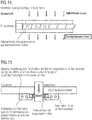
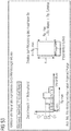
- FIG Figure 1 shows a method known from [7] for generating a depth profile.
- an ion beam is implanted into a substrate through a structured energy filter in a system for ion implantation for the purpose of wafer processing.
- the implantation method and the dopant distribution or defect distribution resulting from the implantation in the wafer after processing are shown. It is shown in particular how a monoenergetic ion beam is modified in its energy as it passes through a microstructured energy filter component, depending on the entry point.
- the resulting energy distribution of the ions leads to a modification of the depth profile of the implanted substance in the substrate matrix. This depth profile, which is rectangular in the example shown, is shown in FIG Figure 1 also shown.
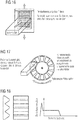
- Figure 2 shows a system for ion implantation.
- This system comprises an implantation chamber (implantation chamber) in which several wafers can be arranged on a wafer wheel.
- the wafer wheel rotates during implantation so that the individual wafers repeatedly pass through a beam opening in which the energy filter is arranged and through which the ion beam enters the implantation chamber and thus into the wafer.
- Links in Figure 2 shows the wafer wheel on which the substrates to be implanted are fixed.
- the wheel is tilted by 90 ° and set in rotation.
- the wheel is "written" with ions in concentric circles by the ion beam indicated in green.
- the wheel is moved vertically during processing.
- an energy filter is shown mounted in the beam opening.
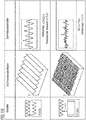
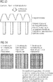
- Figure 3 shows exemplary layouts or three-dimensional structures of filters in order to illustrate in principle how a large number of different dopant depth profiles can be generated by a suitable choice of the filter.
- the individual, in Figure 3 The filter profiles shown can be combined with one another in order to obtain additional filter profiles and thus doping depth profiles. Shown are cross-sections of the energy filter (on the far left in the figures), top views of the energy filters and curves of the doping concentration achieved over the depth (as a function of the depth) of the wafer.
- the "depth" of the wafer is a direction perpendicular to the surface of the wafer in which to implant.
- (a) triangular prismatic structures cause a rectangular doping profile
- (b) smaller triangular prismatic structures a less deep-reaching rectangular doping profile compared to case (a) (the depth of the profile can therefore be adjusted via the size of the structures)
- (c) trapezoidal prismatic structures a rectangular doping profile with a peak at the start of the profile
- (d) pyramid-shaped structures a triangular doping profile increasing into the depth of the substrate.
- Previously known energy filters (implantation filters) or energy filter elements are not suitable for various reasons in order to achieve high throughputs, i.e. many wafers per hour. In particular, it is desirable to have high wafer throughputs per hour, easy handling, simple production and the realization of any profile shapes.
- Static or movably mounted filters are known from the literature, which are monolithic, ie made from a block of material and individually mounted to the ion beam [2], [3], [4], [5], [6], [7], [8], [9], [10].
- doped areas in SiC wafers can i.a. their shape cannot be changed by outdiffusion of doping profiles [2], [4], [5], [6].
- Doping depth profiles in semiconductor wafers can be produced by in-situ doping during the epitaxial deposition or by (masked) monoenergetic ion implantation.
- in-situ doping high inaccuracies can occur.
- homogeneous doping profiles are process-related on the wafer, ie from center to edge Deviations from the target allocation are to be expected.
- this inaccuracy also extends to the vertical direction of the doping area, since the local dopant concentration now depends on a large number of process parameters such as temperature, local doping gas concentration, topology, width of the Prandtl boundary layer, growth rate, etc.
- the use of monoenergetic ion beams means that many individual implantations have to be carried out in order to obtain doping profiles with acceptable vertical undulations. This approach is only scalable to a limited extent and quickly becomes economically unprofitable.
- Examples of the invention relate to the design of an energy filter element for ion implantation systems, so that this corresponds to the requirements resulting from the use of the energy filter element in the industrial production of semiconductor components, in particular for components based on SiC semiconductor material.
- production conditions are defined, for example, by the following aspects:
- the energy filter is a highly fragile, microstructured membrane that is difficult to handle without destroying it.
- Production conditions mean, for example, that ion implanters (typical terminal voltage at tandem accelerators> 1MV to 6MV) per hour should produce more than typically 20-30 wafers with a diameter of 6 "and area doses per wafer of approx
- ion currents of more than 1p ⁇ A up to a few 10p ⁇ A must be used, or outputs of more than a few watts, e.g. 6W / cm-2, are deposited on the filter (typical area 1-2cm 2 ). This leads to the heating of the filter and the task is to cool the filter by means of suitable measures.
- Filter structures can be produced by means of anisotropic wet chemical etching.
- the filter structures consist of suitably dimensioned triangular long lamellae (e.g. 6 ⁇ m high, 8.4 ⁇ m spacing, length a few millimeters), which are periodically arranged on a membrane that is as thin as possible.
- triangular lamellae e.g. 6 ⁇ m high, 8.4 ⁇ m spacing, length a few millimeters
- pointed triangular lamellae is cost-intensive, since the wet-chemical anisotropic etching must be precisely set.
- Pointed, i.e. non-trapezoidal lamellae are complex, as the etching rates and times must be precisely matched to one another for pointed lamellae.
- the energy filters for ion implantation described in the mentioned publications [2], [3], [4], [5], [6], [7], [8], [9], [10] have an internal 3-dimensional Structure that leads to differences in the path length of the ions when transmitted through the filter. These path length differences produce, depending on the braking capacity of the filter material, a modification of the kinetic energy of the transmitted ions. A monoenergetic ion beam is thus converted into a beam of ions with different kinetic energies. The energy distribution is determined by the geometry and the materials of the filter, ie the filter structure is transferred into the substrate by means of ion lithography.
- the total number of wafers processed with a specific filter should be monitored.
- the angular spectrum of the transmitted ions must be limited in order to avoid "under-implantation" of the masking layer.
- Electrons of the primary beam can be emitted or absorbed in the solid, ie the transmitted ions depend on the properties of the filter material and the primary energy after passing through the filter a higher or lower state of charge on average [26]. This can lead to positive or negative charging of the filter.
- the ion bombardment can generate secondary electrons with high kinetic energy both on the front and on the back of the filter.
- the energy filter will heat up, see Fig. 6.5.24. Due to thermionic electron emission (Richardson-Dushman law), thermal electrons are generated depending on the temperature and the work function of the filter material.
- the distance (in a high vacuum) of the ion accelerator between the filter and the substrate is typically only a few centimeters or less. This means that the diffusion of thermal electrons (from thermionic emission) and the action of fast electrons (from ion bombardment) falsify the measurement of the ion current on the substrate, for example by a Faraday cup attached there.
- microtechnical processes are proposed for the production of the energy filter.
- lithography processes in combination with wet-chemical or dry-chemical etching processes are used to produce the filters.
- the anisotropic wet chemical etching process using alkaline etching media (e.g. KOH or TMAH) in silicon is preferred for filter production.
- the functional filter layer is manufactured from monocrystalline silicon.
- An irradiation arrangement is to be used which allows a static substrate to be irradiated over the entire substrate surface in an energy-filtered manner with high lateral homogeneity.
- Partially mechanical scanners are also used, ie the beam is expanded in the x direction and the wafer is mechanically (slowly) moved in the y direction.
- An irradiation arrangement must be used which allows a static or movable substrate to be irradiated with energy filtering with a high degree of lateral homogeneity over the entire substrate area and thereby using a large filter area. This can reduce thermal effects and degradation effects in the filter.
- the energy filter is a tool for manipulating the doping profile in the substrate.
- a manipulation of the doping profile that can be generated in the substrate AFTER the energy filter is desirable.
- Such a doping profile manipulation after the energy filter can take place by implantation in a sacrificial layer on the substrate.
- a laterally variable doping profile in the substrate is desirable for certain applications.
- changing the implantation depth of a homogeneous doping profile for edge terminations in semiconductor components could be used advantageously.
- Such a lateral setting of the doping profile can take place on the substrate by means of a sacrificial layer that is laterally variable in its thickness.
- a multifilter is attached to the movable part of a movable substrate chamber, which moves in front of the beam with a linear pendulum movement (e.g. in the case of a rotating wafer disk with a vertical scanning device), a movement of the multifilter relative to the beam can easily be achieved through the Movement of the substrate chamber can be achieved.
- a magnetic or static scanning device in front of the filter in one direction, a very large multifilter surface can then be used, which results, for example, as the product of the vertical pendulum distance and the horizontal scanning distance.
- the movement of wafer and filter are coupled in this arrangement, which can lead to problems with regard to the lateral doping homogeneity. As the wafer wheel rotates, the ion beam "writes" lines on the wafers.
- the position of a horizontal irradiated line, for example, on the wafer is coupled to a specific vertical position on the multifilter.
- a gap between individual filter elements would, for example, result in an inhomogeneously doped line on the wafer.
- An arrangement of the filter components in the multifilter must therefore be selected so that the lateral homogeneity is guaranteed despite the coupling of the linear movements of the filter and the substrate.
- the filter chip which allows easy handling of the filter chip. to be built in.
- This framework can, as in the Figures 4 to 6 is shown, be designed in such a way that it can be used on the ion implantation system in a suitable frame holder preinstalled there.
- the frame protects the energy filter, allows easy handling and provides electrical and thermal dissipation or electrical insulation (see Figure 36 ).
- the frame can be supplied by the manufacturer of the filter elements with the filter chip assembled in a dust-free environment and delivered to the ion implantation system in dust-free packaging.
- the filter held therein can have any surface structure that is selected in accordance with the desired doping profile to be achieved with it.
- the filter holder and / or the filter frame can be provided with a coating that prevents material from being removed from the filter frame and filter holder.
- the filter frame and filter holder can be made of metals, preferably stainless steel, or the like.
- metals preferably stainless steel, or the like.
- sputtering effects in the local area of the energy filter must be expected, i.e. the frame and filter holder material must be expected to be removed from the surface.
- Metal contamination on the substrate wafer could be the undesirable consequence.
- the coating prevents such contamination, the coating being made of a non-contaminating material. Which substances are non-contaminating depends on the properties of the target substrate used. Examples of suitable materials include silicon or silicon carbide.
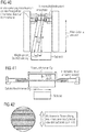
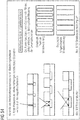
- FIG. 4 shows a cross section of a filter frame for receiving an energy filter chip.
- the energy filter chip that is in Figure 4 is also shown, can be fastened in various ways in the frame, such as by gluing by means of a vacuum-tight, temperature-stable and highly thermally conductive adhesive or by a mechanical spring.
- FIG. 5 shows a plan view of a filter frame for receiving an energy filter element which is shown in FIG Figure 5 is also shown.
- the filter frame has a closure element by means of which the frame can be opened and closed to change the energy filter.
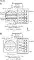
- Figure 6 illustrates an example of an installation of a frame for receiving an energy filter element in the beam path of an ion implanter. Is shown in the upper part of Figure 6 a cross section through the chamber wall and the filter holder arranged on it.
- the filter holder is arranged on the inside of the chamber wall, that is to say the side that faces the wafer (not shown) during implantation.
- the ion beam passing through the opening in the chamber wall and the filter arranged in front of the opening during implantation is in Figure 6 also shown schematically.
- the frame with the filter chip inserted into the filter holder covers the opening in the chamber wall, through which the ion beam passes during implantation. This is in the lower part of the Figure 6 which shows a top view of the chamber wall with the filter holder attached.
- the frame can be made of the same material as the filter.
- the frame can be made monolithic with the filter and can be called a monolithic frame.
- the frame can also consist of a different material than the filter, such as a metal.
- the filter can be inserted into the frame.
- the frame comprises a monolithic frame and at least one further frame made of a different material than the filter, which is attached to the monolithic frame.
- This further frame is, for example, a metal frame.
- the frame can completely surround the filter, as explained and shown above and as shown on the right in FIG Figure 7 is shown. According to further examples, the frame does not adjoin all (four) sides (edges) of the filter, but only adjoins three, two (opposite) or only one of the edges of the filter.
- a frame is understood to mean a full frame that completely surrounds the filter on the sides (edges), but also a sub-frame that only partially surrounds the filter on the sides. Examples of such sub-frames are in Figure 7 also shown. Figure 7 shows different sub-frames (left in the figure) and a full frame (far right in the figure). These frames can each consist of the same (eg monolithic) and / or a different material than the energy filter.
- the energy filter or any other scattering element can be fastened in various ways in the beam path of the implanter by means of its frame, which can be implemented according to one of the examples explained above.
- the above-mentioned pushing the frame into a filter holder is only one of several possibilities. Further possibilities are explained below.
- the frame can be attached to the chamber wall by at least one web.
- the at least one web serves as a filter holder.
- fastenings with only one bar, with two bars and with three bars. Of course, more than three webs can also be provided.
- the frame can also be attached to the chamber wall by suspensions or suspension elements.
- suspensions or suspension elements are, for example, flexible and can be stretched between the frame and the chamber wall in such a way that the frame is held firmly.
- the suspension elements act as a filter holder in this example.
- Figure 9 Examples of fixings with only one suspension, with two suspensions and with three suspensions. Of course, more than three suspensions can be provided.
- the frame with the filter is held floating (contactless) by magnets.
- magnets are attached to a front and a rear side of the frame and the chamber wall in such a way that a magnet on the chamber wall or a holder attached to the chamber wall is opposite a magnet on the frame, with opposite poles of the opposite magnets facing each other. Due to the magnetic forces, the frame is held in a floating manner between the magnets attached to the chamber wall or the holder.
- the magnets on the frame of the filter can be realized, for example, by thermal vapor deposition or any other layer-applying method.
- any desired doping profile in a semiconductor material can be achieved through the geometric configuration of an energy filter for ion implantation systems.
- any profiles can be generated with simple triangular structures (multifilter). If necessary, non-triangular structures (eg pyramids) can also be used as basic elements for approximation.
- multifilter simple triangular structures
- non-triangular structures eg pyramids
- the decomposition of a doping depth profile is not limited to the triangular structures shown here, but other structures, which in the most general case contain inclines or also convex or concave rising flanks.
- the flanks do not necessarily have to rise monotonically, but can also contain valleys and depressions. Binary structures with flank angles of 90 ° are also conceivable.
- the filter elements are cut out "at an angle" and placed directly next to one another.
- the angled cutting has the advantage that no adhesive bond is required between the filters to block ions at the edge of the filter.
- the irradiated area can be used optimally in this way. With the same overall filter dimensions and given ion current, this increases the wafer throughput.
- FIG. 11 illustrates an example of a simple implementation of a multifilter.
- three differently shaped filter elements are combined in a frame of the filter holder to form a whole energy filter.
- Top left is in Figure 11 a cross section through the filter holder with the three filter elements is shown and at the bottom left in FIG Figure 11 a top view of the filter holder with the three filter elements is shown.
- On the right in FIG. 11 there is shown a filter profile that can be achieved with the combined filter.
- the ion beam evenly sweeps over all the individual filter elements, so that the right in Figure 11 shown dopant depth profile is achieved.
- This profile contains three sub-profiles numbered 1, 2 and 3. Each of these sub-profiles results from one of the three sub-filters shown on the left, namely from the sub-filter provided with the corresponding number.
- Figure 12 illustrates an example of the functionality of three different filter elements that can be combined to form a multifilter.
- Figure illustrates a cross section through the individual filter elements, exemplary dimensions of these filter elements and dopant profiles, as achieved by the individual filter elements can be.
- a fourth filter element not shown, in Figure 12 only exemplary dimensions given.
- the weighting ie the resulting concentration or the doping profile, can be adjusted by dimensioning the surfaces of the individual filter elements.
- the filter and the substrate have the same energy-dependent braking capacity, but this does not have to be the case.
- FIG. 10 shows an example of a doping profile that can be obtained when the four are based on FIG Figure 12 explained filter elements can be combined into a multifilter and used for implantation.
- Figure 14 shows a cross section through a multifilter which has several adjoining filter elements F1, F2, F3 and which is inserted into a filter frame.
- the individual filter elements F1, F2, F3 are sawed at an angle in the example and arranged directly adjacent to one another.
- Such cooling can be achieved, for example, by one or more of the following under a. to c. explained measures take place:
- FIG 15 shows an example of such a cooled filter holder.
- a cross section is shown a filter holder that is attached to a chamber wall of an implanter.
- cooling lines are integrated in the filter holder, which receives the filter frame, and are supplied with cooling liquid by an external cooling device (not shown).
- the cooling lines can also be arranged on the surface of the filter holder (not shown).
- the filter or the holder of the filter When using a rotating wafer wheel loaded, for example, with 10-15 wafers, it is proposed to design the filter or the holder of the filter in such a way that it rotates or oscillates with a linear movement.
- the ion beam can be moved electrostatically over the filter when the filter is stationary.
- the filter is only partially irradiated by the ion beam per unit of time. This means that the part of the filter that is currently not being irradiated can be cooled by radiation. In this way, averaged higher current densities can be achieved with a given filter in continuous use. Examples of how this can be achieved are in the Figures 16 and 17 shown.
- Figure 17 illustrates an energy filter with a relatively large area, which is only partially irradiated per unit of time. In this way, the non-irradiated areas can cool down using radiation cooling.
- This embodiment can also be designed as a multifilter, as described above. That is, as a filter that has several different filter elements.
- the frame with the filter oscillates in a direction perpendicular to the beam direction of the ion beam, which is shown schematically.
- the area of the filter covered by the ion beam is less than the total area of the filter, so that only part of the filter is irradiated per unit of time. This part changes constantly due to the pendulum movement.
- Figure 11 shows an example of a filter assembly with multiple filter elements held by a rotating filter holder.
- the individual filter elements can each have the same structure, but can also be structured differently in order to obtain a multifilter.
- Figure 18 when the holder rotates, the individual filter elements move on a circular path around the axis of rotation (central axis) of the holder.
- FIG. 18 An example of such a filter is in Figure 18 shown.
- a cross section (left in the figure), a top view (in the middle) and an example of a doping profile that can be achieved by the filter shown are shown.
- a rectangular profile can be generated in the substrate by implanting ions into the energy filter with the aid of a trapezoidal prismatic structure.
- the initial peak is implanted in the energy filter, ie there is no doping profile peak within the substrate.
- the implantation profile has the advantageous property that it begins directly at the substrate surface, which can be of decisive importance for the application of the energy filter.
- this filter structure has plateaus instead of spikes, the individual structural elements are therefore trapezoidal in cross-section. This considerably simplifies the process-related implementation of the filter. It is known to produce triangular structures in silicon, for example by wet chemical etching using KOH or TMAH. For this, the lithographic covering of the triangle tips is necessary. If perfect tips are to be produced, this leads to the problem of undercutting of the lacquer or hard mask structure. Without the idea proposed here, this problem can only be solved by perfect (and thus complex, cost-intensive) processing. The idea proposed here thus simplifies the production of the Filter structures are very important. This also applies analogously to modern plasma-assisted etching processes such as RIBE or CAIBE.
- the aspect of lateral homogeneity can be essential in static implantation situations.
- the homogeneity is determined by the rotational and translational movement of the wafer disk relative to the ion beam.
- Filter-substrate distance The angular distribution of the transmitted ions depends on the energy. If the filter and the energy of the ions are matched to one another in such a way that, among other things, very low-energy ions (nuclear braking regime) leave the filter, the width of the angular distribution is large, since large-angle scattering events often occur. If the filter and the energy of the ions are matched to one another in such a way that only high-energy ions (only in the electronic regime, dE / dx electron > dE / dx nuclear ) leave the filter, the angular distribution is very narrow.
- a minimum distance is characterized by the fact that the structure of the filter is not transferred into the substrate, i.e., for example, that with a given scattering angle distribution of the transmitted ions, they cover at least a lateral distance comparable to the period of the lattice constant of the ion filter.
- a maximum distance is determined by the loss that is still to be tolerated by the application (semiconductor component) for a given scattering angle distribution due to scattered ions, in particular at the edge of the semiconductor wafer.
- Figure 19 This shows the result of an experiment in which ions were implanted through an energy filter during static implantation into a PMMA (polymethyl acrylate) substrate.
- the ions destroy the molecular structure of the PMMA, so that a subsequent development process reveals the energy distribution of the ions in such a way that areas of high energy deposition are dissolved. Areas with little or no energy deposition by ions are not dissolved in the developer solution.
- the idea proposed here is to generate a high lateral doping homogeneity for both dynamic and static implantation arrangements with the correct choice of the filter-substrate distance.
- the filter is changed in its chemical composition, its density and its geometry in such a way that the effects on the target profile to be realized can no longer be neglected.
- a specification can therefore be defined which includes a maximum temperature during implantation and a maximum permitted accumulated ion dose.
- the use of the energy filter is monitored in such a way that it cannot be used outside of the specification, even without monitoring by an engineer.
- each filter be recorded with an electronically readable signature as soon as the filter is inserted into the filter holder on the implanter and that this signature be read out, for example by a control computer.
- the signature is stored, for example, in an electronically readable memory arranged on the filter.
- the signatures of the filters that can be used on a certain implanter and their properties are stored, such as for which process (ion type, energy) the filter is suitable and which accumulated dose and which maximum temperature may be reached.
- the control computer can thus determine whether the filter is suitable for a planned implantation process.
- Figure 20 illustrates a control system for identifying the filter and for monitoring compliance with the filter specification (maximum temperature, maximum accumulated ion dose). If the filter is identified by the built-in sensors (charge integrator and temperature sensor), for example, the accumulated ion dose and the temperature of the filter are continuously measured. The implantation process is ended when one of the specified parameters is reached or exceeded, for example when the filter becomes too hot or the maximum permitted dose has been implanted through the filter. In other words, if the specification is violated, a signal is sent to the control computer, which ends the implantation process.
- the filter specification maximum temperature, maximum accumulated ion dose
- a mask can be applied to the target substrate.
- collimate the ion beam transmitted through the filter In order to avoid a lateral "softening" of the structures due to a filter-induced excessively wide ion distribution, it is proposed to collimate the ion beam transmitted through the filter.
- the collimation can take place by means of stripes, tubes, grids or hexagonal structures with high aspect ratios, which are placed in the transmitted beam after the energy filter.
- the aspect ratio of these structures defines the maximum permitted angle.
- Figure 21 shows a cross section of an implanter chamber wall in the area of the jet opening, a filter holder attached to the chamber wall with an inserted filter and a collimator, which in the example is attached to a side of the filter holder facing away from the chamber wall.
- An aspect ratio of the collimator which is determined by the length and the width of the collimator, determines the maximum angle ⁇ relative to the longitudinal direction of the collimator at which the ion beam can be radiated into the collimator in order to pass the collimator. Portions of the ion beam that are radiated at larger angles end on the wall of the collimator, i.e. do not pass through it.
- the collimator can also consist of several collimator units with a smaller opening arranged next to one another. These can, for example, be arranged in a honeycomb shape.
- the collimator structure can also be arranged directly on the filter element.
- Such an element can be produced monolithically or by microbonding processes.
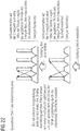
- Two examples of such a collimator structure arranged directly on the filter are shown in FIG Figure 22 shown.
- Such a collimator structure arranged directly on the filter can mechanically stabilize the filter and also have a cooling effect, since the collimator structure can act as a heat sink with a larger surface compared to the filter.
- the maximum angle ⁇ is also defined here by the aspect ratio of the individual collimator structures arranged on the filter, each of which has a length and a width.
- the collimator structure can be attached to the filter, for example by gluing, bonding, or the like.
- the collimator structure is arranged on the structured side of the filter, that is, where the filter has elevations and depressions.
- the structures are trapezoidal.
- FIG. 13 shows a modification of the arrangement of FIG Figure 22 .
- the collimator structure is arranged on the unstructured side of the filter. In both cases, the collimator structure is in the beam direction of the ion beam (the one in the Figures 21 and 22nd is symbolized by the arrow) after the filter, so that the ion beam passes the collimator structure after passing through the filter.
- Figure 24 shows top views of collimator structures according to various examples.
- this collimator structure is arranged on a filter which, in plan view, has a lamellar structure.
- the individual "filter lamellas" can, for example, be triangular or trapezoidal in cross section, as explained above.
- a lamellar structure of the filter is only one example. Any other filter structures as explained above can also be used.
- In the left part and in the middle shows Figure 24 one example each in which the collimator structure is strip-shaped, that is to say has a plurality of parallel strips which each extend over the entire width of the filter.
- a collimator is formed by two adjacent strips, the width of this collimator being determined by the distance between the adjacent strips.
- the length of the collimator is determined by the height of the individual strips.
- the "height" of the strips is their dimension in a direction perpendicular to the plane of the drawing.
- the strips of the collimator structure can run perpendicular to the lamellae of the filter, as shown on the left in FIG Figure 24 is shown, or can run parallel to the slats, as shown in the middle.
- Right is in Figure 24 an example is shown in which the collimator structure in plan view is lattice-shaped, whereby a plurality of collimators are formed, whose geometry is determined by the geometry of the grid.
- the individual collimators are rectangular in plan view, in particular square, so that the collimators are rectangular tubes.
- the grid can also be implemented in such a way that the individual collimators are circular, elliptical or hexagonal (honeycomb-shaped) or have any other polygonal geometry when viewed from above.
- a masking acting as a collimator structure can be applied to the target wafer.
- One condition for this masking can be that the braking capacity of the masking must at least correspond to the mean range of the transmitted ion beam in the target substrate material.
- the aspect ratio of the masking can be adapted accordingly.
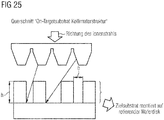
- Figure 25 Figure 3 shows an example of such a collimator structure placed directly on the target substrate.
- This collimator structure can have any of the geometries explained above, that is to say, for example, lamellar, strip-shaped, tubular or honeycomb-shaped - depending on the layout of the substrate structure and the required maximum angular distribution.
- the aspect ratio of this collimator structure is the ratio of height (h in Figure 25 ) to width (b in Figure 25 ) the recesses of the mask forming the collimator structure on the substrate.
- the collimator structure not only influences the scattering in the lateral direction, but also the depth profile.
- Figure 26 shows the doping profiles for three different implantation procedures, each performed with the same filter but different collimator structures.
- the filter has a lamellar structure with a trapezoidal cross section. But this is just an example.
- an implantation method is illustrated in which implantation is carried out without a collimator structure. The implantation profile thus obtained begins on the surface of the substrate.
- the doping profiles obtained by this implantation method do not start at the surface of the substrate but rather spaced apart from it, the doping profiles being spaced further apart from the surface and increasing the flatter the greater the aspect ratio. This can be explained by the fact that the dopant profile in the area of the substrate close to the surface is caused by ions that are more strongly decelerated in the filter and therefore have a lower energy.
- Such ions with low energy are more strongly scattered by the filter than ions with higher energy, so that these ions with lower energy have a larger angular distribution than ions with higher energy.
- more ions with lower energy than ions with higher energy no longer pass through the collimator structure, this effect being more pronounced the greater the aspect ratio of the collimator structure, i.e. the smaller the maximum angle at which the ions can still pass the collimator structure be able.
- the filter can be designed in such a way that ions with low energy are "preferred", that is, more ions with lower energy than ions with higher energy pass the filter.
- An example of such a filter is in Figure 27 shown.
- the filter has different filter areas, each of which has a maximum and a minimum thickness. The maximum thickness is the same in all three areas, but the minimum thickness is different. This is achieved in the example in that the filter in each of the individual areas has a trapezoidal structure arranged on a base area, the height of the base being of different thicknesses or the trapezoidal structures being of different heights.
- the thickness of the base is smallest and the trapezoidal structure is highest, as a result of which a distance CD1 between adjacent structures is greatest in this section.
- the thickness of the base is greatest and the trapezoidal structure is the smallest, as a result of which a distance CD3 between adjacent structures in this section is the smallest.
- the thickness of the base is between the thickness in the first section and the thickness in the third section, correspondingly a height of the trapezoidal structure in this section is between the height in the first section and in the third section and a distance CD2 between adjacent structures in this section between the distance CD1 in the first section and the distance CD3 in the third section.
- the individual sections can be the same size in relation to their area but also be of different sizes. In addition, more than three sections with different minimum filter thicknesses can of course also be provided.
- Figure 27 shows, in the left part, an implantation profile that is obtained with implantation with the filter described, when implantation is carried out without a collimator structure.
- This implantation profile begins on the surface, but the doping concentration decreases in steps with increasing depth.
- CD1 denotes a region of the doping profile produced by the first section of the filter
- CD2 denotes a region of the doping profile produced by the second section of the filter
- CD3 denotes a region of the doping profile produced by the third section of the filter.
- the doping profile shows that the ions passing through the respective filter area penetrate less deeply into the substrate, that is to say that their energy is lower, the greater the minimum thickness of the base of the respective section.
- the doping profile shows that more ions with low energy pass through this filter than ions with high energy.
- the ions with lower energy are more strongly scattered than the ions with higher energy, and thus fewer ions with lower energy than ions with higher pass a collimator structure, when using such a filter in conjunction with a collimator structure an approximately homogeneous doping profile beginning at the surface can be achieved.
- FIG. 27 shows that an implantation method using the explained filter and a collimator structure is shown.
- the collimator structure is located on the substrate, but can also be arranged on the filter.
- Implantation arrangement of the filter to the substrate, one point towards the substrate, once point away from the substrate ⁇ sputtering, scattering on impact.
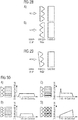
- the filter can be used in such a way that the microstructures of the filter face the substrate, that is, point away from the ion beam, as in FIG Figure 28 (a) is shown.
- the filter can also be rotated so that the microstructures of the filter are facing away from the substrate, i.e. point towards the ion beam, as in FIG Figure 28 (b) is shown.
- the latter can have advantageous effects on sputtering effects in the filter.
- the filter and / or substrate are made of crystalline material, undesirable channeling effects can occur. This means that ions can achieve an increased range along certain crystal directions.
- the size of the effect and the acceptance angle are temperature and energy dependent.
- the implantation angle and the crystallographic surface orientation of the raw material used for the filter and substrate play a decisive role. In general, the channeling effect cannot be reliably reproduced over a wafer, since the above parameters can differ from wafer to wafer and from implantation system to implantation system.
- Channeling should therefore be avoided. Tilting the filter and substrate can prevent channeling. Channeling in the filter or in the substrate can have very different effects on the depth profile of the implanted dopant, especially if the filter and substrate are made of different materials.
- Figure 29 shows schematically a filter which is tilted relative to the substrate during the implantation process in such a way that a base area of the filter encloses an angle with a surface of the substrate which is greater than zero. This angle is, for example, greater than 3 °, greater than 5 ° or greater than 10 ° and smaller than 30 °.
- a channeling effect can be prevented or reduced as a result.
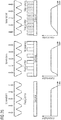
- Figure 30 shows a schematic representation of various doping profiles (doping concentration as a function of the depth in the substrate) for differently shaped energy filters, each of which is shown in a side view and a top view.
- triangular prismatic structures produce a rectangular doping profile
- smaller triangular prismatic structures produce a less depth-distributed doping profile than the larger triangular prismatic ones shown in (a) Structures
- trapezoidal prismatic structures produce a rectangular doping profile with a peak at the start of the profile
- pyramidal structures produce a triangular doping profile that rises into the depth of the substrate.
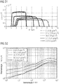
- Figure 32 illustrates the course of the braking capacity as a function of the energy [4] (SRIM simulation) for the various substrate materials that are shown in the illustration in Figure 31 underlie.
- Figure 33 Fig. 10 illustrates a multilayer starting material for a multilayer filter.
- this starting material comprises four different layers, which are labeled 1 to 4.
- the use of four layers is just one example. Less than or more than four different layers can also be used.
- the individual layers can differ not only in terms of the material used but also in terms of their thickness. It is also possible for two layers to have the same material and to be separated by two or more layers of different materials.
- the individual layers can be deposited or produced sequentially on top of one another by suitable deposition processes.
- FIG. 13 shows a cross section of a filter based on the in FIG Figure 33 produced starting material was realized and which in the example shown has a base and triangular structures arranged on the base. These triangular structures can be strip-shaped, that is to say elongated in a direction perpendicular to the plane of the drawing, or they can also be part of pyramidal structures.
- the filter can also be implemented in such a way that several structures are arranged next to one another in the lateral direction (y-direction), which have different geometries and / or different layer stacks, ie layer stacks with different structures with regard to the sequence of individual layers and / or the material of the individual layers.
- y-direction lateral direction
- the filter shown six different materials are used in the filter shown, which are labeled 1-6.
- Suitable materials for the individual layers are, for example, without being restricted to such materials, silicon, silicon compounds or metals.
- Silicon compounds are, for example, silicon carbide (SiC), silicon oxide (SiO 2 ) or silicon nitride (SiN).
- Suitable metals are, for example, copper, gold, platinum, nickel or aluminum.
- at least one layer made of a silicon compound is grown on a silicon layer and on the at least one layer made of a silicon compound a metal layer is vapor-deposited.
- a metal layer can also be vapor-deposited directly onto a silicon layer. It is also possible to produce different metal layers on top of one another by vapor deposition in order to obtain different layers of the filter.
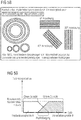
- Figure 36 illustrates the equilibrium charge states of an ion (black line: Thomas-Fermi estimate, blue line: Monte Carlo simulations, red line: experimental results) as a function of the kinetic energy of the ion when irradiating a thin membrane.
- Ion sulfur
- membrane carbon.
- the ion bombardment can generate secondary electrons with high kinetic energy both on the front and on the back of the filter.
- the energy filter will heat up. Due to thermionic electron emission (Richardson-Dushman law), thermal electrons are generated depending on the temperature and the work function of the filter material.
- Figure 37 shows the heating of an energy filter by ion bombardment. The curve shown is based on an experiment in which a filter was irradiated with carbon (C) ions with an energy of 6 MeV. The filter in this case was a non-transparent energy filter [2].
- the distance (in a high vacuum) of the ion accelerator between the filter and the substrate is typically only a few centimeters or less. This means that the diffusion of thermal electrons (from thermionic emission) and the action of fast electrons (from ion bombardment) falsify the measurement of the ion current on the substrate, for example by a Faraday cup attached there.
- the filter As described, from the perspective of the filter there are processes that deliver electrons (stripping of the primary ions) and there are processes that emit electrons. So the potential is one
- the electrically insulated filter is not well defined, but will vary depending on the ion current, vacuum conditions, temperature, etc. during the implantation process. A net negative charge will encourage the emission of electrons, a net positive charge will tend to suppress the emission of electrons. Various ways of preventing such charging are explained below.
- Figure shows a cross section of a filter arrangement in which this is ensured.
- the filter in the filter frame is held at a defined (positive) potential with respect to the filter holder for the purpose of suppressing secondary electrons.
- the filter frame is connected to a voltage source and is electrically isolated from the filter holder and the chamber wall of the implanter.
- the electrical potential of the filter holder can be regulated. For example, in such a way that, regardless of the charge balance resulting from the implantation process, a constant potential is set during the implantation with respect to the potential of the substrates to be implanted or the earth potential. For this purpose, a regulated supply of positive or negative charge can take place from a power source.
- the potential to be set can in particular be selected so that, for example, the emission of electrons from the filter is completely suppressed and thus only the (positive) charge of the transmitted ion current is measured in the Faraday cup next to or on the substrate.
- Typical values for such a (positive) potential are between a few 10V and a few 1000V.
- the energy filter has a very high resistance due to its material nature
- the stopping power of this layer must be included in the overall balance of the stopping power when designing the filter. Care must be taken that the applied layer (even when applied on the side facing away from the substrate) does not in principle cause any harmful effects Contamination caused in the substrate material to be implanted.
- the layer can consist of carbon, for example.
- the stopping power of this layer should be included in the overall balance of the stopping power when designing the filter. It must be ensured that the applied layer (even when applied on the side facing away from the substrate) does not in principle cause any harmful contamination in the substrate material to be implanted.
- Ad 12 Alternative manufacturing methods using injection molding, casting or sintering processes
- Another advantage is that the use of the above-mentioned molding processes can greatly reduce the costs of producing a large number of filter elements compared to microtechnical production.
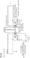
- Figure 40 shows an arrangement for implantation in a substrate through an energy filter. This arrangement comprises a deflection device for the ion beam, which is arranged in front of the filter.
- the deflection of the ion beam which can be achieved by this deflection device, is matched to the distance between filter and substrate (typically in the range from a few cm to a few m) that the substrate is irradiated completely, ie over its entire surface, for the purpose of implantation can be.
- Ad 14 Arrangement for utilizing a large filter area
- Figure 41 illustrates an arrangement for an energy filter implantation (i.e. an implantation by means of an energy filter) in which the beam area has been enlarged by suitable measures and the irradiated filter area is larger than the substrate area, whereby a complete irradiation of the substrate can be achieved and a large filter area can be used can.
- the irradiated filter area diameter is larger than the substrate diameter.
- a minimum distance between the substrate and the filter should be maintained, which ensures that there is sufficient lateral homogenization of the implanted ions due to scattering effects.
- the same arrangement as described in FIG. 14 a) is initially used:
- the arrangement of an energy filter implantation in which the beam area has been enlarged by suitable measures and the irradiated filter area is larger than the substrate area.
- the filter consists of an arrangement of a number of, for example, strip-shaped filter elements. These filter elements can, for example, be produced monolithically from a substrate by suitable production processes.
- Figure 42 Fig. 10 illustrates a partially active filter with mechanical unidirectional scanning.
- Ad 15 Modification of the doping profile in the substrate by means of a sacrificial layer
- a sacrificial layer can be applied to the substrate, the thickness and stopping power of which is selected in a suitable manner, so that the depth of the implantation profile in the substrate is shifted in the desired manner.
- a sacrificial layer can be used for masked ion implantation (cf. Figure 43 ) or for unmasked ion implantation.
- this method allows an undesired beginning of a doping profile to be "pushed out" of the substrate into the sacrificial layer by implanting the beginning of the profile into the sacrificial layer.
- Figure 43 illustrates a modification of the doping profile in the substrate by means of a sacrificial layer in the case of a masked, energy-filtered implantation.
- the beginning of the implantation profile is pushed into the sacrificial layer.
- This principle can be used in an analogous manner for an unmasked, energy-filtered ion implantation, i.e. an implantation in which different than in Figure 43 shown there is no mask layer.
- Ad 16 Lateral modification of the doping profile in the substrate by means of a sacrificial layer
- a sacrificial layer is applied to the substrate, the stopping power and course of the thickness over the wafer surface being selected in a suitable manner so that the depth of the implantation profile in the substrate is shifted in the desired manner depending on the lateral position on the wafer.
- a sacrificial layer can be used for masked ion implantation or also for unmasked ion implantation (cf. Figure 44 ) be used.
- changing the implantation depth of a homogeneous doping profile for edge terminations in semiconductor components can be used advantageously.
- Figure 44 illustrates a lateral modification of the doping profile in the substrate by means of a sacrificial layer in the case of an unmasked, energy-filtered ion implantation.
- a lateral modification of the implantation depth comes about here due to a different thickness of the sacrificial layer in the lateral direction.
- the principle can be used analogously for masked, energy-filtered implantations.
- Ad 17 Adaptation of a profile transition of several implantation profiles
- Two or more doping profiles can be skilfully overlapped, so that a desired overall doping profile is created, in particular in the area of the overlap.
- This technique is particularly advantageous when growing and doping several layers.
- a representative example is the growth of several SiC epi layers and the respective energy-filtered doping. Good contact between the layers should be ensured here.
- Ad 18 Special arrangement of the multifilter concept with coupled pendulum movement
- a clever arrangement can be used so that, despite the coupled pendulum movement of filter and substrate, that is, no relative vertical movement between filter and substrate, a lateral homogeneity of the distribution of the ions is achieved.
- Such an arrangement is in Figure 45 shown.
- the wafers are guided along behind the substrate by the rotation of the wafer wheel in the x-direction.
- the ion beam (not shown) is expanded in the x direction, for example, and is scanned over the entire multifilter surface by the vertical pendulum movement of the implantation chamber.
- the surface consists of active filter areas and inactive support areas.
- Arrangement A) is an unfavorable arrangement.
- Arrangement A is a rather unfavorable arrangement. If one considers the irradiated filter area for y1 and y2, then at y1 3 filters are irradiated while at y2 no filter at all is irradiated. The result is a laterally inhomogeneous stripe pattern on the wafer.
- Arrangement B shows a possible example of a better arrangement. Two filters are irradiated for both y1 and y2. This is true for all y. This results in a laterally homogeneous doping over the wafer surface.
- Another aspect is to solve the task of monitoring important parameters of the ion implantation modified by an energy filter.
- Such parameters are, for example, the minimum or maximum projected range, the depth concentration distribution set by the filter geometry and the (energy-dependent) angle distribution.
- Monitoring other parameters such as implanted ion species, etc., could also be useful.
- Monitoring should be possible in particular on the wafers to be implanted or on structures (several in parallel) that are arranged in the vicinity of the wafers. According to one aspect, the monitoring should be carried out without further processing of the monitoring structures or the wafers.
- Monitoring can be carried out by measuring optical parameters such as spectral absorption, spectral transmission, spectral reflection, changes in the refractive index, global absorption (wavelength range depending on the measuring device) and global transmission, as well as reflection (wavelength range depending on the measuring device).
- optical parameters such as spectral absorption, spectral transmission, spectral reflection, changes in the refractive index, global absorption (wavelength range depending on the measuring device) and global transmission, as well as reflection (wavelength range depending on the measuring device).
- masks and substrate materials for monitoring the mentioned implantation parameters which (1) are arranged at a suitable place on the surface to be implanted, eg wafer wheel, and (2) their eg optical properties "as implanted" by ion implantation ", ie change it without further post-processing in such a way that, for example, the change is proportional to the implanted ion dose for a given type of ion.
- Such materials mentioned under (2) are, for example, PMMA (Plexiglas), PMMA, SiC, LiNbO3, KTiOPO4 or the like.
- the target substrate e.g. a SiC wafer
- the target substrate can be used directly for optical monitoring.
- Such changes can be, for example, mechanical properties of the monitor material, electrical properties of the monitor material or also the nuclear physical activation of the monitor material by high-energy ion radiation.
- the detection should take place via the change in optical properties.
- Such an implementation will be described below.
- a monitoring structure consists of the arrangement of a suitable substrate material with one or more mask structures. Examples are in the Figures 47 and 48 shown.
- the monitoring structure or structures are, as in Figure 46 shown at a suitable location, for example on the wafer wheel, arranged.
- the monitoring chips are read out after implantation, for example without further post-processing. Possibly. the mask for the readout measurement must be separated from the monitoring substrate. In one aspect, the mask is reusable.
- Mask material and substrate material of the monitoring chip can be made of different materials.
- the criteria for selecting the mask material are, for example, compatibility with the material of the target substrates (in order to exclude contamination by sputtering effects) and a braking capacity for high-energy ions such that mask structures with high aspect ratios can be produced.
- the mask material and the substrate material of the monitoring chip can be made from the same material.
- the mask and substrate can also be produced monolithically. In this case, it is usually not possible to reuse the mask or the substrate.
- the lateral dimensions of the individual structures can be, depending on the requirements of the readout apparatus, from square micrometers, through square millimeters to square centimeters.
- Figure 53 a structure is shown which is suitable for monitoring the maximum projected range.
- Analog structures using evaluation procedures as described under A., can also be used to measure or monitor the minimum projected range.
- the ion implantation energy filter is known to produce an energy dependent spectrum of ion angles after passing through the filter.
- the resulting angular distribution is therefore a function of the filter geometry, the change in the geometry during the service life of the filter, the occurrence of channeling effects, the type of ion used, the primary energy, the resulting maximum and minimum energy of the transmitted ions and the geometric arrangement in the implantation chamber. All of these parameters can be monitored by monitoring the angular distribution.
- the opening sizes of the mask structures for thin masks that are only slightly thicker than the maximum projected range in the mask material can therefore be in the micrometer or submicrometer range.
- Such monitoring structures are preferably arranged as arrays which consist of many individual structures in order to be able to carry out a global (ie on an area of several mm 2 or cm 2) optical evaluation.
- the opening sizes can be in the millimeter or centimeter range. In these cases, the evaluation of individual structures that are not arranged in an array is also possible without excessive technical effort.
- Circular arrangements are also conceivable.
- the core of the aspects explained last is to use the (essentially) dose-dependent modification of the (preferably) optical parameters of a material for the "as implanted" monitoring of the energy filter implantation process.
- the most important parameters of the resulting implantation result can be monitored as completely as possible by means of an (for example) optical measurement, without the need for complex post-processing (e.g. annealing and application of metallic contacts).
- Figure 59 illustrates an adaptation of a profile transition of two implantation profiles A and B in a skilful manner, so that the resulting overall concentration profile can, for example, generate a desired homogeneous profile.
- This can (but does not have to) be advantageous, especially in the case of layer systems consisting of 2 layers, as in the picture shown here.
- the options for designing the high-energy tail of implant A are limited, but the low-energy tail of implant B can be influenced in particular by introducing a sacrificial layer, as described in "15: Modifying the doping profile in the substrate using a sacrificial layer".
- Proposal for an implementation with the following process sequence 1) Growing up sacrificial layer. 2) doping the lower Layer (Implant B). 3) Remove the sacrificial layer. 4) Grow the top layer. 5) doping the top layer.
- the concepts explained above enable production-compatible implantation processes for the semiconductor industry, i.e. an economical application of implantation processes in an industrial production process.
- the concepts explained enable, in particular, a very flexible (multifilter concept) implementation of complex vertical doping concentration profiles with a low angular distribution of the implanted ions.
- all types of doping concentration profiles can be approximated by using triangular filter structures in conjunction with collimator structures.
- Another important aspect concerns the suppression of artifacts which falsify the ion current measurement on the substrate.
- Ad 1. to Ad 19. can each be used on their own, but also in any combination with one another.
- the explained “end-of-life” detection can be applied to a filter held by a frame, but can also be applied to a filter held otherwise.
- the wafer explained above can be a semiconductor wafer, but can also consist of another material to be implanted, such as PMMA, for example.
Description
Die Erfindung betrifft eine Implantationsanordnung mit einem Energiefilter (Implantationsfilter) für eine Ionenimplantation und dessen Verwendung und ein Implantationsverfahren.The invention relates to an implantation arrangement with an energy filter (implantation filter) for ion implantation and its use and an implantation method.
Mittels Ionenimplantation kann eine Dotierung bzw. die Erzeugung von Defektprofilen in beliebigen Materialien, wie etwa Halbleitern (Silizium, Siliziumcarbid, Galliumnitrid) oder optischen Materialien (LiNbO3), mit vordefinierten Tiefenprofilen im Tiefenbereich von wenigen Nanometern bis hin zu einigen 100 Mikrometern erreicht werden. Wünschenswert ist es dabei insbesondere Tiefenprofile zu erzeugen, die durch eine größere Tiefenverteilungsbreite charakterisiert sind als die Breite eines durch einen monoenergetischen Ionenstrahlung erzeugbaren Dotierkonzentrationspeaks oder Defektkonzentrationspeaks, oder Dotier- oder Defekttiefenprofile zu erzeugen, welche durch eine oder einige wenige einfache monoenergetische Implantationen nicht erzeugt werden können.Ion implantation can be used to dop or generate defect profiles in any materials, such as semiconductors (silicon, silicon carbide, gallium nitride) or optical materials (LiNbO3), with predefined depth profiles in the depth range from a few nanometers to a few 100 micrometers. It is particularly desirable to generate depth profiles that are characterized by a greater depth distribution than the width of a doping concentration peak or defect concentration peak that can be generated by monoenergetic ion radiation, or to generate doping or defect depth profiles that cannot be generated by one or a few simple monoenergetic implantations .
-
Figur 1 veranschaulicht das Grundprinzip eines Energiefilter: Ein monoenergetischer Ionenstrahl wird beim Durchtritt durch eine mikrostrukturierte Energiefilterkomponente abhängig vom Eintrittsort in seiner Energie modifiziert. Die resultierende Energieverteilung der Ionen führt zu einer Modifikation des Tiefenprofils des implantierten Stoffes in einer Substratmatrix.Figure 1 illustrates the basic principle of an energy filter: A monoenergetic ion beam is modified in its energy when passing through a micro-structured energy filter component, depending on the entry point. The resulting energy distribution of the ions leads to a modification of the depth profile of the implanted substance in a substrate matrix. -
Figur 2 zeigt links ein Waferrad auf welchem zu implantierende Substrate fixiert werden. Bei der Prozessierung/Implantation wird das Rad um 90° nach gekippt und in Rotation versetzt. Das Rad wird somit in konzentrischen Kreisen durch den in grün angedeuteten Ionenstrahl mit Ionen "beschrieben". Um die gesamte Waferfläche zu bestrahlen, wird das Rad während der Prozessierung vertikal bewegt. Rechts zeigtFigur 2 ein montiertes Energiefilter im Bereich des Strahlaustritts.Figure 2 shows on the left a wafer wheel on which substrates to be implanted are fixed. During processing / implantation, the wheel is tilted by 90 ° and set in rotation. The wheel is "written" with ions in concentric circles by the ion beam indicated in green. In order to irradiate the entire wafer surface, the wheel is moved vertically during processing. Right showsFigure 2 a mounted energy filter in the area of the beam exit. -
Figur 3 zeigt eine schematische Darstellung verschiedener Dotierprofile (Dotierkonzentration als Funktion der Tiefe im Substrat) für unterschiedlich geformte Energiefiltermikrostrukturen (jeweils in Seitenansicht und Aufsicht dargestellt). (a) Dreiecksprismenförmige Strukturen erzeugen ein rechteckförmiges Dotierprofil. (b) Kleinere dreiecksprismenförmige Strukturen erzeugen ein weniger tiefenverteiltes Dotierprofil. (c) Trapezprismenförmige Strukturen erzeugen ein rechteckförmiges Dotierprofil mit einem Peak am Profilbeginn. (d) Pyramidenförmige Strukturen erzeugen ein dreiecksförmiges, in die Tiefe des Substrates ansteigendes DotierprofilFigure 3 shows a schematic representation of different doping profiles (doping concentration as a function of the depth in the substrate) for differently shaped energy filter microstructures (each shown in side view and top view). (a) Triangular prismatic structures produce a rectangular doping profile. (b) Smaller triangular prismatic structures produce a less depth-distributed doping profile. (c) Trapezoidal prismatic structures generate a rectangular doping profile with a peak at the start of the profile. (d) Pyramid-shaped structures produce a triangular doping profile that increases into the depth of the substrate -
Figur 4 zeigt einen Querschnitt eines Filterrahmens zur Aufnahme eines EnergiefilterchipsFigure 4 shows a cross section of a filter frame for receiving an energy filter chip -
Figur 5 zeigt eine Draufsicht auf einen Filterrahmen zur Aufnahme eines Energiefilterelements mit Verschlusselement und montiertem EnergiefilterFigure 5 shows a plan view of a filter frame for receiving an energy filter element with a closure element and mounted energy filter -
Figur 6 veranschaulicht einen typischen Einbau eines Rahmens zur Aufnahme einer Energiefilterelements in den Strahlengang eines Ionenimplanters. In dem Beispiel ist der Filterhalter an einer Seite der Kammerwand angeordnet. In dem Beispiel ist diese Seite die Innenseite der Kammerwand, also die Seite, die bei der Implantation dem Wafer (nicht dargestellt) zugewandt ist. Der in den Filterhalter eingeschobene Rahmen mit dem Filterchip überdeckt die Öffnung der Kammerwand, durch die währen der Implantation der Ionenstrahl tritt.Figure 6 illustrates a typical installation of a frame for receiving an energy filter element in the beam path of an ion implanter. In the example, the filter holder is arranged on one side of the chamber wall. In the example, this side is the inside of the chamber wall, that is to say the side which faces the wafer (not shown) during implantation. The frame with the filter chip inserted into the filter holder covers the opening in the chamber wall through which the ion beam passes during implantation. -
Figur 7 zeigt einen Teilrahmen (links in der Abbildung) und Vollrahmen (ganz rechts in der Abbildung), die jeweils aus dem gleichen (z.B. monolithisch) und/oder aus einem anderen Material als der Energiefilter bestehen können.Figure 7 shows a partial frame (left in the figure) and a full frame (far right in the figure), which can each consist of the same (e.g. monolithic) and / or a different material than the energy filter. -
Figur 8 veranschaulicht eine Befestigung des Filterrahmens mit Filter oder jeglichen anderen passiven Streuelements durch einen oder mehrere Stege.Figure 8 illustrates an attachment of the filter frame with the filter or any other passive scattering element by means of one or more webs. -
Figur 9 veranschaulicht eine Befestigung des Filterrahmens mit Filter oder jeglichen anderen Streuelements durch eine einfache oder mehrfache Aufhängung.Figure 9 illustrates an attachment of the filter frame with the filter or any other diffusion element by means of a single or multiple suspension. -
Figur 10 veranschaulicht eine Befestigung des Filterrahmens mit Filter oder jeglichen anderen Streuelements durch Magnetfelder.Figure 10 illustrates an attachment of the filter frame with the filter or any other scattering element by means of magnetic fields. -
Figur 11 veranschaulicht eine einfache Realisierung eines Multifilters. Drei unterschiedlich ausgeformte Filterelemente sind in einem Rahmen zur Filterhalterung zu einem ganzen Energiefilter zusammengefasst. Der Ionenstrahl überstreicht alle Einzelfilterelemente gleichmäßig. Im vorliegenden Beispiel (links) entsteht somit das rechts dargestellte Dotierstofftiefenprofil. Dieses Profil enthält drei Teilprofile, die mit 1, 2 und 3 nummeriert sind. Jedes dieser Teilprofile resultiert aus einem der drei links dargestellten Teilfilter, und zwar aus dem mit der entsprechenden Nummer versehenen Teilfilter.Figure 11 illustrates a simple implementation of a multifilter. Three differently shaped filter elements are combined in a frame for the filter holder to form a whole energy filter. The ion beam evenly sweeps over all the individual filter elements. In the present example (left), the dopant depth profile shown on the right is thus created. This profile contains three sub-profiles numbered 1, 2 and 3. Each of these sub-profiles results from one of the three sub-filters shown on the left, namely from the sub-filter provided with the corresponding number. -
Figur 12 veranschaulicht eine detaillierte Darstellung des Multifilterkonzeptes. Links sind drei Filterelemente exemplarisch dargestellt. Vier Elemente sind zahlenmäßig beschrieben. Aus jedem Filterelement resultiert bei gegebener Ionensorte und Primärenergie ein Dotierstofftiefenprofil. Die Wichtung, d.h. die resultierende Konzentration ist durch die Dimensionierung der Flächen der einzelnen Filterelemente justierbar. Für das Beispiel wurde angenommen, dass Filter und Substrat das gleiche energieabhängige Abbremsvermögen besitzen. Im allgemeinen ist dies jedoch nicht der Fall.Figure 12 illustrates a detailed representation of the multifilter concept. Three filter elements are shown as examples on the left. Four elements are described numerically. With a given type of ion and primary energy, each filter element results in a dopant depth profile. The weighting, ie the resulting concentration, can be adjusted by dimensioning the areas of the individual filter elements. For the example it was assumed that the filter and the substrate have the same energy-dependent braking capacity. In general, however, this is not the case. -
Figur 13 zeigt ein Summenprofil, das sich ergibt, wenn alle inFigur 12 beschriebenen Filterelemente mit geeigneter Wichtung zu einem Gesamtfilter zusammenmontiert und gleichmäßig von einem Ionenstrahl geeigneter Primärenergie überstrichen werden.Figure 13 shows a sum profile that results when all inFigure 12 filter elements described are assembled with suitable weighting to form an overall filter and uniformly swept over by an ion beam of suitable primary energy. -
Figur 14 zeigt eine beispielhafte Anordnung von Einzelfilterelementen in einem Multifilter. Die dort dargestellten Einzelelemente Fl, F2, F3 etc. sind schräg angesägt und werden direkt aufeinander montiert.Figure 14 shows an exemplary arrangement of individual filter elements in a multifilter. The individual elements F1, F2, F3 etc. shown there are sawed at an angle and are mounted directly on top of one another. -
Figur 15 zeigt eine Filteranordnung die in eine Ionenimplantationsanlage eingebaut ist. In den Filterhalter, welcher den Filterrahmen aufnimmt, sind Kühlleitungen integriert, welche durch ein externes Kühlgerät mit Kühlflüssigkeit versorgt werden. Die Kühlleitungen könnten auch auf der Oberfläche des Filterhalters angeordnet sein (nicht dargestellt).Figure 15 Figure 3 shows a filter assembly built into an ion implantation tool. In the filter holder, which holds the filter frame, cooling lines are integrated, which are supplied with cooling liquid by an external cooling device. The cooling lines could also be arranged on the surface of the filter holder (not shown). -
Figur 16 zeigt ein Energiefilter mit großer Fläche, welches pro Zeiteinheit nur partiell bestrahlt wird. Somit können die nicht bestrahlten Bereiche über Strahlungskühlung abkühlen.Figure 16 shows an energy filter with a large area, which is only partially irradiated per unit of time. In this way, the non-irradiated areas can cool down using radiation cooling. - Diese Ausführungsform ist auch als Multifilter gestaltbar, wie es oben beschrieben wurde. D.h. als Filter, das mehrere unterschiedliche Filterelemente aufweist. In dem dargestellten Beispiel pendelt der Rahmen mit dem Filter in einer Richtung senkrecht zur Strahlrichtung des Ionenstrahls. Die von dem Ionenstrahl überdeckte Fläche des Filters ist geringer als die Gesamtfläche des Filters, so dass pro Zeiteinheit nur ein Teil des Filters durchstrahlt wird. Dieser Teil ändert sich stetig aufgrund der Pendelbewegung.This embodiment can also be designed as a multifilter, as described above. That is, as a filter that has several different filter elements. In the example shown, the frame with the filter oscillates in a direction perpendicular to the beam direction of the ion beam. The area of the filter covered by the ion beam is less than the total area of the filter, so that only part of the filter is irradiated per unit of time. This part changes constantly due to the pendulum movement.
-
Figur 17 zeigt eine weitere Ausgestaltung einer Anordnung von Energiefiltern, welche um eine zentrale Achse rotieren. Auch wird pro Zeiteinheit nur partiell bestrahlt und die nicht bestrahlten Elemente können abkühlen. Diese Ausführungsform ist auch als Multifilter gestaltbar.Figure 17 shows a further embodiment of an arrangement of energy filters which rotate about a central axis. Irradiation is also only partially carried out per unit of time and the non-irradiated elements can cool down. This embodiment can also be designed as a multifilter. -
Figur 18 veranschaulicht schematisch eine "Verschiebung des Peaks". Durch Implantation von Ionen in den Energiefilter kann mit Hilfe einer trapezprismenförmigen Struktur ein Rechteckprofil im Substrat erzeugt werden. Der anfängliche Peak wird in den Energiefilter implantiert. Das Implantationsprofil hat die vorteilhafte Eigenschaft, dass es direkt an der Substratoberfläche beginnt, was für die Applikation des Energiefilters von entscheidender Bedeutung ist.Figure 18 illustrates schematically a "shift of the peak". By implanting ions in the energy filter, a rectangular profile can be created in the substrate with the aid of a trapezoidal prismatic structure. The initial peak is implanted in the energy filter. The implantation profile has the advantageous property that it begins directly on the substrate surface, which is of crucial importance for the application of the energy filter. -
Figur 19 zeigt, wie Ionen durch einen Energiefilter während einer statischen Implantation in ein PMMA Substrat implantiert werden. Die Ionen zerstören hierbei die Molekülstruktur des PMMA. Ein anschließender Entwicklungsprozess, legt die Energieverteilung der Ionen offen. Bereiche hoher Energiedeposition werden herausgelöst. Bereiche geringer oder ohne Energiedeposition durch Ionen werden in der Entwicklerlösung nicht aufgelöst.Figure 19 shows how ions are implanted through an energy filter during static implantation into a PMMA substrate. The ions destroy the molecular structure of the PMMA. A subsequent development process reveals the energy distribution of the ions. Areas of high energy deposition are removed. Areas with little or no energy deposition by ions are not dissolved in the developer solution. -
Figur 20 zeigt Kontrollsystem zur Identifikation des Filters und zur Überwachung der Einhaltung der Filterspezifikation (Maximaltemperatur, maximale akkumulierte Ionendosis).Figure 20 shows the control system for identifying the filter and for monitoring compliance with the filter specification (maximum temperature, maximum accumulated ion dose). -
Figur 21 zeigt eine Kollimatorstruktur, welche an einem Filterhalter fixiert ist. Das Aspektverhältnis bestimmt den Maximalwinkel a. Sollte der zur Verfügung stehende Abstand zum Implantationssubstrat nicht ausreichen, so kann der Kollimator auch aus mehreren nebeneinander angeordneten Kollimatoreinheiten mit kleinerer Öffnung bestehen. Diese können z.B. wabenförmig angeordnet seinFigure 21 shows a collimator structure which is fixed to a filter holder. The aspect ratio determines the maximum angle a. If the available distance from the implantation substrate is not sufficient, the collimator can also consist of several collimator units with a smaller opening arranged next to one another. These can, for example, be arranged in a honeycomb shape -
Figur 22 zeigt eine Kollimatorstruktur, welche direkt auf dem Filter aufgebaut ist. Das Aspektverhältnis bestimmt den Maximalwinkel a. Hier wird das Filter in Rückseiten zu Frontseiten Konfiguration im Ionenstrahl platziert. Der Kollimator wirkt bei vorteilhafter Ausgestaltung mechanisch stabilisierend auf den Filter und verbessert aufgrund der vergrößerten Oberfläche des Fiterchips die Kühlung durch Strahlung.Figure 22 shows a collimator structure which is built directly on the filter. The aspect ratio determines the maximum angle a. Here the filter is placed in the back-to-front configuration in the ion beam. In an advantageous embodiment, the collimator has a mechanically stabilizing effect on the filter and, due to the enlarged surface of the filter chip, improves cooling by radiation. -
Figur 23 zeigt Kollimatorstruktur, welche direkt auf dem Filter aufgebaut ist. Das Aspektverhältnis bestimmt den Maximalwinkel a. In dem Beispiel ist das Filter in Frontseiten- zu Rückseiten-Konfiguration im Ionenstrahl platziert.Figure 23 shows collimator structure, which is built directly on the filter. The aspect ratio determines the maximum angle a. In the example, the filter is placed in the ion beam in a front-to-rear configuration. -
Figur 24 zeigt eine Kollimatorstruktur, welche direkt auf dem Filter aufgebaut ist. Die Kollimatorstruktur kann lamellenförmig, streifenförmig, röhrenartig oder wabenförmig aufgebaut sein - je nach Layout des Filters und der benötigten maximalen Winkelverteilung.Figure 24 shows a collimator structure which is built directly on the filter. The collimator structure can be lamellar, strip-shaped, tubular or honeycomb - depending on the layout of the filter and the required maximum angular distribution. -
Figur 25 zeigt eine Kollimatorstruktur, welche direkt auf dem Zielsubstrat aufgebaut ist. Die Kollimatorstruktur kann lamellenförmig, streifenförmig, röhrenartig oder wabenförmig aufgebaut sein - je nach Layout der Substratstruktur und der benötigten maximalen Winkelverteilung.Figure 25 Figure 12 shows a collimator structure built directly onto the target substrate. The collimator structure can be lamellar, strip-shaped, tubular or honeycomb-shaped - depending on the layout of the substrate structure and the required maximum angular distribution. -
Figur 26 veranschaulicht Dotierprofile, die bei gleichem Filter aber unterschiedlichen Kollimatorstrukturen erhalten werden.Figure 26 illustrates doping profiles that are obtained with the same filter but different collimator structures. -
Figur 27 veranschaulicht Dotierprofile, die mittels eines Multifilters bei Implantation mit und ohne Kollimatorstruktur erhalten werden.Figure 27 illustrates doping profiles that are obtained by means of a multifilter during implantation with and without a collimator structure. -
Figur 28 veranschaulicht schematisch ein "Umdrehen des Filters". (a) Das Filter wird in regulärer Anordnung benutzt, d.h. dass die Mikrostrukturen vom Strahl wegzeigen. (b) Das Filter kann umgedreht werden, d.h. dass die Mikrostrukturen zum Strahl hinzeigen. Dies hat vorteilhafte Auswirkungen auf Sputtereffekte im Filter.Figure 28 illustrates schematically "flipping the filter". (a) The filter is used in a regular arrangement, meaning that the microstructures point away from the beam. (b) The filter can be turned upside down, meaning that the microstructures point towards the beam. This has advantageous effects on sputtering effects in the filter. -
Figur 29 veranschaulicht schematisch ein "Kippen des Filters". Ist das Energiefilter aus anisotropen Materialien gefertigt, kann es zum Channeling-Effekt kommen. Dies kann durch eine Kippung des Energiefilters verhindert werden.Figure 29 illustrates schematically "tilting the filter". If the energy filter is made of anisotropic materials, a channeling effect can occur. This can be prevented by tilting the energy filter. -
Figur 30 zeigt schematisch verschiedene Dotierprofile (Dotierkonzentration als Funktion der Tiefe im Substrat) für unterschiedlich geformte Energiefiltermikrostrukturen (jeweils in Seitenansicht und Aufsicht dargestellt). (a) Dreiecksprismenförmige Strukturen erzeugen ein rechteckförmiges Dotierprofil. (b) Kleinere dreiecksprismenförmige Strukturen erzeugen ein weniger tiefenverteiltes Dotierprofil. (c) Trapezprismenförmige Strukturen erzeugen ein rechteckförmiges Dotierprofil mit einem Peak am Profilbeginn. (d) Pyramidenförmige Strukturen erzeugen ein dreiecksförmiges, in die Tiefe des Substrates ansteigendes Dotierprofil.Figure 30 shows schematically different doping profiles (doping concentration as a function of the depth in the substrate) for differently shaped energy filter microstructures (each shown in side view and top view). (a) Triangular prismatic structures produce a rectangular doping profile. (b) Smaller triangular prismatic structures produce a less depth-distributed doping profile. (c) Trapezoidal prismatic structures generate a rectangular doping profile with a peak at the start of the profile. (d) Pyramid-shaped structures produce a triangular doping profile that increases into the depth of the substrate. -
Figur 31 zeigt verschiedene Zielprofilformen bei gleichem Primärion und gleicher Primärenergie, aufgrund unterschiedlicher Targetmaterialien. Das Filtermaterial ist jeweils Silizium.Figure 31 shows different target profile shapes with the same primary ion and the same primary energy due to different target materials. The filter material is silicon in each case. -
Figur 32 veranschaulicht den Verlauf des Abbremsvermögens als Funktion der Energie [4] (SRIM-Simulation).Figure 32 illustrates the course of the braking capacity as a function of energy [4] (SRIM simulation). -
Figur 33 veranschaulicht das Ausgangmaterial eines einfachen Mehrschichtfilters. Filtermaterialien mit geeignetem Abbremsvermögen werden durch geeignete Abscheideverfahren sequentiell aufeinander angeordnet.Figure 33 illustrates the starting material of a simple multilayer filter. Filter materials with a suitable braking capacity are arranged sequentially on top of one another using suitable separation processes. -
Figur 34 veranschaulicht, wie bei geeigneter Ausgestaltung des Schichtstapels von Materialien mit unterschiedlichem Abbremsvermögen selbst bei einfacher Filtergeometrie (hier: streifenförmige Dreiecke) komplexe Dotierstofftiefenprofile realisiert werden können.Figure 34 illustrates how complex dopant depth profiles can be realized with a suitable design of the layer stack of materials with different braking capabilities even with a simple filter geometry (here: strip-shaped triangles). -
Figur 35 veranschaulicht einen verallgemeinerten Aufbau eines Energiefilters, aus Materialien 1 - 6 und mit verschiedenen Geometrien der einzelnen Filterstrukturen.Figure 35 illustrates a generalized structure of an energy filter, made of materials 1 - 6 and with different geometries of the individual filter structures. -
Figur 36 veranschaulicht Gleichgewichtsladungszustande eines Ions (Schwarze Linie: Thomas-Fermi-Abschätzung, Blaue Linie: Monte-Carlo-Simulationen, Rote Linie: Experimentelle Ergebnisse) als Funktion der kinetischen Energie des Ions beim Durchstrahlen einer dünnen Membran. Ion: Schwefel, Membran: Kohlenstoff Figure 36 illustrates equilibrium charge states of an ion (Black line: Thomas-Fermi estimate, blue line: Monte Carlo simulations, red line: experimental results) as a function of the kinetic energy of the ion when irradiating a thin membrane. Ion: sulfur, membrane: carbon -
Figur 37 veranschaulicht die Erwärmung eines Energiefilters durch Ionenbeschuss; 6MeV C Ionen in für diese Bedingungen nicht transparenten Energiefilter [2].Figure 37 illustrates the heating of an energy filter by ion bombardment; 6MeV C ions in energy filters that are not transparent for these conditions [2]. -
Figur 38 zeigt eine Ausführung einer Filteranordnung bei welcher das Filter im Filterrahmen, zum Zwecke der Unterdrückung von Sekundärelektronen, gegenüber dem Filterhalter auf einem definierten (positiven) Potential gehalten wird.Figure 38 shows an embodiment of a filter arrangement in which the filter in the filter frame, for the purpose of suppressing secondary electrons, is held at a defined (positive) potential with respect to the filter holder. -
Figur 39 veranschaulicht Austrittsarbeiten einiger Elemente. [25]Materials Science-Poland, Vol. 24, No. 4, 2006 Figure 39 illustrates workings of some elements. [25]Materials Science-Poland, Vol. 24, No. 4, 2006 -
Figur 40 zeigt eine Anordnung für eine Energiefilter-Implantation, in der mittels Ionen-Ablenksystem vor dem Filter und geeignetem Abstand zwischen Filter und Substrat (typischerweise im Bereich von einigen cm bis einigen m) die komplette Bestrahlung eines statischen Substrates erreicht wird.Figure 40 shows an arrangement for an energy filter implantation, in which an ion deflection system in front of the filter and a suitable distance between filter and substrate (typically in the range from a few cm to a few m) the complete irradiation of a static substrate is achieved. -
Figur 41 zeigt eine Anordnung für eine Energiefilter-Implantation, in der durch die größere Fläche des Energiefilters im Vergleich zum Substrat eine komplette Bestrahlung des Substrats erreicht werden kann und eine große Filterfläche genutzt wird. Der bestrahlte Filterbereichdurchmesser ist größer als der Substratdurchmesser.Figure 41 shows an arrangement for an energy filter implantation, in which a complete irradiation of the substrate can be achieved due to the larger area of the energy filter compared to the substrate and a large filter area is used. The irradiated filter area diameter is larger than the substrate diameter. -
Figur 42 veranschaulicht ein teilweise aktives Filter mit mechanischem Scan in eine Richtung.Figure 42 Fig. 10 illustrates a partially active filter with mechanical unidirectional scanning. -
Figur 43 veranschaulicht eine Modifizierung des Dotierprofils im Substrat mittels Opferschicht im Fall einer maskierten, energiegefilterten Implantation. Im hier gezeigten Beispiel wird der Anfang des Implantationsprofils in die Opferschicht geschoben. Dieses Prinzip kann analog für unmaskierte, energiegefilterte Ionenimplantation genutzt werden.Figure 43 illustrates a modification of the doping profile in the substrate by means of a sacrificial layer in the case of a masked, energy-filtered implantation. In the example shown here, the beginning of the implantation profile is pushed into the sacrificial layer. This principle can be used analogously for unmasked, energy-filtered ion implantation. -
Figur 44 veranschaulicht eine laterale Modifikation des Dotierprofils im Substrat mittels Opferschicht im Fall einer unmaskierten, energiegefilterten Ionenimplantation. Die laterale Tiefenmodifikation kommt durch die lateral unterschiedliche Dicke der Opferschicht zustande. Das Prinzip ist analog für maskierte, energiegefilterte Implantationen einsetzbar.Figure 44 illustrates a lateral modification of the doping profile in the substrate by means of a sacrificial layer in the case of an unmasked, energy-filtered ion implantation. The lateral depth modification comes about due to the laterally different thickness of the sacrificial layer. The principle can be used analogously for masked, energy-filtered implantations. -
Figur 45 veranschaulicht eine Kopplung vertikaler Bewegungen in y-Richtung von Filter und Substrat. Die Wafer werden durch die Rotation des Waferrades in x-Richtung hinter dem Substrat entlang geführt. Der Ionenstrahl (nicht dargestellt) ist bspw. in x-Richtung aufgeweitet und wird durch die vertikale Pendelbewegung der Implantationskammer über die komplette Multifilterfläche gescannt. Die Fläche besteht aus aktiven Filterbereichen und inaktiven Halterungsbereichen. Die in A) gezeigte Anordnung ist eine ungünstige Anordnung. Betrachtet man für y1 und y2 die bestrahlte Filterfläche, so werden bei y1 3 Filter bestrahlt während bei y2 gar kein Filter bestrahlt wird. Als Resultat erhält man ein lateral inhomogenes Streifenmuster auf dem Wafer. Die in B) gezeigte Anordnung ist ein mögliches Beispiel einer besseren Anordnung. Sowohl für y1 und y2 werden jeweils 2 Filter bestrahlt. Dies gilt für alle y. Dadurch wird eine lateral homogene Dotierung über die Waferfläche erreicht.Figure 45 illustrates a coupling of vertical movements in the y-direction of filter and substrate. The wafers are guided along behind the substrate by the rotation of the wafer wheel in the x-direction. The ion beam (not shown) is expanded, for example, in the x-direction and is scanned over the entire multifilter surface by the vertical pendulum movement of the implantation chamber. The surface consists of active filter areas and inactive support areas. The arrangement shown in A) is an unfavorable arrangement. If one considers the irradiated filter area for y1 and y2, then aty1 3 filters are irradiated while at y2 no filter at all is irradiated. The result is a laterally inhomogeneous stripe pattern on the wafer. The arrangement shown in B) is a possible example of a better arrangement. Two filters are irradiated for both y1 and y2. This is true for all y. This results in a laterally homogeneous doping over the wafer surface. -
Figur 46 zeigt ein Waferwheel mit einer Anordnung von zu bestrahlenden Wafern, sowie Monitoringstrukturen zwischen den Wafern.Figure 46 shows a wafer wheel with an arrangement of wafers to be irradiated, as well as monitoring structures between the wafers. -
Figur 47 zeigt eine Monitoringmaske mit einer beispielhaften Anordnung von verschiedenen für Ionenstrahlen transparenten oder teiltransparenten Maskenstrukturen Ma1-Ma10.Figure 47 shows a monitoring mask with an exemplary arrangement of various mask structures Ma1-Ma10 that are transparent or partially transparent for ion beams. -
Figur 48 zeigt einen Querschnitt durch eine Monitoringmaske und ein Monitoringmaterial.Figure 48 shows a cross section through a monitoring mask and a monitoring material. -
Figur 49 zeigt ein beispielhaftes Konzentrationstiefenprofil, das durch ein Energiefilter hergestellt wurde.Figure 49 shows an exemplary concentration depth profile that was produced by an energy filter. -
Figur 50 zeigt ein Beispiel einer Maskenstruktur für das Monitoring der tiefenabhängigen Dosisverteilung.Figure 50 shows an example of a mask structure for monitoring the depth-dependent dose distribution. -
Figur 51 veranschaulicht die Kontrolle des Implantationsprozesses durch Monitoringstrukturen.Figure 51 illustrates the control of the implantation process through monitoring structures. -
Figur 52 veranschaulicht die Kontrolle des Implantationsprozesses durch Monitoringstrukturen.Figure 52 illustrates the control of the implantation process through monitoring structures. -
Figur 53 veranschaulicht ein Monitoring des maximalen Projected Range.Figure 53 illustrates a monitoring of the maximum projected range. -
Figur 54 veranschaulicht eine Maskenstruktur.Figure 54 illustrates a mask structure. -
Figur 55 veranschaulicht ein weiteres Beispiel einer Maskenstruktur.Figure 55 Figure 11 illustrates another example of a mask structure. -
Figur 56 veranschaulicht ein weiteres Beispiel einer Maskenstruktur.Figure 56 Figure 11 illustrates another example of a mask structure. -
Figur 57 veranschaulicht eine Maskenstruktur zum Monitoring von asymmetrischen Winkelverteilungen.Figure 57 illustrates a mask structure for monitoring asymmetrical angular distributions. -
Figur 58 veranschaulicht verschiedene Anordnung von Maskenstrukturen zur Detektion von Ionenwinkelverteilungen in verschiedenen Richtungen.Figure 58 illustrates different arrangements of mask structures for the detection of ion angle distributions in different directions. -
Figur 59 veranschaulicht die Anpassung eines Profilübergangs zweier Implantationsprofile A und B in geschickter Art und Weise, sodass das resultierende Gesamtkonzentrationsprofil beispielsweise ein gewünschtes homogenes Profil erzeugen kann. Dies kann (muss aber nicht) insbesondere bei Schichtsystemen aus 2 Schichten wie im hier gezeigten Bild vorteilhaft sein.Figure 59 illustrates the adaptation of a profile transition between two implantation profiles A and B in a skilful manner, so that the resulting overall concentration profile can, for example, generate a desired homogeneous profile. This can (but does not have to) be advantageous, especially in the case of layer systems consisting of 2 layers, as in the picture shown here.
Vorschlag für eine Realisierung mit folgender Prozessreihenfolge: 1) Dotieren der unteren Schicht (Implant B). 2) Aufwachsen der oberen Schicht. 3) Dotieren der oberen Schicht. Bei der Ausgestaltung des hochenergetischen Schwanzes des Implant A bleiben nur begrenzte Möglichkeiten, allerdings kann der niederenergetische Schwanz von Implant B insbesondere durch das Einbringen einer Opferschicht beeinflusst werden, wie sie in "15: Modifizierung des Dotierprofils im Substrat mittels Opferschicht" beschrieben ist. Vorschlag für eine Realisierung mit folgender Prozessreihenfolge: 1) Aufwachsen Opferschicht. 2) Dotieren der unteren Schicht (Implant B). 3) Entfernen der Opferschicht 4) Aufwachsen der oberen Schicht. 5) Dotieren der oberen Schicht.Proposal for an implementation with the following process sequence: 1) Doping the lower layer (implant B). 2) top layer growth. 3) doping the top layer. The options for designing the high-energy tail of implant A are limited, but the low-energy tail of implant B can be influenced in particular by introducing a sacrificial layer, as described in "15: Modifying the doping profile in the substrate by means of a sacrificial layer". Proposal for an implementation with the following process sequence: 1) Growing up sacrificial layer. 2) Doping the lower layer (implant B). 3) Remove the sacrificial layer. 4) Grow the top layer. 5) doping the top layer.
Bisher bekannte Energiefilter (Implantationsfilter) bzw. Energiefilterelemente sind aus verschiedenen Gründen nicht geeignet um hohe Durchsätze, d.h. viele Wafer pro Stunde, zu erreichen. Wünschenswert ist es insbesondere, hohe Waferdurchsätze pro Stunde, einfache Handhabbarkeit, einfache Herstellung und die Realisierung beliebiger Profilformen. Aus der Literatur sind statische oder beweglich montierte Filter bekannt, welche monolithisch, d.h. aus einem Materialblock hergestellt sind und einzeln zum Ionenstrahl montiert sind [2], [3], [4], [5], [6], [7], [8],[9], [10]. Im Gegensatz zu Silizium können dotierte Gebiete in SiC-Wafern i.a. nicht durch Ausdiffusion von Dotierprofilen in ihrer Form verändert werden[2],[4], [5], [6]. Der Grund liegt in den auch bei hohen Temperaturen sehr geringen Diffusionskonstanten der gängigen Dotanten (Dotierstoffe), wie Al, B, N, P. Diese liegen viele Größenordnungen unter den Vergleichswerten von beispielsweise Silizium. Aufgrund dieser Tatsache ist es bislang nicht möglich, Dotiergebiete, insbesondere solche mit hohen Aspektverhältnissen, d.h. kleinen Verhältnis von Grundfläche zu Tiefe, wirtschaftlich zu realisieren.Previously known energy filters (implantation filters) or energy filter elements are not suitable for various reasons in order to achieve high throughputs, i.e. many wafers per hour. In particular, it is desirable to have high wafer throughputs per hour, easy handling, simple production and the realization of any profile shapes. Static or movably mounted filters are known from the literature, which are monolithic, ie made from a block of material and individually mounted to the ion beam [2], [3], [4], [5], [6], [7], [8], [9], [10]. In contrast to silicon, doped areas in SiC wafers can i.a. their shape cannot be changed by outdiffusion of doping profiles [2], [4], [5], [6]. The reason is the very low diffusion constants of the common dopants, such as Al, B, N, P, even at high temperatures. These are many orders of magnitude below the comparative values of silicon, for example. Due to this fact, it has so far not been possible to economically implement doping areas, in particular those with high aspect ratios, i.e. a small ratio of base area to depth.
Dotiertiefenprofile in Halbleiterwafern können durch insitu-Dotierung während der epitaktischen Abscheidung oder durch (maskierte) monoenergetische Ionenimplantation hergestellt werden. Bei einer insitu-Dotierung können hohe Ungenauigkeiten auftreten. Selbst bei homogenen Dotierprofilen sind prozessbedingt auf dem Wafer, d.h. von Mitte zu Rand signifikante Abweichungen von der Zieldotierung zu erwarten. Für Gradiententiefenprofile erstreckt sich diese Ungenauigkeit auch auf die vertikale Richtung des Dotiergebietes, da nun die lokale Dotierstoffkonzentration von einer Vielzahl von Prozessparametern wie etwas Temperatur, lokale Dotiergaskonzentration, Topologie, Breite der Prandtl'schen Grenzschicht, Aufwachsrate etc. abhängt. Der Einsatz monoenergetischer Ionenstrahlen bedeutet, dass viele Einzelimplantationen durchgeführt werden müssen um Dotierprofile mit akzeptablen vertikalen Welligkeiten zu erhalten. Dieser Ansatz ist nur bedingt skalierbar, er wird sehr schnell wirtschaftlich unrentabel.Doping depth profiles in semiconductor wafers can be produced by in-situ doping during the epitaxial deposition or by (masked) monoenergetic ion implantation. In the case of in-situ doping, high inaccuracies can occur. Even with homogeneous doping profiles are process-related on the wafer, ie from center to edge Deviations from the target allocation are to be expected. For gradient depth profiles, this inaccuracy also extends to the vertical direction of the doping area, since the local dopant concentration now depends on a large number of process parameters such as temperature, local doping gas concentration, topology, width of the Prandtl boundary layer, growth rate, etc. The use of monoenergetic ion beams means that many individual implantations have to be carried out in order to obtain doping profiles with acceptable vertical undulations. This approach is only scalable to a limited extent and quickly becomes economically unprofitable.
Beispiele der Erfindung betreffen die Ausgestaltung eines Energiefilterelements für Ionenimplantationsanlagen, sodass dieses den Anforderungen, die sich aus der Anwendung des Energiefilterelements bei der industriellen Produktion von Halbleiterbauelementen, insbesondere für Bauelemente auf Basis von SiC Halbeitermaterial, ergeben, entspricht. Produktionsbedingungen definieren sich im Hinblick auf den Einsatz von Energiefilterelementen beispielsweise durch folgende Aspekte:Examples of the invention relate to the design of an energy filter element for ion implantation systems, so that this corresponds to the requirements resulting from the use of the energy filter element in the industrial production of semiconductor components, in particular for components based on SiC semiconductor material. With regard to the use of energy filter elements, production conditions are defined, for example, by the following aspects:
In einem produktiven Umfeld, d.h in einer Fabrik, wird die Produktion auch an Ionenimplantern durch gewerbliche Mitarbeiter ("Operator"), die in den meisten Fällen keine Ingenieursausbildung durchlaufen haben, durchgeführt.In a productive environment, i.e. in a factory, the production of ion implants is also carried out by industrial employees ("operators") who in most cases have not undergone any engineering training.
Das Energiefilter ist eine höchst fragile mikrostrukturierte Membran, deren zerstörungsfreies Handling schwierig ist. Für den wirtschaftlichen Einsatz der Filtertechnik sollte gewährleistet sein, dass nach einer kurzen Einweisung auch Nicht-Fachleute (im Sinne von Nicht-Ingenieure) in der Lage sein müssen den Filter nach Verschleiß oder im Sinne eines Werkzeugwechsels an der Implanteranlage auszutauschen.The energy filter is a highly fragile, microstructured membrane that is difficult to handle without destroying it. For the economical use of the filter technology, it should be ensured that after a short instruction, even non-specialists (in the sense of non-engineers) must be able to replace the filter after wear or in the sense of a tool change on the implanter system.
Neuartige Halbleiterbauelemente wie z.B. Superjunction Bauelemente oder optimierte Diodenstrukturen bedingen einen nicht gleichförmigen Dotierverlauf. Die einfachen in [1-6] beschriebenen Energiefilter erzeugen jedoch lediglich konstante Profile. Kompliziertere Filterstrukturen wie z.B. in Rüb [8] beschriebene Strukturen sind technisch sehr aufwändig und gemäß dem Stand der Technik für produktive Aufgaben schwer realisierbar. Es stellt sich die Aufgabe, komplizierte vertikale Profilformen mit unkomplizierten, d.h. einfach herstellbaren Filterstrukturen zu realisieren.New types of semiconductor components such as superjunction components or optimized diode structures require a non-uniform doping curve. However, the simple energy filters described in [1-6] only generate constant profiles. More complicated filter structures, such as the structures described in Rüb [8], are technically very complex and, according to the state of the art, difficult to implement for productive tasks. It arises the Task to realize complicated vertical profile shapes with uncomplicated, ie easy to manufacture filter structures.
Produktionsbedingungen bedeuten beispielsweise, dass an Ionenimplantern (typische Terminalspannung an Tandembeschleunigern > 1MV bis 6MV) pro Stunde mehr als typisch 20-30 Wafer mit 6" Durchmesser und Flächendosen pro Wafer von ca. 2E13cm-2 erzeugt werden sollen. Um für diesen Fall die geforderte Anzahl an Wafern produzieren zu können müssen Ionenströme von mehr als 1pµA bis hin zu einigen 10pµA zum Einsatz kommen bzw. es werden Leistungen von mehr als einigen Watt, z.B. 6W/cm-2 auf dem Filter (typische Fläche 1-2cm2) deponiert. Dies führt zur Erwärmung des Filters. Es stellt sich die Aufgabe, den Filter durch geeignete Maßnahmen zu kühlen.Production conditions mean, for example, that ion implanters (typical terminal voltage at tandem accelerators> 1MV to 6MV) per hour should produce more than typically 20-30 wafers with a diameter of 6 "and area doses per wafer of approx In order to be able to produce a number of wafers, ion currents of more than 1pµA up to a few 10pµA must be used, or outputs of more than a few watts, e.g. 6W / cm-2, are deposited on the filter (typical area 1-2cm 2 ). This leads to the heating of the filter and the task is to cool the filter by means of suitable measures.
Filterstrukturen können mittels anisotropem nasschemischem Ätzen hergestellt werden. In der einfachsten Ausbildung bestehen die Filterstrukturen aus geeignet dimensionierten dreiecksförmigen langen Lamellen (z.B. 6µm hoch, 8,4µm Abstand, Länge einige Millimeter), die periodisch auf einer möglichst dünnen Membran angeordnet sind. Hierbei ist die Herstellung von spitzen dreiecksförmigen Lamellen kostenintensiv, da die nasschemische anisotrope Ätzung genau eingestellt werden muss. Spitze, d.h. nicht trapezförmige Lamellen sind aufwändig, da für spitze Lamellen Ätzraten und Ätzzeiten genau aufeinander abgestimmt sein müssen. In der Praxis führt das zu hohem Aufwand bei der Prozesskontrolle während der Ätzung und es führt aufgrund der zu erwartenden ungleichmäßigen Prozessierung (Ätzraten nasschemischer Prozesse sind niemals perfekt reproduzierbar und sind niemals homogen über größere Flächen) auf einem Chip mit vielen hundert Lamellen zu Ausbeuteverlusten, d.h. nicht perfekt strukturierten Filterelementen. Es stellt sich die Aufgabe, eine einfache und kostengünstige Energiefilterproduktion zu realisieren.Filter structures can be produced by means of anisotropic wet chemical etching. In the simplest form, the filter structures consist of suitably dimensioned triangular long lamellae (e.g. 6 µm high, 8.4 µm spacing, length a few millimeters), which are periodically arranged on a membrane that is as thin as possible. Here, the production of pointed triangular lamellae is cost-intensive, since the wet-chemical anisotropic etching must be precisely set. Pointed, i.e. non-trapezoidal lamellae, are complex, as the etching rates and times must be precisely matched to one another for pointed lamellae. In practice, this leads to a high level of effort in process control during the etching and, due to the uneven processing to be expected (etching rates of wet chemical processes are never perfectly reproducible and are never homogeneous over larger areas) on a chip with many hundreds of lamellae, it leads to yield losses, i.e. not perfectly structured filter elements. The task is to implement a simple and inexpensive energy filter production.
Die in den genannten Druckschriften [2], [3], [4], [5], [6], [7], [8],[9], [10] beschriebenen Energiefilter für Ionenimplantation haben eine interne 3-dimensionale Struktur, die zu Weglängenunterschieden der Ionen bei Transmission durch den Filter führt. Diese Weglängenunterschiede erzeugen, abhängig von Bremsvermögen des Filtermaterials, eine Modifikation der kinetischen Energie der transmittierten Ionen. Ein monoenergetischer Ionenstrahl wird somit in einen Strahl von Ionen mit unterschiedlicher kinetischer Energie umgewandelt. Die Energieverteilung wird durch die Geometrie und die Materialien des Filters bestimmt, d.h., die Filterstruktur wird ionenlithographisch in das Substrat übertragen.The energy filters for ion implantation described in the mentioned publications [2], [3], [4], [5], [6], [7], [8], [9], [10] have an internal 3-dimensional Structure that leads to differences in the path length of the ions when transmitted through the filter. These path length differences produce, depending on the braking capacity of the filter material, a modification of the kinetic energy of the transmitted ions. A monoenergetic ion beam is thus converted into a beam of ions with different kinetic energies. The energy distribution is determined by the geometry and the materials of the filter, ie the filter structure is transferred into the substrate by means of ion lithography.
Aufgrund der nuklearen Wechselwirkung der Ionenstrahlen mit dem Filtermaterial und aufgrund der thermischen Belastung ergibt sich spezifisch für jeden Ionenimplantationsprozess mit Energiefilter eine typische Lebensdauer des Filters. Für einen Energiefilter aus Silizium, mit ca. 2µm Stützschicht, 8µm regelmäßigen Zackenstrukturen und einem Implantationsprozess von 12MeV Stickstoff mit Strömen um 0.1pµA ergibt sich eine ungefähre maximale Produktionsmenge von ca. 100 Wafern (6").Due to the nuclear interaction of the ion beams with the filter material and due to the thermal load, a typical service life of the filter results specifically for each ion implantation process with an energy filter. For an energy filter made of silicon, with an approx. 2 µm support layer, 8 µm regular serrated structures and an implantation process of 12 MeV nitrogen with currents around 0.1 pµA, this results in an approximate maximum production volume of approx. 100 wafers (6 ").
Für den Maschinenbediener und zur Absicherung des Filterherstellers sollte die Gesamtzahl der mit einem spezifischen Filter bearbeiteten Wafer überwacht werden.For the machine operator and to protect the filter manufacturer, the total number of wafers processed with a specific filter should be monitored.
Für die Herstellung von maskierten, d.h. in ihrer lateralen räumlichen Ausdehnung eingeschränkten, Dotiergebieten insbesondere in Fällen von hohen Aspektverhältnissen muss das Winkelspektrum der transmittierten Ionen eingeschränkt werden um eine "Unterimplantation" der maskierenden Schicht zu vermeiden.For the production of masked, i.e., doped areas with limited lateral spatial extent, especially in cases of high aspect ratios, the angular spectrum of the transmitted ions must be limited in order to avoid "under-implantation" of the masking layer.
Es ist bekannt, dass bei der Transmission von Ionen durch einen Festkörper die Ionen hinsichtlich ihrer elektrischen Ladung einen Gleichgewichtszustand einnehmen. Elektronen des Primärstrahls können im Festkörper abgegeben oder aufgenommen werden, d.h. die transmittierten Ionen haben abhängig von den Eigenschaften des Filtermaterials und der Primärenergie nach Durchgang durch den Filter im Mittel einen höheren oder niedrigeren Ladungszustand [26]. Dies kann zu positiver oder negativer Aufladung des Filters führen.It is known that when ions are transmitted through a solid body, the ions assume a state of equilibrium with regard to their electrical charge. Electrons of the primary beam can be emitted or absorbed in the solid, ie the transmitted ions depend on the properties of the filter material and the primary energy after passing through the filter a higher or lower state of charge on average [26]. This can lead to positive or negative charging of the filter.
Gleichzeitig können durch den Ionenbeschuss, sowohl auf der Vorder- als auch auf der Rückseite des Filters Sekundärelektronen mit hoher kinetischer Energie erzeugt werden.At the same time, the ion bombardment can generate secondary electrons with high kinetic energy both on the front and on the back of the filter.
Bei hohen Stromdichten, wie sie in der industriellen Produktion gefordert werden, wird sich das Energiefilter aufheizen, siehe Abb. 6.5.24. Aufgrund thermoionischer Elektronenemission (Richardson-Dushman Gesetz) werden abhängig von der Temperatur und der Austrittsarbeit des Filtermaterials thermische Elektronen erzeugt.At high current densities, as required in industrial production, the energy filter will heat up, see Fig. 6.5.24. Due to thermionic electron emission (Richardson-Dushman law), thermal electrons are generated depending on the temperature and the work function of the filter material.
Der Abstand (im Hochvakuum) des Ionenbeschleunigers zwischen Filter und Substrat beträgt typischerweise nur einige Zentimeter oder weniger. D.h. durch Diffusion thermischer Elektronen (aus thermoionischer Emission) und durch Einwirkung schneller Elektronen (aus Ionenbeschuss) wird die Messung des Ionenstroms am Substrat, beispielsweise durch einen dort angebrachten Faraday Cup, verfälscht.The distance (in a high vacuum) of the ion accelerator between the filter and the substrate is typically only a few centimeters or less. This means that the diffusion of thermal electrons (from thermionic emission) and the action of fast electrons (from ion bombardment) falsify the measurement of the ion current on the substrate, for example by a Faraday cup attached there.
In den Druckschriften [2] - [15] werden für die Herstellung des Energiefilters mikrotechnische Verfahren vorgeschlagen. Insbesondere wird beschrieben, dass zur Herstellung der Filter Lithographieverfahren in Kombination mit nasschemischen oder trockenchemischen Ätzverfahren zum Einsatz kommen. Bevorzugt wird für die Filterherstellung auf das anisotrope nasschemische Ätzverfahren mittels alkalischer Ätzmedien (z.B. KOH oder TMAH) in Silizium zurückgegriffen.In the publications [2] - [15], microtechnical processes are proposed for the production of the energy filter. In particular, it is described that lithography processes in combination with wet-chemical or dry-chemical etching processes are used to produce the filters. The anisotropic wet chemical etching process using alkaline etching media (e.g. KOH or TMAH) in silicon is preferred for filter production.
Bei Filtern, die nach dem letztgenannten Verfahren hergestellt werden, wird die funktionale Filterschicht aus einkristallinem Silizium hergestellt. Somit muss beim Beschuss mit energiereichen Ionen immer davon ausgegangen werden, dass prinzipiell Channelingeffekte den effektiven Energieverlust in der Filterschicht in schwer kontrollierbarer Weise beeinflussen.In the case of filters that are manufactured according to the last-mentioned process, the functional filter layer is manufactured from monocrystalline silicon. Thus, when bombarding high-energy ions, it must always be assumed that channeling effects in principle influence the effective energy loss in the filter layer in a manner that is difficult to control.
Es soll eine Bestrahlungsanordnung genutzt werden, die es erlaubt, ein statisches Substrat energiegefiltert mit hoher lateraler Homogenität über die gesamte Substratfläche zu bestrahlen. Grund: Endstations von Bestrahlungsanlagen verfügen häufig über keinen vollmechanischen Scan des Wafers (Waferwheel) unter Verwendung eines punktförmigen bzw. nahezu punktförmigen Beamspots, sondern viele Anlagen verfügen über einen elektrostatisch aufgeweiteten Strahl (=Strich in x-Richtung), der beispielsweise elektrostatisch über den Wafer (y-Richtung) gescannt wird. Teilweise sind auch teil-mechanische Scanner im Einsatz, d.h. Aufweitung des Strahls in x-Richtung und mechanische (langsame) Bewegung des Wafers in y-Richtung.An irradiation arrangement is to be used which allows a static substrate to be irradiated over the entire substrate surface in an energy-filtered manner with high lateral homogeneity. Reason: End stations of irradiation systems often do not have a fully mechanical scan of the wafer (wafer wheel) using a punctiform or almost punctiform beam spots, but many systems have an electrostatically expanded beam (= line in x-direction), which is scanned electrostatically over the wafer (y-direction), for example. Partially mechanical scanners are also used, ie the beam is expanded in the x direction and the wafer is mechanically (slowly) moved in the y direction.
Es muss eine Bestrahlungsanordnung genutzt werden, die es erlaubt, ein statisches oder bewegliches Substrat energiegefiltert mit hoher lateraler Homogenität über die gesamte Substratfläche zu bestrahlen und dabei eine große Filterfläche zu nutzen. Dadurch können thermische Effekte und Degradationseffekte im Filter gemindert werden.An irradiation arrangement must be used which allows a static or movable substrate to be irradiated with energy filtering with a high degree of lateral homogeneity over the entire substrate area and thereby using a large filter area. This can reduce thermal effects and degradation effects in the filter.
Das Energiefilter ist ein Werkzeug zur Manipulation des Dotierprofils im Substrat. Unter bestimmten Anforderungen ist eine Manipulation des erzeugbaren Dotierprofils im Substrat NACH dem Energiefilter wünschenswert. Insbesondere ein "Herausschieben" des oberflächennahen Anfangs des Dotierprofils aus dem Substrat ist wünschenswert. Dies kann insbesondere vorteilhaft sein, wenn der Anfang des Dotierprofils im Substrat durch den Filter aus verschiedenen Gründen (insbesondere Verlust von Ionen durch Streuung) nicht korrekt eingestellt werden kann. Solch eine Dotierprofilmanipulation nach dem Energiefilter kann durch eine Implantation in eine Opferschicht auf dem Substrat erfolgen.The energy filter is a tool for manipulating the doping profile in the substrate. Under certain requirements, a manipulation of the doping profile that can be generated in the substrate AFTER the energy filter is desirable. In particular, it is desirable to "push out" the start of the doping profile near the surface from the substrate. This can be particularly advantageous if the beginning of the doping profile in the substrate cannot be set correctly by the filter for various reasons (in particular loss of ions due to scattering). Such a doping profile manipulation after the energy filter can take place by implantation in a sacrificial layer on the substrate.
Für gewisse Anwendungen ist ein lateral veränderliches Dotierprofil im Substrat wünschenswert. Insbesondere könnte die Veränderung der Implantationstiefe eines homogenen Dotierprofiles für Randabschlüsse in Halbleiterbauelementen vorteilhaft eingesetzt werden. Solch eine laterale Einstellung des Dotierprofils kann durch eine lateral in ihrer Dicke veränderliche Opferschicht auf dem Substrat erfolgen.A laterally variable doping profile in the substrate is desirable for certain applications. In particular, changing the implantation depth of a homogeneous doping profile for edge terminations in semiconductor components could be used advantageously. Such a lateral setting of the doping profile can take place on the substrate by means of a sacrificial layer that is laterally variable in its thickness.
Für gewisse Anwendungen ist es wünschenswert, dass 2 oder mehrere Profile in einer bestimmten Tiefe an einer "Nahtstelle" verbunden werden müssen, da sonst eine Isolation zwischen den Schichten besteht. Insbesondere tritt dieses Problem bei einem Schichtsystem auf, wenn das untere Ende eines oberen Dotierprofils oder das obere Ende eines untenliegenden Dotierprofils einen langsam auslaufenden Konzentrationsschwanz aufweisen.For certain applications it is desirable that 2 or more profiles have to be connected at a certain depth at a "seam", otherwise there is insulation between the layers. This problem occurs in particular with a shift system if the lower end of an upper doping profile or the upper end of a lower doping profile have a slowly tapering concentration tail.
Wenn ein Multifilter am beweglichen Teil einer beweglichen Substratkammer befestigt ist, welche sich vor dem Strahl mit einer linearen Pendelbewegung bewegt (z.B. im Fall einer rotierenden Waferdisk mit vertikaler Scan-Einrichtung), so kann eine Bewegung des Multifilters relativ zum Strahl auf einfachem Weg durch die Bewegung der Substratkammer erreicht werden. Durch eine magnetische oder statische Scaneinrichtung vor dem Filter in eine Richtung kann dann eine sehr große Multifilterfläche genutzt werden, die sich bspw. als Produkt aus vertikaler Pendeldistanz und horizontaler Scandistanz ergibt. Die Bewegung von Wafer und Filter sind in dieser Anordnung gekoppelt, was zu Problemen hinsichtlich der lateralen Dotierhomogenität führen kann. Durch die Rotation des Waferrades "schreibt" der Ionenstrahl Linien auf die Wafer. Als Konsequenz der genannten Anordnung ist die Position einer bspw. horizontalen bestrahlten Linie auf dem Wafer gekoppelt zu einer bestimmten vertikalen Position auf dem Multifilter. Eine Lücke zwischen einzelnen Filterelementen würde bspw. eine inhomogen dotierte Linie auf dem Wafer zur Folge haben. Es muss daher eine Anordnung der Filterkomponenten im Multifilter gewählt werden, sodass die laterale Homogenität trotz der Kopplung der linearen Bewegungen von Filter und Substrat gewährleistet ist.If a multifilter is attached to the movable part of a movable substrate chamber, which moves in front of the beam with a linear pendulum movement (e.g. in the case of a rotating wafer disk with a vertical scanning device), a movement of the multifilter relative to the beam can easily be achieved through the Movement of the substrate chamber can be achieved. With a magnetic or static scanning device in front of the filter in one direction, a very large multifilter surface can then be used, which results, for example, as the product of the vertical pendulum distance and the horizontal scanning distance. The movement of wafer and filter are coupled in this arrangement, which can lead to problems with regard to the lateral doping homogeneity. As the wafer wheel rotates, the ion beam "writes" lines on the wafers. As a consequence of the above-mentioned arrangement, the position of a horizontal irradiated line, for example, on the wafer is coupled to a specific vertical position on the multifilter. A gap between individual filter elements would, for example, result in an inhomogeneously doped line on the wafer. An arrangement of the filter components in the multifilter must therefore be selected so that the lateral homogeneity is guaranteed despite the coupling of the linear movements of the filter and the substrate.
Beispiele von Energiefiltern, von Implantationsvorrichtungen, oder von Teilen von Implantationsvorrichtungen die den zuvor genannten Produktionsbedingungen genügen, sind nachfolgend erläutert. Es sei erwähnt, dass die nachfolgend erläuterten Maßnahmen und Konzepte beliebig miteinander kombiniert werden können, aber auch jeweils einzeln für sich anwendbar sind.Examples of energy filters, of implantation devices, or of parts of implantation devices that meet the aforementioned production conditions are explained below. It should be mentioned that the measures and concepts explained below can be combined with one another as desired, but can also be used individually.
Es wird vorgeschlagen an dem jeweiligen Implantationsfilter, das nachfolgend als Filterchip bezeichnet wird, einen Rahmen vorzusehen, der eine einfache Handhabung des Filterchips ermöglicht. einzubauen. Dieser Rahmen kann, wie in den
In den
Filterrahmen und Filterhalter können aus Metallen, bevorzugt Edelstahl o.ä. hergestellt sein. Während des Implantationsprozesses muss aufgrund von gestreuten Ionen mit Sputtereffekten im lokalen Umfeld des Energiefilters gerechnet werden, d.h. es muss mit oberflächennahem Abtrag von Rahmen- und Filterhaltermaterial gerechnet werden. Metallkontaminationen auf dem Substratwafer könnten die unerwünschte Folge sein. Die Beschichtung verhindert eine solche Kontamination, wobei die Beschichtung aus einem nicht-kontaminierenden Material besteht. Welche Stoffe nicht-kontaminierend sind, ist von den Eigenschaften des verwendeten Zielsubstrats abhängig. Beispiele für geeignete Materialien umfassen Silizium oder Siliziumcarbid.The filter frame and filter holder can be made of metals, preferably stainless steel, or the like. During the implantation process, due to scattered ions, sputtering effects in the local area of the energy filter must be expected, i.e. the frame and filter holder material must be expected to be removed from the surface. Metal contamination on the substrate wafer could be the undesirable consequence. The coating prevents such contamination, the coating being made of a non-contaminating material. Which substances are non-contaminating depends on the properties of the target substrate used. Examples of suitable materials include silicon or silicon carbide.
Der Rahmen kann aus demselben Material wie das Filter bestehen. In diesem Fall kann der Rahmen monolithisch mit dem Filter hergestellt werden und als monolithischer Rahmen bezeichnet werden. Wie oben erläutert kann der Rahmen auch aus einem anderen Material wie das Filter, wie beispielsweise aus einem Metall bestehen. In diesem Fall kann das Filter in den Rahmen eingesetzt werden. Gemäß einem weiteren Beispiel umfasst der Rahmen einen monolithischen Rahmen und wenigstens einen weiteren Rahmen aus einem anderen Material als das Filter, der an dem monolithischen Rahmen befestigt ist. Dieser weitere Rahmen ist beispielsweise ein Metallrahmen.The frame can be made of the same material as the filter. In this case, the frame can be made monolithic with the filter and can be called a monolithic frame. As explained above, the frame can also consist of a different material than the filter, such as a metal. In this case the filter can be inserted into the frame. According to a further example, the frame comprises a monolithic frame and at least one further frame made of a different material than the filter, which is attached to the monolithic frame. This further frame is, for example, a metal frame.
Der Rahmen kann das Filter vollständig umgeben, wie oben erläutert und gezeigt ist und wie rechts in
Das Energiefilter oder jegliches andere Streuelement kann durch seinen Rahmen, der gemäß einem der oben erläuterten Beispiele realisiert sein kann, kann auf verschiedene Weise im Strahlengang des Implanter befestigt werden. Das oben erläuterte Einschieben des Rahmens in einen Filterhalter ist nur eine von mehreren Möglichkeiten. Weitere Möglichkeiten sind unten erläutert.The energy filter or any other scattering element can be fastened in various ways in the beam path of the implanter by means of its frame, which can be implemented according to one of the examples explained above. The above-mentioned pushing the frame into a filter holder is only one of several possibilities. Further possibilities are explained below.
Gemäß einem Beispiel, das in
Gemäß einem weiteren Beispiel, das in
Gemäß einem weiteren Beispiel, das in
Im Prinzip kann durch die geometrische Ausgestaltung eines Energiefilters für Ionenimplantationsanlagen die Realisierung jedes beliebigen Dotierprofils in einem Halbleitermaterial erreicht werden. Für komplexe Profile bedeutet dies, die Herstellung von geometrisch sehr anspruchsvollen dreidimensionalen geätzten unterschiedlich großen, ggfs. unterschiedlich hohen Strukturen, wie etwa Pyramiden, Gräben mit definierter Wandneigung, umgekehrte Pyramiden etc. auf dem gleichen Filterchip erforderlich ist.In principle, the implementation of any desired doping profile in a semiconductor material can be achieved through the geometric configuration of an energy filter for ion implantation systems. For complex profiles, this means that geometrically very demanding three-dimensional etched structures of different sizes, possibly different heights, such as pyramids, trenches with a defined wall inclination, inverted pyramids, etc., must be produced on the same filter chip.
Es wird vorgeschlagen beliebige Profile durch rechteckige Profilformen, wie sie mit einfachen dreiecksförmigen Strukturen erzeugt werden können, zu approximieren (Multifilter). Gegebenenfalls können auch nicht-dreiecksförmige Strukturen (z.B. Pyramiden) als Basiselemente zur Approximation verwendet werden.It is suggested to approximate any profiles by means of rectangular profile shapes, as they can be generated with simple triangular structures (multifilter). If necessary, non-triangular structures (eg pyramids) can also be used as basic elements for approximation.
D.h. es wird vorgeschlagen ein beliebiges Dotierprofil z.B. in Kastenprofile zu zerlegen und für jedes Kastenprofil eine dreiecksförmige Filterstruktur herzustellen. Anschließend werden die einzelnen Filterchips beispielsweise in dem in Abb. 6.5.1 gezeigten Rahmen derart montiert, dass die flächenmäßige Wichtung der jeweils für das Kastenprofilelement entsprechenden Dotierkonzentration entspricht, siehe Abb. 6.5.4.This means that it is suggested to split any doping profile into box profiles, for example, and to produce a triangular filter structure for each box profile. The individual filter chips are then mounted, for example in the frame shown in Fig. 6.5.1, in such a way that the area weighting corresponds to the respective doping concentration for the box profile element, see Fig. 6.5.4.
Die Zerlegung eines Dotiertiefenprofils ist nicht auf die hier gezeigten Dreiecksstrukturen begrenzt, sondern es können weitere Strukturen, welche im allgemeinsten Fall Schrägen oder auch konvexe oder konkave ansteigende Flanken enthalten. Die Flanken müssen nicht notwendigerweise monoton steigend sein, sondern können auch Täler und Senken enthalten. Binäre Strukturen mit Flankenwinkeln von 90° sind auch denkbar.The decomposition of a doping depth profile is not limited to the triangular structures shown here, but other structures, which in the most general case contain inclines or also convex or concave rising flanks. The flanks do not necessarily have to rise monotonically, but can also contain valleys and depressions. Binary structures with flank angles of 90 ° are also conceivable.
Bei einem Beispiel werden die Filterelemente "schräg" ausgeschnitten und direkt nebeneinander angeordnet. Das schräge Anschneiden hat den Vorteil, dass keine Klebeverbindung zwischen den Filtern benötigt wird um Ionen am Filterrand abzublocken. Außerdem kann auf diese Weise die bestrahlte Fläche optimal genutzt werden. Bei gleichen Gesamtfilterabmessungen und gegebenem Ionenstrom erhöht dies den Waferdurchsatz.In one example, the filter elements are cut out "at an angle" and placed directly next to one another. The angled cutting has the advantage that no adhesive bond is required between the filters to block ions at the edge of the filter. In addition, the irradiated area can be used optimally in this way. With the same overall filter dimensions and given ion current, this increases the wafer throughput.
In dem anhand von
Hoher Durchsatz an Wafern ist bei gegebenen Zieldotierungen nur durch hohe Ionenströme zu realisieren. Da zwischen ca. 20% bis ca. 99% der Primärenergie des Ionenstrahls in der Filtermembran, d.h. dem durchstrahlten Teil des Implantationsfilter deponiert werden, wird der Einsatz eines Kühlverfahrens vorgeschlagen, um dadurch ein übermäßiges Ansteigen der Temperatur des Filters auch bei hohen Ionenströmen zu verhindern.With a given target doping, a high throughput of wafers can only be achieved through high ion currents. Since between approx. 20% to approx. 99% of the primary energy of the ion beam is deposited in the filter membrane, ie the irradiated part of the implantation filter, the use of a cooling process is suggested in order to prevent an excessive increase in the temperature of the filter even with high ion currents .
Eine solche Kühlung kann beispielsweise durch eine oder mehrere der nachfolgend unter a. bis c. erläuterten Maßnahmen erfolgen:Such cooling can be achieved, for example, by one or more of the following under a. to c. explained measures take place:
Hierdurch wird der erhitzte Filterchip durch Ableitung der Wärme gekühlt.
Es wird vorgeschlagen bei Verwendung eines rotierenden, beispielsweise mit 10-15 Wafern beladenen Waferrades, den Filter bzw. den Halter des Filters derart zu gestalten, dass er rotiert oder mit einer Linearbewegung pendelt. Alternativ kann der Ionenstrahl bei fest stehendem Filter elektrostatisch über den Filter bewegt werden.When using a rotating wafer wheel loaded, for example, with 10-15 wafers, it is proposed to design the filter or the holder of the filter in such a way that it rotates or oscillates with a linear movement. Alternatively, the ion beam can be moved electrostatically over the filter when the filter is stationary.
Bei diesen Ausführungsvarianten wird das Filter pro Zeiteinheit nur teilweise durch den Ionenstrahl bestrahlt. Dadurch kann der aktuell nicht bestrahlte Teil des Filters über Strahlungskühlung. Somit können im Dauereinsatz gemittelte höhere Stromdichten bei gegebenem Filter realisiert werden. Beispiele, wie dies realisiert werden kann, sind in den
Die Herstellung von Zackenstrukturen des Filters mit exakter Höhe und perfekter Spitze der Filterelemente ist prozesstechnisch anspruchsvoll und dementsprechend teuer.The production of serrated structures of the filter with an exact height and a perfect tip of the filter elements is technically demanding and accordingly expensive.
Für einfache Dotierverläufe (z.B. homogene Dotierung), die von der Substratoberfläche starten und die lediglich eine einfache Zackenstruktur benötigen soll hier eine vereinfachtes Design und damit einhergehend eine vereinfachte Herstellung vorgeschlagen werden.For simple doping processes (e.g. homogeneous doping) that start from the substrate surface and that only require a simple serrated structure, a simplified design and, associated with it, a simplified production are proposed here.
Es wird vorgeschlagen, statt einer Spitze die mikrostrukturierte Membran (z.B. Zackenstruktur) des Filters mit einem Plateau auf den Zacken auszugestalten und die Dicke der Stützschicht der Membran so zu dimensionieren, dass der entstehende niederenergetische Dotierstoffpeak in die Stützschicht des Filters geschoben wird und somit nicht in das Substrat implantiert wird. Ein Beispiel eines solchen Filters ist in
Wie anhand des Querschnitts des Filters in
Der Aspekt der lateralen Homogenität kann bei statischen Implantationssituationen wesentlich sein. Im Falle der Verwendung einer rotierenden Waferdisk (Waferrad) mit beispielsweise 11 Wafern und feststehendem Ionenstrahl wird die Homogenität durch die Rotations- und Translationsbewegung der Waferdisk relativ zum Ionenstrahl bestimmt.The aspect of lateral homogeneity can be essential in static implantation situations. In the case of using a rotating wafer disk (wafer wheel) with, for example, 11 wafers and a fixed ion beam, the homogeneity is determined by the rotational and translational movement of the wafer disk relative to the ion beam.
Filter-Substrat Abstand: Die Winkelverteilung der transmittierten Ionen ist energieabhängig. Sind Filter und Energie der Ionen so aufeinander abgestimmt, dass u.a. sehr niederenergetische Ionen (nukleares Abbremsregime) den Filter verlassen, so ist die Breite der Winkelverteilung groß, da Großwinkelstreuereignisse häufig vorkommen. Sind Filter und Energie der Ionen so aufeinander abgestimmt, dass nur hochenergetische Ionen (nur im elektronischen Regime, dE/dxelekton > dE/dxnuklear) den Filter verlassen, so ist die Winkelverteilung sehr schmal.Filter-substrate distance: The angular distribution of the transmitted ions depends on the energy. If the filter and the energy of the ions are matched to one another in such a way that, among other things, very low-energy ions (nuclear braking regime) leave the filter, the width of the angular distribution is large, since large-angle scattering events often occur. If the filter and the energy of the ions are matched to one another in such a way that only high-energy ions (only in the electronic regime, dE / dx electron > dE / dx nuclear ) leave the filter, the angular distribution is very narrow.
Ein minimaler Abstand ist dadurch charakterisiert, dass die Struktur des Filters nicht in das Substrat übertragen wird, d.h. z.B. dass bei gegebenem Streuwinkelverteilung der transmittierten Ionen, diese wenigstens eine laterale Distanz vergleichbar mit der Periode der Gitterkonstante des Ionenfilters überstreichen.A minimum distance is characterized by the fact that the structure of the filter is not transferred into the substrate, i.e., for example, that with a given scattering angle distribution of the transmitted ions, they cover at least a lateral distance comparable to the period of the lattice constant of the ion filter.
Ein maximaler Abstand ist bestimmt durch den bei einer gegebenen Streuwinkelverteilung von der Applikation (Halbleiterbauelement) noch zu tolerierende Verlust durch gestreute Ionen, insbesondere am Rand des Halbleiterwafers.A maximum distance is determined by the loss that is still to be tolerated by the application (semiconductor component) for a given scattering angle distribution due to scattered ions, in particular at the edge of the semiconductor wafer.
Die hier vorgeschlagene Idee ist es, bei korrekter Wahl des Filter-Substrat-Abstandes sowohl für dynamische als auch für statische Implantationsanordnungen eine hohe laterale Dotierhomogenität zu erzeugen.The idea proposed here is to generate a high lateral doping homogeneity for both dynamic and static implantation arrangements with the correct choice of the filter-substrate distance.
Aufgrund der nuklearen Wechselwirkung und der hohen Temperaturwechsel (Erwärmung des Filters typischerweise auf einige 100°C) degradieren Energiefilter als Funktion der akkumulierten implantierten Ionendosis.Due to the nuclear interaction and the high temperature changes (heating of the filter typically to a few 100 ° C), energy filters degrade as a function of the accumulated implanted ion dose.
Ab einer kritischen Ionendosis, wird das Filter in seiner chemischen Zusammensetzung, seiner Dichte und seiner Geometrie derart verändert, dass die Auswirkungen auf das zu realisierende Zielprofil nicht mehr vernachlässigt werden können. Die kritische Ionendosis ist abhängig vom verwendeten Filtermaterial, der implantierten Ionensorte, der Energie, der Geometrie und der erlaubten Schwankungsbreite (=Spezifikation) des Zielprofils.From a critical ion dose, the filter is changed in its chemical composition, its density and its geometry in such a way that the effects on the target profile to be realized can no longer be neglected. The critical ion dose depends on the filter material used, the type of ion implanted, the energy, the geometry and the permitted fluctuation range (= specification) of the target profile.
Für jeden Filterimplantationsprozess mit gegebener Energie, Ionensorte, Profil etc. kann daher eine Spezifikation, welche eine Maximaltemperatur während der Implantation und eine maximale erlaubte akkumulierte Ionendosis beinhaltet, definiert werden. Gemäß einem Beispiel ist vorgesehen, die Verwendung des Energiefilters derart zu überwachen, dass eine Verwendung außerhalb der Spezifikation, auch ohne die Überwachung durch einen Ingenieur, nicht erfolgen kann. Hierzu wird vorgeschlagen, jeden Filter mit einer elektronisch auslesbaren Signatur zu erfassen, sobald das Filter in die Filterhalterung am Implanter eingesetzt wird und diese Signatur auszulesen, beispielsweise durch einen Steuerrechner. Die Signatur ist hierzu beispielsweise in einem elektronisch auslesbaren, an dem Filter angeordneten Speicher abgespeichert. In einer Datenbank sind beispielsweise die Signaturen der an einem bestimmten Implanter einsetzbaren Filter und deren Eigenschaften abgespeichert, wie beispielsweise für welchen Prozess (Ionensorte, Energie) das Filter geeignet ist und welche akkumulierte Dosis, sowie welche maximale Temperatur erreicht werden dürfen. Durch Abgleich der ausgelesenen Signatur mit der Datenbank kann durch den Steuerrechner somit festgestellt werden, ob das Filter für eine geplanten Implantationsprozess geeignet ist.For each filter implantation process with a given energy, ion type, profile, etc., a specification can therefore be defined which includes a maximum temperature during implantation and a maximum permitted accumulated ion dose. According to one example, it is provided that the use of the energy filter is monitored in such a way that it cannot be used outside of the specification, even without monitoring by an engineer. For this purpose, it is proposed that each filter be recorded with an electronically readable signature as soon as the filter is inserted into the filter holder on the implanter and that this signature be read out, for example by a control computer. For this purpose, the signature is stored, for example, in an electronically readable memory arranged on the filter. In a database, for example, the signatures of the filters that can be used on a certain implanter and their properties are stored, such as for which process (ion type, energy) the filter is suitable and which accumulated dose and which maximum temperature may be reached. By comparing the signature read out with the database, the control computer can thus determine whether the filter is suitable for a planned implantation process.
Für Anwendungen, welche auf dem Zielsubstrat ausgesparte Bereiche erfordern, kann eine Maskierung auf dem Zielsubstrat aufgebracht werden.For applications that require recessed areas on the target substrate, a mask can be applied to the target substrate.
Um eine laterale "Aufweichung" der Strukturen, durch eine filterinduzierte zu breite Ionenverteilung zu vermeiden, wird vorgeschlagen den durch den Filter transmittierten Ionenstrahl zu kollimieren. Die Kollimation kann durch streifen-, röhren-, gitter- oder hexagonal gestaltete Strukturen mit hohen Aspektverhältnissen erfolgen, welche im transmittierten Strahl nach dem Energiefilter platziert werden. Das Aspektverhältnis dieser Strukturen definiert den erlaubten maximalen Winkel.In order to avoid a lateral "softening" of the structures due to a filter-induced excessively wide ion distribution, it is proposed to collimate the ion beam transmitted through the filter. The collimation can take place by means of stripes, tubes, grids or hexagonal structures with high aspect ratios, which are placed in the transmitted beam after the energy filter. The aspect ratio of these structures defines the maximum permitted angle.
Verschiedene Beispiele sind in den
Alternativ kann die Kollimatorstruktur auch direkt auf dem Filterelement angeordnet sein. Die Herstellung eines solchen Elements kann monolithisch erfolgen oder durch Mikrobondverfahren. Zwei Beispiele einer solchen direkt auf dem Filter angeordneten Kollimatorstruktur sind in
Bei dem in
Für maskierte Implantationen kann alternativ oder zusätzlich zu einem Kollimators auf dem Filter eine als Kollimatorstruktur wirkende Maskierung auf dem Zielwafer aufgebracht werden. Eine Bedingung an diese Maskierung kann lauten, dass das Abbremsvermögen der Maskierung mindestens der mittleren Reichweite des transmittierten Ionenstrahls im Zielsubstratmaterial entspricht muss. Um durch die Maskierung zusätzlich noch die erforderliche Einschränkung der Winkelverteilung zu leisten, kann das Aspektverhältnis der Maskierung entsprechend angepasst werden.
Es hat sich gezeigt, dass die Kollimatorstruktur nicht nur die Streuung in lateraler Richtung, sondern auch das Tiefenprofil beeinfluss. Diese ist in
In der Mitte und rechts sind in
Um trotz Kollimatorstruktur ein an der Oberfläche beginnendes, annähernd homogenes Dotierprofil erzeugen zu können, kann das Filter so gestaltet werden, dass Ionen mit niedriger Energie "bevorzugt" werden, dass also mehr Ionen mit niedriger Energie als Ionen mit höherer Energie das Filter passieren. Ein Beispiel eines solchen Filters ist in
Implantationsanordnung des Filters zum Substrat, einmal Zacken zum Substrat, einmal Zacken weg vom Substrat (→ Sputtern, Streuung bei Auftreffen). Während der zuvor erläuterten und nachfolgend erläuterten Implantationsverfahren kann das Filter jeweils so verwendet werden, dass die Mikrostrukturen des Filters dem Substrat zugewandt sind, also vom Ionenstrahl weg zeigen, wie in
Sofern Filter und/oder Substrat aus kristallinem Material bestehen, kann es zu unerwünschten Channelingeffekten kommen. D.h. Ionen können entlang bestimmter Kristallrichtungen eine erhöhte Reichweite erzielen. Die Größe der Effekts, sowie der Akzeptanzwinkel sind temperatur- und energieabhängig. Der Implantationswinkel, sowie die kristallographische Oberflächenorientierung des verwendeten Ausgangsmaterials für Filter und Substrat spielen eine entscheidende Rolle. Im allgemeinen kann über einen Wafer der Channelingeffekt nicht sicher reproduziert werden, da sich die o.g. Parameter von Wafer zu Wafer und von Implantationsanlage zu Implantationsanlage unterscheiden können.If the filter and / or substrate are made of crystalline material, undesirable channeling effects can occur. This means that ions can achieve an increased range along certain crystal directions. The size of the effect and the acceptance angle are temperature and energy dependent. The implantation angle and the crystallographic surface orientation of the raw material used for the filter and substrate play a decisive role. In general, the channeling effect cannot be reliably reproduced over a wafer, since the above parameters can differ from wafer to wafer and from implantation system to implantation system.
Channeling sollte daher vermieden werden. Eine Verkippung von Filter und Substrat kann Channeling verhindern. Channeling im Filter bzw. im Substrat kann jeweils ganz unterschiedliche Auswirkungen auf das Tiefenprofil des implantierten Dotierstoffes habe, insbesondere wenn Filter und Substrat aus unterschiedlichen Materialien bestehen.Channeling should therefore be avoided. Tilting the filter and substrate can prevent channeling. Channeling in the filter or in the substrate can have very different effects on the depth profile of the implanted dopant, especially if the filter and substrate are made of different materials.
Wie oben erläutert können komplexere Dotierstofftiefenprofile durch angepasste geometrische Ausgestaltung des Filterelementes realisiert werden. Zur Vereinfachung in den nachfolgenden Erläuterungen Streueffekte aller Art vernachlässigt werden.As explained above, more complex dopant depth profiles can be implemented by means of an adapted geometric configuration of the filter element. For the sake of simplicity, scattering effects of all kinds are neglected in the following explanations.
Für den Fall gleicher Abbremsfähigkeit von Ionen (Stopping Power (dE/dx)) im Filter und im Substratmaterial können sich z.B. die in
Beispielsweise bei Verwendung von Silizium als Substratmaterial, welches beispielsweise mit Bor dotiert werden soll, ergeben sich bei der Ausgestaltung des Energiefilters mit unterschiedliche Materialien, je nach Dichte und Verlauf von dE/dx als Funktion der aktuellen kinetischen Ionenenergie, geänderte Dotiertiefenprofile im Substrat. Ein perfekt homogener, d.h. konstanter Verlauf der Dotierung in der Tiefe wird nur bei identischen Materialien für Filter und Substrat erreicht. Dies ist in
Es wird nun vorgeschlagen, bei gegebener Oberflächengeometrie den energieabhängigen Verlauf des Abbremsvermögens z.B. durch Ausgestaltung des Filters als Multischichtsystem anzupassen.It is now proposed to adapt the energy-dependent course of the braking capacity for a given surface geometry, e.g. by designing the filter as a multi-layer system.
Es wird vorgeschlagen den Verlauf des Abbremsvermögens als Funktion der Ionenenergie, (d.h. bei gegebener Ionensorte und Primärenergie, als Funktion des vertikalen Position in einer Filterzacke) derart zu modellieren, dass sich insgesamt (d.h. vom Eintritt des Ions in den Filter bis zur Endposition im bestrahlten Substrat) ein von der Eintrittsposition auf dem Filter (genauer gesagt von der tatsächlichen Weg des Ions durch Filter und Substrat) abhängiger Gesamtverlust an kinetischer Energie ergibt. Der Energieverlust im Filter wird damit nicht mehr nur von der durchstrahlten Länge des Filtermaterials sondern, von dem ortsabhängigen Verlauf des Abbremsvermögens bestimmt.It is proposed to model the course of the braking capacity as a function of the ion energy (i.e. for a given ion type and primary energy, as a function of the vertical position in a filter spike) in such a way that overall (i.e. from the entry of the ion into the filter to the end position in the irradiated Substrate) results in a total loss of kinetic energy that is dependent on the entry position on the filter (more precisely on the actual path of the ion through the filter and substrate). The energy loss in the filter is therefore no longer determined only by the length of the filter material irradiated, but rather by the location-dependent course of the braking capacity.
Somit können bei entsprechender Modellierung und beispielsweise fester Geometrie ansteigende oder in der Tiefe abfallende Dotierverläufe hergestellt werden. Das Abbremsvermögen wird somit zu einer Funktion der lateralen Position. Beispiele solcher Filter sind in den
Bei geeigneter Ausgestaltung des Schichtstapels von Materialien mit unterschiedlichem Abbremsvermögen wird, können selbst bei einfacher Filtergeometrie komplexe Dotierstofftiefenprofile realisiert werden.
Wie in
Als Materialien für die einzelnen Schichten eignen sich beispielsweise, ohne allerdings auf solche Materialien beschränkt zu sein, Silizium, Silziumverbindungen oder Metalle. Siliziumverbindungen sind beispielsweise Siliziumkarbid (SiC), Siliziumoxid (SiO2) oder Siliziumnitrid (SiN). Geeignete Metalle sind beispielsweise Kupfer, Gold, Platin, Nickel oder Aluminium. Gemäß einem Beispiel wird wenigstens eine Schicht aus einer Siliziumverbindung auf eine Siliziumschicht aufgewachsen und auf die wenigstens eine Schicht aus einer Siliziumverbindung wird eine Metallschicht aufgedampft. Eine Metallschicht kann auch direkt auf eine Siliziumschicht aufgedampft werden. Auch besteht die Möglichkeit, verschiede Metallschichten übereinander durch Aufdampfen herzustellen, um dadurch verschieden Schichten des Filters zu erhalten.Suitable materials for the individual layers are, for example, without being restricted to such materials, silicon, silicon compounds or metals. Silicon compounds are, for example, silicon carbide (SiC), silicon oxide (SiO 2 ) or silicon nitride (SiN). Suitable metals are, for example, copper, gold, platinum, nickel or aluminum. According to one example, at least one layer made of a silicon compound is grown on a silicon layer and on the at least one layer made of a silicon compound a metal layer is vapor-deposited. A metal layer can also be vapor-deposited directly onto a silicon layer. It is also possible to produce different metal layers on top of one another by vapor deposition in order to obtain different layers of the filter.
Es ist bekannt, dass bei der Transmission von Ionen durch einen Festkörper Elektronen des Primärstrahls im Festkörper verbleiben oder vom Ion aufgenommen werden, d.h. die transmittierten Ionen haben abhängig von den Eigenschaften des Filtermaterials und der Primärenergie nach Durchgang durch den Filter im Mittel einen höheren oder niedrigeren Ladungszustand [26], es werden Elektronen an den Filter abgegeben oder aufgenommen.It is known that when ions are transmitted through a solid, electrons of the primary beam remain in the solid or are absorbed by the ion, ie the transmitted ions have a higher or lower average after passing through the filter, depending on the properties of the filter material and the primary energy State of charge [26], electrons are transferred to or absorbed by the filter.
Gleichzeitig können durch den Ionenbeschuss, sowohl auf der Vorder- als auch auf der Rückseite des Filters Sekundärelektronen mit hoher kinetischer Energie erzeugt werden. Bei hohen Stromdichten, wie sie in der industriellen Produktion gefordert werden, wird sich das Energiefilter aufheizen. Aufgrund thermoionischer Elektronenemission (Richardson-Dushman Gesetz) werden abhängig von der Temperatur und der Austrittsarbeit des Filtermaterials thermische Elektronen erzeugt. Dies ist in
Der Abstand (im Hochvakuum) des Ionenbeschleunigers zwischen Filter und Substrat beträgt typischerweise nur einige Zentimeter oder weniger. D.h. durch Diffusion thermischer Elektronen (aus thermoionischer Emission) und durch Einwirkung schneller Elektronen (aus Ionenbeschuss) wird die Messung des Ionenstroms am Substrat, beispielsweise durch einen dort angebrachten Faraday Cup, verfälscht.The distance (in a high vacuum) of the ion accelerator between the filter and the substrate is typically only a few centimeters or less. This means that the diffusion of thermal electrons (from thermionic emission) and the action of fast electrons (from ion bombardment) falsify the measurement of the ion current on the substrate, for example by a Faraday cup attached there.
Wie beschrieben, gibt es aus Sicht des Filters Prozesse die Elektronen liefern (Stripping der Primärionen) und es gibt Prozesse die Elektronen emittieren. Somit ist das Potential eines elektrisch isoliert montierten Filters nicht gut definiert, sondern wird in Abhängigkeit von Ionenstrom, Vakuumbedingungen, Temperatur etc. während des Implantationsvorgans variieren. Eine netto-negative Aufladung wird die Emission von Elektronen befördern, eine nettopositive Aufladung wird die Emission von Elektronen tendenziell unterdrücken. Verschiedene Möglichkeiten, eine derartige Aufladung zu verhindern sind nachfolgend erläutert.As described, from the perspective of the filter there are processes that deliver electrons (stripping of the primary ions) and there are processes that emit electrons. So the potential is one The electrically insulated filter is not well defined, but will vary depending on the ion current, vacuum conditions, temperature, etc. during the implantation process. A net negative charge will encourage the emission of electrons, a net positive charge will tend to suppress the emission of electrons. Various ways of preventing such charging are explained below.
Es wird vorgeschlagen, den Energiefilter derart auszugestalten und zu montieren, dass das Filter während des Ionenbeschusses immer auf einem definierten Potential liegt. Figur zeigt einen Querschnitt einer Filteranordnung, bei der dies gewährleistet ist. Bei dieser Filteranordnung wird das Filter im Filterrahmen, zum Zwecke der Unterdrückung von Sekundärelektronen, gegenüber dem Filterhalter auf einem definierten (positiven) Potential gehalten wird. Der Filterrahmen ist hierbei an eine Spannungsquelle angeschlossen und gegenüber dem Filterhalter und der Kammerwand des Implanters elektrisch isoliert.It is proposed to design and assemble the energy filter in such a way that the filter is always at a defined potential during ion bombardment. Figure shows a cross section of a filter arrangement in which this is ensured. With this filter arrangement, the filter in the filter frame is held at a defined (positive) potential with respect to the filter holder for the purpose of suppressing secondary electrons. The filter frame is connected to a voltage source and is electrically isolated from the filter holder and the chamber wall of the implanter.
Das elektrische Potential des Filterhalters kann geregelt werden. Beispielsweise derart, dass unabhängig von der Ladungsbilanz, die sich aus dem Implantationsprozess ergibt, während der Implantation ein konstantes Potential gegenüber dem Potential der zu implantierenden Substrate oder dem Erdpotential einstellt. Hierfür kann eine geregelte Zufuhr von positiver oder negativer Ladung durch eine Stromquelle erfolgen.The electrical potential of the filter holder can be regulated. For example, in such a way that, regardless of the charge balance resulting from the implantation process, a constant potential is set during the implantation with respect to the potential of the substrates to be implanted or the earth potential. For this purpose, a regulated supply of positive or negative charge can take place from a power source.
Das einzustellende Potential kann insbesondere so gewählt werden, dass beispielsweise die Emission von Elektronen aus dem Filter komplett unterdrückt wird und somit im Faraday-Cup neben oder auf dem Substrat nur noch die (positive) Ladung des transmittierten Ionenstroms gemessen wird. Typische Werte für ein solches (positives) Potential liegen zwischen einigen 10V und einigen 1000V.The potential to be set can in particular be selected so that, for example, the emission of electrons from the filter is completely suppressed and thus only the (positive) charge of the transmitted ion current is measured in the Faraday cup next to or on the substrate. Typical values for such a (positive) potential are between a few 10V and a few 1000V.
Für den Fall, dass das Energiefilter aufgrund seiner materiellen Beschaffenheit, sehr hochohmig ist, wird vorgeschlagen den Filter mit einer dünnen hochleitfähigen Schicht mit einer Dicke von einigen Nanometern bis einigen 10 Nanometern ein- oder beidseitig zu belegen. Die Stoppingpower dieser Schicht muss beim Design des Filters mit in die Gesamtbilanz der Stoppingpower aufgenommen werden. Es ist darauf zu achten, dass die aufgebrachte Schicht (auch bei Auftragung auf der dem Substrat abgewandten Seite) prinzipiell keine schädlichen Kontaminationen im zu implantierenden Substratmaterial verursacht. Die Schicht kann für die Bearbeitung von SiC Substraten beispielsweise aus Kohlenstoff bestehen.In the event that the energy filter has a very high resistance due to its material nature, it is proposed to cover the filter with a thin, highly conductive layer with a thickness of a few nanometers to a few tens of nanometers on one or both sides. The stopping power of this layer must be included in the overall balance of the stopping power when designing the filter. Care must be taken that the applied layer (even when applied on the side facing away from the substrate) does not in principle cause any harmful effects Contamination caused in the substrate material to be implanted. For the processing of SiC substrates, the layer can consist of carbon, for example.
Um starke thermoionische Emission zu vermindern, wird vorgeschlagen den Energiefilter mit einem Material mit hoher Elektronenaustrittsarbeit ein- oder beidseitig zu belegen und somit bei gegebener Temperatur eine möglichst geringe thermoionische Emission zu verursachen. Die Austrittsarbeiten einiger Elemente sind in
Die Stoppingpower dieser Schicht sollte beim Design des Filters mit in die Gesamtbilanz der Stoppingpower aufgenommen werden. Es ist darauf zu achten, dass die aufgebrachte Schicht (auch bei Auftragung auf der dem Substrat abgewandten Seite) prinzipiell keine schädlichen Kontaminationen im zu implantierenden Substratmaterial verursacht.The stopping power of this layer should be included in the overall balance of the stopping power when designing the filter. It must be ensured that the applied layer (even when applied on the side facing away from the substrate) does not in principle cause any harmful contamination in the substrate material to be implanted.
Implantationsfilters können durch mikrotechnische Verfahren hergestellt werden, wie beispielsweise Lithographieverfahren in Kombination mit nasschemischen oder trockenchemischen Ätzverfahren. Insbesondere können für die Filterherstellung anisotrope nasschemische Ätzverfahren mittels alkalischer Ätzmedien (z.B. KOH oder TMAH) in Silizium verwendet werden. Bei derartigen Filtern wird die funktionale Filterschicht aus einkristallinem Silizium hergestellt. Beim Beschuss mit energiereichen Ionen können dadurch Channelingeffekte den effektiven Energieverlust in der Filterschicht in schwer kontrollierbarer Weise beeinflussen. Beispiele, wie solche Effekte vermieden werden können, sind nachfolgend erläutert.
- a. Bei einem Beispiel ist vorgesehen, bei Gestaltung des Herstellprozesses als typischer mikrotechnischer Prozess, an Stelle von nasschemischen anisotropen Ätzverfahren, welche einkristallines Material erfordern, auf trockenchemische Ätzprozesse zu setzen und polykristallines oder amorphes Ausgangsmaterial für die Filtermembran zu verwenden. Der resultierende Filter hat strukturell, aufgrund seiner Materialstruktur, hinsichtlich Channeling verbesserte Eigenschaften.
- b. Bei einem anderen Beispiel ist vorgesehen, den Filter nicht mit einer typischen mikrotechnischen Prozessabfolge herzustellen, sondern Imprint-, Spritzguss- ,Guss- und Sinterverfahren zum Einsatz zu bringen. Kerngedanke ist es die genannten Prozesse derart anzuwenden, dass eine Form bzw. ein Formeinsatz die finale Form der Energiefiltermembran vorgibt. Das gewählte Filtermaterial wird nun in bekannter Weise für das jeweilige Verfahren verarbeitet d.h. in weichem Zustand (Imprint), flüssigem Zustand (Spritzguss- und Guss) bzw. granularem Zustand (Sinterprozesse) durch die vorgegebene Gussform, den Formeinsatz, den Stempel etc. in die geforderte Geometrie gebracht.
- a. In one example, when designing the manufacturing process as a typical microtechnical process, instead of wet-chemical anisotropic etching processes, which require monocrystalline material, to rely on dry-chemical etching processes and to use polycrystalline or amorphous starting material for the filter membrane. The resulting filter has structurally improved properties in terms of channeling due to its material structure.
- b. Another example provides for the filter not to be manufactured with a typical microtechnical process sequence, but for imprinting, injection molding, casting and sintering processes to be used. The core idea is to apply the processes mentioned in such a way that a shape or a mold insert defines the final shape of the energy filter membrane. The selected filter material is now processed in a known manner for the respective process, ie in the soft state (imprint), liquid state (injection molding and casting) or granular state (sintering processes) through the specified casting mold, the mold insert, the stamp, etc. into the required geometry brought.
Die Vorteile der Anwendung der genannten Verfahren liegen darin, dass zum einen typischerweise keine einkristallinen Filtermembranen entstehen und somit Channeling unterdrückt wird. Ein weiterer Vorteil liegt darin, dass die zur Verfügung stehende Palette von Filtermembranmaterialien sehr groß ist. Beispielsweise ist die Verwendung von Filtermembranen aus gesintertem SiC für die Erzeugung homogener Dotierprofile in SiC Substraten besonders vorteilhaft.The advantages of using the methods mentioned are that, on the one hand, there are typically no single-crystalline filter membranes and channeling is thus suppressed. Another advantage is that the available range of filter membrane materials is very large. For example, the use of filter membranes made of sintered SiC for the generation of homogeneous doping profiles in SiC substrates is particularly advantageous.
Ein weitere Vorteil liegt darin, dass durch den Einsatz der genannten abformenden Verfahren, die Kosten für die Herstellung einer großen Anzahl an Filterelementen gegenüber der mikrotechnischen Produktion stark abgesenkt werden können.Another advantage is that the use of the above-mentioned molding processes can greatly reduce the costs of producing a large number of filter elements compared to microtechnical production.
Die homogene, energiegefilterte Bestrahlung eines statischen Substrates kann durch Wobbling (= gezieltes Ablenken) des Ionenstrahls vor dem Filter, Anordnung des Filters zwischen Wobbeleinheit (= Ionenstrahlablenksystem) und statischem Substrat und der richtigen Wahl des Ablenkwinkels und des Abstandes d zwischen Filter und Substrat (üblicherweise einige cm bis m) gewährleistet werden, wie in
Bei der hier beschriebenen Anordnung sollte ein Mindestabstand zwischen Substrat und Filter eingehalten werden, welcher sicherstellt, dass es durch Streueffekte eine ausreichende laterale Homogenisierung der implantierten Ionen gibt.In the arrangement described here, a minimum distance between the substrate and the filter should be maintained, which ensures that there is sufficient lateral homogenization of the implanted ions due to scattering effects.
Es wird zunächst dieselbe Anordnung wie in 14 a) beschrieben genutzt: Die Anordnung einer Energiefilter-Implantation, bei der die Strahlfläche durch geeignete Maßnahmen vergrößert wurde und die bestrahlte Filterfläche größer ist als die Substratfläche. Allerdings ist hier nicht die gesamte Filterfläche aktiv, sondern nur ein bestimmter Anteil. Dies bedeutet, dass das Filter aus einer Anordnung einer Anzahl von beispielsweise streifenförmigen Filterelementen besteht. Diese Filterelemente können z.B. durch geeignete Herstellprozesse monolithisch aus einem Substrat hergestellt werden. Der andere (nicht aktive) Teil der Filterfläche wird zur Stabilisierung der Filtermembrane genutzt. Dieser Teil schattet den Ionenstrahl ab. Deswegen muss entweder das Substrat oder das Filter bei dieser Anordnung bewegt werden um die Abschattungseffekte auszugleichen. Durch diese Anordnung wird eine Ausnutzung einer großen Filterfläche (= Verringerung von Degradationseffekten und thermischen Effekten im Filter) und eine komplette Bestrahlung des Substrates gewährleistet.
Außerdem kann eine Opferschicht auf dem Substrat aufgebracht werden, deren Dicke und Stopping Power in geeigneter Art und Weise gewählt ist, sodass das Implantationsprofil in seiner Tiefe im Substrat in gewünschter Weise verschoben wird. Solch eine Opferschicht kann für maskierte Ionenimplantation (vgl.
Eine Opferschicht wird auf dem Substrat aufgebracht, deren Stopping Power und Verlauf der Dicke über die Waferfläche in geeigneter Art und Weise gewählt ist, sodass das Implantationsprofil in seiner Tiefe im Substrat in Abhängigkeit von der lateralen Position auf dem Wafer in gewünschter Weise verschoben wird. Solch eine Opferschicht kann für maskierte Ionenimplantation oder auch für unmaskierte Ionenimplantation (vgl.
Zwei oder mehrere Dotierprofile können in geschickter Weise überlappt werden, sodass ein gewünschtes Gesamtdotierprofil insbesondere im Bereich des Überlapps entsteht. Diese Technik ist insbesondere beim Aufwachsen und dotieren mehrerer Schichten vorteilhaft. Ein repräsentatives Beispiel ist das Aufwachsen mehrerer SiC-Epi-Schichten und jeweiliger energiegefilterter Dotierung. Hier sollte ein guter Kontakt zwischen den Schichten gewährleistet sein.Two or more doping profiles can be skilfully overlapped, so that a desired overall doping profile is created, in particular in the area of the overlap. This technique is particularly advantageous when growing and doping several layers. A representative example is the growth of several SiC epi layers and the respective energy-filtered doping. Good contact between the layers should be ensured here.
Eine geschickte Anordnung kann eingesetzt werden, sodass trotz gekoppelter Pendelbewegung von Filter und Substrat, das heißt keine relative vertikale Bewegung zwischen Filter und Substrat, eine laterale Homogenität der Verteilung der Ionen erreicht wird. Eine solche Anordnung ist in
Wie in
Ein weiterer Aspekt soll die Aufgabe lösen, wichtige Parameter der durch einen Energiefilter modifizierten Ionenimplantation zu monitoren (überwachen). Solche Parameter sind beispielsweise der minimale oder maximale Projected Range, die durch die Filtergeometrie eingestellte Tiefenkonzentrationsverteilung und die (energieabhängige) Winkelverteilung. Das Monitoring weiterer Parameter, wie implantierte Ionensorte etc., könnte auch sinnvoll sein. Ein Monitoring soll insbesondere auf den zu implantierenden Wafern oder auf (parallel mehreren) Strukturen, die in der Nähe der Wafer angeordnet sind, möglich sein. Gemäß einem Aspekt soll das Monitoring ohne weitere Prozessierung der Monitoringstrukturen oder der Wafer durchgeführt werden.Another aspect is to solve the task of monitoring important parameters of the ion implantation modified by an energy filter. Such parameters are, for example, the minimum or maximum projected range, the depth concentration distribution set by the filter geometry and the (energy-dependent) angle distribution. Monitoring other parameters, such as implanted ion species, etc., could also be useful. Monitoring should be possible in particular on the wafers to be implanted or on structures (several in parallel) that are arranged in the vicinity of the wafers. According to one aspect, the monitoring should be carried out without further processing of the monitoring structures or the wafers.
Das Monitoring kann durch die Messung von optischen Parametern, wie spektrale Absorption, spektrale Transmission, spektrale Reflexion, Änderungen des Brechnungsindex, globale Absorption (Wellenlängenbereich von Messgerät abhängig) und globaler Transmission, sowie Reflexion (Wellenlängenbereich von Messgerät abhängig) durchgeführt werden.Monitoring can be carried out by measuring optical parameters such as spectral absorption, spectral transmission, spectral reflection, changes in the refractive index, global absorption (wavelength range depending on the measuring device) and global transmission, as well as reflection (wavelength range depending on the measuring device).
Gemäß einem Aspekt ist vorgesehen, zum Monitoring der genannten Implantationsparameter Anordnungen von Masken und Substratmaterialien zu verwenden, die (1) an geeigneter Stelle auf der zu implantierenden Fläche, z.B. Waferrad, angeordnet sind und (2) durch Ionenimplantation ihre z.B. optischen Eigenschaften "as implanted", d.h. ohne weitere Nachprozessierung so verändern, dass beispielsweise die Änderung proportional zur implantierten Ionendosis für eine gegebene Ionensorte ist. Solche unter (2) genannten Materialien sind beispielsweise PMMA (Plexiglas), PMMA, SiC, LiNbO3, KTiOPO4 o.ä.According to one aspect it is provided to use arrangements of masks and substrate materials for monitoring the mentioned implantation parameters, which (1) are arranged at a suitable place on the surface to be implanted, eg wafer wheel, and (2) their eg optical properties "as implanted" by ion implantation ", ie change it without further post-processing in such a way that, for example, the change is proportional to the implanted ion dose for a given type of ion. Such materials mentioned under (2) are, for example, PMMA (Plexiglas), PMMA, SiC, LiNbO3, KTiOPO4 or the like.
Im Falle, dass das in optischer Hinsicht auf Ionenstrahlung sensitive Material gleichzeitig das Material des Zielsubstrates ist, so kann das Zielsubstrat (z.B. ein SiC Wafer) direkt für das optische Monitoring verwendet werden.In the event that the material that is optically sensitive to ion radiation is also the material of the target substrate, the target substrate (e.g. a SiC wafer) can be used directly for optical monitoring.
Neben Veränderungen der optischen Eigenschaften ist bekannt, dass Materialien wie z.B. PMMA ihre Löslichkeit gegenüber bestimmten Säuren und Lösungsmitteln nach Bestrahlung durch Ionen verändern. Somit kann die Tiefe (oder die Ätzrate oder die resultierende Ätzgeometrie etc.) einer nach Ionenbestrahlung modifizierten Struktur als Maß für die implantierte Ionendosis betrachtet werden.In addition to changes in the optical properties, it is known that materials such as PMMA change their solubility in relation to certain acids and solvents after being irradiated by ions. The depth (or the etching rate or the resulting etching geometry, etc.) of a structure modified after ion irradiation can thus be viewed as a measure of the implanted ion dose.
Das Monitoring über weitere Änderungen von physikalischen Parametern durch Ionenbestrahlung sind denkbar. Solche Änderungen können beispielsweise mechanische Eigenschaften des Monitormaterials, elektrische Eigenschaften des Monitormaterials oder auch die kernphysikalische Aktivierung des Monitormaterials durch hochenergetische Ionenbestrahlung sein.Monitoring of further changes in physical parameters due to ion irradiation is conceivable. Such changes can be, for example, mechanical properties of the monitor material, electrical properties of the monitor material or also the nuclear physical activation of the monitor material by high-energy ion radiation.
Gemäß einem Aspekt soll die Detektion über die Änderung optischer Eigenschaften erfolgen. Eine solche Implementierung soll im Folgenden beschrieben werden. Für den häufig auftretenden Fall, dass das Monitoring nicht an den zu implantierenden Zielsubstraten stattfindet, wird die Implementierung von separaten Monitoringstrukturen vorgeschlagen. Eine Monitoringstruktur besteht aus der Anordnung eines geeigneten Substratmaterials mit einer oder mehreren Maskenstrukturen. Beispiele sind in den
Die Monitoringstruktur bzw. -strukturen (Monitoringchips) werden, wie in
Maskenmaterial und Substratmaterial des Monitoringchips können aus verschiedenen Materialien sein. Das Kritierium für die Auswahl des Maskenmaterials ist beispielsweise die Kompatibilität mit dem Material der Zielsubstrate (um Kontaminationen durch Sputtereffekte auszuschließen) und ein Abbremsvermögen für hochenergetischen Ionen derart, dass Maskenstrukturen mit hohen Aspektverhältnissen hergestellt werden können.Mask material and substrate material of the monitoring chip can be made of different materials. The criteria for selecting the mask material are, for example, compatibility with the material of the target substrates (in order to exclude contamination by sputtering effects) and a braking capacity for high-energy ions such that mask structures with high aspect ratios can be produced.
Es ist auch möglich, dass Maskenmaterial und Substratmaterial des Monitoringchips aus dem gleichen Material hergestellt sind. Maske und Substrat können auch monolithisch hergestellt sein. In diesem Fall ist meist weder eine Wiederverwendung der Maske noch des Substrates möglich.It is also possible for the mask material and the substrate material of the monitoring chip to be made from the same material. The mask and substrate can also be produced monolithically. In this case, it is usually not possible to reuse the mask or the substrate.
Durchführung und Auswertung der maskierten Struktur nach der Ionenimplantation:
- 1. Durchführung der energiefiltermodifizierten Ionenimplantation
- 2. Entfernung der Maske, ggfs. nicht unbedingt notwendig, da die Auslesemessung auch reflektierend von der Rückseite des Substrates erfolgen kann.
- 3. Optische Messung
- a. Absorptionsspektrum, wellenlängenaufgelöst
- b. Transmissionsspektrum, wellenlängenaufgelöst
- c. Reflektivität, wellenlängenaufgelöst
- d. einfache globale Absorption, d.h. nicht wellenlängenaufgelöst
- e. einfache globale Transmission, d.h. nicht wellenlängenaufgelöst
- f. Messung Änderung des Brechungsindexes
- g. Änderungen der Polarisation
- 4. Vergleich mit Eichkurve oder Vergleichsstandard und somit Feststellung, ob der Implantprozess wie erwartet abgelaufen ist.
- 1. Performing the energy filter modified ion implantation
- 2. Removal of the mask, possibly not absolutely necessary, since the readout measurement can also be carried out reflectively from the back of the substrate.
- 3. Optical measurement
- a. Absorption spectrum, wavelength resolved
- b. Transmission spectrum, wavelength resolved
- c. Reflectivity, wavelength resolved
- d. simple global absorption, ie not wavelength resolved
- e. simple global transmission, ie not wavelength resolved
- f. Measurement of change in the refractive index
- G. Changes in polarization
- 4. Comparison with calibration curve or comparison standard and thus determination of whether the implant process went as expected.
Durch Anwendung der erläuterten Monitoringstrukturen können folgende Implantparameter getestet werden:
- A. Tiefenabhängige Dosis,
somit Test auf Degradation des Filters und Test auf korrekt maschinenseitig eingestellte Implantdosis - B. Maximaler/minimaler Projected Range,
somit Test auf Anwendung der korrekten Implantenergie; Test auf Degradation des Filters und korrekt hergestellte Filterstrukturen. - C. Winkelverteilung der implantierten Ionen,
somit Test auf Degradation des Filters, Test auf korrekte Ausbildung des Filters, Test auf korrekte geometrische Anordnung in der Implantationskammer.
- A. Depth-dependent dose,
thus test for degradation of the filter and test for the correct implant dose set on the machine side - B. Maximum / minimum projected range,
thus test for application of the correct implant energy; Test for degradation of the filter and correctly manufactured filter structures. - C. angular distribution of the implanted ions,
thus test for degradation of the filter, test for correct design of the filter, test for correct geometric arrangement in the implantation chamber.
In den
- Die Veränderung der optischen Eigenschaften ist nur durch die lokal implantierte Ionendosis und die dadurch verursachten Eigendefekte erzeugt.
- Ionen welche beispielsweise das Tiefengebiet III mit der Ionenkonzentration C1 (
Figur 51 ) nur durchqueren (um in den Konzentrationsbereich C2 zu gelangen) führen zu keiner weiteren Veränderung der optischen Eigenschaften. - Denkbar wäre, dass genau eine solche Veränderung der optischen Eigenschaften z.B. in PMMA durch elektronisches Abbremsen zu beobachten wäre.
- Dies ist für die prinzipielle Auswertbarkeit kein Problem, soll aber im Beispiel der
Figuren 51 und52 aus Gründen der Vereinfachung ausgeschlossen sein.
- The change in the optical properties is only caused by the locally implanted ion dose and the inherent defects caused by it.
- Ions which, for example, the depth area III with the ion concentration C1 (
Figure 51 ) only traverse (to get into the concentration range C2) do not lead to any further change in the optical properties. - It would be conceivable that precisely such a change in the optical properties, for example in PMMA, could be observed through electronic braking.
- This is not a problem for the fundamental evaluability, but in the example of the
Figures 51 and52 excluded for the sake of simplicity.
Die in
Die lateralen Abmessungen der Einzelstrukturen, können je nach Erfordernissen der Ausleseapparatur von Quadratmikrometern, über Quadratmillimetern bis hin zu Quadratzentimetern groß sein.The lateral dimensions of the individual structures can be, depending on the requirements of the readout apparatus, from square micrometers, through square millimeters to square centimeters.
In
Analoge Strukturen, unter Anwendung von Auswerteprozeduren wie unter A. beschrieben, auch zur Messung bzw. Überwachung des minimalen Projected Range zur Anwendung kommen.Analog structures, using evaluation procedures as described under A., can also be used to measure or monitor the minimum projected range.
Es ist bekannt, dass das Energiefilter für Ionenimplantation ein energieabhängiges Spektrum an Ionenwinkeln nach dem Durchgang durch den Filter erzeugt.The ion implantation energy filter is known to produce an energy dependent spectrum of ion angles after passing through the filter.
Prinzipiell gilt, daß bei senkrechter monoenergetischer Ioneninzidenz auf den Filter nach dem Filter die resultierenden niederenergetischen Ionen stärker gestreut werden, als die hochenergetischen.In principle, if the monoenergetic ion incidence is perpendicular on the filter after the filter, the resulting low-energy ions are more strongly scattered than the high-energy ions.
Die resultierende Winkelverteilung ist somit eine Funktion der Filtergeometrie, der Veränderung der Geometrie während der Lebensdauer des Filters, dem Auftreten von Channelingeffekten, der eingesetzten Ionensorte, der Primärenergie, der resultierenden Maximal- und Minimalenergie der transmittierten Ionen und der geometrischen Anordnung in der Implantationskammer. Alle diese Parameter können durch das Monitoring der Winkelverteilung überwacht werden.The resulting angular distribution is therefore a function of the filter geometry, the change in the geometry during the service life of the filter, the occurrence of channeling effects, the type of ion used, the primary energy, the resulting maximum and minimum energy of the transmitted ions and the geometric arrangement in the implantation chamber. All of these parameters can be monitored by monitoring the angular distribution.
Für das Monitoring einzelner Parameter werden unterschiedliche Maskenstrukturen, die in einem Monitoringchip angeordnet sein können, vorgeschlagen, wie beispielsweise in den Figuren 55 bis 58 dargestellt bzw. beschrieben ist.Different mask structures, which can be arranged in a monitoring chip, are proposed for monitoring individual parameters, as is shown or described, for example, in FIGS. 55 to 58.
Es ist zu beachten, dass für die Evaluierung der Winkelverteilung häufig nur das Aspektverhältnis der Maskenstruktur ausschlaggebend ist.It should be noted that often only the aspect ratio of the mask structure is decisive for the evaluation of the angular distribution.
Somit können die Öffnungsgrößen der Maskenstrukturen für dünne Masken die nur wenig dicker als der maximale Projected Range im Maskenmaterial sind, im Mikrometer oder Submikrometerbereich liegen.The opening sizes of the mask structures for thin masks that are only slightly thicker than the maximum projected range in the mask material can therefore be in the micrometer or submicrometer range.
Solche Monitoringstrukturen werden bevorzugt als Arrays angeordnet, die aus vielen Einzelstrukturen bestehen um eine globale (d.h. auf einer Fläche von mehreren mm2 oder cm2) optische Auswertung durchführen zu können.Such monitoring structures are preferably arranged as arrays which consist of many individual structures in order to be able to carry out a global (ie on an area of several mm 2 or cm 2) optical evaluation.
Im Gegensatz hierzu können bei gleichen Aspektverhältnissen und z.B. Maskendicken im Millimeterbereich, die Öffnungsgrößen im Millimeter- oder Zentimeterbereich liegen. In diesen Fällen ist auch die Auswertung von Einzelstrukturen, die nicht in einem Array angeordnet sind ohne übergroßen technischen Aufwand möglich.In contrast to this, with the same aspect ratios and, for example, mask thicknesses in the millimeter range, the opening sizes can be in the millimeter or centimeter range. In these cases, the evaluation of individual structures that are not arranged in an array is also possible without excessive technical effort.
Vorgeschlagene Maskenstrukturen:
- 1. Feste Maskendicke, Maskenöffnungen verschiedener Geometrie → Variation des Aspektverhältnisses
- 2. Variable Maskendicke, feste Geometrie der Maskenöffnung → Variation des Aspektverhältnisses
- 3.
Mischungen aus 1 und 2 - 4. Durch die Anordnung mehrerer Arrays (oder von Einzelstrukturen)
aus jeweils oder 3 in zueinander verschiedenen Winkeln kann die Richtungsabhängigkeit der Winkelverteilung überwacht werden.
- 1. Fixed mask thickness, mask openings of different geometry → variation of the aspect ratio
- 2. Variable mask thickness, fixed geometry of the mask opening → variation of the aspect ratio
- 3. Mixtures of 1 and 2
- 4. By arranging several arrays (or of individual structures) of 1, 2 or 3 each at different angles, the directional dependency of the angular distribution can be monitored.
Kreisförmige Anordnungen sind auch denkbar.Circular arrangements are also conceivable.
Wie in
Der Kern der zuletzt erläuterten Aspekte besteht darin, die (im wesentlichen) dosisabhängige Modifikation der (bevorzugt) optischen Parameter eines Materials für das "as implanted" Monitoring des Energiefilterimplantationsprozesses anzuwenden. Hierdurch kann durch eine (beispielsweise) optische Messung das resultierende Implantationsergebnis in seinen wichtigsten Parametern möglichst vollständig überwacht werden, ohne dass eine aufwändige Nachprozessierung (z.B. Annealing und Aufbringen von metallischen Kontakten) durchgeführt werden muss.The core of the aspects explained last is to use the (essentially) dose-dependent modification of the (preferably) optical parameters of a material for the "as implanted" monitoring of the energy filter implantation process. As a result, the most important parameters of the resulting implantation result can be monitored as completely as possible by means of an (for example) optical measurement, without the need for complex post-processing (e.g. annealing and application of metallic contacts).
Es ergibt sich somit die Möglichkeit kostengünstig und schnell Fehlimplantationen erkennen und ggfs. betroffene Wafer aussortieren zu können.This results in the possibility of quickly and inexpensively identifying incorrect implantations and, if necessary, being able to sort out affected wafers.
Die oben erläuterten Konzepte ermöglichen produktionstaugliche Implantationsverfahren für die Halbleiterindustrie, d.h. eine wirtschaftliche Anwendung von Implantationsverfahren in einem industriellen Produktionsprozess. Neben den durch einfache dreiecksförmige Filterstrukturen zu realisierenden homogenen Dotierungen ermöglichen die erläuterten Konzepte insbesondere eine sehr flexible (Multifilterkonzept) Realisierung komplexer vertikaler Dotierkonzentrationsverläufe mit geringer Winkelverteilung der implantierten Ionen. Insbesondere können alle Arten von Dotierkonzentrationsverläufen durch die Verwendung dreiecksförmige Filterstrukturen in Verbindung mit Kollimatorstrukturen approximiert werden. Ein weiterer wichtiger Aspekt betrifft die Unterdrückung von Artefakten, welche die Ionenstrommessung auf dem Substrat verfälschen.The concepts explained above enable production-compatible implantation processes for the semiconductor industry, i.e. an economical application of implantation processes in an industrial production process. In addition to the homogeneous doping that can be implemented using simple triangular filter structures, the concepts explained enable, in particular, a very flexible (multifilter concept) implementation of complex vertical doping concentration profiles with a low angular distribution of the implanted ions. In particular, all types of doping concentration profiles can be approximated by using triangular filter structures in conjunction with collimator structures. Another important aspect concerns the suppression of artifacts which falsify the ion current measurement on the substrate.
Abschließend sei nochmals daraufhingewiesen, dass die oben unter Ad 1. bis Ad 19. erläuterten Maßnahmen jeweils für sich allein, aber auch in beliebiger Kombination miteinander verwendet werden können. So kann beispielsweise die erläuterte "End-of-Life"-Erkennung auf ein durch einen Rahmen gehaltenes Filter angewendet werden, kann aber auch auf ein anderweitig gehaltenes Filter angewendet werden.Finally, it should be pointed out again that the measures explained above under
Weiterhin kann der oben erläuterte Wafer ein Halbleiterwafer sein, kann aber auch aus einem anderen zu implantierenden Material bestehen, wie beispielsweise PMMA.Furthermore, the wafer explained above can be a semiconductor wafer, but can also consist of another material to be implanted, such as PMMA, for example.
-
[0]
Energiefilter für Ionenimplantationsanlagen; M.Rüb, Forschungsbericht der Ernst-Abbe-Hochschule Jena 2013/2014 Energy filters for ion implantation equipment; M.Rüb, research report of the Ernst Abbe University Jena 2013/2014 -
[2]
Constantin Csato, Florian Krippendorf, Shavkat Akhmadaliev, Johannes von Borany, Weiqi Han, Thomas Siefke, Andre Zowalla, Michael Rüb, Energy filter for tailoring depth profiles in semiconductor doping application, Nucl. Instr. Meth. B (2015), http://dx.doi.org/10.1016/j.nimb.2015.07.102 Constantin Csato, Florian Krippendorf, Shavkat Akhmadaliev, Johannes von Borany, Weiqi Han, Thomas Siefke, Andre Zowalla, Michael Rüb, Energy filter for tailoring depth profiles in semiconductor doping application, Nucl. Instr. Meth. B (2015), http://dx.doi.org/10.1016/j.nimb.2015.07.102 -
[4]
Investigation of dopant profiles, losses and heating using an energy filter for ion implantation, Krippendorf, Csato, Rüb, DPG Frühjahrstagung Dresden, March 2014 Investigation of dopant profiles, losses and heating using an energy filter for ion implantation, Krippendorf, Csato, Rüb, DPG Spring Conference Dresden, March 2014 -
[5]
Energiefilter für Ionenimplantation, F. Krippendorf, C. Csato, T. Bischof, S. Gupta, W. Han, M. Nobst, Ernst-Abbe-Fachhochschule Jena; C. Ronning, Friedrich-Schiller-Universität Jena; R. Rupp, Infineon Technologies AG, Neubiberg; A. Schewior, Ernst-Abbe-Fachhochschule Jena; W. Wesch, Friedrich-Schiller-Universität Jena; W. Morgenroth, Institut für Photonische Technologien e.V., Jena; M. Rüb, Ernst-Abbe-Fachhochschule Jena, Mikrosystemtechnik Kongress, Aachen, Oktober 2014" "Energiefilter für Ionenimplantationsanlagen Idee- erste Experimente - Anwendung, C Energy filter for ion implantation, F. Krippendorf, C. Csato, T. Bischof, S. Gupta, W. Han, M. Nobst, Ernst Abbe University of Applied Sciences Jena; C. Ronning, Friedrich Schiller University Jena; R. Rupp, Infineon Technologies AG, Neubiberg; A. Schewior, Ernst Abbe University of Applied Sciences Jena; W. Wesch, Friedrich Schiller University Jena; W. Morgenroth, Institute for Photonic Technologies eV, Jena; M. Rüb, Ernst Abbe University of Applied Sciences Jena, Microsystem Technology Congress, Aachen, October 2014 "" Energy filters for ion implantation systems Idea - first experiments - application, C -
[6]
Csato, T. Bischof, S. Gupta, W. Han, F. Krippendorf, W.Morgenroth, M. Nobst, C. Ronning, R. Rupp, A. Schewior, W. Wesch, M. Rüb, 12.06.2013, Workshop "Ionenstrahlen-Forschung und Anwendung" 2013, Leibniz-Institut für Oberflächenmodifizierung Leipzig", M.Rüb, B.Sc. T. Bischof, M.Sc. C. Csato, B.Sc. S. Gupta, B.Sc. W. Han, M.Sc. F. Krippendorf, B.Sc. A. Schewior, B.Sc. C. Möse, Energiefilter für Ionenimplantationsanlagen, Forschungsbericht der Ernst-Abbe-Fachhochschule Jena 2011/2012 Csato, T. Bischof, S. Gupta, W. Han, F. Krippendorf, W.Morgenroth, M. Nobst, C. Ronning, R. Rupp, A. Schewior, W. Wesch, M. Rüb, June 12, 2013, Workshop "Ion Beam Research and Application" 2013, Leibniz Institute for Surface Modification Leipzig ", M.Rüb, B.Sc. T. Bischof, M.Sc. C. Csato, B.Sc. S. Gupta, B.Sc. W. Han, M.Sc. F. Krippendorf, B.Sc. A. Schewior, B.Sc. C. Möse, energy filters for ion implantation systems, research report from the Ernst Abbe University of Applied Sciences Jena 2011/2012 -
[7]
EP 8 030 037 A1 EP 8 030 037 A1 -
[8]
Rüb, Energiefilter für Hochenergieionenimplantation, IP.com Disclosure Number: IPCOM000018006D Original Publication Date: 2001-Dec-01 Included in the Prior Art Database: 2003-Jul-23 bzw. Siemens AG, 2001, Siemens Technik Report, Dez. 2001, 9 Seit Rüb, Energy Filter for High Energy Ion Implantation, IP.com Disclosure Number: IPCOM000018006D Original Publication Date: 2001-Dec-01 Included in the Prior Art Database: 2003-Jul-23 or Siemens AG, 2001, Siemens Technik Report, Dec. 2001, 9 Since -
[9]
DE 10 2011 075 350 A1 DE 10 2011 075 350 A1 -
[10]
J.Meijer, B. Burchard, High-energy ion projection for deep ion implantation as a low cost high throughput alternative for subsequent epitaxy processes, J.Vac. Sci. Technol. B22(1 J. Meijer, B. Burchard, High-energy ion projection for deep ion implantation as a low cost high throughput alternative for subsequent epitaxy processes, J. Vac. Sci. Technol. B22 (1 -
[11]
U.Weber, G. Kraft, Design and construction fo a ripple filter for smoothed depth does distribution in conformal particle therapy, Phys. Med. Biol. 44(1999) 2765-2775 U.Weber, G. Kraft, Design and construction for a ripple filter for smoothed depth does distribution in conformal particle therapy, Phys. Med. Biol. 44 (1999) 2765-2775 -
[12]
Y.Takada et al., A mininature ripple filter for filtering a ripple found in disatal part of a proton SOBP, Nuclear Instruments and Methods in Physics Research A 524(2004) 366-373 Y. Takada et al., A miniature ripple filter for filtering a ripple found in disatal part of a proton SOBP, Nuclear Instruments and Methods in Physics Research A 524 (2004) 366-373 -
[16]
DE19652463 C2 DE19652463 C2 -
[18]
US 7385209 B2 US 7385209 B2 -
[19]
US2002-0050573 A1 US2002-0050573 A1 -
[19-1]
Energiefilter für Ionenimplantationsanlagen; M.Rüb, Forschungsbericht der Ernst-Abbe-Hochschule Jena 2013/2014 Energy filters for ion implantation equipment; M.Rüb, research report of the Ernst Abbe University Jena 2013/2014 -
[19-2]
DE 102 39 312 B4 DE 102 39 312 B4 -
[25]
Materials Science-Poland, Vol. 24, No. 4, 2006 Materials Science-Poland, Vol. 24, No. 4, 2006 -
[26]
M. Nastasi et al., Ion-Solid Interactions: Fundamentals and Applications, Cambridge University Press, 1996 M. Nastasi et al., Ion-Solid Interactions: Fundamentals and Applications, Cambridge University Press, 1996 -
[27]
O. Osman, Irradiation effects of swift heavy ions in matter, Dissertation, Essen, 2011 O. Osman, Irradiation effects of swift heavy ions in matter, dissertation, Essen, 2011
Claims (15)
- Implantation device comprising:a filter frame; anda filter held by the filter frame, said filter being configured to be irradiated by an ion beam passing through it, wherein the filter comprises a layer structure having at least two different material layers arranged one above another in a direction of radiation transmission.
- Implantation device according to Claim 1, wherein the filter comprises at least two differently structured filter elements arranged next to one another, wherein the filter elements are arranged at a distance from one another in the filter frame.
- Implantation device according to either of the preceding claims, furthermore comprising:
a collimator structure arranged on the filter or positioned in the transmitted beam downstream of the filter. - Implantation device according to Claim 3, wherein the collimator structure comprises at least one tube having a length and a width, wherein a ratio of width to length is less than 1, less than 2, less than 5 or less than 10.
- Implantation device according to any of the preceding claims, furthermore comprising:
an electronically readable memory with information about the filter stored in the memory. - Implantation device according to Claim 5, wherein the information comprises at least one of the following:a signature;a maximum permissible temperature of the filter; anda maximum permissible irradiation dose.
- Implantation system comprising:a wall having an opening;a filter holder arranged on the wall in the region of the opening and having a receptacle configured to receive a filter frame, and having an implantation device according to any of Claims 1 to 6, the filter frame of which is inserted into the filter holder.
- Implantation system according to Claim 7, wherein the filter holder comprises a cooling device integrated in the filter holder or arranged on the filter holder.
- Implantation system according to Claim 8, wherein the cooling device comprises at least one coolant line.
- Implantation system according to any of Claims 7 to 9, furthermore comprising:
an ion beam deflection system arranged upstream of the opening. - Implantation system according to any of Claims 7 to 10, wherein the filter holder is configured to receive the filter frame in a non-contact manner, wherein the filter holder comprises at least one magnet for holding the filter frame.
- Method comprising:
implanting ions into a wafer by irradiating the wafer with an ion beam by way of an implantation device according to any of Claims 1 to 6. - Method according to Claim 12, wherein the filter comprises at least one planar surface, and wherein the filter is oriented relative to the ion beam in such a way that a beam direction of the ion beam is inclined relative to the planar surface.
- Method according to Claim 12 or 13, wherein a surface area of the filter is greater than a surface area of the wafer.
- Method according to any of Claims 12 to 14, furthermore comprising:
arranging a monitoring structure in the vicinity of the wafer and carrying out implantation into the monitoring structure.
Priority Applications (1)
| Application Number | Priority Date | Filing Date | Title |
|---|---|---|---|
| EP21183792.7A EP3926658A3 (en) | 2016-04-04 | 2017-04-04 | Energy filter element for ion implantation systems for use in wafer production |
Applications Claiming Priority (2)
| Application Number | Priority Date | Filing Date | Title |
|---|---|---|---|
| DE102016106119.0A DE102016106119B4 (en) | 2016-04-04 | 2016-04-04 | Energy filter element for ion implantation systems for use in the production of wafers |
| PCT/EP2017/058018 WO2017174597A1 (en) | 2016-04-04 | 2017-04-04 | Energy filter element for ion implantation systems for the use in the production of wafers |
Related Child Applications (2)
| Application Number | Title | Priority Date | Filing Date |
|---|---|---|---|
| EP21183792.7A Division EP3926658A3 (en) | 2016-04-04 | 2017-04-04 | Energy filter element for ion implantation systems for use in wafer production |
| EP21183792.7A Division-Into EP3926658A3 (en) | 2016-04-04 | 2017-04-04 | Energy filter element for ion implantation systems for use in wafer production |
Publications (2)
| Publication Number | Publication Date |
|---|---|
| EP3440690A1 EP3440690A1 (en) | 2019-02-13 |
| EP3440690B1 true EP3440690B1 (en) | 2021-08-11 |
Family
ID=58544919
Family Applications (2)
| Application Number | Title | Priority Date | Filing Date |
|---|---|---|---|
| EP21183792.7A Pending EP3926658A3 (en) | 2016-04-04 | 2017-04-04 | Energy filter element for ion implantation systems for use in wafer production |
| EP17717106.3A Active EP3440690B1 (en) | 2016-04-04 | 2017-04-04 | Energy filter element for ion implantation systems for the use in the production of wafers |
Family Applications Before (1)
| Application Number | Title | Priority Date | Filing Date |
|---|---|---|---|
| EP21183792.7A Pending EP3926658A3 (en) | 2016-04-04 | 2017-04-04 | Energy filter element for ion implantation systems for use in wafer production |
Country Status (6)
| Country | Link |
|---|---|
| US (4) | US10847338B2 (en) |
| EP (2) | EP3926658A3 (en) |
| JP (4) | JP6831133B2 (en) |
| CN (2) | CN113035676A (en) |
| DE (1) | DE102016106119B4 (en) |
| WO (1) | WO2017174597A1 (en) |
Families Citing this family (17)
| Publication number | Priority date | Publication date | Assignee | Title |
|---|---|---|---|---|
| DE102016106119B4 (en) | 2016-04-04 | 2019-03-07 | mi2-factory GmbH | Energy filter element for ion implantation systems for use in the production of wafers |
| DE102016122791B3 (en) * | 2016-11-25 | 2018-05-30 | mi2-factory GmbH | Ion implantation system, filter chamber and implantation method using an energy filter element |
| EP3605555A4 (en) * | 2017-03-22 | 2020-12-16 | Japan Atomic Energy Agency | Functional membrane for ion beam transmission, beam line device using functional membrane for ion beam transmission, filter device using functional membrane for ion beam transmission, and method for adjusting filter device |
| US10217654B1 (en) * | 2018-02-12 | 2019-02-26 | Varian Semiconductor Equipment Associates, Inc. | Embedded features for interlocks using additive manufacturing |
| DE102018114667B3 (en) | 2018-06-19 | 2019-09-19 | Infineon Technologies Ag | ION BEAM MODERATOR DEVICE, ION BEAM IMPLANT APPARATUS AND ION IMPLANTATION PROCESS |
| DE102019112773B4 (en) * | 2019-05-15 | 2023-11-30 | mi2-factory GmbH | Device and method for implanting particles into a substrate |
| DE102019120623B4 (en) | 2019-07-31 | 2024-01-25 | mi2-factory GmbH | Energy filter for use in implanting ions into a substrate |
| LU101808B1 (en) | 2020-05-15 | 2021-11-15 | Mi2 Factory Gmbh | An ion implantation device comprising energy filter and additional heating element |
| LU101807B1 (en) | 2020-05-15 | 2021-11-15 | Mi2 Factory Gmbh | Ion implantation device with energy filter having additional thermal energy dissipation surface area |
| CN111634899B (en) * | 2020-06-14 | 2022-11-18 | 南开大学 | Preparation method for deriving and synthesizing carbon-coated titanium potassium phosphate nanoflower based on metal-organic framework |
| US20240047168A1 (en) | 2020-12-17 | 2024-02-08 | mi2-factory GmbH | Energy Filter Assembly for Ion Implantation System with at least one coupling element |
| WO2022128594A1 (en) | 2020-12-17 | 2022-06-23 | mi2-factory GmbH | Ion implantation device with an energy filter and a support element for overlapping at least part of the energy filter |
| DE102020134222A1 (en) * | 2020-12-18 | 2022-06-23 | mi2-factory GmbH | Method of making a pretreated composite substrate and pretreated composite substrate |
| WO2022180037A1 (en) | 2021-02-24 | 2022-09-01 | mi2-factory GmbH | A computer-implemented method for the simulation of an energy-filtered ion implantation (efii) using an ion tunnel |
| EP4281990A1 (en) | 2021-02-24 | 2023-11-29 | MI2-Factory GmbH | A computer-implemented method for the simulation of an energy-filtered ion implantation (efii) |
| US11569063B2 (en) | 2021-04-02 | 2023-01-31 | Applied Materials, Inc. | Apparatus, system and method for energy spread ion beam |
| US20230235449A1 (en) * | 2022-01-21 | 2023-07-27 | Axcelis Technologies, Inc. | High incidence angle graphite for particle control with dedicated low sputter yield ion beam |
Family Cites Families (30)
| Publication number | Priority date | Publication date | Assignee | Title |
|---|---|---|---|---|
| US4158141A (en) * | 1978-06-21 | 1979-06-12 | Hughes Aircraft Company | Process for channeling ion beams |
| US4278475A (en) | 1979-01-04 | 1981-07-14 | Westinghouse Electric Corp. | Forming of contoured irradiated regions in materials such as semiconductor bodies by nuclear radiation |
| GB2089499A (en) * | 1980-12-15 | 1982-06-23 | Ramsey Eng Co | X-ray Radiation Analyser |
| DE3121666A1 (en) * | 1981-05-30 | 1982-12-16 | Ibm Deutschland Gmbh, 7000 Stuttgart | METHOD AND DEVICE FOR THE MUTUAL ALIGNMENT OF OBJECTS IN X-RAY AND CARPULAR RAY EXPOSURE PROCESSES |
| KR890017790A (en) * | 1988-05-03 | 1989-12-18 | 스탠리 젯.코울 | Method and apparatus for measuring ion implantation amount |
| JPH0718584Y2 (en) | 1988-07-18 | 1995-05-01 | 本州製紙株式会社 | Product bottom extrusion package |
| CA2127442C (en) | 1992-11-06 | 2000-06-13 | Masato Saito | Image display |
| JP2616423B2 (en) * | 1993-12-14 | 1997-06-04 | 日本電気株式会社 | Ion implanter |
| JPH08220298A (en) * | 1995-02-11 | 1996-08-30 | Nissin High Voltage Co Ltd | Ion beam stopping member |
| DE19652463C2 (en) | 1996-12-17 | 1999-02-25 | Univ Schiller Jena | Method and device for producing three-dimensional microstructures of any shape |
| US5972728A (en) | 1997-12-05 | 1999-10-26 | Advanced Micro Devices, Inc. | Ion implantation feedback monitor using reverse process simulation tool |
| US6335534B1 (en) | 1998-04-17 | 2002-01-01 | Kabushiki Kaisha Toshiba | Ion implantation apparatus, ion generating apparatus and semiconductor manufacturing method with ion implantation processes |
| US6294862B1 (en) * | 1998-05-19 | 2001-09-25 | Eaton Corporation | Multi-cusp ion source |
| US6136164A (en) * | 1998-07-15 | 2000-10-24 | United Microelectronics Corp. | Apparatus for detecting position of collimator in sputtering processing chamber |
| JP2000306541A (en) * | 1999-04-16 | 2000-11-02 | Nippon Steel Corp | Wafer temperature detecting device for ion implanter |
| US6639227B1 (en) * | 2000-10-18 | 2003-10-28 | Applied Materials, Inc. | Apparatus and method for charged particle filtering and ion implantation |
| DE10239312B4 (en) | 2002-08-27 | 2006-08-17 | Infineon Technologies Ag | Method for producing a semiconductor component with a drift zone and a field stop zone and semiconductor component with a drift zone and a field stop zone |
| DE602004007500D1 (en) | 2003-04-24 | 2007-08-23 | Haute Ecole Arc Ne Be Ju | MICRO STRUCTURE PROCESS |
| US20060043316A1 (en) * | 2003-06-10 | 2006-03-02 | Varian Semiconductor Equipment Associates, Inc. | Ion implanter having enhanced low energy ion beam transport |
| WO2005078758A1 (en) * | 2004-02-18 | 2005-08-25 | Waseda University | Ion implantation method and ion implantation apparatus |
| DE102005061663B4 (en) * | 2005-12-22 | 2008-07-17 | RUHR-UNIVERSITäT BOCHUM | Ion implanter |
| US7619229B2 (en) * | 2006-10-16 | 2009-11-17 | Varian Semiconductor Equipment Associates, Inc. | Technique for matching performance of ion implantation devices using an in-situ mask |
| US8531814B2 (en) * | 2009-04-16 | 2013-09-10 | Varian Semiconductor Equipment Associates, Inc. | Removal of charge between a substrate and an electrostatic clamp |
| JP5909654B2 (en) * | 2010-09-24 | 2016-04-27 | パナソニックIpマネジメント株式会社 | Filter device |
| US8440578B2 (en) * | 2011-03-28 | 2013-05-14 | Tel Epion Inc. | GCIB process for reducing interfacial roughness following pre-amorphization |
| DE102011075350A1 (en) | 2011-05-05 | 2012-11-08 | Fachhochschule Jena | Energy filter assembly for ion implantation system used in fabrication of silicon wafer, has filter elements that are arranged in opening of energy filter which is vibrated vertical to propagation direction of ion beam |
| JP6253362B2 (en) * | 2013-11-21 | 2017-12-27 | 住友重機械イオンテクノロジー株式会社 | High energy ion implantation apparatus, beam current adjusting apparatus, and beam current adjusting method |
| US9685298B1 (en) * | 2016-02-01 | 2017-06-20 | Varian Semiconductor Equipment Associates, Inc. | Apparatus and method for contamination control in ion beam apparatus |
| DE102016106119B4 (en) | 2016-04-04 | 2019-03-07 | mi2-factory GmbH | Energy filter element for ion implantation systems for use in the production of wafers |
| DE102016110429A1 (en) * | 2016-06-06 | 2017-12-07 | Infineon Technologies Ag | Energy filter for processing a power semiconductor device |
-
2016
- 2016-04-04 DE DE102016106119.0A patent/DE102016106119B4/en active Active
-
2017
- 2017-04-04 EP EP21183792.7A patent/EP3926658A3/en active Pending
- 2017-04-04 JP JP2019502159A patent/JP6831133B2/en active Active
- 2017-04-04 CN CN202110225252.4A patent/CN113035676A/en active Pending
- 2017-04-04 US US16/090,521 patent/US10847338B2/en active Active
- 2017-04-04 CN CN201780029666.1A patent/CN109155228B/en active Active
- 2017-04-04 EP EP17717106.3A patent/EP3440690B1/en active Active
- 2017-04-04 WO PCT/EP2017/058018 patent/WO2017174597A1/en active Application Filing
-
2020
- 2020-09-29 US US17/036,966 patent/US11183358B2/en active Active
-
2021
- 2021-01-14 JP JP2021003936A patent/JP7134508B2/en active Active
- 2021-10-01 US US17/491,963 patent/US11837430B2/en active Active
-
2022
- 2022-08-24 JP JP2022132936A patent/JP7384480B2/en active Active
-
2023
- 2023-10-10 US US18/378,421 patent/US20240055217A1/en active Pending
- 2023-11-01 JP JP2023187393A patent/JP2023181414A/en active Pending
Non-Patent Citations (1)
| Title |
|---|
| CSATO CONSTANTIN ET AL: "Energy filter for tailoring depth profiles in semiconductor doping application", NUCLEAR INSTRUMENTS & METHODS IN PHYSICS RESEARCH. SECTION B: BEAM INTERACTIONS WITH MATERIALS AND ATOMS, vol. 365, 31 July 2011 (2011-07-31), pages 182 - 186, XP029313812, ISSN: 0168-583X, DOI: 10.1016/J.NIMB.2015.07.102 * |
Also Published As
| Publication number | Publication date |
|---|---|
| US20240055217A1 (en) | 2024-02-15 |
| US11183358B2 (en) | 2021-11-23 |
| US20210027975A1 (en) | 2021-01-28 |
| DE102016106119A1 (en) | 2017-10-05 |
| JP2022174091A (en) | 2022-11-22 |
| JP2023181414A (en) | 2023-12-21 |
| US11837430B2 (en) | 2023-12-05 |
| CN113035676A (en) | 2021-06-25 |
| EP3926658A2 (en) | 2021-12-22 |
| US20190122850A1 (en) | 2019-04-25 |
| EP3926658A3 (en) | 2022-05-11 |
| JP2021073647A (en) | 2021-05-13 |
| CN109155228A (en) | 2019-01-04 |
| JP7384480B2 (en) | 2023-11-21 |
| DE102016106119B4 (en) | 2019-03-07 |
| JP6831133B2 (en) | 2021-02-17 |
| JP2019522326A (en) | 2019-08-08 |
| US10847338B2 (en) | 2020-11-24 |
| JP7134508B2 (en) | 2022-09-12 |
| US20220020556A1 (en) | 2022-01-20 |
| EP3440690A1 (en) | 2019-02-13 |
| CN109155228B (en) | 2021-10-01 |
| WO2017174597A1 (en) | 2017-10-12 |
Similar Documents
| Publication | Publication Date | Title |
|---|---|---|
| EP3440690B1 (en) | Energy filter element for ion implantation systems for the use in the production of wafers | |
| EP0876677B1 (en) | Ion source for an ion beam arrangement | |
| DE102017119571B4 (en) | ION IMPLANTATION METHOD AND ION IMPLANTATION DEVICE | |
| DE102016122791B3 (en) | Ion implantation system, filter chamber and implantation method using an energy filter element | |
| Csato et al. | Energy filter for tailoring depth profiles in semiconductor doping application | |
| EP3234695B1 (en) | Mirror device | |
| DE102016015820B3 (en) | implanter | |
| DE102016015823B3 (en) | Method for ion implantation | |
| DE102016015822B3 (en) | Method for ion implantation | |
| DE102016015819B3 (en) | Method for ion implantation | |
| DE102016015821B3 (en) | Method for ion implantation | |
| DE102019213543A1 (en) | Process for producing a diamond structure | |
| Zuhr et al. | Nanostructured arrays formed by finely focused ion beams | |
| DE112020000890T5 (en) | Semiconductor epitaxial wafer and method of producing the same | |
| DE19618734C2 (en) | Ion source for an ion beam system | |
| Naik et al. | A real-time S-parameter imaging system | |
| Olivieri | Atom probe tomography study of wide bandgap semiconductor materials | |
| Zhang | Application of Focused Ion Beam for Micro-machining and Controlled Quantum Dot Formation on Patterned GaAs Substrate | |
| DE19700856A1 (en) | Ion source for ion beam system, e.g. for doping semiconductors |
Legal Events
| Date | Code | Title | Description |
|---|---|---|---|
| STAA | Information on the status of an ep patent application or granted ep patent |
Free format text: STATUS: UNKNOWN |
|
| STAA | Information on the status of an ep patent application or granted ep patent |
Free format text: STATUS: THE INTERNATIONAL PUBLICATION HAS BEEN MADE |
|
| PUAI | Public reference made under article 153(3) epc to a published international application that has entered the european phase |
Free format text: ORIGINAL CODE: 0009012 |
|
| STAA | Information on the status of an ep patent application or granted ep patent |
Free format text: STATUS: REQUEST FOR EXAMINATION WAS MADE |
|
| 17P | Request for examination filed |
Effective date: 20181030 |
|
| AK | Designated contracting states |
Kind code of ref document: A1 Designated state(s): AL AT BE BG CH CY CZ DE DK EE ES FI FR GB GR HR HU IE IS IT LI LT LU LV MC MK MT NL NO PL PT RO RS SE SI SK SM TR |
|
| AX | Request for extension of the european patent |
Extension state: BA ME |
|
| STAA | Information on the status of an ep patent application or granted ep patent |
Free format text: STATUS: REQUEST FOR EXAMINATION WAS MADE |
|
| DAV | Request for validation of the european patent (deleted) | ||
| DAX | Request for extension of the european patent (deleted) | ||
| GRAP | Despatch of communication of intention to grant a patent |
Free format text: ORIGINAL CODE: EPIDOSNIGR1 |
|
| STAA | Information on the status of an ep patent application or granted ep patent |
Free format text: STATUS: GRANT OF PATENT IS INTENDED |
|
| INTG | Intention to grant announced |
Effective date: 20210222 |
|
| GRAS | Grant fee paid |
Free format text: ORIGINAL CODE: EPIDOSNIGR3 |
|
| GRAA | (expected) grant |
Free format text: ORIGINAL CODE: 0009210 |
|
| STAA | Information on the status of an ep patent application or granted ep patent |
Free format text: STATUS: THE PATENT HAS BEEN GRANTED |
|
| AK | Designated contracting states |
Kind code of ref document: B1 Designated state(s): AL AT BE BG CH CY CZ DE DK EE ES FI FR GB GR HR HU IE IS IT LI LT LU LV MC MK MT NL NO PL PT RO RS SE SI SK SM TR |
|
| REG | Reference to a national code |
Ref country code: CH Ref legal event code: EP |
|
| REG | Reference to a national code |
Ref country code: DE Ref legal event code: R096 Ref document number: 502017011168 Country of ref document: DE |
|
| REG | Reference to a national code |
Ref country code: IE Ref legal event code: FG4D Free format text: LANGUAGE OF EP DOCUMENT: GERMAN Ref country code: AT Ref legal event code: REF Ref document number: 1420253 Country of ref document: AT Kind code of ref document: T Effective date: 20210915 |
|
| REG | Reference to a national code |
Ref country code: LT Ref legal event code: MG9D |
|
| REG | Reference to a national code |
Ref country code: NL Ref legal event code: MP Effective date: 20210811 |
|
| PG25 | Lapsed in a contracting state [announced via postgrant information from national office to epo] |
Ref country code: RS Free format text: LAPSE BECAUSE OF FAILURE TO SUBMIT A TRANSLATION OF THE DESCRIPTION OR TO PAY THE FEE WITHIN THE PRESCRIBED TIME-LIMIT Effective date: 20210811 Ref country code: SE Free format text: LAPSE BECAUSE OF FAILURE TO SUBMIT A TRANSLATION OF THE DESCRIPTION OR TO PAY THE FEE WITHIN THE PRESCRIBED TIME-LIMIT Effective date: 20210811 Ref country code: HR Free format text: LAPSE BECAUSE OF FAILURE TO SUBMIT A TRANSLATION OF THE DESCRIPTION OR TO PAY THE FEE WITHIN THE PRESCRIBED TIME-LIMIT Effective date: 20210811 Ref country code: PT Free format text: LAPSE BECAUSE OF FAILURE TO SUBMIT A TRANSLATION OF THE DESCRIPTION OR TO PAY THE FEE WITHIN THE PRESCRIBED TIME-LIMIT Effective date: 20211213 Ref country code: NO Free format text: LAPSE BECAUSE OF FAILURE TO SUBMIT A TRANSLATION OF THE DESCRIPTION OR TO PAY THE FEE WITHIN THE PRESCRIBED TIME-LIMIT Effective date: 20211111 Ref country code: ES Free format text: LAPSE BECAUSE OF FAILURE TO SUBMIT A TRANSLATION OF THE DESCRIPTION OR TO PAY THE FEE WITHIN THE PRESCRIBED TIME-LIMIT Effective date: 20210811 Ref country code: FI Free format text: LAPSE BECAUSE OF FAILURE TO SUBMIT A TRANSLATION OF THE DESCRIPTION OR TO PAY THE FEE WITHIN THE PRESCRIBED TIME-LIMIT Effective date: 20210811 Ref country code: LT Free format text: LAPSE BECAUSE OF FAILURE TO SUBMIT A TRANSLATION OF THE DESCRIPTION OR TO PAY THE FEE WITHIN THE PRESCRIBED TIME-LIMIT Effective date: 20210811 Ref country code: BG Free format text: LAPSE BECAUSE OF FAILURE TO SUBMIT A TRANSLATION OF THE DESCRIPTION OR TO PAY THE FEE WITHIN THE PRESCRIBED TIME-LIMIT Effective date: 20211111 |
|
| PG25 | Lapsed in a contracting state [announced via postgrant information from national office to epo] |
Ref country code: PL Free format text: LAPSE BECAUSE OF FAILURE TO SUBMIT A TRANSLATION OF THE DESCRIPTION OR TO PAY THE FEE WITHIN THE PRESCRIBED TIME-LIMIT Effective date: 20210811 Ref country code: LV Free format text: LAPSE BECAUSE OF FAILURE TO SUBMIT A TRANSLATION OF THE DESCRIPTION OR TO PAY THE FEE WITHIN THE PRESCRIBED TIME-LIMIT Effective date: 20210811 Ref country code: GR Free format text: LAPSE BECAUSE OF FAILURE TO SUBMIT A TRANSLATION OF THE DESCRIPTION OR TO PAY THE FEE WITHIN THE PRESCRIBED TIME-LIMIT Effective date: 20211112 |
|
| PG25 | Lapsed in a contracting state [announced via postgrant information from national office to epo] |
Ref country code: NL Free format text: LAPSE BECAUSE OF FAILURE TO SUBMIT A TRANSLATION OF THE DESCRIPTION OR TO PAY THE FEE WITHIN THE PRESCRIBED TIME-LIMIT Effective date: 20210811 |
|
| PG25 | Lapsed in a contracting state [announced via postgrant information from national office to epo] |
Ref country code: DK Free format text: LAPSE BECAUSE OF FAILURE TO SUBMIT A TRANSLATION OF THE DESCRIPTION OR TO PAY THE FEE WITHIN THE PRESCRIBED TIME-LIMIT Effective date: 20210811 |
|
| REG | Reference to a national code |
Ref country code: DE Ref legal event code: R097 Ref document number: 502017011168 Country of ref document: DE |
|
| PG25 | Lapsed in a contracting state [announced via postgrant information from national office to epo] |
Ref country code: SM Free format text: LAPSE BECAUSE OF FAILURE TO SUBMIT A TRANSLATION OF THE DESCRIPTION OR TO PAY THE FEE WITHIN THE PRESCRIBED TIME-LIMIT Effective date: 20210811 Ref country code: SK Free format text: LAPSE BECAUSE OF FAILURE TO SUBMIT A TRANSLATION OF THE DESCRIPTION OR TO PAY THE FEE WITHIN THE PRESCRIBED TIME-LIMIT Effective date: 20210811 Ref country code: RO Free format text: LAPSE BECAUSE OF FAILURE TO SUBMIT A TRANSLATION OF THE DESCRIPTION OR TO PAY THE FEE WITHIN THE PRESCRIBED TIME-LIMIT Effective date: 20210811 Ref country code: EE Free format text: LAPSE BECAUSE OF FAILURE TO SUBMIT A TRANSLATION OF THE DESCRIPTION OR TO PAY THE FEE WITHIN THE PRESCRIBED TIME-LIMIT Effective date: 20210811 Ref country code: CZ Free format text: LAPSE BECAUSE OF FAILURE TO SUBMIT A TRANSLATION OF THE DESCRIPTION OR TO PAY THE FEE WITHIN THE PRESCRIBED TIME-LIMIT Effective date: 20210811 Ref country code: AL Free format text: LAPSE BECAUSE OF FAILURE TO SUBMIT A TRANSLATION OF THE DESCRIPTION OR TO PAY THE FEE WITHIN THE PRESCRIBED TIME-LIMIT Effective date: 20210811 |
|
| PLBE | No opposition filed within time limit |
Free format text: ORIGINAL CODE: 0009261 |
|
| STAA | Information on the status of an ep patent application or granted ep patent |
Free format text: STATUS: NO OPPOSITION FILED WITHIN TIME LIMIT |
|
| 26N | No opposition filed |
Effective date: 20220512 |
|
| PG25 | Lapsed in a contracting state [announced via postgrant information from national office to epo] |
Ref country code: IT Free format text: LAPSE BECAUSE OF FAILURE TO SUBMIT A TRANSLATION OF THE DESCRIPTION OR TO PAY THE FEE WITHIN THE PRESCRIBED TIME-LIMIT Effective date: 20210811 |
|
| PG25 | Lapsed in a contracting state [announced via postgrant information from national office to epo] |
Ref country code: SI Free format text: LAPSE BECAUSE OF FAILURE TO SUBMIT A TRANSLATION OF THE DESCRIPTION OR TO PAY THE FEE WITHIN THE PRESCRIBED TIME-LIMIT Effective date: 20210811 |
|
| REG | Reference to a national code |
Ref country code: BE Ref legal event code: MM Effective date: 20220430 |
|
| PG25 | Lapsed in a contracting state [announced via postgrant information from national office to epo] |
Ref country code: MC Free format text: LAPSE BECAUSE OF FAILURE TO SUBMIT A TRANSLATION OF THE DESCRIPTION OR TO PAY THE FEE WITHIN THE PRESCRIBED TIME-LIMIT Effective date: 20210811 Ref country code: LU Free format text: LAPSE BECAUSE OF NON-PAYMENT OF DUE FEES Effective date: 20220404 |
|
| PG25 | Lapsed in a contracting state [announced via postgrant information from national office to epo] |
Ref country code: BE Free format text: LAPSE BECAUSE OF NON-PAYMENT OF DUE FEES Effective date: 20220430 |
|
| PG25 | Lapsed in a contracting state [announced via postgrant information from national office to epo] |
Ref country code: IE Free format text: LAPSE BECAUSE OF NON-PAYMENT OF DUE FEES Effective date: 20220404 |
|
| PGFP | Annual fee paid to national office [announced via postgrant information from national office to epo] |
Ref country code: FR Payment date: 20230425 Year of fee payment: 7 Ref country code: DE Payment date: 20230427 Year of fee payment: 7 Ref country code: CH Payment date: 20230502 Year of fee payment: 7 |
|
| PGFP | Annual fee paid to national office [announced via postgrant information from national office to epo] |
Ref country code: AT Payment date: 20230426 Year of fee payment: 7 |
|
| PGFP | Annual fee paid to national office [announced via postgrant information from national office to epo] |
Ref country code: GB Payment date: 20230420 Year of fee payment: 7 |
|
| PG25 | Lapsed in a contracting state [announced via postgrant information from national office to epo] |
Ref country code: HU Free format text: LAPSE BECAUSE OF FAILURE TO SUBMIT A TRANSLATION OF THE DESCRIPTION OR TO PAY THE FEE WITHIN THE PRESCRIBED TIME-LIMIT; INVALID AB INITIO Effective date: 20170404 |