EP3435735A1 - Radiation device and processing device using same radiation device - Google Patents
Radiation device and processing device using same radiation device Download PDFInfo
- Publication number
- EP3435735A1 EP3435735A1 EP17770029.1A EP17770029A EP3435735A1 EP 3435735 A1 EP3435735 A1 EP 3435735A1 EP 17770029 A EP17770029 A EP 17770029A EP 3435735 A1 EP3435735 A1 EP 3435735A1
- Authority
- EP
- European Patent Office
- Prior art keywords
- heat
- heat radiation
- radiation device
- support substrate
- metal layer
- Prior art date
- Legal status (The legal status is an assumption and is not a legal conclusion. Google has not performed a legal analysis and makes no representation as to the accuracy of the status listed.)
- Granted
Links
Images


Classifications
-
- H—ELECTRICITY
- H05—ELECTRIC TECHNIQUES NOT OTHERWISE PROVIDED FOR
- H05B—ELECTRIC HEATING; ELECTRIC LIGHT SOURCES NOT OTHERWISE PROVIDED FOR; CIRCUIT ARRANGEMENTS FOR ELECTRIC LIGHT SOURCES, IN GENERAL
- H05B3/00—Ohmic-resistance heating
- H05B3/10—Heating elements characterised by the composition or nature of the materials or by the arrangement of the conductor
- H05B3/18—Heating elements characterised by the composition or nature of the materials or by the arrangement of the conductor the conductor being embedded in an insulating material
-
- H—ELECTRICITY
- H05—ELECTRIC TECHNIQUES NOT OTHERWISE PROVIDED FOR
- H05B—ELECTRIC HEATING; ELECTRIC LIGHT SOURCES NOT OTHERWISE PROVIDED FOR; CIRCUIT ARRANGEMENTS FOR ELECTRIC LIGHT SOURCES, IN GENERAL
- H05B3/00—Ohmic-resistance heating
- H05B3/10—Heating elements characterised by the composition or nature of the materials or by the arrangement of the conductor
- H05B3/12—Heating elements characterised by the composition or nature of the materials or by the arrangement of the conductor characterised by the composition or nature of the conductive material
-
- F—MECHANICAL ENGINEERING; LIGHTING; HEATING; WEAPONS; BLASTING
- F26—DRYING
- F26B—DRYING SOLID MATERIALS OR OBJECTS BY REMOVING LIQUID THEREFROM
- F26B15/00—Machines or apparatus for drying objects with progressive movement; Machines or apparatus with progressive movement for drying batches of material in compact form
- F26B15/10—Machines or apparatus for drying objects with progressive movement; Machines or apparatus with progressive movement for drying batches of material in compact form with movement in a path composed of one or more straight lines, e.g. compound, the movement being in alternate horizontal and vertical directions
- F26B15/12—Machines or apparatus for drying objects with progressive movement; Machines or apparatus with progressive movement for drying batches of material in compact form with movement in a path composed of one or more straight lines, e.g. compound, the movement being in alternate horizontal and vertical directions the lines being all horizontal or slightly inclined
-
- F—MECHANICAL ENGINEERING; LIGHTING; HEATING; WEAPONS; BLASTING
- F26—DRYING
- F26B—DRYING SOLID MATERIALS OR OBJECTS BY REMOVING LIQUID THEREFROM
- F26B3/00—Drying solid materials or objects by processes involving the application of heat
- F26B3/28—Drying solid materials or objects by processes involving the application of heat by radiation, e.g. from the sun
- F26B3/30—Drying solid materials or objects by processes involving the application of heat by radiation, e.g. from the sun from infrared-emitting elements
-
- H—ELECTRICITY
- H05—ELECTRIC TECHNIQUES NOT OTHERWISE PROVIDED FOR
- H05B—ELECTRIC HEATING; ELECTRIC LIGHT SOURCES NOT OTHERWISE PROVIDED FOR; CIRCUIT ARRANGEMENTS FOR ELECTRIC LIGHT SOURCES, IN GENERAL
- H05B1/00—Details of electric heating devices
- H05B1/02—Automatic switching arrangements specially adapted to apparatus ; Control of heating devices
-
- H—ELECTRICITY
- H05—ELECTRIC TECHNIQUES NOT OTHERWISE PROVIDED FOR
- H05B—ELECTRIC HEATING; ELECTRIC LIGHT SOURCES NOT OTHERWISE PROVIDED FOR; CIRCUIT ARRANGEMENTS FOR ELECTRIC LIGHT SOURCES, IN GENERAL
- H05B3/00—Ohmic-resistance heating
- H05B3/20—Heating elements having extended surface area substantially in a two-dimensional [2D] plane, e.g. plate-heater
- H05B3/22—Heating elements having extended surface area substantially in a two-dimensional [2D] plane, e.g. plate-heater non-flexible
- H05B3/26—Heating elements having extended surface area substantially in a two-dimensional [2D] plane, e.g. plate-heater non-flexible heating conductor mounted on insulating base
- H05B3/265—Heating elements having extended surface area substantially in a two-dimensional [2D] plane, e.g. plate-heater non-flexible heating conductor mounted on insulating base the insulating base being an inorganic material, e.g. ceramic
-
- H—ELECTRICITY
- H05—ELECTRIC TECHNIQUES NOT OTHERWISE PROVIDED FOR
- H05B—ELECTRIC HEATING; ELECTRIC LIGHT SOURCES NOT OTHERWISE PROVIDED FOR; CIRCUIT ARRANGEMENTS FOR ELECTRIC LIGHT SOURCES, IN GENERAL
- H05B3/00—Ohmic-resistance heating
- H05B3/20—Heating elements having extended surface area substantially in a two-dimensional [2D] plane, e.g. plate-heater
- H05B3/22—Heating elements having extended surface area substantially in a two-dimensional [2D] plane, e.g. plate-heater non-flexible
- H05B3/28—Heating elements having extended surface area substantially in a two-dimensional [2D] plane, e.g. plate-heater non-flexible heating conductor embedded in insulating material
- H05B3/283—Heating elements having extended surface area substantially in a two-dimensional [2D] plane, e.g. plate-heater non-flexible heating conductor embedded in insulating material the insulating material being an inorganic material, e.g. ceramic
-
- H—ELECTRICITY
- H05—ELECTRIC TECHNIQUES NOT OTHERWISE PROVIDED FOR
- H05B—ELECTRIC HEATING; ELECTRIC LIGHT SOURCES NOT OTHERWISE PROVIDED FOR; CIRCUIT ARRANGEMENTS FOR ELECTRIC LIGHT SOURCES, IN GENERAL
- H05B3/00—Ohmic-resistance heating
- H05B3/20—Heating elements having extended surface area substantially in a two-dimensional [2D] plane, e.g. plate-heater
- H05B3/22—Heating elements having extended surface area substantially in a two-dimensional [2D] plane, e.g. plate-heater non-flexible
- H05B3/28—Heating elements having extended surface area substantially in a two-dimensional [2D] plane, e.g. plate-heater non-flexible heating conductor embedded in insulating material
- H05B3/30—Heating elements having extended surface area substantially in a two-dimensional [2D] plane, e.g. plate-heater non-flexible heating conductor embedded in insulating material on or between metallic plates
-
- H—ELECTRICITY
- H05—ELECTRIC TECHNIQUES NOT OTHERWISE PROVIDED FOR
- H05B—ELECTRIC HEATING; ELECTRIC LIGHT SOURCES NOT OTHERWISE PROVIDED FOR; CIRCUIT ARRANGEMENTS FOR ELECTRIC LIGHT SOURCES, IN GENERAL
- H05B3/00—Ohmic-resistance heating
- H05B3/62—Heating elements specially adapted for furnaces
- H05B3/66—Supports or mountings for heaters on or in the wall or roof
-
- H—ELECTRICITY
- H10—SEMICONDUCTOR DEVICES; ELECTRIC SOLID-STATE DEVICES NOT OTHERWISE PROVIDED FOR
- H10P—GENERIC PROCESSES OR APPARATUS FOR THE MANUFACTURE OR TREATMENT OF DEVICES COVERED BY CLASS H10
- H10P72/00—Handling or holding of wafers, substrates or devices during manufacture or treatment thereof
- H10P72/04—Apparatus for manufacture or treatment
- H10P72/0431—Apparatus for thermal treatment
- H10P72/0436—Apparatus for thermal treatment mainly by radiation
-
- H—ELECTRICITY
- H05—ELECTRIC TECHNIQUES NOT OTHERWISE PROVIDED FOR
- H05B—ELECTRIC HEATING; ELECTRIC LIGHT SOURCES NOT OTHERWISE PROVIDED FOR; CIRCUIT ARRANGEMENTS FOR ELECTRIC LIGHT SOURCES, IN GENERAL
- H05B2203/00—Aspects relating to Ohmic resistive heating covered by group H05B3/00
- H05B2203/013—Heaters using resistive films or coatings
-
- H—ELECTRICITY
- H05—ELECTRIC TECHNIQUES NOT OTHERWISE PROVIDED FOR
- H05B—ELECTRIC HEATING; ELECTRIC LIGHT SOURCES NOT OTHERWISE PROVIDED FOR; CIRCUIT ARRANGEMENTS FOR ELECTRIC LIGHT SOURCES, IN GENERAL
- H05B2203/00—Aspects relating to Ohmic resistive heating covered by group H05B3/00
- H05B2203/032—Heaters specially adapted for heating by radiation heating
Definitions
- the technique disclosed herein relates to a heat radiation device configured to radiate radiant energy of a specific wavelength by using a meta-material structure layer.
- JP 2015-198063 A describes an infrared heater using a meta-material structure layer (an example of a heat radiation device).
- This infrared heater is provided with a heating element and a microcavity component (an example of a meta-material structure layer) arranged on a front surface side of the heating element. Heat energy outputted from the heating element is radiated as radiant energy of a specific wavelength by being transferred through the microcavity component.
- heat energy outputted from a heat source can be radiated as radiant energy of a specific wavelength from a surface on a meta-material structure layer side.
- a quantity of heat energy emitted from surfaces other than the surface on the meta-material structure layer side is large, and there had been a problem that a large heat energy loss thereby occurs.
- the description herein provides a heat radiation device capable of suppressing a heat energy loss as compared to the conventional heat radiation device.
- a heat radiation device disclosed in the disclosure comprises: a heat source; a meta-material structure layer arranged on a front surface side of the heat source and configured to radiate radiant energy in a specific wavelength range by converting heat energy inputted from the heat source into the radiant energy in the specific wavelength range; and a rear-surface metal layer arranged on a rear surface side of the heat source, wherein an average emissivity of the rear-surface metal layer is smaller than an average emissivity of the meta-material structure layer.
- the heat source is arranged between the meta-material structure layer and the rear-surface metal layer. Further, the emissivity of the rear-surface metal layer is smaller than the emissivity of the meta-material structure layer. Due to this, a heat energy loss from the rear-surface metal layer is suppressed small, and the heat energy loss can be suppressed as compared to a conventional heat radiation device.
- the "average emissivity” as above means an average emissivity over an entire infrared wavelength range (0.7 ⁇ m to 1mm).
- an average emissivity of the rear-surface metal layer is smaller than an average emissivity of the meta-material structure layer
- the "average emissivity” as above means an "average emissivity" measured upon when the rear-surface metal layer and the meta-material structure layer are set to a same setting temperature. Due to this, in a case where a temperature of the rear-surface metal layer and a temperature of the meta-material structure layer differ upon operating the heat radiation device, the "average emissivity” is measured by bringing the rear-surface metal layer to the setting temperature and the “average emissivity” is measured by bringing the meta-material structure layer to the setting temperature, and a magnitude comparison is performed based on these measured "average emissivity".
- the "setting temperature” as above may for example be a temperature of the meta-material structure layer or a temperature of the rear-surface metal layer when the heat radiation device is operated at a rated output.
- the description herein discloses a novel processing device configured to process a target object using the heat radiation device as above.
- the processing device disclosed herein comprises the heat radiation device as described above arranged to face the target object; a housing that houses the target object and the heat radiation device; and a holder that holds the heat radiation device in the housing, with one end of the holder attached to an inner wall surface of the housing and another end of the holder attached to a part of the heat radiation device.
- the meta-material structure layer of the heat radiation device faces the target object.
- the rear-surface metal layer of the heat radiation device faces the inner wall surface of the housing. A gap is provided between the rear-surface metal layer and the inner wall surface of the housing.
- the heat energy loss caused by the radiation from the rear-surface metal layer can be suppressed, and in addition a heat energy loss caused by thermal conduction from the rear-surface metal layer can be suppressed. Due to this, the processing of the target object using the heat radiation device can be performed effectively.
- the heat radiation device 10 of the present embodiment is a heat radiation device (emitter) configured to radiate radiant energy in a specific wavelength range in an entire infrared wavelength range (0.7 ⁇ m to 1mm).
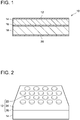
- the heat radiation device 10 includes a laminate structure in which a plurality of layers is laminated, and includes a heat generating layer 16 (which is an example of a heat source), a first support substrate 14 arranged on a front surface side of the heat generating layer 16, a MIM structure layer 12 arranged on a front surface side of the first support substrate 14, a second support substrate 18 arranged on a rear surface side of the heat generating layer 16, and a rear-surface metal layer 20 arranged on a rear surface side of the second support substrate 18.
- the heat generating layer 16 is a layer that converts inputted electric energy to heat energy.
- various types of known heat generating layers may be used, and for example, a layer formed by pattern-printing a heat generating wire (conductive material) on a front surface of the second support substrate 18, or a carbon sheet heater may be used.
- the heat generating layer 16 is connected to an external power source (not shown), and the electric energy is supplied from the external power source.
- a heat energy quantity generated in the heat generating layer 16 is controlled by an electric energy quantity supplied from the external power source being controlled.
- the heat generating layer 16 is arranged between the first support substrate 14 and the second support substrate 18, so the heat energy generated in the heat generating layer 16 flows to a first support substrate 14 side and a second support substrate 18 side.
- the first support substrate 14 is in contact with a front surface of the heat generating layer 16.
- the first support substrate 14 may be constituted of a material with a large heat conductivity, and for example, an aluminum nitride (AlN) substrate or a silicon carbide (SiC) substrate may be used.
- AlN aluminum nitride
- SiC silicon carbide
- the first support substrate 14 and the heat generating layer 16 may be adhered by using adhesive, or may be bonded by applying pressure therebetween by using a casing or the like (by so-called pressure welding).
- the MIM (Metal-Insulator-Metal) structure layer 12 is one type of a meta-material structure layer, and is provided on a front surface of the first support substrate 14.
- the MIM structure layer 12 radiates the heat energy inputted from the heat generating layer 16 as radiant energy from a front surface thereof. That is, the MIM structure layer 12 is configured to radiate the radiant energy of a peak wavelength and in a narrow wavelength range (specific wavelength range) surrounding the peak wavelength, but configured not to radiate the radiant energy in ranges other than the specific wavelength range. That is, the MIM structure layer 12 has a high emissivity (such as 0.85 to 0.9) at the peak wavelength and an extremely low emissivity (such as 0.1 or lower) in the wavelength ranges other than the specific wavelength range.
- an average emissivity of the MIM structure layer 12 in the entire infrared wavelength range is 0.15 to 0.3.
- the specific wavelength range for example, it may have its peak wavelength (such as 5 to 7 ⁇ m) in a near-infrared wavelength range (such as 2 to 10 ⁇ m), and may have its half power width adjusted to be about 1 ⁇ m.
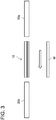
- the MIM structure layer 12 includes a first metal layer 26 provided on the front surface of the first support substrate 14, an insulation layer 24 provided on a front surface of the first metal layer 26, and a plurality of protruding metal portions 22 provided on a front surface of the insulation layer 24.
- the first metal layer 26 may be constituted of metal such as gold (Au), aluminum (Al), and molybdenum (Mo), and in this embodiment, it is constituted of gold (Au).
- the first metal layer 26 is provided over an entirety of the front surface of the first support substrate 14.
- the insulation layer 24 may be constituted of an insulation material such as ceramic, and in this embodiment, it is constituted of aluminum oxide (Al 2 O 3 ).
- the insulation layer 24 is provided over an entirety of the front surface of the first metal layer 26.
- the protruding metal portions 22 is given a round columnar shape by metal such as gold (Au), aluminum (Al), and molybdenum (Mo), and in this embodiment, they are constituted of gold (Au).
- the protruding metal portions 22 are provided at parts of the front surface of the insulation layer 24.
- the protruding metal portions 22 are arranged in plurality with intervals between each other in an x direction and a y direction on the front surface of the insulation layer 24.
- the peak wavelength of the radiant energy radiated from the MIM structure layer 12 can be adjusted by adjusting a dimension of the protruding metal portions 22 (diameter and height of the round columnar shape).
- the MIM structure layer 12 as aforementioned may be fabricated using a well-known nano-processing technique.
- the MIM structure layer 12 is used, however, a meta-material structure layer other than the MIM structure layer may be used.
- a microcavity structure described in JP 2015-198063 A may be provided on the front surface of the first support substrate 14.
- the second support substrate 18 is in contact with a rear surface of the heat generating layer 16.
- the second support substrate 18 may be constituted of a material having a small heat conductivity as compared to the heat conductivity of the first support substrate 14, and for example, an aluminum oxide (Al 2 O 3 ) substrate may be used.
- the second support substrate 18 and the heat generating layer 16 may be adhered by using adhesive, or may be bonded by applying pressure therebetween by using a casing or the like (by so-called pressure welding).
- a thickness of the second support substrate 18 is made larger than a thickness of the first support substrate 14.
- Thermal resistance of the second support substrate 18 is made larger than thermal resistance of the first support substrate 14 by adjusting the heat conductivities and the thicknesses. Due to this, the heat energy generated in the heat generating layer 16 flows at a larger quantity to the first support substrate 14 side than to the second support substrate 18 side.
- the rear-surface metal layer 20 is arranged on a rear surface of the second support substrate 18.
- the rear-surface metal layer 20 is constituted of a metal material with a low emissivity (such as gold (Au) and aluminum (Al)).
- the rear-surface metal layer 20 is constituted of gold (Au). Due to this, an average emissivity of the rear-surface metal layer 20 in the entire infrared wavelength range is about 0.05. Thus, the average emissivity of the rear-surface metal layer 20 is set smaller than the average emissivity of the MIM structure layer 12.
- the rear-surface metal layer 20 may be fabricated by using sputtering on an entirety of the rear surface of the second support substrate 18.
- the electric energy is supplied to the heat generating layer 16. Due to this, the heat generating layer 16 converts the electric energy to the heat energy, and the heat energy is transferred from the heat generating layer 16 to the first support substrate 14 or to the second support substrate 18.
- the first support substrate 14 has the higher heat conductivity and the smaller thickness as compared to the second support substrate 18. Due to this, the heat energy transferred from the heat generating layer 16 to the first support substrate 14 becomes larger than the heat energy transferred from the heat generating layer 16 to the second support substrate 18. Due to this, a temperature of the first support substrate 14 becomes higher than a temperature of the second support substrate 18.
- the heat energy transferred to the first support substrate 14 is transferred (inputted) to the MIM structure layer 12.
- the MIM structure layer 12 radiates the heat energy inputted from the first support substrate 14 as the radiant energy from the front surface thereof.
- the heat energy transferred to the second support substrate 18 is transferred to the rear-surface metal layer 20, and is radiated from the rear surface of the rear-surface metal layer 20.
- the temperature of the second support substrate 18 is lower than the temperature of the first support substrate 14, by which a temperature of the rear-surface metal layer 20 also becomes low. Due to this as well, the quantity of the radiant energy radiated from the rear-surface metal layer 20 can be suppressed.
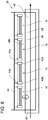
- FIG. 3 a heat balance calculation for a case of heating a workpiece W (which is an example of a target object) using the aforementioned heat radiation device 10 will be described with reference to FIG. 3 .
- the heat radiation device 10 is arranged with the MIM structure layer 12 facing downward, and the MIM structure layer 12 faces the workpiece W.
- Furnace walls 30a, 30b constituted of SUS are arranged on right and left sides of the heat radiation device 10. Further, air in a furnace flows in a direction of an arrow in upper and lower spaces in the heat radiation device 10.
- the heat balance calculation was performed under a condition in which the electric energy is supplied to the heat generating layer 16 so that the front surface temperature of the MIM structure layer 12 is set to 280°C.
- the heat radiation device of the comparative example includes the first support substrate 14 and the MIM structure layer 12 similar to the heat radiation device 10, however, it differs in that it uses a ceramic heater 32 instead of the heat generating layer 16, and the second support substrate 18 and the rear-surface metal layer 20 are not arranged on a rear side of the ceramic heater 32 (which is an upper side in FIG. 4 ).
- the heat radiation device of the comparative example is arranged to face the workpiece W, and furnace walls 34d, 34e constituted of SUS are arranged on left and right sides thereof.
- insulation members 34a, 34b, 34c are arranged on a rear surface side of the heat radiation device of the comparative example (which is the upper side in FIG. 4 ), by which heat insulation of the ceramic heater 32 is implemented. Further, to prevent heat transfer from the ceramic heater 32, a space is provided between the ceramic heater 32 and the insulation member 34a.
- a condition of the heat balance calculation was set identical to that of FIG. 3 . That is, the calculation was performed under the condition in which electric energy is supplied to the ceramic heater 32 so that the front surface temperature of the MIM structure layer 12 is set to 280°C.
- the heat radiation device 10 of the present embodiment suppresses the heat loss from the rear-surface metal layer 20 at a lower degree, and the workpiece W can be heated efficiently with less electric energy.
- the heat radiation device of the comparative example FIG. 4
- the heat loss is still large despite the arrangement of the insulation members 34a to 34c as based on a conventional general concept, and the electric energy is required at a greater quantity.
- the processing device shown in FIG. 5 includes a furnace body 40 (which is an example of a housing) and a plurality of heat radiation devices 10 housed in a space 46 in the furnace body 40.
- the plurality of heat radiation devices 10 is arranged with an interval between each other in a transport direction of the workpiece W.
- Each of the heat radiation devices 10 is arranged so that the MIM structure layer thereof faces downward.
- the rear-surface metal layer 20 of each heat radiation device 10 faces an inner wall surface 40a of the furnace body 40.
- the inner wall surface 40a may be constituted of materials with a high reflectivity, such as SUS.
- Each of the plurality of heat radiation devices 10 is held on the inner wall surface 40a of the furnace body 40 using holder members 44a, 44b (which are examples of a holder).
- Casings 42a, 42b are attached to both left and right ends of each heat radiation device 10.
- the casings 42a, 42b are in contact with the heat radiation device 10 only at the ends of the heat radiation device 10.
- An upper end of the holder member 44a is fixed to the inner wall surface 40a, and a lower end of the holder member 44a is fixed to the casing 42a.
- an upper end of the holder member 44b is fixed to the inner wall surface 40a, and a lower end of the holder member 44b is fixed to the casing 42b.
- the heat radiation device 10 is thereby held on the inner wall surface 40a of the furnace body 40.
- the rear-surface metal layers 20 of the heat radiation devices 10 do not directly contact the inner wall surface 40a, and spaces 49 are provided therebetween.
- the workpiece W is transported in the furnace body 40 along an arrow 48.
- the workpiece W transported in the furnace body 40 is radiated with the radiant energy in the specific wavelength range from each of the plurality of heat radiation device 10. Further, the workpiece W is heated by heat transfer caused by the convection of the air flowing in the furnace.
- the heat radiation devices 10 are connected to the furnace body 40 only at their ends via the casings 42a, 42b and the holder members 44a, 44b. Due to this, the heat loss caused by heat transfer from the heat radiation devices 10 to the furnace body 40 can effectively be suppressed.
- the rear-surface metal layers 20 of the heat radiation devices 10 and the inner wall surface 40a of the furnace body 40 face each other with the spaces 49 in between them, so the heat loss by radiation from the rear-surface metal layers 20 is generated.
- the emissivity of the rear-surface metal layers 20 is set low, the heat loss by the radiation from the rear-surface metal layers 20 to the inner wall surface 40a can be suppressed low. Due to this, the processing device shown in FIG. 5 can efficiently radiate the radiant energy in the specific wavelength range onto the workpiece W.
- the heat radiation device 10 of the present embodiment can be used in a processing device shown in FIG. 6 .
- the processing device shown in FIG. 6 unlike the processing device shown in FIG. 5 , it differs greatly in that a space in a furnace body 50 is partitioned by a muffle plate 58 (which is an example of a partition plate), and a space 56b housing the heat radiation device 10 and a space 56a in which the workpiece W is transported.
- the furnace body 50 includes a main body 54 including the space 56a where the workpiece W is transported and a support beam 52 provided above the main body 54. An opening at an upper end of the main body 54 is closed by the muffle plate 58.
- the muffle plate 58 is constituted of a material through which the radiant energy in the specific wavelength range radiated from the heat radiation devices 10 passes.
- the support beam 52 holds a plurality of heat radiation devices 10.
- a holding structure that holds the heat radiation devices 10 on the support beam 52 is identical to a holding structure in the processing device shown in FIG. 5 .
- the radiant energy in the specific wavelength range radiated from the respective heat radiation devices 10 passes through the muffle plate 58 and is radiated onto the workpiece W. Due to this, heating of the workpiece W is implemented. Further, since the muffle plate 58 is provided between the heat radiation devices 10 and the workpiece W, heat energy other than the radiant energy radiated from the heat radiation devices 10 can further be suppressed from being transferred to the workpiece W. As a result, as compared to the processing device shown in FIG. 5 , an increase in the temperature of the workpiece W can further be suppressed.
- the heat radiation devices 10 of the present embodiments can effectively suppress the heat loss from the rear-surface metal layers 20, so a greater quantity of the radiant energy in the specific wavelength range can be outputted with less electric energy. Due to this, the heating process of the workpiece W (such as the drying process of the solvent) can be performed with less energy in a short period of time.
Landscapes
- Engineering & Computer Science (AREA)
- Chemical & Material Sciences (AREA)
- Mechanical Engineering (AREA)
- General Engineering & Computer Science (AREA)
- Ceramic Engineering (AREA)
- Combustion & Propulsion (AREA)
- Inorganic Chemistry (AREA)
- Life Sciences & Earth Sciences (AREA)
- Microbiology (AREA)
- Drying Of Solid Materials (AREA)
- Resistance Heating (AREA)
- Health & Medical Sciences (AREA)
- Toxicology (AREA)
- Container, Conveyance, Adherence, Positioning, Of Wafer (AREA)
- Physical Or Chemical Processes And Apparatus (AREA)
Abstract
Description
- The technique disclosed herein relates to a heat radiation device configured to radiate radiant energy of a specific wavelength by using a meta-material structure layer.
-
JP 2015-198063 A - As aforementioned, in a heat radiation device using a meta-material structure, heat energy outputted from a heat source can be radiated as radiant energy of a specific wavelength from a surface on a meta-material structure layer side. However, in a conventional heat radiation device, a quantity of heat energy emitted from surfaces other than the surface on the meta-material structure layer side is large, and there had been a problem that a large heat energy loss thereby occurs. The description herein provides a heat radiation device capable of suppressing a heat energy loss as compared to the conventional heat radiation device.
- A heat radiation device disclosed in the disclosure comprises: a heat source; a meta-material structure layer arranged on a front surface side of the heat source and configured to radiate radiant energy in a specific wavelength range by converting heat energy inputted from the heat source into the radiant energy in the specific wavelength range; and a rear-surface metal layer arranged on a rear surface side of the heat source, wherein an average emissivity of the rear-surface metal layer is smaller than an average emissivity of the meta-material structure layer.
- In the above heat radiation device, the heat source is arranged between the meta-material structure layer and the rear-surface metal layer. Further, the emissivity of the rear-surface metal layer is smaller than the emissivity of the meta-material structure layer. Due to this, a heat energy loss from the rear-surface metal layer is suppressed small, and the heat energy loss can be suppressed as compared to a conventional heat radiation device.
- Here, the "average emissivity" as above means an average emissivity over an entire infrared wavelength range (0.7µm to 1mm). Thus, "an average emissivity of the rear-surface metal layer is smaller than an average emissivity of the meta-material structure layer" as above stands true even if the emissivity of the rear-surface metal layer is larger in a part of the wavelength range, so long as the average emissivity of the rear-surface metal layer is smaller than the average emissivity of the meta-material structure layer in the entire infrared wavelength range.
- Further, the "average emissivity" as above means an "average emissivity" measured upon when the rear-surface metal layer and the meta-material structure layer are set to a same setting temperature. Due to this, in a case where a temperature of the rear-surface metal layer and a temperature of the meta-material structure layer differ upon operating the heat radiation device, the "average emissivity" is measured by bringing the rear-surface metal layer to the setting temperature and the "average emissivity" is measured by bringing the meta-material structure layer to the setting temperature, and a magnitude comparison is performed based on these measured "average emissivity". The "setting temperature" as above may for example be a temperature of the meta-material structure layer or a temperature of the rear-surface metal layer when the heat radiation device is operated at a rated output.
- Further, the description herein discloses a novel processing device configured to process a target object using the heat radiation device as above. The processing device disclosed herein comprises the heat radiation device as described above arranged to face the target object; a housing that houses the target object and the heat radiation device; and a holder that holds the heat radiation device in the housing, with one end of the holder attached to an inner wall surface of the housing and another end of the holder attached to a part of the heat radiation device. The meta-material structure layer of the heat radiation device faces the target object. The rear-surface metal layer of the heat radiation device faces the inner wall surface of the housing. A gap is provided between the rear-surface metal layer and the inner wall surface of the housing.
- According to the processing device as above, the heat energy loss caused by the radiation from the rear-surface metal layer can be suppressed, and in addition a heat energy loss caused by thermal conduction from the rear-surface metal layer can be suppressed. Due to this, the processing of the target object using the heat radiation device can be performed effectively.
-
-
FIG. 1 is a vertical cross-sectional view of a heat radiation device of a present embodiment. -
FIG. 2 is an enlarged view of a primary portion that schematically shows a structure of a MIM structure layer. -
FIG. 3 is a diagram for explaining an example of a heat balance of the heat radiation device according to the embodiment. -
FIG. 4 is a diagram for explaining an example of a heat balance of a heat radiation device according to a comparative example. -
FIG 5 is a cross-sectional view schematically showing a structure of a processing device using the heat radiation device of the present embodiment. -
FIG. 6 is a cross-sectional view schematically showing a structure of another processing device using the heat radiation device of the present embodiment. - Firstly, some features of embodiments described hereinbelow will be listed. Each of the features listed herein exhibits usefulness by being employed individually.
- (Feature 1) In a heat radiation device disclosed herein, a meta-material structure layer may be arranged on a front surface of a first support substrate. A rear-surface metal layer may be arranged on a rear surface of a second support substrate. A heat source may be arranged between the first support substrate and the second support substrate. Further, a heat conductivity of the second support substrate may be smaller than a heat conductivity of the first support substrate. According to such a configuration, the heat energy flowing from the heat source to the second support substrate can be suppressed low, and a heat energy loss from the rear-surface metal layer can suitably be suppressed.
- (Feature 2) In the heat radiation device disclosed herein, the first support substrate may be an AlN substrate. The second support substrate may be an Al2O3 substrate. The rear-surface metal layer may be an Au layer. According to such a configuration, a heat loss from the Au layer being the rear-surface metal layer can suitably be suppressed.
- (Feature 3) In the heat radiation device disclosed herein, a thickness of the first support substrate may be smaller than a thickness of the second support substrate. According to such a configuration, heat from the heat source flows easily to the first support substrate being a substrate on a meta-material structure layer side, by which the heat energy from the heat source can more effectively be utilized.
- (Feature 4) In a processing device using the heat radiation device disclosed herein, a partition wall partitioning a space in a housing into a first space in which a target object is housed and a second space in which the heat radiation device is housed may further be comprised. The partition wall may allow radiant energy in a specific wavelength range to pass therethrough. According to such a configuration, a temperature rise in the target object can suitably be suppressed. On the other hand, a process to radiate the radiant energy of a specific wavelength range on the target object can be performed.
- (Feature 5) In the processing device using the heat radiation device disclosed herein, a drying process may be executed on the target object in the housing.
- The
heat radiation device 10 of the present embodiment is a heat radiation device (emitter) configured to radiate radiant energy in a specific wavelength range in an entire infrared wavelength range (0.7µm to 1mm). As shown inFIG 1 , theheat radiation device 10 includes a laminate structure in which a plurality of layers is laminated, and includes a heat generating layer 16 (which is an example of a heat source), afirst support substrate 14 arranged on a front surface side of theheat generating layer 16, aMIM structure layer 12 arranged on a front surface side of thefirst support substrate 14, asecond support substrate 18 arranged on a rear surface side of theheat generating layer 16, and a rear-surface metal layer 20 arranged on a rear surface side of thesecond support substrate 18. - The heat generating
layer 16 is a layer that converts inputted electric energy to heat energy. As the heat generatinglayer 16, various types of known heat generating layers may be used, and for example, a layer formed by pattern-printing a heat generating wire (conductive material) on a front surface of thesecond support substrate 18, or a carbon sheet heater may be used. Theheat generating layer 16 is connected to an external power source (not shown), and the electric energy is supplied from the external power source. A heat energy quantity generated in theheat generating layer 16 is controlled by an electric energy quantity supplied from the external power source being controlled. Theheat generating layer 16 is arranged between thefirst support substrate 14 and thesecond support substrate 18, so the heat energy generated in theheat generating layer 16 flows to afirst support substrate 14 side and asecond support substrate 18 side. - The
first support substrate 14 is in contact with a front surface of theheat generating layer 16. Thefirst support substrate 14 may be constituted of a material with a large heat conductivity, and for example, an aluminum nitride (AlN) substrate or a silicon carbide (SiC) substrate may be used. Thefirst support substrate 14 and theheat generating layer 16 may be adhered by using adhesive, or may be bonded by applying pressure therebetween by using a casing or the like (by so-called pressure welding). - The MIM (Metal-Insulator-Metal)
structure layer 12 is one type of a meta-material structure layer, and is provided on a front surface of thefirst support substrate 14. TheMIM structure layer 12 radiates the heat energy inputted from theheat generating layer 16 as radiant energy from a front surface thereof. That is, theMIM structure layer 12 is configured to radiate the radiant energy of a peak wavelength and in a narrow wavelength range (specific wavelength range) surrounding the peak wavelength, but configured not to radiate the radiant energy in ranges other than the specific wavelength range. That is, theMIM structure layer 12 has a high emissivity (such as 0.85 to 0.9) at the peak wavelength and an extremely low emissivity (such as 0.1 or lower) in the wavelength ranges other than the specific wavelength range. Due to this, an average emissivity of theMIM structure layer 12 in the entire infrared wavelength range (0.7µm to 1mm) is 0.15 to 0.3. As the specific wavelength range, for example, it may have its peak wavelength (such as 5 to 7µm) in a near-infrared wavelength range (such as 2 to 10µm), and may have its half power width adjusted to be about 1µm. - As shown in
FIG. 2 , theMIM structure layer 12 includes afirst metal layer 26 provided on the front surface of thefirst support substrate 14, an insulation layer 24 provided on a front surface of thefirst metal layer 26, and a plurality of protrudingmetal portions 22 provided on a front surface of the insulation layer 24. Thefirst metal layer 26 may be constituted of metal such as gold (Au), aluminum (Al), and molybdenum (Mo), and in this embodiment, it is constituted of gold (Au). Thefirst metal layer 26 is provided over an entirety of the front surface of thefirst support substrate 14. The insulation layer 24 may be constituted of an insulation material such as ceramic, and in this embodiment, it is constituted of aluminum oxide (Al2O3). The insulation layer 24 is provided over an entirety of the front surface of thefirst metal layer 26. The protrudingmetal portions 22 is given a round columnar shape by metal such as gold (Au), aluminum (Al), and molybdenum (Mo), and in this embodiment, they are constituted of gold (Au). The protrudingmetal portions 22 are provided at parts of the front surface of the insulation layer 24. The protrudingmetal portions 22 are arranged in plurality with intervals between each other in an x direction and a y direction on the front surface of the insulation layer 24. The peak wavelength of the radiant energy radiated from theMIM structure layer 12 can be adjusted by adjusting a dimension of the protruding metal portions 22 (diameter and height of the round columnar shape). Further, by adjusting an arrangement pattern of the protruding metal portions 22 (the intervals between the adjacent protruding metal portions 22), a range limits of the aforementioned "specific wavelength range" can be adjusted. TheMIM structure layer 12 as aforementioned may be fabricated using a well-known nano-processing technique. - In the
heat radiation device 10 of the present embodiment, theMIM structure layer 12 is used, however, a meta-material structure layer other than the MIM structure layer may be used. For example, a microcavity structure described inJP 2015-198063 A first support substrate 14. - The
second support substrate 18 is in contact with a rear surface of theheat generating layer 16. Thesecond support substrate 18 may be constituted of a material having a small heat conductivity as compared to the heat conductivity of thefirst support substrate 14, and for example, an aluminum oxide (Al2O3) substrate may be used. Thesecond support substrate 18 and theheat generating layer 16 may be adhered by using adhesive, or may be bonded by applying pressure therebetween by using a casing or the like (by so-called pressure welding). As it is apparent fromFIG. 1 , a thickness of thesecond support substrate 18 is made larger than a thickness of thefirst support substrate 14. Thermal resistance of thesecond support substrate 18 is made larger than thermal resistance of thefirst support substrate 14 by adjusting the heat conductivities and the thicknesses. Due to this, the heat energy generated in theheat generating layer 16 flows at a larger quantity to thefirst support substrate 14 side than to thesecond support substrate 18 side. - The rear-
surface metal layer 20 is arranged on a rear surface of thesecond support substrate 18. The rear-surface metal layer 20 is constituted of a metal material with a low emissivity (such as gold (Au) and aluminum (Al)). In this embodiment, the rear-surface metal layer 20 is constituted of gold (Au). Due to this, an average emissivity of the rear-surface metal layer 20 in the entire infrared wavelength range is about 0.05. Thus, the average emissivity of the rear-surface metal layer 20 is set smaller than the average emissivity of theMIM structure layer 12. The rear-surface metal layer 20 may be fabricated by using sputtering on an entirety of the rear surface of thesecond support substrate 18. - In order to radiate the radiant energy (infrared beam) in the specific wavelength range from the aforementioned
heat radiation device 10, the electric energy is supplied to theheat generating layer 16. Due to this, theheat generating layer 16 converts the electric energy to the heat energy, and the heat energy is transferred from theheat generating layer 16 to thefirst support substrate 14 or to thesecond support substrate 18. Here, thefirst support substrate 14 has the higher heat conductivity and the smaller thickness as compared to thesecond support substrate 18. Due to this, the heat energy transferred from theheat generating layer 16 to thefirst support substrate 14 becomes larger than the heat energy transferred from theheat generating layer 16 to thesecond support substrate 18. Due to this, a temperature of thefirst support substrate 14 becomes higher than a temperature of thesecond support substrate 18. - The heat energy transferred to the
first support substrate 14 is transferred (inputted) to theMIM structure layer 12. TheMIM structure layer 12 radiates the heat energy inputted from thefirst support substrate 14 as the radiant energy from the front surface thereof. On the other hand, the heat energy transferred to thesecond support substrate 18 is transferred to the rear-surface metal layer 20, and is radiated from the rear surface of the rear-surface metal layer 20. Here, since the emissivity of the rear-surface metal layer 20 is set low, the quantity of the radiant energy radiated from the rear-surface metal layer 20 is thereby suppressed. Further, as aforementioned, the temperature of thesecond support substrate 18 is lower than the temperature of thefirst support substrate 14, by which a temperature of the rear-surface metal layer 20 also becomes low. Due to this as well, the quantity of the radiant energy radiated from the rear-surface metal layer 20 can be suppressed. - Here, a heat balance calculation for a case of heating a workpiece W (which is an example of a target object) using the aforementioned
heat radiation device 10 will be described with reference toFIG. 3 . As shown inFIG. 3 , theheat radiation device 10 is arranged with theMIM structure layer 12 facing downward, and theMIM structure layer 12 faces the workpieceW. Furnace walls heat radiation device 10. Further, air in a furnace flows in a direction of an arrow in upper and lower spaces in theheat radiation device 10. The heat balance calculation was performed under a condition in which the electric energy is supplied to theheat generating layer 16 so that the front surface temperature of theMIM structure layer 12 is set to 280°C. As a result of the calculation, about 20% of the heat energy inputted to theheat generating layer 16 was radiated onto the workpiece W as the radiant energy from theheat radiation device 10, about 20% was used for heating the workpiece W by convective heat transfer from theheat radiation device 10, and about 60% of the remaining became a heat energy loss. The heat energy loss was broken down primarily to a heat loss by heat transfer from theheat radiation device 10 to thefurnace walls surface metal layer 20 of theheat radiation device 10. That is, the heat loss by radiation from the rear-surface metal layer 20 hardly occurred. - Next, a heat balance calculation for a case of heating the workpiece W using a heat radiation device of a comparative example will be described with reference to
FIG 4 . The heat radiation device of the comparative example includes thefirst support substrate 14 and theMIM structure layer 12 similar to theheat radiation device 10, however, it differs in that it uses aceramic heater 32 instead of theheat generating layer 16, and thesecond support substrate 18 and the rear-surface metal layer 20 are not arranged on a rear side of the ceramic heater 32 (which is an upper side inFIG. 4 ). As it is apparent fromFIG. 4 , the heat radiation device of the comparative example is arranged to face the workpiece W, andfurnace walls insulation members FIG. 4 ), by which heat insulation of theceramic heater 32 is implemented. Further, to prevent heat transfer from theceramic heater 32, a space is provided between theceramic heater 32 and theinsulation member 34a. A condition of the heat balance calculation was set identical to that ofFIG. 3 . That is, the calculation was performed under the condition in which electric energy is supplied to theceramic heater 32 so that the front surface temperature of theMIM structure layer 12 is set to 280°C. As a result of the calculation, about 10% of the heat energy inputted to theceramic heater 32 was radiated onto the workpiece W as radiant energy, about 10% was used for heating the workpiece W by convective heat transfer, and about 80% of the remaining became a heat energy loss. The heat energy loss was broken down primarily to a heat loss by heat transfer to thefurnace walls insulation members - As it is apparent from the heat balance calculations in
FIGS. 3 and4 as aforementioned, theheat radiation device 10 of the present embodiment (FIG. 3 ) suppresses the heat loss from the rear-surface metal layer 20 at a lower degree, and the workpiece W can be heated efficiently with less electric energy. On the other hand, in the heat radiation device of the comparative example (FIG. 4 ), it has been found that the heat loss is still large despite the arrangement of theinsulation members 34a to 34c as based on a conventional general concept, and the electric energy is required at a greater quantity. - Next, an example of a processing device configured to process a workpiece using the
heat radiation device 10 of the present embodiment will be described with reference toFIG. 5 . The processing device shown inFIG. 5 includes a furnace body 40 (which is an example of a housing) and a plurality ofheat radiation devices 10 housed in aspace 46 in thefurnace body 40. The plurality ofheat radiation devices 10 is arranged with an interval between each other in a transport direction of the workpiece W. Each of theheat radiation devices 10 is arranged so that the MIM structure layer thereof faces downward. Thus, the rear-surface metal layer 20 of eachheat radiation device 10 faces aninner wall surface 40a of thefurnace body 40. Theinner wall surface 40a may be constituted of materials with a high reflectivity, such as SUS. - Each of the plurality of
heat radiation devices 10 is held on theinner wall surface 40a of thefurnace body 40 usingholder members Casings heat radiation device 10. Thecasings heat radiation device 10 only at the ends of theheat radiation device 10. An upper end of theholder member 44a is fixed to theinner wall surface 40a, and a lower end of theholder member 44a is fixed to thecasing 42a. Similarly, an upper end of theholder member 44b is fixed to theinner wall surface 40a, and a lower end of theholder member 44b is fixed to thecasing 42b. Due to this, theheat radiation device 10 is thereby held on theinner wall surface 40a of thefurnace body 40. As it is apparent fromFIG 5 , the rear-surface metal layers 20 of theheat radiation devices 10 do not directly contact theinner wall surface 40a, andspaces 49 are provided therebetween. - To heat the workpiece W in the above processing device, the workpiece W is transported in the
furnace body 40 along anarrow 48. The workpiece W transported in thefurnace body 40 is radiated with the radiant energy in the specific wavelength range from each of the plurality ofheat radiation device 10. Further, the workpiece W is heated by heat transfer caused by the convection of the air flowing in the furnace. Here, theheat radiation devices 10 are connected to thefurnace body 40 only at their ends via thecasings holder members heat radiation devices 10 to thefurnace body 40 can effectively be suppressed. Further, the rear-surface metal layers 20 of theheat radiation devices 10 and theinner wall surface 40a of thefurnace body 40 face each other with thespaces 49 in between them, so the heat loss by radiation from the rear-surface metal layers 20 is generated. However, since the emissivity of the rear-surface metal layers 20 is set low, the heat loss by the radiation from the rear-surface metal layers 20 to theinner wall surface 40a can be suppressed low. Due to this, the processing device shown inFIG. 5 can efficiently radiate the radiant energy in the specific wavelength range onto the workpiece W. - When only the radiant energy in the specific wavelength range is radiated onto the workpiece W, only substances which absorb the radiant energy in the specific wavelength range can be heated while suppressing a temperature of the workpiece W low. For example, when a workpiece W containing a flammable solvent (such as N-methyl-pyrrolidone, methyl isobutyl ketone, butyl acetate, and toluene) (such as a substrate including a coated layer (the solvent being contained in the coated layer)) is to be subjected to a drying process, only the solvent can be evaporated while suppressing the temperature of the workpiece W low by radiating only the radiant energy in the wavelength range which the solvent absorbs onto the workpiece W, and the workpiece W can thereby be dried. Since the solvent can be dried efficiently, the drying process can be performed with less power consumption and in a short period of time.
- Further, the
heat radiation device 10 of the present embodiment can be used in a processing device shown inFIG. 6 . In the processing device shown inFIG. 6 , unlike the processing device shown inFIG. 5 , it differs greatly in that a space in afurnace body 50 is partitioned by a muffle plate 58 (which is an example of a partition plate), and aspace 56b housing theheat radiation device 10 and a space 56a in which the workpiece W is transported. Specifically, as shown inFIG. 6 , thefurnace body 50 includes amain body 54 including the space 56a where the workpiece W is transported and asupport beam 52 provided above themain body 54. An opening at an upper end of themain body 54 is closed by themuffle plate 58. Themuffle plate 58 is constituted of a material through which the radiant energy in the specific wavelength range radiated from theheat radiation devices 10 passes. Thesupport beam 52 holds a plurality ofheat radiation devices 10. A holding structure that holds theheat radiation devices 10 on thesupport beam 52 is identical to a holding structure in the processing device shown inFIG. 5 . - In the processing device shown in
FIG. 6 as well, the radiant energy in the specific wavelength range radiated from the respectiveheat radiation devices 10 passes through themuffle plate 58 and is radiated onto the workpiece W. Due to this, heating of the workpiece W is implemented. Further, since themuffle plate 58 is provided between theheat radiation devices 10 and the workpiece W, heat energy other than the radiant energy radiated from theheat radiation devices 10 can further be suppressed from being transferred to the workpiece W. As a result, as compared to the processing device shown inFIG. 5 , an increase in the temperature of the workpiece W can further be suppressed. - As it is apparent from the foregoing descriptions, the
heat radiation devices 10 of the present embodiments can effectively suppress the heat loss from the rear-surface metal layers 20, so a greater quantity of the radiant energy in the specific wavelength range can be outputted with less electric energy. Due to this, the heating process of the workpiece W (such as the drying process of the solvent) can be performed with less energy in a short period of time. - Specific examples of the present invention are described above in detail, but these examples are merely illustrative and place no limitation on the scope of the patent claims. The technology described in the patent claims also encompasses various changes and modifications to the specific examples described above. Further, the technical elements explained in the present description or drawings exert technical utility independently or in combination of some of them, and the combination is not limited to one described in the claims as filed. Moreover, the technology exemplified in the present description or drawings achieves a plurality of objects at the same time, and has technical utility by achieving one of such objects.
Claims (7)
- A heat radiation device configured to radiate radiant energy in a specific wavelength range, the heat radiation device comprising:a heat source;a meta-material structure layer arranged on a front surface side of the heat source and configured to radiate the radiant energy in the specific wavelength range by converting heat energy inputted from the heat source into the radiant energy in the specific wavelength range; anda rear-surface metal layer arranged on a rear surface side of the heat source,wherein an average emissivity of the rear-surface metal layer is smaller than an average emissivity of the meta-material structure layer.
- The heat radiation device as in claim 1, wherein
the meta-material structure layer is arranged on a front surface of a first support substrate,
the rear-surface metal layer is arranged on a rear surface of a second support substrate,
the heat source is arranged between the first support substrate and the second support substrate, and
a heat conductivity of the second support substrate is smaller than a heat conductivity of the first support substrate. - The heat radiation device as in claim 2, wherein
the first support substrate is an AIN substrate,
the second support substrate is an Al2O3 substrate, and
the rear-surface metal layer is an Au layer. - The heat radiation device as in claim 2 or 3, wherein
a thickness of the first support substrate is smaller than a thickness of the second support substrate. - A processing device configured to process a target object, the processing device comprising:the heat radiation device as in any one of claims 1 to 4 arranged to face the target object;a housing that houses the target object and the heat radiation device; anda holder that holds the heat radiation device in the housing, one end of the holder attached to an inner wall surface of the housing and another end of the holder attached to a part of the heat radiation device,wherein
the meta-material structure layer of the heat radiation device faces the target object,
the rear-surface metal layer of the heat radiation device faces the inner wall surface of the housing, and
a gap is provided between the rear-surface metal layer and the inner wall surface of the housing. - The processing device as in claim 5, further comprising:a partition wall partitioning a space in the housing into a first space in which the target object is housed and a second space in which the heat radiation device is housed,wherein the partition wall allows the radiant energy in the specific wavelength range to pass therethrough.
- The processing device as in claim 5 or 6, wherein
a drying process is executed on the target object in the housing.
Applications Claiming Priority (2)
| Application Number | Priority Date | Filing Date | Title |
|---|---|---|---|
| JP2016060652 | 2016-03-24 | ||
| PCT/JP2017/010019 WO2017163986A1 (en) | 2016-03-24 | 2017-03-13 | Radiation device and processing device using same radiation device |
Publications (3)
| Publication Number | Publication Date |
|---|---|
| EP3435735A1 true EP3435735A1 (en) | 2019-01-30 |
| EP3435735A4 EP3435735A4 (en) | 2019-10-16 |
| EP3435735B1 EP3435735B1 (en) | 2020-12-02 |
Family
ID=59899498
Family Applications (1)
| Application Number | Title | Priority Date | Filing Date |
|---|---|---|---|
| EP17770029.1A Active EP3435735B1 (en) | 2016-03-24 | 2017-03-13 | Radiation device and processing device using same radiation device |
Country Status (7)
| Country | Link |
|---|---|
| US (1) | US10701762B2 (en) |
| EP (1) | EP3435735B1 (en) |
| JP (1) | JP6876677B2 (en) |
| KR (1) | KR102352533B1 (en) |
| CN (1) | CN108925146B (en) |
| TW (1) | TWI749001B (en) |
| WO (1) | WO2017163986A1 (en) |
Cited By (1)
| Publication number | Priority date | Publication date | Assignee | Title |
|---|---|---|---|---|
| US10701762B2 (en) * | 2016-03-24 | 2020-06-30 | Ngk Insulators, Ltd. | Heat radiation device, and processing device using heat radiation device |
Families Citing this family (4)
| Publication number | Priority date | Publication date | Assignee | Title |
|---|---|---|---|---|
| WO2019009288A1 (en) * | 2017-07-05 | 2019-01-10 | 日本碍子株式会社 | Infrared processing device |
| CN112005616A (en) | 2018-04-23 | 2020-11-27 | 日本碍子株式会社 | Infrared ray radiation device |
| JP6997060B2 (en) | 2018-10-05 | 2022-01-17 | 日本碍子株式会社 | Infrared radiant device |
| EP3996468A4 (en) * | 2019-07-04 | 2023-07-19 | Lintec Corporation | Heat radiant heater |
Family Cites Families (19)
| Publication number | Priority date | Publication date | Assignee | Title |
|---|---|---|---|---|
| JPH03131027A (en) * | 1989-10-17 | 1991-06-04 | Oki Electric Ind Co Ltd | High speed heat treating method and device therefor |
| CN2285542Y (en) * | 1995-04-21 | 1998-07-01 | 柏胤万 | Multi-layer composite type electric heating board |
| CN2321192Y (en) * | 1997-12-12 | 1999-05-26 | 江琦 | Ceramic infrared heat radiating device |
| AU2002241461A1 (en) * | 2000-10-11 | 2002-06-03 | Falcon Systems Engineering Corporation | Thermal image identification system |
| JP4837192B2 (en) * | 2001-06-26 | 2011-12-14 | ローム株式会社 | Heater and fixing device having the heater |
| US7132625B2 (en) * | 2002-10-03 | 2006-11-07 | Ppg Industries Ohio, Inc. | Heatable article having a configured heating member |
| WO2005003618A1 (en) * | 2003-07-04 | 2005-01-13 | Matsushita Electric Industrial Co., Ltd. | Vacuum thermal insulation material and equipment using the same |
| KR100806764B1 (en) * | 2006-08-24 | 2008-02-27 | 이교만 | Connection cap for power supply of jade-added planar heating element and planar heating element |
| JP5235469B2 (en) * | 2008-03-31 | 2013-07-10 | 富士フイルム株式会社 | Drying apparatus and optical film manufacturing method |
| CN102012060B (en) * | 2009-09-08 | 2012-12-19 | 清华大学 | Wall type electric warmer |
| JP5830468B2 (en) * | 2010-10-29 | 2015-12-09 | スタンレー電気株式会社 | Power generator |
| BR112013030779B1 (en) * | 2011-06-10 | 2020-10-27 | Saint-Gobain Glass France | composite glazing, method for producing composite glazing and use of composite glazing |
| JP5694983B2 (en) * | 2012-03-27 | 2015-04-01 | 日本碍子株式会社 | Infrared heater |
| WO2013168332A1 (en) * | 2012-05-09 | 2013-11-14 | パナソニック株式会社 | Infrared radiation element |
| US20140263278A1 (en) * | 2013-03-15 | 2014-09-18 | Solarno, Inc. | Solar selective multilayer coating |
| TW201510451A (en) * | 2013-04-11 | 2015-03-16 | Ngk Insulators Ltd | Drying furnace |
| PT3085199T (en) * | 2013-12-16 | 2018-11-29 | Saint Gobain | Heatable pane with high frequency transmission |
| JP2015198063A (en) * | 2014-04-03 | 2015-11-09 | 日本碍子株式会社 | infrared heater |
| CN108925146B (en) * | 2016-03-24 | 2022-02-11 | 日本碍子株式会社 | Radiation device and treatment device using radiation device |
-
2017
- 2017-03-13 CN CN201780019839.1A patent/CN108925146B/en active Active
- 2017-03-13 JP JP2018507242A patent/JP6876677B2/en active Active
- 2017-03-13 EP EP17770029.1A patent/EP3435735B1/en active Active
- 2017-03-13 KR KR1020187030409A patent/KR102352533B1/en active Active
- 2017-03-13 WO PCT/JP2017/010019 patent/WO2017163986A1/en not_active Ceased
- 2017-03-22 TW TW106109504A patent/TWI749001B/en active
-
2018
- 2018-09-20 US US16/136,542 patent/US10701762B2/en active Active
Cited By (1)
| Publication number | Priority date | Publication date | Assignee | Title |
|---|---|---|---|---|
| US10701762B2 (en) * | 2016-03-24 | 2020-06-30 | Ngk Insulators, Ltd. | Heat radiation device, and processing device using heat radiation device |
Also Published As
| Publication number | Publication date |
|---|---|
| KR20180124110A (en) | 2018-11-20 |
| CN108925146B (en) | 2022-02-11 |
| TW201803403A (en) | 2018-01-16 |
| TWI749001B (en) | 2021-12-11 |
| WO2017163986A1 (en) | 2017-09-28 |
| KR102352533B1 (en) | 2022-01-19 |
| EP3435735B1 (en) | 2020-12-02 |
| US10701762B2 (en) | 2020-06-30 |
| JPWO2017163986A1 (en) | 2019-01-31 |
| EP3435735A4 (en) | 2019-10-16 |
| CN108925146A (en) | 2018-11-30 |
| US20190021139A1 (en) | 2019-01-17 |
| JP6876677B2 (en) | 2021-05-26 |
Similar Documents
| Publication | Publication Date | Title |
|---|---|---|
| US10701762B2 (en) | Heat radiation device, and processing device using heat radiation device | |
| CN101500452B (en) | radiant heater | |
| KR20190035889A (en) | Infrared Panel Radiator | |
| JP2010502930A (en) | Equipment and methods for thermal cycling | |
| TW201831041A (en) | Infrared heater | |
| JP6692046B2 (en) | Infrared heater | |
| CN105308735B (en) | Low emissivity electrostatic chuck and there is its ion implantation system | |
| TW201929057A (en) | Substrate processing apparatus and method of processing substrate and manufacturing processed workpiece | |
| KR20200058493A (en) | Organic film forming device | |
| JP2006286222A (en) | Plate type far infrared heater for vacuum heating furnace | |
| EP3787372B1 (en) | Infrared radiation device | |
| KR20180128536A (en) | Quartz heater | |
| KR20200108569A (en) | Film radiation heater | |
| JP6487621B2 (en) | Infrared light source | |
| KR102351851B1 (en) | Heater core, heater and heating system including thereof | |
| KR102351852B1 (en) | Heater and heating system including thereof | |
| KR20090043935A (en) | Far Infrared Explosion Proof Heater | |
| US12104864B2 (en) | Thermal metamaterials for directional emission in heat transfer systems | |
| KR100771381B1 (en) | Heating element for LCD substrate | |
| KR101694142B1 (en) | Hot plate for glass dry | |
| EP3582237A1 (en) | Ptc heating arrangement | |
| Kozlov et al. | Channel model of ceramic plate heating with help of microwave space | |
| JP2018006041A (en) | Tubular heater and heating device having the same | |
| JPH05144557A (en) | Heater | |
| JP2009162391A (en) | Far infrared heating device |
Legal Events
| Date | Code | Title | Description |
|---|---|---|---|
| STAA | Information on the status of an ep patent application or granted ep patent |
Free format text: STATUS: THE INTERNATIONAL PUBLICATION HAS BEEN MADE |
|
| PUAI | Public reference made under article 153(3) epc to a published international application that has entered the european phase |
Free format text: ORIGINAL CODE: 0009012 |
|
| STAA | Information on the status of an ep patent application or granted ep patent |
Free format text: STATUS: REQUEST FOR EXAMINATION WAS MADE |
|
| 17P | Request for examination filed |
Effective date: 20181012 |
|
| AK | Designated contracting states |
Kind code of ref document: A1 Designated state(s): AL AT BE BG CH CY CZ DE DK EE ES FI FR GB GR HR HU IE IS IT LI LT LU LV MC MK MT NL NO PL PT RO RS SE SI SK SM TR |
|
| AX | Request for extension of the european patent |
Extension state: BA ME |
|
| DAV | Request for validation of the european patent (deleted) | ||
| DAX | Request for extension of the european patent (deleted) | ||
| RIN1 | Information on inventor provided before grant (corrected) |
Inventor name: KONDO, YOSHIO |
|
| A4 | Supplementary search report drawn up and despatched |
Effective date: 20190918 |
|
| RIC1 | Information provided on ipc code assigned before grant |
Ipc: H05B 3/66 20060101ALI20190912BHEP Ipc: F26B 15/12 20060101ALI20190912BHEP Ipc: H05B 3/10 20060101AFI20190912BHEP Ipc: H05B 3/12 20060101ALI20190912BHEP Ipc: H05B 3/28 20060101ALI20190912BHEP Ipc: F26B 3/30 20060101ALI20190912BHEP Ipc: H05B 3/26 20060101ALI20190912BHEP |
|
| GRAP | Despatch of communication of intention to grant a patent |
Free format text: ORIGINAL CODE: EPIDOSNIGR1 |
|
| STAA | Information on the status of an ep patent application or granted ep patent |
Free format text: STATUS: GRANT OF PATENT IS INTENDED |
|
| INTG | Intention to grant announced |
Effective date: 20200707 |
|
| GRAS | Grant fee paid |
Free format text: ORIGINAL CODE: EPIDOSNIGR3 |
|
| GRAA | (expected) grant |
Free format text: ORIGINAL CODE: 0009210 |
|
| STAA | Information on the status of an ep patent application or granted ep patent |
Free format text: STATUS: THE PATENT HAS BEEN GRANTED |
|
| AK | Designated contracting states |
Kind code of ref document: B1 Designated state(s): AL AT BE BG CH CY CZ DE DK EE ES FI FR GB GR HR HU IE IS IT LI LT LU LV MC MK MT NL NO PL PT RO RS SE SI SK SM TR |
|
| REG | Reference to a national code |
Ref country code: GB Ref legal event code: FG4D |
|
| REG | Reference to a national code |
Ref country code: AT Ref legal event code: REF Ref document number: 1342380 Country of ref document: AT Kind code of ref document: T Effective date: 20201215 Ref country code: CH Ref legal event code: EP |
|
| REG | Reference to a national code |
Ref country code: IE Ref legal event code: FG4D |
|
| REG | Reference to a national code |
Ref country code: DE Ref legal event code: R096 Ref document number: 602017028841 Country of ref document: DE |
|
| PG25 | Lapsed in a contracting state [announced via postgrant information from national office to epo] |
Ref country code: RS Free format text: LAPSE BECAUSE OF FAILURE TO SUBMIT A TRANSLATION OF THE DESCRIPTION OR TO PAY THE FEE WITHIN THE PRESCRIBED TIME-LIMIT Effective date: 20201202 Ref country code: NO Free format text: LAPSE BECAUSE OF FAILURE TO SUBMIT A TRANSLATION OF THE DESCRIPTION OR TO PAY THE FEE WITHIN THE PRESCRIBED TIME-LIMIT Effective date: 20210302 Ref country code: FI Free format text: LAPSE BECAUSE OF FAILURE TO SUBMIT A TRANSLATION OF THE DESCRIPTION OR TO PAY THE FEE WITHIN THE PRESCRIBED TIME-LIMIT Effective date: 20201202 Ref country code: GR Free format text: LAPSE BECAUSE OF FAILURE TO SUBMIT A TRANSLATION OF THE DESCRIPTION OR TO PAY THE FEE WITHIN THE PRESCRIBED TIME-LIMIT Effective date: 20210303 |
|
| REG | Reference to a national code |
Ref country code: NL Ref legal event code: MP Effective date: 20201202 |
|
| REG | Reference to a national code |
Ref country code: AT Ref legal event code: MK05 Ref document number: 1342380 Country of ref document: AT Kind code of ref document: T Effective date: 20201202 |
|
| PG25 | Lapsed in a contracting state [announced via postgrant information from national office to epo] |
Ref country code: BG Free format text: LAPSE BECAUSE OF FAILURE TO SUBMIT A TRANSLATION OF THE DESCRIPTION OR TO PAY THE FEE WITHIN THE PRESCRIBED TIME-LIMIT Effective date: 20210302 Ref country code: PL Free format text: LAPSE BECAUSE OF FAILURE TO SUBMIT A TRANSLATION OF THE DESCRIPTION OR TO PAY THE FEE WITHIN THE PRESCRIBED TIME-LIMIT Effective date: 20201202 Ref country code: LV Free format text: LAPSE BECAUSE OF FAILURE TO SUBMIT A TRANSLATION OF THE DESCRIPTION OR TO PAY THE FEE WITHIN THE PRESCRIBED TIME-LIMIT Effective date: 20201202 Ref country code: SE Free format text: LAPSE BECAUSE OF FAILURE TO SUBMIT A TRANSLATION OF THE DESCRIPTION OR TO PAY THE FEE WITHIN THE PRESCRIBED TIME-LIMIT Effective date: 20201202 |
|
| PG25 | Lapsed in a contracting state [announced via postgrant information from national office to epo] |
Ref country code: NL Free format text: LAPSE BECAUSE OF FAILURE TO SUBMIT A TRANSLATION OF THE DESCRIPTION OR TO PAY THE FEE WITHIN THE PRESCRIBED TIME-LIMIT Effective date: 20201202 Ref country code: HR Free format text: LAPSE BECAUSE OF FAILURE TO SUBMIT A TRANSLATION OF THE DESCRIPTION OR TO PAY THE FEE WITHIN THE PRESCRIBED TIME-LIMIT Effective date: 20201202 |
|
| REG | Reference to a national code |
Ref country code: LT Ref legal event code: MG9D |
|
| PG25 | Lapsed in a contracting state [announced via postgrant information from national office to epo] |
Ref country code: SM Free format text: LAPSE BECAUSE OF FAILURE TO SUBMIT A TRANSLATION OF THE DESCRIPTION OR TO PAY THE FEE WITHIN THE PRESCRIBED TIME-LIMIT Effective date: 20201202 Ref country code: EE Free format text: LAPSE BECAUSE OF FAILURE TO SUBMIT A TRANSLATION OF THE DESCRIPTION OR TO PAY THE FEE WITHIN THE PRESCRIBED TIME-LIMIT Effective date: 20201202 Ref country code: CZ Free format text: LAPSE BECAUSE OF FAILURE TO SUBMIT A TRANSLATION OF THE DESCRIPTION OR TO PAY THE FEE WITHIN THE PRESCRIBED TIME-LIMIT Effective date: 20201202 Ref country code: LT Free format text: LAPSE BECAUSE OF FAILURE TO SUBMIT A TRANSLATION OF THE DESCRIPTION OR TO PAY THE FEE WITHIN THE PRESCRIBED TIME-LIMIT Effective date: 20201202 Ref country code: PT Free format text: LAPSE BECAUSE OF FAILURE TO SUBMIT A TRANSLATION OF THE DESCRIPTION OR TO PAY THE FEE WITHIN THE PRESCRIBED TIME-LIMIT Effective date: 20210405 Ref country code: RO Free format text: LAPSE BECAUSE OF FAILURE TO SUBMIT A TRANSLATION OF THE DESCRIPTION OR TO PAY THE FEE WITHIN THE PRESCRIBED TIME-LIMIT Effective date: 20201202 Ref country code: SK Free format text: LAPSE BECAUSE OF FAILURE TO SUBMIT A TRANSLATION OF THE DESCRIPTION OR TO PAY THE FEE WITHIN THE PRESCRIBED TIME-LIMIT Effective date: 20201202 |
|
| PG25 | Lapsed in a contracting state [announced via postgrant information from national office to epo] |
Ref country code: AT Free format text: LAPSE BECAUSE OF FAILURE TO SUBMIT A TRANSLATION OF THE DESCRIPTION OR TO PAY THE FEE WITHIN THE PRESCRIBED TIME-LIMIT Effective date: 20201202 |
|
| REG | Reference to a national code |
Ref country code: DE Ref legal event code: R097 Ref document number: 602017028841 Country of ref document: DE |
|
| PG25 | Lapsed in a contracting state [announced via postgrant information from national office to epo] |
Ref country code: IS Free format text: LAPSE BECAUSE OF FAILURE TO SUBMIT A TRANSLATION OF THE DESCRIPTION OR TO PAY THE FEE WITHIN THE PRESCRIBED TIME-LIMIT Effective date: 20210402 |
|
| PLBE | No opposition filed within time limit |
Free format text: ORIGINAL CODE: 0009261 |
|
| STAA | Information on the status of an ep patent application or granted ep patent |
Free format text: STATUS: NO OPPOSITION FILED WITHIN TIME LIMIT |
|
| PG25 | Lapsed in a contracting state [announced via postgrant information from national office to epo] |
Ref country code: IT Free format text: LAPSE BECAUSE OF FAILURE TO SUBMIT A TRANSLATION OF THE DESCRIPTION OR TO PAY THE FEE WITHIN THE PRESCRIBED TIME-LIMIT Effective date: 20201202 Ref country code: MC Free format text: LAPSE BECAUSE OF FAILURE TO SUBMIT A TRANSLATION OF THE DESCRIPTION OR TO PAY THE FEE WITHIN THE PRESCRIBED TIME-LIMIT Effective date: 20201202 Ref country code: AL Free format text: LAPSE BECAUSE OF FAILURE TO SUBMIT A TRANSLATION OF THE DESCRIPTION OR TO PAY THE FEE WITHIN THE PRESCRIBED TIME-LIMIT Effective date: 20201202 |
|
| REG | Reference to a national code |
Ref country code: CH Ref legal event code: PL |
|
| 26N | No opposition filed |
Effective date: 20210903 |
|
| PG25 | Lapsed in a contracting state [announced via postgrant information from national office to epo] |
Ref country code: SI Free format text: LAPSE BECAUSE OF FAILURE TO SUBMIT A TRANSLATION OF THE DESCRIPTION OR TO PAY THE FEE WITHIN THE PRESCRIBED TIME-LIMIT Effective date: 20201202 Ref country code: DK Free format text: LAPSE BECAUSE OF FAILURE TO SUBMIT A TRANSLATION OF THE DESCRIPTION OR TO PAY THE FEE WITHIN THE PRESCRIBED TIME-LIMIT Effective date: 20201202 |
|
| REG | Reference to a national code |
Ref country code: BE Ref legal event code: MM Effective date: 20210331 |
|
| PG25 | Lapsed in a contracting state [announced via postgrant information from national office to epo] |
Ref country code: CH Free format text: LAPSE BECAUSE OF NON-PAYMENT OF DUE FEES Effective date: 20210331 Ref country code: LU Free format text: LAPSE BECAUSE OF NON-PAYMENT OF DUE FEES Effective date: 20210313 Ref country code: LI Free format text: LAPSE BECAUSE OF NON-PAYMENT OF DUE FEES Effective date: 20210331 Ref country code: ES Free format text: LAPSE BECAUSE OF FAILURE TO SUBMIT A TRANSLATION OF THE DESCRIPTION OR TO PAY THE FEE WITHIN THE PRESCRIBED TIME-LIMIT Effective date: 20201202 Ref country code: IE Free format text: LAPSE BECAUSE OF NON-PAYMENT OF DUE FEES Effective date: 20210313 |
|
| PG25 | Lapsed in a contracting state [announced via postgrant information from national office to epo] |
Ref country code: IS Free format text: LAPSE BECAUSE OF FAILURE TO SUBMIT A TRANSLATION OF THE DESCRIPTION OR TO PAY THE FEE WITHIN THE PRESCRIBED TIME-LIMIT Effective date: 20210402 |
|
| PG25 | Lapsed in a contracting state [announced via postgrant information from national office to epo] |
Ref country code: BE Free format text: LAPSE BECAUSE OF NON-PAYMENT OF DUE FEES Effective date: 20210331 |
|
| PG25 | Lapsed in a contracting state [announced via postgrant information from national office to epo] |
Ref country code: CY Free format text: LAPSE BECAUSE OF FAILURE TO SUBMIT A TRANSLATION OF THE DESCRIPTION OR TO PAY THE FEE WITHIN THE PRESCRIBED TIME-LIMIT Effective date: 20201202 |
|
| PG25 | Lapsed in a contracting state [announced via postgrant information from national office to epo] |
Ref country code: HU Free format text: LAPSE BECAUSE OF FAILURE TO SUBMIT A TRANSLATION OF THE DESCRIPTION OR TO PAY THE FEE WITHIN THE PRESCRIBED TIME-LIMIT; INVALID AB INITIO Effective date: 20170313 |
|
| PG25 | Lapsed in a contracting state [announced via postgrant information from national office to epo] |
Ref country code: MK Free format text: LAPSE BECAUSE OF FAILURE TO SUBMIT A TRANSLATION OF THE DESCRIPTION OR TO PAY THE FEE WITHIN THE PRESCRIBED TIME-LIMIT Effective date: 20201202 |
|
| PG25 | Lapsed in a contracting state [announced via postgrant information from national office to epo] |
Ref country code: MT Free format text: LAPSE BECAUSE OF FAILURE TO SUBMIT A TRANSLATION OF THE DESCRIPTION OR TO PAY THE FEE WITHIN THE PRESCRIBED TIME-LIMIT Effective date: 20201202 |
|
| PG25 | Lapsed in a contracting state [announced via postgrant information from national office to epo] |
Ref country code: TR Free format text: LAPSE BECAUSE OF FAILURE TO SUBMIT A TRANSLATION OF THE DESCRIPTION OR TO PAY THE FEE WITHIN THE PRESCRIBED TIME-LIMIT Effective date: 20201202 |
|
| PGFP | Annual fee paid to national office [announced via postgrant information from national office to epo] |
Ref country code: GB Payment date: 20260202 Year of fee payment: 10 |
|
| PGFP | Annual fee paid to national office [announced via postgrant information from national office to epo] |
Ref country code: DE Payment date: 20260128 Year of fee payment: 10 |
|
| PGFP | Annual fee paid to national office [announced via postgrant information from national office to epo] |
Ref country code: FR Payment date: 20260209 Year of fee payment: 10 |