WO2013168332A1 - Infrared radiation element - Google Patents
Infrared radiation element Download PDFInfo
- Publication number
- WO2013168332A1 WO2013168332A1 PCT/JP2013/001598 JP2013001598W WO2013168332A1 WO 2013168332 A1 WO2013168332 A1 WO 2013168332A1 JP 2013001598 W JP2013001598 W JP 2013001598W WO 2013168332 A1 WO2013168332 A1 WO 2013168332A1
- Authority
- WO
- WIPO (PCT)
- Prior art keywords
- layer
- heating element
- infrared radiation
- insulating layer
- radiation element
- Prior art date
Links
- 230000005855 radiation Effects 0.000 title claims abstract description 220
- 238000010438 heat treatment Methods 0.000 claims abstract description 241
- 238000009413 insulation Methods 0.000 claims abstract description 19
- 238000010292 electrical insulation Methods 0.000 claims abstract description 10
- 239000000758 substrate Substances 0.000 claims description 93
- 229910021420 polycrystalline silicon Inorganic materials 0.000 claims description 25
- 229920005591 polysilicon Polymers 0.000 claims description 24
- MZLGASXMSKOWSE-UHFFFAOYSA-N tantalum nitride Chemical compound [Ta]#N MZLGASXMSKOWSE-UHFFFAOYSA-N 0.000 claims description 18
- 229910052715 tantalum Inorganic materials 0.000 claims description 7
- 230000005484 gravity Effects 0.000 claims description 5
- GUVRBAGPIYLISA-UHFFFAOYSA-N tantalum atom Chemical compound [Ta] GUVRBAGPIYLISA-UHFFFAOYSA-N 0.000 claims description 5
- 239000010410 layer Substances 0.000 description 440
- 239000000463 material Substances 0.000 description 39
- 238000000034 method Methods 0.000 description 35
- 239000002344 surface layer Substances 0.000 description 33
- 239000010408 film Substances 0.000 description 32
- 230000008018 melting Effects 0.000 description 25
- 238000002844 melting Methods 0.000 description 25
- 229910052581 Si3N4 Inorganic materials 0.000 description 16
- HQVNEWCFYHHQES-UHFFFAOYSA-N silicon nitride Chemical compound N12[Si]34N5[Si]62N3[Si]51N64 HQVNEWCFYHHQES-UHFFFAOYSA-N 0.000 description 16
- VYPSYNLAJGMNEJ-UHFFFAOYSA-N Silicium dioxide Chemical compound O=[Si]=O VYPSYNLAJGMNEJ-UHFFFAOYSA-N 0.000 description 15
- 239000007789 gas Substances 0.000 description 14
- 229910052814 silicon oxide Inorganic materials 0.000 description 13
- 238000005530 etching Methods 0.000 description 12
- 239000012535 impurity Substances 0.000 description 11
- XUIMIQQOPSSXEZ-UHFFFAOYSA-N Silicon Chemical compound [Si] XUIMIQQOPSSXEZ-UHFFFAOYSA-N 0.000 description 10
- 238000004519 manufacturing process Methods 0.000 description 10
- 229910052710 silicon Inorganic materials 0.000 description 10
- 239000010703 silicon Substances 0.000 description 10
- 230000002093 peripheral effect Effects 0.000 description 8
- 238000005229 chemical vapour deposition Methods 0.000 description 7
- 229910021421 monocrystalline silicon Inorganic materials 0.000 description 6
- 238000000206 photolithography Methods 0.000 description 5
- 239000010409 thin film Substances 0.000 description 5
- PXHVJJICTQNCMI-UHFFFAOYSA-N Nickel Chemical compound [Ni] PXHVJJICTQNCMI-UHFFFAOYSA-N 0.000 description 4
- 230000015572 biosynthetic process Effects 0.000 description 4
- 229910052751 metal Inorganic materials 0.000 description 4
- 239000002184 metal Substances 0.000 description 4
- 230000003647 oxidation Effects 0.000 description 4
- 238000007254 oxidation reaction Methods 0.000 description 4
- BASFCYQUMIYNBI-UHFFFAOYSA-N platinum Chemical compound [Pt] BASFCYQUMIYNBI-UHFFFAOYSA-N 0.000 description 4
- WGTYBPLFGIVFAS-UHFFFAOYSA-M tetramethylammonium hydroxide Chemical compound [OH-].C[N+](C)(C)C WGTYBPLFGIVFAS-UHFFFAOYSA-M 0.000 description 4
- IJGRMHOSHXDMSA-UHFFFAOYSA-N Atomic nitrogen Chemical compound N#N IJGRMHOSHXDMSA-UHFFFAOYSA-N 0.000 description 3
- ZOXJGFHDIHLPTG-UHFFFAOYSA-N Boron Chemical compound [B] ZOXJGFHDIHLPTG-UHFFFAOYSA-N 0.000 description 3
- 229910052796 boron Inorganic materials 0.000 description 3
- 229910001873 dinitrogen Inorganic materials 0.000 description 3
- 230000003287 optical effect Effects 0.000 description 3
- 239000002356 single layer Substances 0.000 description 3
- 230000035882 stress Effects 0.000 description 3
- WFKWXMTUELFFGS-UHFFFAOYSA-N tungsten Chemical compound [W] WFKWXMTUELFFGS-UHFFFAOYSA-N 0.000 description 3
- 229910052721 tungsten Inorganic materials 0.000 description 3
- 239000010937 tungsten Substances 0.000 description 3
- 229910000838 Al alloy Inorganic materials 0.000 description 2
- 229910018125 Al-Si Inorganic materials 0.000 description 2
- 229910018520 Al—Si Inorganic materials 0.000 description 2
- VYZAMTAEIAYCRO-UHFFFAOYSA-N Chromium Chemical compound [Cr] VYZAMTAEIAYCRO-UHFFFAOYSA-N 0.000 description 2
- XEEYBQQBJWHFJM-UHFFFAOYSA-N Iron Chemical compound [Fe] XEEYBQQBJWHFJM-UHFFFAOYSA-N 0.000 description 2
- KDLHZDBZIXYQEI-UHFFFAOYSA-N Palladium Chemical compound [Pd] KDLHZDBZIXYQEI-UHFFFAOYSA-N 0.000 description 2
- OAICVXFJPJFONN-UHFFFAOYSA-N Phosphorus Chemical compound [P] OAICVXFJPJFONN-UHFFFAOYSA-N 0.000 description 2
- KJTLSVCANCCWHF-UHFFFAOYSA-N Ruthenium Chemical compound [Ru] KJTLSVCANCCWHF-UHFFFAOYSA-N 0.000 description 2
- 229910052782 aluminium Inorganic materials 0.000 description 2
- YCIMNLLNPGFGHC-UHFFFAOYSA-N catechol Chemical compound OC1=CC=CC=C1O YCIMNLLNPGFGHC-UHFFFAOYSA-N 0.000 description 2
- 229910052804 chromium Inorganic materials 0.000 description 2
- 239000011651 chromium Substances 0.000 description 2
- PCHJSUWPFVWCPO-UHFFFAOYSA-N gold Chemical compound [Au] PCHJSUWPFVWCPO-UHFFFAOYSA-N 0.000 description 2
- 229910052737 gold Inorganic materials 0.000 description 2
- 239000010931 gold Substances 0.000 description 2
- 230000020169 heat generation Effects 0.000 description 2
- 229910052741 iridium Inorganic materials 0.000 description 2
- GKOZUEZYRPOHIO-UHFFFAOYSA-N iridium atom Chemical compound [Ir] GKOZUEZYRPOHIO-UHFFFAOYSA-N 0.000 description 2
- 238000004518 low pressure chemical vapour deposition Methods 0.000 description 2
- 239000000203 mixture Substances 0.000 description 2
- 229910052759 nickel Inorganic materials 0.000 description 2
- 229910052757 nitrogen Inorganic materials 0.000 description 2
- 229910000510 noble metal Inorganic materials 0.000 description 2
- 229910052698 phosphorus Inorganic materials 0.000 description 2
- 239000011574 phosphorus Substances 0.000 description 2
- 229910052697 platinum Inorganic materials 0.000 description 2
- 229910052707 ruthenium Inorganic materials 0.000 description 2
- 239000000243 solution Substances 0.000 description 2
- 238000004544 sputter deposition Methods 0.000 description 2
- 238000002834 transmittance Methods 0.000 description 2
- 238000007740 vapor deposition Methods 0.000 description 2
- ZSLUVFAKFWKJRC-IGMARMGPSA-N 232Th Chemical compound [232Th] ZSLUVFAKFWKJRC-IGMARMGPSA-N 0.000 description 1
- 229910018182 Al—Cu Inorganic materials 0.000 description 1
- OKTJSMMVPCPJKN-UHFFFAOYSA-N Carbon Chemical compound [C] OKTJSMMVPCPJKN-UHFFFAOYSA-N 0.000 description 1
- RYGMFSIKBFXOCR-UHFFFAOYSA-N Copper Chemical compound [Cu] RYGMFSIKBFXOCR-UHFFFAOYSA-N 0.000 description 1
- 229910052691 Erbium Inorganic materials 0.000 description 1
- PIICEJLVQHRZGT-UHFFFAOYSA-N Ethylenediamine Chemical compound NCCN PIICEJLVQHRZGT-UHFFFAOYSA-N 0.000 description 1
- 229910052689 Holmium Inorganic materials 0.000 description 1
- 229910052765 Lutetium Inorganic materials 0.000 description 1
- ZOKXTWBITQBERF-UHFFFAOYSA-N Molybdenum Chemical compound [Mo] ZOKXTWBITQBERF-UHFFFAOYSA-N 0.000 description 1
- 229910018487 Ni—Cr Inorganic materials 0.000 description 1
- KWYUFKZDYYNOTN-UHFFFAOYSA-M Potassium hydroxide Chemical compound [OH-].[K+] KWYUFKZDYYNOTN-UHFFFAOYSA-M 0.000 description 1
- 229910052776 Thorium Inorganic materials 0.000 description 1
- 229910052775 Thulium Inorganic materials 0.000 description 1
- RTAQQCXQSZGOHL-UHFFFAOYSA-N Titanium Chemical compound [Ti] RTAQQCXQSZGOHL-UHFFFAOYSA-N 0.000 description 1
- NRTOMJZYCJJWKI-UHFFFAOYSA-N Titanium nitride Chemical compound [Ti]#N NRTOMJZYCJJWKI-UHFFFAOYSA-N 0.000 description 1
- QCWXUUIWCKQGHC-UHFFFAOYSA-N Zirconium Chemical compound [Zr] QCWXUUIWCKQGHC-UHFFFAOYSA-N 0.000 description 1
- 239000012670 alkaline solution Substances 0.000 description 1
- XAGFODPZIPBFFR-UHFFFAOYSA-N aluminium Chemical compound [Al] XAGFODPZIPBFFR-UHFFFAOYSA-N 0.000 description 1
- 239000007864 aqueous solution Substances 0.000 description 1
- 229910052785 arsenic Inorganic materials 0.000 description 1
- RQNWIZPPADIBDY-UHFFFAOYSA-N arsenic atom Chemical compound [As] RQNWIZPPADIBDY-UHFFFAOYSA-N 0.000 description 1
- 229910052799 carbon Inorganic materials 0.000 description 1
- VNNRSPGTAMTISX-UHFFFAOYSA-N chromium nickel Chemical compound [Cr].[Ni] VNNRSPGTAMTISX-UHFFFAOYSA-N 0.000 description 1
- 229910017052 cobalt Inorganic materials 0.000 description 1
- 239000010941 cobalt Substances 0.000 description 1
- GUTLYIVDDKVIGB-UHFFFAOYSA-N cobalt atom Chemical compound [Co] GUTLYIVDDKVIGB-UHFFFAOYSA-N 0.000 description 1
- 238000004891 communication Methods 0.000 description 1
- 239000004020 conductor Substances 0.000 description 1
- 230000008602 contraction Effects 0.000 description 1
- 229910052802 copper Inorganic materials 0.000 description 1
- 239000010949 copper Substances 0.000 description 1
- 239000013078 crystal Substances 0.000 description 1
- 230000003111 delayed effect Effects 0.000 description 1
- 238000001514 detection method Methods 0.000 description 1
- 238000006073 displacement reaction Methods 0.000 description 1
- 238000005516 engineering process Methods 0.000 description 1
- UYAHIZSMUZPPFV-UHFFFAOYSA-N erbium Chemical compound [Er] UYAHIZSMUZPPFV-UHFFFAOYSA-N 0.000 description 1
- 229910052732 germanium Inorganic materials 0.000 description 1
- GNPVGFCGXDBREM-UHFFFAOYSA-N germanium atom Chemical compound [Ge] GNPVGFCGXDBREM-UHFFFAOYSA-N 0.000 description 1
- 229910052735 hafnium Inorganic materials 0.000 description 1
- VBJZVLUMGGDVMO-UHFFFAOYSA-N hafnium atom Chemical compound [Hf] VBJZVLUMGGDVMO-UHFFFAOYSA-N 0.000 description 1
- KJZYNXUDTRRSPN-UHFFFAOYSA-N holmium atom Chemical compound [Ho] KJZYNXUDTRRSPN-UHFFFAOYSA-N 0.000 description 1
- 229910010272 inorganic material Inorganic materials 0.000 description 1
- 239000011147 inorganic material Substances 0.000 description 1
- 239000012212 insulator Substances 0.000 description 1
- 229910052742 iron Inorganic materials 0.000 description 1
- OHSVLFRHMCKCQY-UHFFFAOYSA-N lutetium atom Chemical compound [Lu] OHSVLFRHMCKCQY-UHFFFAOYSA-N 0.000 description 1
- 229910052750 molybdenum Inorganic materials 0.000 description 1
- 239000011733 molybdenum Substances 0.000 description 1
- JZLMRQMUNCKZTP-UHFFFAOYSA-N molybdenum tantalum Chemical compound [Mo].[Ta] JZLMRQMUNCKZTP-UHFFFAOYSA-N 0.000 description 1
- 229910052758 niobium Inorganic materials 0.000 description 1
- 239000010955 niobium Substances 0.000 description 1
- GUCVJGMIXFAOAE-UHFFFAOYSA-N niobium atom Chemical compound [Nb] GUCVJGMIXFAOAE-UHFFFAOYSA-N 0.000 description 1
- 229910052762 osmium Inorganic materials 0.000 description 1
- SYQBFIAQOQZEGI-UHFFFAOYSA-N osmium atom Chemical compound [Os] SYQBFIAQOQZEGI-UHFFFAOYSA-N 0.000 description 1
- 229910052763 palladium Inorganic materials 0.000 description 1
- 238000000059 patterning Methods 0.000 description 1
- 238000005268 plasma chemical vapour deposition Methods 0.000 description 1
- 238000005546 reactive sputtering Methods 0.000 description 1
- 239000003870 refractory metal Substances 0.000 description 1
- 229910052702 rhenium Inorganic materials 0.000 description 1
- WUAPFZMCVAUBPE-UHFFFAOYSA-N rhenium atom Chemical compound [Re] WUAPFZMCVAUBPE-UHFFFAOYSA-N 0.000 description 1
- 229910052703 rhodium Inorganic materials 0.000 description 1
- 239000010948 rhodium Substances 0.000 description 1
- MHOVAHRLVXNVSD-UHFFFAOYSA-N rhodium atom Chemical compound [Rh] MHOVAHRLVXNVSD-UHFFFAOYSA-N 0.000 description 1
- 229910052706 scandium Inorganic materials 0.000 description 1
- SIXSYDAISGFNSX-UHFFFAOYSA-N scandium atom Chemical compound [Sc] SIXSYDAISGFNSX-UHFFFAOYSA-N 0.000 description 1
- 239000000377 silicon dioxide Substances 0.000 description 1
- 235000012239 silicon dioxide Nutrition 0.000 description 1
- 238000010183 spectrum analysis Methods 0.000 description 1
- 239000000126 substance Substances 0.000 description 1
- 230000008646 thermal stress Effects 0.000 description 1
- 229910052719 titanium Inorganic materials 0.000 description 1
- 239000010936 titanium Substances 0.000 description 1
- 229910052720 vanadium Inorganic materials 0.000 description 1
- LEONUFNNVUYDNQ-UHFFFAOYSA-N vanadium atom Chemical compound [V] LEONUFNNVUYDNQ-UHFFFAOYSA-N 0.000 description 1
- 229910052727 yttrium Inorganic materials 0.000 description 1
- VWQVUPCCIRVNHF-UHFFFAOYSA-N yttrium atom Chemical compound [Y] VWQVUPCCIRVNHF-UHFFFAOYSA-N 0.000 description 1
- 229910052726 zirconium Inorganic materials 0.000 description 1
Images


Classifications
-
- G—PHYSICS
- G21—NUCLEAR PHYSICS; NUCLEAR ENGINEERING
- G21K—TECHNIQUES FOR HANDLING PARTICLES OR IONISING RADIATION NOT OTHERWISE PROVIDED FOR; IRRADIATION DEVICES; GAMMA RAY OR X-RAY MICROSCOPES
- G21K5/00—Irradiation devices
- G21K5/02—Irradiation devices having no beam-forming means
-
- G—PHYSICS
- G01—MEASURING; TESTING
- G01J—MEASUREMENT OF INTENSITY, VELOCITY, SPECTRAL CONTENT, POLARISATION, PHASE OR PULSE CHARACTERISTICS OF INFRARED, VISIBLE OR ULTRAVIOLET LIGHT; COLORIMETRY; RADIATION PYROMETRY
- G01J3/00—Spectrometry; Spectrophotometry; Monochromators; Measuring colours
- G01J3/02—Details
- G01J3/10—Arrangements of light sources specially adapted for spectrometry or colorimetry
- G01J3/108—Arrangements of light sources specially adapted for spectrometry or colorimetry for measurement in the infrared range
-
- H—ELECTRICITY
- H05—ELECTRIC TECHNIQUES NOT OTHERWISE PROVIDED FOR
- H05B—ELECTRIC HEATING; ELECTRIC LIGHT SOURCES NOT OTHERWISE PROVIDED FOR; CIRCUIT ARRANGEMENTS FOR ELECTRIC LIGHT SOURCES, IN GENERAL
- H05B3/00—Ohmic-resistance heating
- H05B3/0033—Heating devices using lamps
- H05B3/0038—Heating devices using lamps for industrial applications
- H05B3/0047—Heating devices using lamps for industrial applications for semiconductor manufacture
-
- H—ELECTRICITY
- H05—ELECTRIC TECHNIQUES NOT OTHERWISE PROVIDED FOR
- H05B—ELECTRIC HEATING; ELECTRIC LIGHT SOURCES NOT OTHERWISE PROVIDED FOR; CIRCUIT ARRANGEMENTS FOR ELECTRIC LIGHT SOURCES, IN GENERAL
- H05B3/00—Ohmic-resistance heating
- H05B3/20—Heating elements having extended surface area substantially in a two-dimensional plane, e.g. plate-heater
- H05B3/22—Heating elements having extended surface area substantially in a two-dimensional plane, e.g. plate-heater non-flexible
- H05B3/26—Heating elements having extended surface area substantially in a two-dimensional plane, e.g. plate-heater non-flexible heating conductor mounted on insulating base
- H05B3/265—Heating elements having extended surface area substantially in a two-dimensional plane, e.g. plate-heater non-flexible heating conductor mounted on insulating base the insulating base being an inorganic material, e.g. ceramic
-
- H—ELECTRICITY
- H05—ELECTRIC TECHNIQUES NOT OTHERWISE PROVIDED FOR
- H05B—ELECTRIC HEATING; ELECTRIC LIGHT SOURCES NOT OTHERWISE PROVIDED FOR; CIRCUIT ARRANGEMENTS FOR ELECTRIC LIGHT SOURCES, IN GENERAL
- H05B2203/00—Aspects relating to Ohmic resistive heating covered by group H05B3/00
- H05B2203/016—Heaters using particular connecting means
-
- H—ELECTRICITY
- H05—ELECTRIC TECHNIQUES NOT OTHERWISE PROVIDED FOR
- H05B—ELECTRIC HEATING; ELECTRIC LIGHT SOURCES NOT OTHERWISE PROVIDED FOR; CIRCUIT ARRANGEMENTS FOR ELECTRIC LIGHT SOURCES, IN GENERAL
- H05B2203/00—Aspects relating to Ohmic resistive heating covered by group H05B3/00
- H05B2203/032—Heaters specially adapted for heating by radiation heating
Definitions
- the present invention relates to an infrared radiation element.
- infrared emitting element manufactured using a manufacturing technology of MEMS (micro electro mechanical systems) has been researched and developed.
- MEMS micro electro mechanical systems
- This type of infrared radiation element can be used as an infrared source such as a gas sensor or an optical analyzer.
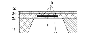
- the radiation source includes a substrate 13, a first insulating layer 22 formed on the substrate 13, a radiation surface layer 11 formed on the first insulation layer 22, and a second surface formed on the radiation surface layer 11.
- An insulating layer 24 and a plurality of extremely thin incandescent filaments 10 formed on the second insulating layer 24 are provided.
- the radiation source is formed so as to cover each incandescent filament 10, a third insulating layer 26 that protects each incandescent filament 10, and both ends of each incandescent filament 10 through openings formed in the third insulating layer 26.
- a pair of metal pads 15 and 15 connected to each other is provided.
- the second insulating layer 24 is provided to electrically insulate the radiating surface layer 11 from the incandescent filament 10.
- the incandescent filament 10 is surrounded by other elements (first insulating layer 22, radiation surface layer 11, second insulating layer 24, and third insulating layer 26) that form a multilayer structure as a uniform flat plate. It is stated that it is.
- Reference 1 describes that the purpose of providing the first insulating layer 22 and the third insulating layer 26 is to protect the incandescent filament 10 and the radiating surface layer 11 from oxidation.
- Document 1 describes an aqueous potassium hydroxide (KOH) solution, an ethylenediamine aqueous solution to which a small amount of pyrocatechol is added, and tetramethylammonium hydroxide (TMAH) as an etching solution that can be used to form the opening 14. .
- KOH potassium hydroxide
- TMAH tetramethylammonium hydroxide
- the substrate 13 is formed of a (100) oriented silicon chip.
- the first insulating layer 22 is made of a silicon nitride layer having a thickness of 200 nm.
- the radiation surface layer 11 is made of a polysilicon film having a thickness of about 1 ⁇ m and doped with boron, phosphorus or arsenic.
- the second insulating layer 24 is made of a silicon nitride layer having a thickness of about 50 nm.
- the incandescent filament 10 is made of a tungsten layer having a thickness of about 400 nm.
- the third insulating layer 26 is made of a silicon nitride layer having a thickness of about 200 nm.
- the metal pad 15 is made of, for example, aluminum, and forms ohmic contact with the incandescent filament 10 through an opening formed in the third insulating layer 26.
- the radiation surface layer 11 has an area of 1 mm 2 .
- the thickness is 0.1-1 ⁇ m
- the width is 2-10 ⁇ m
- the interval is 20-50 ⁇ m.
- the incandescent filament 10 is heated by the current flowing through the incandescent filament 10, the incandescent filament 10 is used exclusively for heating the radiating surface layer 11, and the radiating surface layer 11 is the main heat radiating source. Behave as.
- the infrared radiation element is intermittently driven to emit infrared light intermittently, and the output of the light receiving element that detects the infrared light is locked in. It is known that the S / N ratio of the output of the gas sensor can be improved by amplifying with an amplifier.
- the present invention has been made in view of the above reasons, and an object thereof is to provide an infrared radiation element capable of reducing power consumption and increasing response speed.
- a first form of an infrared radiation element includes a first insulating layer having thermal insulation and electrical insulation, a heating element layer formed on the first insulation layer and emitting infrared rays when energized, A second insulating layer formed on a side opposite to the first insulating layer with respect to the heating element layer and having thermal insulation and electrical insulation.
- the second insulating layer is configured to transmit infrared rays emitted from the heating element layer.
- the heating element layer has a sheet resistance selected such that the impedance of the heating element layer matches the impedance of the space in contact with the second insulating layer.
- the sheet resistance of the heating element layer is selected so that the infrared emissivity is not less than a specified value.
- the sheet resistance of the heating element layer is selected from a range of 73 ⁇ / ⁇ or more and 493 ⁇ / ⁇ or less.
- a fourth aspect of the infrared radiation element according to the present invention includes a substrate in any one of the first to third aspects.
- the first insulating layer is formed on one surface of the substrate.
- the substrate has an opening for exposing the first insulating layer.
- the heating element layer is disposed in a region where the first insulating layer and the opening are in contact with each other in plan view.
- a seventh aspect of the infrared radiation element according to the present invention is the both ends of the heating element layer on the opposite side to the first insulating layer with respect to the heating element layer in the fifth aspect or the sixth aspect.
- the pair of pads disposed in parallel to a predetermined direction in a region where the opening is not formed in a plan view, and the pair of pads A pair of electrical connection portions that electrically connect the pad to the pair of electrodes, respectively.
- the pair of electrical connection portions are arranged symmetrically with respect to a center line that passes through the center of gravity of the heating element layer and extends in the predetermined direction.
- each of the pair of electrical connection portions is composed of a plurality of wirings.
- the electrical connection portion is formed of tantalum.
- the heating element layer is formed of tantalum nitride or conductive polysilicon.
- (A) is a schematic plan view of the infrared radiation element of Embodiment 1, and (b) is a sectional view taken along line AA of (a).
- (A) is a schematic plan view of the infrared radiation element of Embodiment 2, and (b) is a sectional view taken along line AA of (a).
- (A) is a schematic plan view of the infrared radiation element of Embodiment 3, (b) is the sectional view on the AA line of (a).
- (A) is a schematic plan view of the infrared radiation element of Embodiment 4, (b) is the sectional view on the AA line of (a).
- FIG. 9 is a cross-sectional view taken along line A-A ′ of the radiation source in FIG. 8.
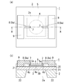
- Embodiment 1 Below, the infrared radiation element 1 of Embodiment 1 is demonstrated based on FIG.
- the infrared radiation element 1 of Embodiment 1 includes a substrate 2, a first insulating layer 3 formed on the one surface 21 side of the substrate 2, and a first side of the first insulating layer 3 opposite to the substrate 2 side. And a heating element layer 4 directly laminated on the insulating layer 3.
- the infrared radiation element 1 includes a pair of electrodes 7 and 7 formed so as to be in contact with the peripheral portion of the heating element layer 4 on the one surface 21 side of the substrate 2.
- the infrared radiation element 1 includes a pair of pads 9 and 9 electrically connected to each of the electrodes 7 and 7 via an electrical connection portion 8 (wiring 8a).
- the infrared radiation element 1 of the first embodiment is a second layer that is directly laminated on the heating element layer 4 on the side opposite to the substrate 2 side in the first insulating layer 3 and is transparent to infrared rays emitted from the heating element layer 4.
- An insulating layer 5 is provided.
- the substrate 2 has an opening 2a that exposes the surface of the first insulating layer 3 opposite to the heating element layer 4 side.
- infrared radiation element 1 are radiated from the heating element layer 4 by energizing the heating element layer 4.
- the infrared radiation element 1 includes the first insulating layer 3, the heating element layer 4 formed on the first insulating layer 3, and the heating element layer 4 opposite to the first insulating layer 3. And a second insulating layer 5 formed on the side.
- the heating element layer 4 generates heat and emits infrared rays when energized.
- the infrared radiation element 1 of Embodiment 1 includes a substrate 2, and the first insulating layer 3 is formed on one surface 21 of the substrate 2.
- the substrate 2 has an opening 2a through which the first insulating layer 3 is exposed.
- sheet resistance is set so as to suppress a decrease in the emissivity of infrared rays due to impedance mismatch with a space (for example, a gas such as air or nitrogen gas) in contact with the second insulating layer 5.
- a space for example, a gas such as air or nitrogen gas
- the substrate 2 is formed of a single crystal silicon substrate having a (100) plane on the one surface 21, but is not limited thereto, and may be formed of a single crystal silicon substrate having a (110) plane.
- the substrate 2 is not limited to a single crystal silicon substrate, but may be a polycrystalline silicon substrate or other than a silicon substrate.
- the material of the substrate 2 is preferably a material having a higher thermal conductivity and a larger heat capacity than the material of the first insulating layer 3.
- the outer peripheral shape of the substrate 2 is rectangular. That is, the substrate 2 has a rectangular shape in a plane orthogonal to the thickness direction of the substrate 2 (perpendicular direction in FIG. 1A; vertical direction in FIG. 1B). Although the external size of the board
- substrate 2 is not specifically limited, For example, it is preferable to set to 10 mm ⁇ or less (10 mm ⁇ 10 mm or less).
- the opening shape of the opening 2a of the substrate 2 is a rectangular shape.
- the opening 2a of the substrate 2 has an opening area on the other surface 22 side which is the surface opposite to the one surface 21 in the substrate 2 as compared with the one surface 21 (surface on the first insulating layer 3 side) side. It is formed in a larger shape.
- the opening 2 a of the substrate 2 is formed in a shape in which the opening area gradually increases as the distance from the first insulating layer 3 increases.
- the opening 2 a of the substrate 2 is formed by etching the substrate 2.
- the opening 2a of the substrate 2 can be formed by anisotropic etching using an alkaline solution as an etchant. it can.
- the opening shape of the opening 2a of the substrate 2 is not particularly limited.
- the mask layer at the time of forming the opening part 2a consists of an inorganic material at the time of manufacture, the mask layer may remain on the other surface 22 of the substrate 2.
- a laminated film of a silicon oxide film and a silicon nitride film can be employed.
- the first insulating layer 3 has thermal insulation and electrical insulation.
- the first insulating layer 3 is formed on one surface 21 of the substrate 2 so as to cover the opening 2a.
- the first insulating layer 3 includes a diaphragm portion 3D that separates the opening portion 2a and the heating element layer 4, and a support portion that is formed on the periphery of the opening portion 2a on the one surface 21 side of the substrate 2 and supports the diaphragm portion 3D. 3S. That is, the first insulating layer 3 includes a diaphragm portion 3D that is a portion located on the opening 2a on the one surface 21 of the substrate 2, and a support portion 3S that is a portion not located on the opening 2a.
- the diaphragm portion 3D is formed in the diaphragm region.
- the diaphragm region is a region where the opening 2a is formed on one surface 21 of the substrate 2 in plan view.
- the diaphragm region is a region where the opening 2a and the first insulating layer 3 (diaphragm portion 3D) are in contact with each other in plan view.
- in plan view refers to the case of viewing from the thickness direction of the substrate 2 (heating element layer 4).
- the infrared radiation element 1 includes a diaphragm body in the diaphragm region.
- the diaphragm body includes the first insulating layer 3 (diaphragm portion 3D), the heating element layer 4, the second insulating layer 5, the electrode 7, and the electrical connection portion 8.
- the first insulating layer 3 is formed so that the edge coincides with the substrate 2.
- the first insulating layer 3 includes a silicon oxide film on the substrate 2 side and a silicon nitride film stacked on the opposite side of the silicon oxide film from the substrate 2 side.
- the first insulating layer 3 is not limited to a laminated film of a silicon oxide film and a silicon nitride film, and may be a single layer structure of a silicon oxide film or a silicon nitride film, a single layer structure made of other materials, 2 A laminated structure of more than one layer may be used.
- the first insulating layer 3 is formed when the opening 2a is formed by etching the substrate 2 from the other surface 22 side of the substrate 2 which is the surface opposite to the one surface 21 of the substrate 2 when the infrared radiation element 1 is manufactured. It also has a function as an etching stopper layer.
- the heating element layer 4 is designed to generate heat and emit infrared rays when energized. That is, the heating element layer 4 functions as a heater and functions as a light emitting layer that emits infrared rays.
- the planar shape of the heating element layer 4 is rectangular. Here, the planar shape of the heating element layer 4 is defined as the shape of the heating element layer 4 in a plane orthogonal to the thickness direction of the heating element layer 4.
- the heating element layer 4 of Embodiment 1 is formed in a region (diaphragm region) where the first insulating layer 3 (diaphragm portion 3D) and the heating element layer 4 are in contact with each other in plan view.
- the heating element layer 4 is arranged in a region (diaphragm region) in which the opening 2a is formed on the one surface 21 side of the substrate 2 in plan view. In other words, the heating element layer 4 is located inside the opening 2 a in a plane parallel to the one surface 21 of the substrate 2.
- the planar size of the heating element layer 4 is preferably set smaller than the planar size of the surface of the first insulating layer 3 facing the opening 2a. That is, the planar size of the heating element layer 4 is preferably set smaller than the planar size of the diaphragm portion 3D (the size of the opening 2a on the one surface 21).
- the planar size of the diaphragm 3D is not particularly limited, but is preferably set to 5 mm ⁇ or less (5 mm ⁇ 5 mm or less), for example.
- the infrared radiation element 1 of Embodiment 1 includes an electrode 7, and the electrode 7 is in contact with the infrared radiation layer 4.
- a region in contact with each electrode 7 in the infrared radiation layer 4 is referred to as a contact region 4b.
- region except the contact region 4b among the heat generating body layers 4 is called the radiation
- the heating element layer 4 includes a pair of contact regions 4b so as to face each other.
- the contact region 4b is formed at the end of the surface of the heating element layer 4 opposite to the first insulating layer 3 (upper surface in FIG. 1B).
- the pair of contact regions 4b are formed at the end of the heating element layer 4 along the width direction of the heating element layer 4 (vertical direction in FIG. 1A; vertical direction in FIG. 1B). Yes.
- the planar size of the heating element layer 4 is set so that the planar size of the radiation area 4a excluding each contact area 4b where each electrode 7 overlaps the heating element layer 4 is 3 mm ⁇ or less (3 mm ⁇ 3 mm or less). Is preferred.
- the heating element layer 4 As a material for the heating element layer 4, tantalum nitride is employed. That is, the heating element layer 4 is made of a tantalum nitride layer made of tantalum nitride. The material of the heating element layer 4 is not limited to tantalum nitride.
- titanium nitride, nickel chromium, tungsten, titanium, thorium, platinum, zirconium, chromium, vanadium, rhodium, hafnium, ruthenium, boron, iridium, niobium, molybdenum Tantalum, osmium, rhenium, nickel, holmium, cobalt, erbium, yttrium, iron, scandium, thulium, palladium, lutetium, and the like may be employed.
- conductive polysilicon may be adopted as the material of the heating element layer 4.
- the heating element layer 4 may be composed of a conductive polysilicon layer made of polysilicon having conductivity.
- the heating element layer 4 it is preferable to employ a tantalum nitride layer or a conductive polysilicon layer from the viewpoint of chemical stability at high temperatures and ease of design of sheet resistance.
- the sheet resistance of the heating element layer 4 can be changed by changing the composition of the tantalum nitride layer (for example, the molar ratio of Ta and N).
- the heating element layer 4 is formed of a conductive polysilicon layer, the sheet resistance of the heating element layer 4 can be changed by changing the impurity concentration of the conductive polysilicon layer.
- the conductive polysilicon layer can be composed of an n-type polysilicon layer doped with an n-type impurity at a high concentration.
- the conductive polysilicon layer may be a p-type polysilicon layer doped with a high concentration of p-type impurities.
- the impurity concentration is, for example, 1 ⁇ 10 18 cm ⁇ 3 to 5 ⁇ 10 20 cm. What is necessary is just to set suitably in the range of about -3 .
- the impurity concentration is 1 ⁇ 10 18 cm ⁇ 3 to 1 ⁇ 10 20 cm. What is necessary is just to set suitably in the range of about -3 .
- a material of the heating element layer 4 from the viewpoint of preventing the heating element layer 4 from being destroyed due to thermal stress accompanying a difference in linear expansion coefficient between the substrate 2 and the heating element layer 4, A material having a small difference in linear expansion coefficient from the material is preferable.
- the infrared peak wavelength ⁇ emitted from the heating element layer 4 in the infrared radiation element 1 depends on the temperature of the heating element layer 4.
- the absolute temperature of the heating element layer 4 is T [K] and the peak wavelength is ⁇ [ ⁇ m]
- the infrared radiation element 1 can change Joule heat generated in the heating element layer 4 by adjusting input power applied between the pair of pads 9 and 9 from an external power source (not shown), for example.
- the temperature of the body layer 4 can be changed.
- the infrared radiation element 1 can change the temperature of the heating element layer 4 in accordance with the input power to the heating element layer 4, and can change the temperature of the heating element layer 4 from the heating element layer 4.
- the peak wavelength ⁇ of the emitted infrared light can be changed.
- the infrared radiation element 1 of Embodiment 1 it becomes possible to increase the amount of infrared radiation, so that the temperature of the heat generating body layer 4 is made high. For this reason, the infrared radiation element 1 can be used as a high-power infrared light source in a wide infrared wavelength range.
- the infrared radiation element 1 when used as an infrared light source of a gas sensor, it is possible to select a gas to be detected by the gas sensor by arbitrarily selecting an infrared frequency that is transmitted by an optical filter of a detector that receives infrared light. It becomes possible.
- the optical filter by designing the optical filter to transmit a plurality of infrared rays having different wavelengths, a gas sensor can detect a plurality of types of gases.
- the second insulating layer 5 has thermal insulation and electrical insulation.
- the second insulating layer 5 of the first embodiment is configured to transmit infrared rays emitted from the heating element layer 4.
- the second insulating layer 5 of Embodiment 1 is partially covered with the wiring 8a on the surface opposite to the heating element layer 4, and the other part is exposed and is in contact with the space.
- the second insulating layer 5 is composed of a silicon nitride film.
- the second insulating layer 5 is not limited to this.
- the second insulating layer 5 may be formed of a silicon oxide film, or may have a stacked structure of a silicon oxide film and a silicon nitride film.
- the second insulating layer 5 preferably has a high transmittance with respect to infrared rays of a desired wavelength or wavelength range radiated from the heating element layer 4 when the heating element layer 4 is energized, but it is essential that the transmittance is 100%. It is not something to do.
- the second insulating layer 5 of Embodiment 1 covers the heating element layer 4, and the heating element layer 4 is disposed between the second insulating layer 5 and the first insulating layer 3. Therefore, the second insulating layer 5 includes a pair of contact holes 5 a for bringing the electrode 7 into contact with the heating element layer 4.
- the contact hole 5a penetrates the second insulating layer 5, and the electrode 7 is formed on the heating element layer 4 through the contact hole 5a. Therefore, the electrode 7 can contact the heating element layer 4. That is, the heating element layer 4 can be energized through the electrode 7.
- the infrared radiation element 1 has a sandwich structure composed of a first insulating layer 3, a heating element layer 4 and a second insulating layer 5 (the heating element layer 4 is sandwiched between the first insulating layer 3 and the second insulating layer 5. It is preferable to set the materials and thicknesses of the first insulating layer 3 and the second insulating layer 5 in consideration of the stress balance of the structure. Thereby, the infrared radiation element 1 can improve the stress balance of the above-described sandwich structure, and can further suppress the warpage and breakage of the sandwich structure, thereby further improving the mechanical strength. Can be achieved.
- the thickness of the heating element layer 4 (the length in the vertical direction in FIG. 1A and the vertical length in FIG. 1B) is set.
- the thickness is preferably 0.2 ⁇ m or less.
- the total thickness of the thickness of the first insulating layer 3, the thickness of the heating element layer 4, and the thickness of the second insulating layer 5 is a laminated structure of the first insulating layer 3, the heating element layer 4, and the second insulating layer 5. From the standpoint of reducing the heat capacity, for example, it is preferably set in the range of about 0.1 ⁇ m to 1 ⁇ m, more preferably 0.7 ⁇ m or less.
- the pair of electrodes 7 and 7 is in contact with the peripheral portion (the left and right end portions in FIG. 1A) of the surface of the heating element layer 4 on the side opposite to the first insulating layer 2 on the one surface 21 side of the substrate 2. It is formed with. That is, the infrared radiation element 1 includes a pair of electrodes 7 and 7 respectively formed at both ends of the heating element layer 4 on the side opposite to the first insulating layer 3 with respect to the heating element layer 4. In the first embodiment, the pair of electrodes 7 and 7 are formed along the width direction of the heating element layer 4 (vertical direction in FIG. 1A, vertical direction in FIG. 1B), and the heating element layer 4 Are aligned in the length direction (the left-right direction in FIGS. 1A and 1B). Each electrode 7 is formed on the heating element layer 4 through a contact hole 5 a formed in the second insulating layer 5, and is electrically connected to the heating element layer 4. Here, each electrode 7 is in ohmic contact with the heating element layer 4.
- each electrode 7 is preferably formed of an aluminum alloy (Al—Si).
- the electrode 7 is preferably formed of Al or Al—Cu.
- the material of each electrode 7 is not particularly limited, and for example, gold or copper may be adopted.
- each electrode 7 should just be a material in which the part which contact
- each electrode 7 has a three-layer structure in which a first layer, a second layer, and a third layer are laminated in order from the heating element layer 4 side, and the material of the first layer in contact with the heating element layer 4 is a refractory metal.
- the second layer material may be nickel
- the third layer material may be gold.
- the pad 9 is formed on the support portion 3S. That is, the pad 9 is arranged in a region where the opening 2a is not formed in plan view. In other words, the pad 9 is disposed outside the opening 2 a in a plane parallel to the one surface 2 a of the substrate 2.
- the pair of pads 9 are arranged in parallel to each other in a region where the opening 2a is not formed in plan view. That is, the pair of pads 9 are arranged in parallel to the predetermined direction. In the first embodiment, the pair of pads 9 are arranged in parallel to each other across a region where the opening 2a is formed in plan view.
- the pair of electrical connection portions 8 and 8 electrically connect the pair of pads 9 and 9 to the pair of electrodes 7 and 7, respectively.
- the electrical connection portion 8 is composed of a single wiring 8a.
- Each electrical connection portion 8 (wiring 8a) and each pad 9 are preferably formed of the same material as each electrode 7 and set to the same layer structure and the same thickness. Thereby, in the infrared radiation element 1, each electrical connection portion 8 (wiring 8 a) and each pad 9 can be formed simultaneously with each electrode 7.
- the thickness of the pad 9 is preferably set in the range of about 0.5 to 2 ⁇ m.
- the first insulating layer 3, the heating element layer 4, and the second insulating layer 5 are sequentially formed on the one surface 21 side of the substrate 2, and then the second insulating layer 5 is formed. After forming the contact hole 5a, each electrode 7, each electrical connection portion 8 (wiring 8a) and each pad 9 are formed, and then the opening 2a is formed in the substrate 2.
- a method for forming the silicon oxide film of the first insulating layer 3 for example, a thin film forming technique such as a thermal oxidation method or a CVD (Chemical Vapor Deposition) method can be adopted, and a thermal oxidation method is preferable. Further, as a method for forming the silicon nitride film of the first insulating layer 3, a thin film forming technique such as a CVD method can be used, and an LPCVD (Low Pressure Chemical Vapor Deposition) method is preferable.
- LPCVD Low Pressure Chemical Vapor Deposition
- a method for forming the heating element layer 4 for example, a thin film forming technique such as a sputtering method, a vapor deposition method, or a CVD method, and a processing technique using a photolithography technique and an etching technique can be used.
- a thin film forming technique such as a sputtering method, a vapor deposition method, or a CVD method
- a processing technique using a photolithography technique and an etching technique can be used.
- a method for forming the second insulating layer 5 for example, a thin film forming technique such as a CVD method and a processing technique using a photolithography technique and an etching technique can be used.
- a CVD method for forming the second insulating layer 5 a plasma CVD method is preferable.
- a photolithography technique and an etching technique may be used.
- each electrode 7, each wiring 8 a and each pad 9 for example, a thin film forming technique such as a sputtering method, a vapor deposition method, and a CVD method, and a processing technique using a photolithography technique and an etching technique are used. be able to.
- a thin film forming technique such as a sputtering method, a vapor deposition method, and a CVD method
- a processing technique using a photolithography technique and an etching technique are used. be able to.
- a laminated film (not shown) of a silicon oxide film and a silicon nitride film is formed on the other surface 22 side of the substrate 2 which is the surface opposite to the one surface 21 of the substrate 2.
- the opening 2a may be formed by forming as a mask layer and etching the substrate 2 from the other surface 22 side.
- a silicon oxide film serving as a base of the mask layer is formed on the other surface 22 side of the substrate 2 simultaneously with the formation of the silicon oxide film of the first insulating layer 3 to form the first insulating layer.
- a silicon nitride film is formed on the other surface 22 side of the substrate 2 simultaneously with the formation of the silicon nitride film of the layer 3.
- the patterning of the laminated film of the silicon oxide film and the silicon nitride film that is the basis of the mask layer may be performed using a photolithography technique and an etching technique.
- the manufacturing method of the infrared radiation element 1 of Embodiment 1 it is possible to increase the accuracy of the thickness of the first insulating layer 3 by using the first insulating layer 3 as an etching stopper layer when forming the opening 2a. In addition, it is possible to prevent a part of the substrate 2 and residues from remaining on the opening 2a side of the first insulating layer 3. In this manufacturing method, it is possible to suppress variations in mechanical strength of the first insulating layer 3 and variations in heat capacity of the entire diaphragm portion 3D of the first insulating layer 3 for each infrared radiation element 1.
- the process until the formation of the opening 2a is completed at the wafer level, and after forming the opening 2a, the individual infrared radiation elements 1 may be separated. . That is, in manufacturing the plurality of infrared radiation elements 1, for example, a silicon wafer as a base of the substrate 2 is prepared, and the plurality of infrared detection elements 1 are formed on the silicon wafer according to the above-described manufacturing method. The infrared detecting element 1 may be separated.
- the infrared radiating element 1 can be manufactured by using a MEMS manufacturing technique.
- the heating element layer 4 is a sheet so as to suppress a decrease in the emissivity of infrared rays due to impedance mismatch with a space (for example, a gas such as air or nitrogen gas) in contact with the second insulating layer 5. Resistance is set. That is, the heating element layer 4 has a sheet resistance selected so that the impedance of the heating element layer 4 matches the impedance of the space in contact with the second insulating layer 5.
- the sheet resistance of the heating element layer 4 is determined by the nitrogen gas used when the tantalum nitride layer that forms the basis of the heating element layer 4 is formed by reactive sputtering. It is possible to control by partial pressure.
- the sheet resistance of the heating element layer 4 can be changed by changing the composition of the tantalum nitride layer (the ratio of Ta and N).
- the sheet resistance of the heating element layer 4 is changed by changing the impurity concentration of the conductive polysilicon layer that is the basis of the heating element layer 4.
- a method for controlling the impurity concentration of the conductive polysilicon layer there are a method of doping impurities after forming a non-doped polysilicon layer, a method of doping impurities during film formation, and the like.
- the above-mentioned space (gas) is air
- tantalum nitride is adopted as the material of the heating element layer 4
- the heating element layer 4 is heated to, for example, 500 ° C. as a desired use temperature.
- the sheet resistance of the heating element layer 4 at which the emissivity of infrared rays from the heating element layer 4 becomes maximum at this operating temperature is 189 ⁇ / ⁇ (189 ⁇ / sq.), And the maximum value of the emissivity is 50%. That is, if the sheet resistance of the heating element layer 4 is 189 ⁇ / ⁇ , the infrared radiation element 1 can maximize the infrared emissivity by impedance matching with air.
- the sheet resistance of the heating element layer 4 may be set in the range of 73 to 493 ⁇ / ⁇ . If the sheet resistance at which the emissivity is maximized at a desired use temperature is referred to as a prescribed sheet resistance, the sheet resistance of the heating element layer 4 at the desired use temperature is within a range of the prescribed sheet resistance ⁇ 10%. It is more preferable to set. That is, in the infrared radiation element 1, the sheet resistance of the heating element layer 4 is preferably selected such that the infrared emissivity is equal to or higher than a specified value. Specifically, the sheet resistance of the heating element layer 4 is preferably selected from a range of 73 ⁇ / ⁇ or more and 493 ⁇ / ⁇ or less.
- the infrared radiation element 1 includes a substrate 2, a first insulating layer 3, a heating element layer 4, a second insulating layer 5, and a pair of electrodes 7 and 7.
- An infrared ray is emitted from the layer 4, and an opening 2 a that exposes the surface of the first insulating layer 3 opposite to the heating element layer 4 side is formed in the substrate 2.
- the sheet resistance is set so as to suppress a decrease in infrared emissivity due to impedance mismatch with the space (gas) in contact with the two insulating layers 5.
- the infrared radiation element 1 of Embodiment 1 has the following first to seventh and eleventh characteristics. The eighth to tenth features will be described later.
- the infrared radiation element 1 includes a first insulating layer 3 having thermal insulation and electrical insulation, a heating element layer 4 formed on the first insulation layer 3 and emitting infrared rays when energized,
- the heating element layer 4 includes a second insulating layer 5 formed on the opposite side of the first insulating layer 3 and having thermal insulation and electrical insulation.
- the second insulating layer 5 is configured to transmit infrared rays emitted from the heating element layer 4.
- the heating element layer 4 has a sheet resistance selected so that the impedance of the heating element layer 4 matches the impedance of the space in contact with the second insulating layer 5.
- the sheet resistance of the heating element layer 4 is selected so that the infrared emissivity is equal to or higher than a specified value.
- the second feature is an arbitrary feature.
- the sheet resistance of the heating element layer 4 is selected from a range of 73 ⁇ / ⁇ or more and 493 ⁇ / ⁇ or less.
- the third feature is an arbitrary feature.
- the infrared radiating element 1 in the fourth feature, in the infrared radiating element 1 having any one of the first to third features, the infrared radiating element 1 includes a substrate 2.
- the first insulating layer 3 is formed on the one surface 21 of the substrate 2.
- the 4th characteristic is arbitrary characteristics.
- the substrate 2 has an opening 2a through which the first insulating layer 3 is exposed.
- the fifth feature is an optional feature.
- the heating element layer 4 is disposed in a region where the first insulating layer 3 and the opening 2a are in contact with each other in plan view.
- the sixth feature is an arbitrary feature in the infrared radiation element 1 of the present embodiment.
- the infrared radiation element 1 in the infrared radiation element 1 having the fifth or sixth feature, the infrared radiation element 1 is disposed at both ends of the heating element layer 4 on the side opposite to the first insulating layer 3 with respect to the heating element layer 4. A pair of electrodes 7, 7 formed respectively on the part is provided.
- the seventh feature is an arbitrary feature.
- the infrared radiation element 1 having the first, fourth, fifth, and seventh features, the infrared radiation element 1 is formed on the substrate 2 and the first surface 21 side of the substrate 2. Insulating layer 3, heating element layer 4 directly laminated on the side opposite to substrate 2 side in first insulating layer 3, and in contact with the peripheral portion of heating element layer 4 on the one surface 21 side of substrate 2 A pair of formed electrodes 7 and 7 and a second insulating layer that is directly laminated on the heating element layer 4 on the side opposite to the substrate 2 side in the first insulating layer 3 and is transparent to infrared rays emitted from the heating element layer 4 Layer 5.
- the substrate 2 is formed with an opening 2a that exposes the surface of the first insulating layer 3 opposite to the heating element layer 4 side.
- the heating element layer 4 is set to have a sheet resistance so as to suppress a decrease in infrared emissivity due to impedance mismatch with the gas in contact with the second insulating layer 5.
- the heating element layer 4 is made of a tantalum nitride layer or a conductive polysilicon layer.
- the eleventh feature is an arbitrary feature.
- the heating element layer 4 is formed of tantalum nitride or polysilicon having conductivity.
- the infrared output of the infrared emitting element is substantially proportional to the infrared emissivity of the layer that emits infrared rays (the heating element layer 4 in the first embodiment).
- the infrared emissivity is approximately proportional to the fourth power of the temperature of an object that emits infrared rays (the heating element layer 4 in the first embodiment).
- the temperature of the heating element layer 4 is proportional to the amount of heat (electric power) input to the heating element layer 4 and inversely proportional to the heat capacity of the heating element layer 4, the first insulating layer 3, and the second insulating layer 5.
- the heat capacity of the layer is proportional to the thickness of the layer per unit area.
- the thickness of the radiation surface layer is about 1 ⁇ m.
- the heat capacity of the radiation surface layer is increased, so that the infrared output may be smaller than that of the infrared radiation element having a thin radiation surface layer.
- a thick radiating surface layer requires more power to reach the same temperature than a thin radiating surface layer (here, a thick radiating surface layer and a thin radiating surface layer have conditions other than thickness) The same). Therefore, even if the same power is applied to the thick radiating surface layer and the thin radiating surface layer, the temperature rise of the thick radiating surface layer is smaller than that of the thin radiating surface layer. Therefore, the infrared emissivity of the thick radiating surface layer may be smaller than that of the thin radiating surface layer.
- the infrared radiation element 1 of Embodiment 1 is configured so that the impedance of the heating element layer 4 and the impedance of the space in contact with the second insulating layer 5 are matched in order to improve the infrared output. Therefore, in the infrared radiation element 1, even when the thickness of the infrared radiation layer (heating element layer 4) is thinner than the conventional infrared radiation element (for example, 0.2 ⁇ m), the heating element layer 4 has a relatively large infrared ray. It has an emissivity (about 50%).
- the heat capacity of the heat generating layer 4 is not increased (the thickness is increased). Without), the emissivity of infrared rays can be increased, and the output of the infrared radiation element 1 can be increased.
- the thermal time constant of an object is generally proportional to the heat capacity of the object. Therefore, in the conventional infrared radiation element in which the infrared radiation layer (radiation surface layer) is thickened, the heat capacity of the radiation surface layer increases and the thermal time constant also increases. That is, it is difficult to increase the response speed with the conventional infrared radiation element.
- the infrared radiation element 1 with high output without increasing the heat capacity of the heat generation element layer 4, that is, the heating element layer 4 of the infrared radiation element 1 with high output.
- the thermal time constant can be reduced. Therefore, it is possible to increase the output of the infrared radiation element 1 and increase the response speed of the infrared radiation element 1.
- the infrared radiation element 1 according to the first embodiment can achieve both low power consumption and high response speed. That is, in the infrared radiation element 1 of Embodiment 1, it is possible to reduce power consumption and increase response speed.
- the infrared radiation element 1 reduces the heat capacity of the laminated structure (here, the first insulating layer 3, the heating element layer 4, and the second insulating layer 5) formed on the one surface 21 side of the substrate 2. In addition, it is possible to suppress a decrease in the emissivity of the heating element layer 4. Therefore, in the infrared radiation element 1 of Embodiment 1, it becomes possible to reduce power consumption and increase the response speed. In addition, the infrared radiation element 1 speeds up the response of the temperature change of the heating element layer 4 to the voltage waveform applied between the pair of pads 9 by reducing the heat capacity of the laminated structure on the one surface 21 side of the substrate 2. Thus, the temperature of the heating element layer 4 is likely to rise, and it becomes possible to increase the output and increase the response speed.
- the substrate 2 is formed from a single crystal silicon substrate, and the first insulating layer 3 is composed of a silicon oxide film and a silicon nitride film. Accordingly, the infrared radiation element 1 has a larger heat capacity and thermal conductivity of the substrate 2 than the first insulating layer 3, and the substrate 2 has a function as a heat sink. Therefore, the infrared radiation element 1 is reduced in size and has a high response speed to input power. And stability of infrared radiation characteristics can be improved.
- the infrared radiation element 1 tantalum nitride having a melting point higher than that of silicon is adopted as the material of the heating element layer 4. Therefore, a member (in the first embodiment, the first insulating layer 3, the second insulating layer 5, the electrode 7, and the electrical connection portion 8) that is not the heating element layer 4 constituting the diaphragm body has a higher melting point than the heating element layer 4. If so, it becomes possible to raise the temperature of the heating element layer 4 to the maximum use temperature of the silicon constituting the substrate 2 (a temperature slightly lower than the melting point of silicon), and the amount of infrared radiation compared to the infrared light emitting diode. Can be significantly increased.
- the temperature of the heating element layer 4 is restricted by the material of each electrode 7 as long as at least a portion in contact with the heating element layer 4 is formed of a metal having a melting point higher than that of silicon. It is possible to raise without having to.
- the temperature of the heating element layer 4 is slightly lower than the melting point of the heating element layer 4. Can be raised.
- the temperature of the heating element layer 4 refers to the temperature near the center (near the center of gravity) of the heating element layer 4.
- the heating element layer 4 is formed of a high melting point material (a material having a high melting point) such as tantalum nitride
- the other members constituting the diaphragm body first insulating layer 3, second insulating layer 5, electrode 7, The connecting portion 8) can be formed from the following high melting point material.
- the high melting point material used for the first insulating layer 3 and the second insulating layer 5 is, for example, an insulator (silicon dioxide, silicon nitride) having a high melting point.
- the high melting point material used for the electrode 7 and the electrical connection part 8 (wiring 8a) is, for example, a metal having a high melting point (tantalum, tungsten, molybdenum, etc.), a noble metal having a high melting point (platinum, ruthenium, iridium, etc.), and , A conductive material having a high melting point (conductive single crystal silicon, conductive polysilicon, conductive single crystal germanium, conductive polygermanium, conductive carbon).
- the electrical connection portion 8 is made of tantalum (Ta).
- the electrical connection portion 8 is formed of a noble metal having a high melting point as described above, even when the electrical connection portion 8 is exposed and formed, when the temperature of the heating element layer 4 is increased, It is possible to suppress the electrical resistance from changing due to oxidation of the electrical connection portion 8.
- the high melting point material may be a material having a higher melting point than the material forming the substrate 2.
- the high melting point material is selected from materials having a melting point higher than that of silicon.
- the temperature of the heating element layer 4 (heating element) The temperature near the center of the layer 4) can be raised to a temperature slightly lower than the melting point of the material having the lowest melting point among the members constituting the diaphragm body.
- the heating element layer 4 is more likely to dissipate heat as it is closer to the periphery of the heating element layer 4.
- the heating element layer 4 is more likely to dissipate heat as it is closer to the substrate 2. Therefore, the temperature of the peripheral portion of the heating element layer 4 is lower than the temperature at the center of the heating element layer 4.
- the electrical connection portion 8 that is in contact with the peripheral portion of the heating element layer 4 has substantially the same temperature as the peripheral portion of the heating element layer 4 at or near the portion that is in contact with the heating element layer 4.
- the temperature of the peripheral portion of the heating element layer 4 is slightly lower than the temperature near the center of the heating element layer 4, the temperature near the center of the heating element layer 4 is changed to the material constituting the diaphragm body.
- the infrared radiation element 1 can be used stably.
- the infrared radiation element 1 of Embodiment 1 has the following tenth feature in addition to the first to seventh and eleventh features.
- the electrical connection portion 8 is formed of tantalum.
- the tenth feature is an optional feature.
- the heating element layer 4, the electrode 7, the wiring 8 a and the pad 9 are viewed from a plan view (thickness direction (perpendicular to the paper surface of FIG. 1A; vertical direction of FIG. 1B)).
- the center line of the infrared radiation element 1 orthogonal to the direction in which the pair of electrodes 7 and 7 are arranged is preferably arranged symmetrically about the axis of symmetry. That is, the structure of the surface on which the heating element layer 4 is formed in the infrared radiation element 1 is the length direction of the infrared radiation element 1 passing through the center of the infrared radiation element 1 in plan view (up and down in FIG. 1A).
- the pair of electrical connection portions 8 are arranged symmetrically with respect to the center line.
- the center line is a line that passes through the center of gravity of the heating element layer 4 and extends in the predetermined direction.
- the pair of pads 9 are arranged in parallel with the predetermined direction.
- the infrared radiation element 1 can further improve the mechanical strength, and can suppress the in-plane variation of the temperature of the heating element layer 4.
- not only the pair of electrical connection portions 8 but also the heating element layer 4 and the electrode 7 are arranged symmetrically with respect to the center line.
- the structure of the infrared radiation element 1 is two-fold symmetric with an imaginary line passing through the center of the surface on which the heating element layer 4 is formed and along the thickness direction of the infrared radiation element 1 as a rotation axis. .
- the infrared radiation element 1 according to Embodiment 1 has the eighth feature in addition to the first to seventh, tenth, and eleventh features.
- the infrared radiation element 1 includes a pair of pads 9 arranged in parallel to the predetermined direction in a region where the opening 2a is not formed, and the pair of pads 9 as a pair of electrodes 7 in a plan view.
- a pair of electrical connection portions 8 that are electrically connected to each other.
- the pair of electrical connection portions 8 are arranged symmetrically with respect to a center line that passes through the center of gravity of the heating element layer 4 and extends in the predetermined direction.
- the 8th characteristic is arbitrary characteristics.
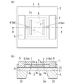
- Embodiment 2 Below, the infrared radiation element 1 of Embodiment 2 is demonstrated based on FIG.
- the infrared radiation element 1 according to the second embodiment has the first to eighth, tenth, and eleventh features as described above, similarly to the infrared radiation element 1 according to the first embodiment.
- the infrared radiation element 1 of Embodiment 2 makes the 2nd insulating layer 5 the thickness direction of the diaphragm part 3D in the 1st insulating layer 3 (paper surface perpendicular
- the infrared radiation element according to the second embodiment is different from the infrared radiation element 1 according to the first embodiment in a region where the second insulating layer 5 is formed.
- the second insulating layer 5 is formed only in the diaphragm region in which the opening 2a is provided on the one surface 21 in plan view.
- symbol is attached
- the infrared radiation element 1 of the second embodiment has a laminated structure (the first insulating layer 3, the heating element layer 4, and the second structure) formed on the one surface 21 side of the substrate 2. It is possible to reduce the heat capacity of the insulating layer 5), and to further reduce power consumption.
- Embodiment 3 Below, the infrared radiation element 1 of Embodiment 3 is demonstrated based on FIG.
- the infrared radiating element 1 of the third embodiment has the first to eighth, tenth and eleventh features as in the infrared radiating element 1 of the first embodiment.
- the infrared radiation element 1 of Embodiment 3 differs from the infrared radiation element 1 of Embodiment 1 in the point by which the one electrical connection part 8 is comprised by the some wiring 8a. That is, the infrared radiation element 1 according to Embodiment 3 has the ninth feature described below in addition to the first to eighth, tenth, and eleventh features.
- the infrared radiation element 1 according to the third embodiment is different from the infrared radiation element 1 according to the first embodiment in that the electrical connection portion 8 that connects the electrode 7 and the pad 9 has two wirings 8a.
- symbol is attached
- the electrical connection portion 8 for connecting the electrode 7 and the pad 9 is composed of two wirings 8a and 8a.
- the wiring 8a is in a direction orthogonal to the juxtaposed direction of the pair of pads 9 and 9 in a plan view (when viewed from the vertical direction in FIG. 3A; viewed from the up and down direction in FIG. 3B).
- the heating element layer 4 is connected to both ends. That is, the wiring 8a is in contact with the end of the electrode 7 and is arranged in a shape extending in the width direction of the infrared radiation element 1 (left and right direction in FIGS. 3A and 3B).
- the infrared radiation element 1 of Embodiment 3 has one wiring 8a connected to the central portion of the heating element layer 4 in the direction orthogonal to the parallel arrangement direction like the infrared radiation element 1 of Embodiment 1. Compared to the case, it is possible to make the current density of the current flowing through the heating element layer 4 uniform.
- the diaphragm portion 3D is deformed with expansion and contraction due to the heat generation of the heating element layer 4, and mechanical stress may be applied to the electrical connection portion 8 (wiring 8a) and the like. Since the infrared radiation element 1 of Embodiment 3 includes two wirings 8a that connect the electrodes 7 and the pads 9, even if one of the two wirings 8a is disconnected, it can be used. Therefore, it is possible to improve the reliability and extend the life.
- the electrical connection unit 8 is configured by two wirings 8a. However, the electrical connection unit 8 may be configured by three or more wirings 8a.
- the infrared radiation element 1 of Embodiment 3 has the ninth feature in addition to the first to eighth, tenth, and eleventh features.
- each of the pair of electrical connection portions 8 includes a plurality of wirings 8a.
- the 2nd, 3rd, 10th, and 11th characteristics are arbitrary characteristics.
- two wirings 8a for connecting the electrode 7 and the pad 9 may be provided.
- Embodiment 4 Below, the infrared radiation element 1 of Embodiment 4 is demonstrated based on FIG.
- the infrared radiating element 1 of the fourth embodiment has the first to eighth, tenth, and eleventh features as in the infrared radiating element 1 of the first embodiment.
- the infrared radiation element 1 of Embodiment 4 is orthogonal to the planar shape of the heating element layer 4 (the thickness direction of the heating element layer 4 (the direction perpendicular to the paper surface in FIG. 4A; the vertical direction in FIG. 4B)). The point that the shape of the heating element layer 4 in the plane is circular is different from the infrared radiation element 1 of the first embodiment.
- symbol is attached
- the temperature variation of the heating element layer 4 is reduced as compared with the case where the planar shape of the heating element layer 4 is rectangular as in the infrared radiation element 1 of the first embodiment.
- the infrared radiation element 1 of Embodiment 4 can achieve low power consumption.
- the planar shape of the heating element layer 4 may be circular.
- Embodiment 5 Below, the infrared radiation element 1 of Embodiment 5 is demonstrated based on FIG.
- the infrared radiation element 1 of the fifth embodiment has the above-described first to eighth, tenth, and eleventh features, similar to the infrared radiation element 1 of the first embodiment.
- the infrared radiation element 1 of Embodiment 5 is orthogonal to the planar shape of the heating element layer 4 (thickness direction of the heating element layer 4 (perpendicular to the paper surface in FIG. 5A; up and down direction in FIG. 5B)).
- the shape of the heating element layer 4 in the plane is different from the infrared radiation elements 1 of the first to fourth embodiments.
- symbol is attached
- the planar shape of the heating element layer 4 in the infrared radiation element 1 of Embodiment 5 is such that the width dimension of the heating element layer 4 increases as the distance from each electrode 7 increases in the direction in which the pair of electrodes 7 and 7 are arranged side by side. The direction dimension) is gradually reduced.
- the variation in temperature of the heating element layer 4 is reduced as compared to the case where the planar shape of the heating element layer 4 is rectangular as in the infrared radiation element 1 of the first embodiment.
- the infrared radiation element 1 of Embodiment 5 can achieve low power consumption.
- Embodiment 6 Below, the infrared radiation element 1 of Embodiment 6 is demonstrated based on FIG.
- the infrared radiation element 1 of the sixth embodiment has the above first to eighth, tenth, and eleventh features, similar to the infrared radiation element 1 of the first embodiment.
- the infrared radiation element 1 according to the sixth embodiment has a plurality (see FIG. 6A) that communicates with the opening 2a of the substrate 2 in a region where the diaphragm portion 3D and the second insulating layer 5 of the first insulating layer 3 are stacked. ) Is different from the infrared radiation element 1 of the first embodiment in that six through holes 3H are formed. That is, in the sixth embodiment, the through hole 3H is formed in a region where the heating element layer 4 is not formed in the diaphragm region in plan view.
- the through hole 3H is formed in the diaphragm region where the heating element layer 4 is not formed and the first insulating layer 3 and the second insulating layer 5 are formed. That is, the through hole 3H does not penetrate the heating element layer 4 but penetrates the first insulating layer 3 and the second insulating layer 5 on the opening 2a.
- symbol is attached
- the plurality of through holes 3H are disposed so as to surround the heating element layer 4 in a plan view (when viewed from the direction perpendicular to the paper surface in FIG. 6A; viewed from the up and down direction in FIG. 6B).
- the opening shape of each through-hole 3H in plan view is an oval shape, but is not limited thereto, and may be a circular shape, for example.
- each through hole 3H has an oval opening shape arranged along one side of the outer periphery of the rectangular heating element layer 4 in plan view.
- the present invention is not limited to this, and an L-shaped opening shape disposed along two sides or a U-shaped opening shape disposed along three sides may be employed.
- the plurality of through holes 3H are preferably arranged in line symmetry with the center line of the infrared radiation element 1 orthogonal to the direction in which the pair of electrodes 7 and 7 are arranged in plan view as the axis of symmetry.
- the infrared radiating element 1 of the sixth embodiment since the plurality of through holes 3H described above are formed, it is possible to reduce the thermal conductance between the heating element layer 4 and the substrate 2 and to further reduce the thermal conductivity. It is possible to reduce power consumption.
- the infrared radiation element 1 of Embodiment 6 it is orthogonal to the planar shape of the heating element layer 4 (thickness direction of the heating element layer 4 (perpendicular to the plane of the paper in FIG. 6A; up and down direction in FIG. 6B)).
- the shape of the heating element layer 4 in the plane to be formed may be the same as that of each of the fourth and fifth embodiments.
- Embodiment 7 Below, the infrared radiation element 1 of Embodiment 7 is demonstrated based on FIG.
- the infrared radiation element 1 according to the seventh embodiment has the first to eighth, tenth, and eleventh features as described above, similarly to the infrared radiation element 1 according to the first embodiment.
- the laminated structure portion of the first insulating layer 3, the heating element layer 4, and the second insulating layer 5 on the opening 2a of the substrate 2 is connected via the wirings 8a and 8a.
- the infrared radiation element 1 of the first embodiment is different from the infrared radiation element 1 of the first embodiment in that it is supported by the support portion 3S of the first insulating layer 3.
- symbol is attached
- a slit 6 that surrounds the entire circumference of the above-described laminated structure portion is formed in a laminated film of the first insulating layer 3 and the second insulating layer 5.
- the slit 6 communicates with the opening 2a.
- the infrared radiation element 1 according to the seventh embodiment can reduce the thermal conductance between the heating element layer 4 and the substrate 2 as compared with the first embodiment, and can further reduce the power consumption. It becomes.
- the infrared radiation element 1 of Embodiment 7 it is orthogonal to the planar shape of the heating element layer 4 (thickness direction of the heating element layer 4 (perpendicular to the paper surface in FIG. 7A; up and down direction in FIG. 7B)).
- the shape of the heating element layer 4 in the plane to be formed may be the same as that of each of the fourth and fifth embodiments.
- the infrared radiation element 1 of each embodiment is not limited to an infrared light source for a gas sensor, but can be used for an infrared light source for infrared light communication, an infrared light source for spectral analysis, and the like.
Abstract
Description
製造される赤外線放射素子が研究開発されている。この種の赤外線放射素子は、ガスセンサや光学分析装置などの赤外線源として使用することができる。 2. Description of the Related Art Conventionally, an infrared emitting element manufactured using a manufacturing technology of MEMS (micro electro mechanical systems) has been researched and developed. This type of infrared radiation element can be used as an infrared source such as a gas sensor or an optical analyzer.
本発明に係る赤外線放射素子の第6の形態では、前記第5の形態において、前記発熱体層は、平面視において、前記第1絶縁層と前記開口部とが接する領域に配置される。 In a fifth aspect of the infrared radiation element according to the present invention, in the fourth aspect, the substrate has an opening for exposing the first insulating layer.
In a sixth aspect of the infrared radiation element according to the present invention, in the fifth aspect, the heating element layer is disposed in a region where the first insulating layer and the opening are in contact with each other in plan view.
以下では、実施形態1の赤外線放射素子1について図1に基づいて説明する。 (Embodiment 1)
Below, the
λ=2898/T
となり、発熱体層4の絶対温度Tと発熱体層4から放射される赤外線のピーク波長λとの関係がウィーンの変位則を満足している。赤外線放射素子1は、例えば、外部電源(図示せず)から一対のパッド9,9間に与える入力電力を調整することにより、発熱体層4に発生するジュール熱を変化させることができ、発熱体層4の温度を変化させることができる。つまり、発熱体層4の温度は、発熱体層4に与える電力に応じて、変化する。したがって、赤外線放射素子1は、発熱体層4への入力電力に応じて発熱体層4の温度を変化させることができ、また、発熱体層4の温度を変化させることで発熱体層4から放射される赤外線のピーク波長λを変化させることができる。また、実施形態1の赤外線放射素子1では、発熱体層4の温度を高くするほど赤外線の放射量を増大させることが可能となる。このため、赤外線放射素子1を、広範囲の赤外線波長域において高出力の赤外線光源として用いることが可能となる。例えば、赤外線放射素子1をガスセンサの赤外光源として使用する場合には、赤外線を受光するディテクタの光学フィルタで透過させる赤外線の周波数を任意に選ぶことにより、ガスセンサが検知するガスを選択することが可能となる。特に、光学フィルタを波長が異なる複数の赤外線を透過させるように設計することにより、ガスセンサで複数種類のガスを検知できる。 The infrared peak wavelength λ emitted from the
λ = 2898 / T
Thus, the relationship between the absolute temperature T of the
み方向(図1(a)の紙面垂直方向;図1(b)の上下方向)から見た場合)において一対の電極7,7の並ぶ方向に直交する赤外線放射素子1の中心線を対称軸として線対称に配置されていることが好ましい。つまり、赤外線放射素子1における発熱体層4が形成された側の面の構造は、平面視において、赤外線放射素子1の中心を通る赤外線放射素子1の長さ方向(図1(a)の上下方向、図1(b)の紙面垂直方向)の仮想線を対称軸として線対称である。さらに換言すれば、一対の電気接続部8は、中心線に対して線対称に配置される。前記中心線とは、発熱体層4の重心を通り前記所定方向に伸びる線である。一対のパッド9は、前記所定方向と平行に配置されている。これにより、赤外線放射素子1は、機械的強度のより一層の向上を図ることが可能となるとともに、発熱体層4の温度の面内ばらつきを抑制することが可能となる。本実施形態では、一対の電気接続部8だけでなく、発熱体層4、電極7も、前記中心線に対して線対称に配置される。換言すれば、赤外線放射素子1の構造は、発熱体層4が形成された側の面の面心を通り赤外線放射素子1の厚み方向に沿った仮想線を回転軸として、2回対称である。 In the
以下では、実施形態2の赤外線放射素子1について図2に基づいて説明する。 (Embodiment 2)
Below, the
以下では、実施形態3の赤外線放射素子1について図3に基づいて説明する。 (Embodiment 3)
Below, the
以下では、実施形態4の赤外線放射素子1について図4に基づいて説明する。 (Embodiment 4)
Below, the
以下では、実施形態5の赤外線放射素子1について図5に基づいて説明する。 (Embodiment 5)
Below, the
以下では、実施形態6の赤外線放射素子1について図6に基づいて説明する。 (Embodiment 6)
Below, the
以下では、実施形態7の赤外線放射素子1について図7に基づいて説明する。 (Embodiment 7)
Below, the
Claims (11)
- 熱絶縁性および電気絶縁性を有する第1絶縁層と、
前記第1絶縁層上に形成され、通電により赤外線を放射する発熱体層と、
前記発熱体層に対して前記第1絶縁層とは反対側に形成され、熱絶縁性および電気絶縁性を有する第2絶縁層と、
を備え、
前記第2絶縁層は、前記発熱体層から放射される赤外線を透過するように構成され、
前記発熱体層は、前記発熱体層のインピーダンスが前記第2絶縁層の接触する空間のインピーダンスと整合するように選択されたシート抵抗を有する
ことを特徴とする赤外線放射素子。 A first insulating layer having thermal insulation and electrical insulation;
A heating element layer formed on the first insulating layer and emitting infrared rays when energized;
A second insulating layer formed on a side opposite to the first insulating layer with respect to the heating element layer, and having thermal insulation and electrical insulation;
With
The second insulating layer is configured to transmit infrared rays emitted from the heating element layer,
The infrared radiation element, wherein the heating element layer has a sheet resistance selected so that an impedance of the heating element layer matches an impedance of a space in contact with the second insulating layer. - 前記発熱体層のシート抵抗は、赤外線の放射率が規定値以上となるように選択される
ことを特徴とする請求項1に記載の赤外線放射素子。 The infrared radiation element according to claim 1, wherein the sheet resistance of the heating element layer is selected so that an infrared emissivity is equal to or higher than a specified value. - 前記発熱体層のシート抵抗は、73Ω/□以上493Ω/□以下の範囲から選択される
ことを特徴とする請求項2に記載の赤外線放射素子。 The infrared radiation element according to claim 2, wherein the sheet resistance of the heating element layer is selected from a range of 73Ω / □ or more and 493Ω / □ or less. - 基板を備え、
前記第1絶縁層は、前記基板の一表面上に形成される
ことを特徴とする請求項1~3のいずれか1項に記載の赤外線放射素子。 Equipped with a substrate,
The infrared radiation element according to any one of claims 1 to 3, wherein the first insulating layer is formed on one surface of the substrate. - 前記基板は、前記第1絶縁層を露出させる開口部を有する
ことを特徴とする請求項4に記載の赤外線放射素子。 The infrared radiation element according to claim 4, wherein the substrate has an opening that exposes the first insulating layer. - 前記発熱体層は、平面視において、前記第1絶縁層と前記開口部とが接する領域に配置される
ことを特徴とする請求項5に記載の赤外線放射素子。 The infrared radiation element according to claim 5, wherein the heating element layer is disposed in a region where the first insulating layer and the opening are in contact with each other in plan view. - 前記発熱体層に対して前記第1絶縁層とは反対側における前記発熱体層の両端部にそれぞれ形成される一対の電極を備える
ことを特徴とする請求項5又は6に記載の赤外線放射素子。 The infrared radiation element according to claim 5 or 6, comprising a pair of electrodes respectively formed at both ends of the heating element layer on a side opposite to the first insulating layer with respect to the heating element layer. . - 平面視において、前記開口部が形成されていない領域に配置される一対のパッドと、
前記一対のパッドを前記一対の電極にそれぞれ電気的に接続する一対の電気接続部と、
を備え、
前記一対のパッドは、所定方向に平行に配置され、
前記一対の電気接続部は、前記発熱体層の重心を通り前記所定方向に伸びる中心線に対して、線対称に配置される
ことを特徴とする請求項7に記載の赤外線放射素子。 In plan view, a pair of pads arranged in a region where the opening is not formed,
A pair of electrical connections for electrically connecting the pair of pads to the pair of electrodes, respectively.
With
The pair of pads are arranged in parallel to a predetermined direction,
The infrared radiation element according to claim 7, wherein the pair of electrical connection portions are arranged symmetrically with respect to a center line extending in the predetermined direction through the center of gravity of the heating element layer. - 前記一対の電気接続部のそれぞれは、複数の配線で構成される
ことを特徴とする請求項8に記載の赤外線放射素子。 The infrared radiation element according to claim 8, wherein each of the pair of electrical connection portions includes a plurality of wirings. - 前記電気接続部は、タンタルで形成される
ことを特徴とする請求項8又は9に記載の赤外線放射素子。 The infrared radiation element according to claim 8, wherein the electrical connection portion is made of tantalum. - 前記発熱体層は、窒化タンタルまたは導電性を有するポリシリコンで形成される
ことを特徴とする請求項1~10のいずれか1項に記載の赤外線放射素子。 11. The infrared radiation element according to claim 1, wherein the heating element layer is made of tantalum nitride or conductive polysilicon.
Priority Applications (4)
| Application Number | Priority Date | Filing Date | Title |
|---|---|---|---|
| US14/398,205 US9105368B2 (en) | 2012-05-09 | 2013-03-12 | Infrared radiation element |
| CN201380024319.1A CN104272086B (en) | 2012-05-09 | 2013-03-12 | Infrared radiation element |
| JP2014514356A JP5895205B2 (en) | 2012-05-09 | 2013-03-12 | Infrared radiation element |
| EP13787333.7A EP2848914A4 (en) | 2012-05-09 | 2013-03-12 | Infrared radiation element |
Applications Claiming Priority (2)
| Application Number | Priority Date | Filing Date | Title |
|---|---|---|---|
| JP2012-107807 | 2012-05-09 | ||
| JP2012107807 | 2012-05-09 |
Publications (1)
| Publication Number | Publication Date |
|---|---|
| WO2013168332A1 true WO2013168332A1 (en) | 2013-11-14 |
Family
ID=49550404
Family Applications (1)
| Application Number | Title | Priority Date | Filing Date |
|---|---|---|---|
| PCT/JP2013/001598 WO2013168332A1 (en) | 2012-05-09 | 2013-03-12 | Infrared radiation element |
Country Status (6)
| Country | Link |
|---|---|
| US (1) | US9105368B2 (en) |
| EP (1) | EP2848914A4 (en) |
| JP (1) | JP5895205B2 (en) |
| CN (1) | CN104272086B (en) |
| TW (1) | TWI497698B (en) |
| WO (1) | WO2013168332A1 (en) |
Cited By (3)
| Publication number | Priority date | Publication date | Assignee | Title |
|---|---|---|---|---|
| CN104734659A (en) * | 2013-12-24 | 2015-06-24 | 精工爱普生株式会社 | Heating Body, Resonation Device, Electronic Apparatus, And Moving Object |
| US10448481B2 (en) * | 2017-08-15 | 2019-10-15 | Davorin Babic | Electrically conductive infrared emitter and back reflector in a solid state source apparatus and method of use thereof |
| JP2021516963A (en) * | 2018-03-07 | 2021-07-15 | ハウニ・マシイネンバウ・ゲゼルシャフト・ミト・ベシュレンクテル・ハフツング | How to make an electrically operable heater for an inhaler |
Families Citing this family (9)
| Publication number | Priority date | Publication date | Assignee | Title |
|---|---|---|---|---|
| CN105093356A (en) * | 2015-07-31 | 2015-11-25 | 哈尔滨工业大学 | Micro bridge structured resistor array of high energy utilization rate |
| DE102015222072B4 (en) * | 2015-11-10 | 2019-03-28 | Robert Bosch Gmbh | Heating device for MEMS sensor |
| WO2017163986A1 (en) * | 2016-03-24 | 2017-09-28 | 日本碍子株式会社 | Radiation device and processing device using same radiation device |
| FI127446B (en) | 2016-10-28 | 2018-06-15 | Teknologian Tutkimuskeskus Vtt Oy | Infrared emitter having a layered structure |
| US10680150B2 (en) * | 2017-08-15 | 2020-06-09 | Dragan Grubisik | Electrically conductive-semitransparent solid state infrared emitter apparatus and method of use thereof |
| EP3595403A1 (en) * | 2018-07-13 | 2020-01-15 | Matthias Imboden | High-temperature infrared radiator element and methods |
| TWI676277B (en) * | 2018-09-07 | 2019-11-01 | 神匠創意股份有限公司 | Photoexcited micro thermal infrared radiation device |
| CA3079443A1 (en) | 2020-01-15 | 2021-07-15 | Matthias Imboden | Metrology device, system and method |
| CN111282158B (en) * | 2020-03-13 | 2021-10-29 | 福建省立东信科技发展有限公司 | Far infrared ray luminous device and method for processing product by using same |
Citations (5)
| Publication number | Priority date | Publication date | Assignee | Title |
|---|---|---|---|---|
| JPH09184757A (en) | 1995-11-24 | 1997-07-15 | Vaisala Oy | Electrically modulable thermal radiation source |
| JP2007527508A (en) * | 2003-07-03 | 2007-09-27 | キネティック リミテッド | Thermal device |
| JP2010236934A (en) * | 2009-03-30 | 2010-10-21 | Panasonic Electric Works Co Ltd | Infrared radiation element |
| JP2011064633A (en) * | 2009-09-18 | 2011-03-31 | Panasonic Electric Works Co Ltd | Infrared gas detector |
| JP2012225829A (en) * | 2011-04-21 | 2012-11-15 | Panasonic Corp | Infrared radiation element and infrared light source |
Family Cites Families (14)
| Publication number | Priority date | Publication date | Assignee | Title |
|---|---|---|---|---|
| JP3097591B2 (en) | 1997-03-31 | 2000-10-10 | 日本電気株式会社 | Thermal infrared detector |
| EP1071114A1 (en) | 1999-07-21 | 2001-01-24 | Oshino Lamps Ltd. | Lighting device |
| US7462397B2 (en) * | 2000-07-10 | 2008-12-09 | Guardian Industries Corp. | Coated article with silicon nitride inclusive layer adjacent glass |
| US6891161B2 (en) * | 2003-01-17 | 2005-05-10 | Drs Sensors & Targeting Systems, Inc. | Pixel structure and an associated method of fabricating the same |
| JP3994955B2 (en) * | 2003-10-07 | 2007-10-24 | 株式会社デンソー | Infrared light source |
| CN100562971C (en) * | 2003-10-27 | 2009-11-25 | 松下电工株式会社 | Infrared radiating element and the gas sensor that uses it |
| JP4055697B2 (en) | 2003-11-05 | 2008-03-05 | 株式会社デンソー | Infrared light source |
| JP2006071601A (en) * | 2004-09-06 | 2006-03-16 | Denso Corp | Infrared sensor, infrared type gas detector, and infrared ray source |
| CN101014218A (en) * | 2007-01-30 | 2007-08-08 | 东华大学 | Far infrared flexible surface heating element with high emissivity |
| WO2009097896A1 (en) | 2008-02-05 | 2009-08-13 | Osram Gesellschaft mit beschränkter Haftung | Thermally improved lamp |
| JP4697611B2 (en) | 2008-03-28 | 2011-06-08 | 日本電気株式会社 | Thermal infrared solid-state imaging device and manufacturing method thereof |
| JP5368847B2 (en) * | 2009-03-26 | 2013-12-18 | パナソニック株式会社 | Infrared radiation element |
| KR101311322B1 (en) | 2009-06-25 | 2013-09-25 | 파나소닉 주식회사 | Infrared gas detector and infrared gas measuring device |
| US8524337B2 (en) * | 2010-02-26 | 2013-09-03 | Guardian Industries Corp. | Heat treated coated article having glass substrate(s) and indium-tin-oxide (ITO) inclusive coating |
-
2013
- 2013-03-12 US US14/398,205 patent/US9105368B2/en not_active Expired - Fee Related
- 2013-03-12 EP EP13787333.7A patent/EP2848914A4/en not_active Withdrawn
- 2013-03-12 JP JP2014514356A patent/JP5895205B2/en not_active Expired - Fee Related
- 2013-03-12 CN CN201380024319.1A patent/CN104272086B/en not_active Expired - Fee Related
- 2013-03-12 WO PCT/JP2013/001598 patent/WO2013168332A1/en active Application Filing
- 2013-03-12 TW TW102108579A patent/TWI497698B/en not_active IP Right Cessation
Patent Citations (5)
| Publication number | Priority date | Publication date | Assignee | Title |
|---|---|---|---|---|
| JPH09184757A (en) | 1995-11-24 | 1997-07-15 | Vaisala Oy | Electrically modulable thermal radiation source |
| JP2007527508A (en) * | 2003-07-03 | 2007-09-27 | キネティック リミテッド | Thermal device |
| JP2010236934A (en) * | 2009-03-30 | 2010-10-21 | Panasonic Electric Works Co Ltd | Infrared radiation element |
| JP2011064633A (en) * | 2009-09-18 | 2011-03-31 | Panasonic Electric Works Co Ltd | Infrared gas detector |
| JP2012225829A (en) * | 2011-04-21 | 2012-11-15 | Panasonic Corp | Infrared radiation element and infrared light source |
Non-Patent Citations (1)
| Title |
|---|
| See also references of EP2848914A4 |
Cited By (8)
| Publication number | Priority date | Publication date | Assignee | Title |
|---|---|---|---|---|
| CN104734659A (en) * | 2013-12-24 | 2015-06-24 | 精工爱普生株式会社 | Heating Body, Resonation Device, Electronic Apparatus, And Moving Object |
| JP2015122219A (en) * | 2013-12-24 | 2015-07-02 | セイコーエプソン株式会社 | Heating element, vibration device, electronic equipment, and mobile body |
| US10084429B2 (en) | 2013-12-24 | 2018-09-25 | Seiko Epson Corporation | Heating body, resonation device, electronic apparatus, and moving object |
| CN104734659B (en) * | 2013-12-24 | 2019-04-26 | 精工爱普生株式会社 | Heater, vibration device, electronic equipment and moving body |
| US10448481B2 (en) * | 2017-08-15 | 2019-10-15 | Davorin Babic | Electrically conductive infrared emitter and back reflector in a solid state source apparatus and method of use thereof |
| JP2021516963A (en) * | 2018-03-07 | 2021-07-15 | ハウニ・マシイネンバウ・ゲゼルシャフト・ミト・ベシュレンクテル・ハフツング | How to make an electrically operable heater for an inhaler |
| JP7359776B2 (en) | 2018-03-07 | 2023-10-11 | ケルバー・テクノロジーズ・ゲゼルシャフト・ミト・ベシュレンクテル・ハフツング | Method for manufacturing an electrically operable inhaler heater |
| US11958068B2 (en) | 2018-03-07 | 2024-04-16 | Körber Technologies Gmbh | Method for manufacturing an electrically operable heating body for an inhaler |
Also Published As
| Publication number | Publication date |
|---|---|
| CN104272086B (en) | 2017-05-03 |
| TWI497698B (en) | 2015-08-21 |
| US9105368B2 (en) | 2015-08-11 |
| CN104272086A (en) | 2015-01-07 |
| JPWO2013168332A1 (en) | 2015-12-24 |
| US20150123016A1 (en) | 2015-05-07 |
| EP2848914A1 (en) | 2015-03-18 |
| EP2848914A4 (en) | 2015-10-21 |
| TW201349465A (en) | 2013-12-01 |
| JP5895205B2 (en) | 2016-03-30 |
Similar Documents
| Publication | Publication Date | Title |
|---|---|---|
| JP5895205B2 (en) | Infrared radiation element | |
| JP6211833B2 (en) | Fabry-Perot interference filter | |
| US7741625B2 (en) | Infrared source | |
| JP6467173B2 (en) | Contact combustion type gas sensor | |
| KR101993782B1 (en) | dual side micro gas sensor and manufacturing method of the same | |
| JP5609919B2 (en) | Micro heater element | |
| JP5884053B2 (en) | Infrared radiation element | |
| US20160219650A1 (en) | Infrared radiation device and production method for same | |
| JP2013124979A (en) | Infrared radiation element | |
| WO2014020797A1 (en) | Infrared radiation element | |
| TWI492417B (en) | Infrared emission device and method of producing the same | |
| WO2013171941A1 (en) | Infrared ray radiating element | |
| WO2016132935A1 (en) | Contact combustion-type gas sensor | |
| WO2023243251A1 (en) | Gas sensor | |
| JP2014173896A (en) | Gas measuring device | |
| US20220128498A1 (en) | Gas sensor and manufacturing method thereof | |
| JP2016151473A (en) | Thermal sensor | |
| JP2016109527A (en) | Contact combustion type gas sensor | |
| JP2016173250A (en) | Infrared sensor |
Legal Events
| Date | Code | Title | Description |
|---|---|---|---|
| 121 | Ep: the epo has been informed by wipo that ep was designated in this application |
Ref document number: 13787333 Country of ref document: EP Kind code of ref document: A1 |
|
| ENP | Entry into the national phase |
Ref document number: 2014514356 Country of ref document: JP Kind code of ref document: A |
|
| WWE | Wipo information: entry into national phase |
Ref document number: 14398205 Country of ref document: US |
|
| NENP | Non-entry into the national phase |
Ref country code: DE |
|
| WWE | Wipo information: entry into national phase |
Ref document number: 2013787333 Country of ref document: EP |