EP3435546B1 - Kapazitive logische zelle - Google Patents
Kapazitive logische zelle Download PDFInfo
- Publication number
- EP3435546B1 EP3435546B1 EP18184792.2A EP18184792A EP3435546B1 EP 3435546 B1 EP3435546 B1 EP 3435546B1 EP 18184792 A EP18184792 A EP 18184792A EP 3435546 B1 EP3435546 B1 EP 3435546B1
- Authority
- EP
- European Patent Office
- Prior art keywords
- electrode
- capacitor
- cell
- node
- logic
- Prior art date
- Legal status (The legal status is an assumption and is not a legal conclusion. Google has not performed a legal analysis and makes no representation as to the accuracy of the status listed.)
- Active
Links
Images


Classifications
-
- H—ELECTRICITY
- H01—ELECTRIC ELEMENTS
- H01G—CAPACITORS; CAPACITORS, RECTIFIERS, DETECTORS, SWITCHING DEVICES, LIGHT-SENSITIVE OR TEMPERATURE-SENSITIVE DEVICES OF THE ELECTROLYTIC TYPE
- H01G5/00—Capacitors in which the capacitance is varied by mechanical means, e.g. by turning a shaft; Processes of their manufacture
- H01G5/16—Capacitors in which the capacitance is varied by mechanical means, e.g. by turning a shaft; Processes of their manufacture using variation of distance between electrodes
-
- H—ELECTRICITY
- H03—ELECTRONIC CIRCUITRY
- H03K—PULSE TECHNIQUE
- H03K19/00—Logic circuits, i.e. having at least two inputs acting on one output; Inverting circuits
- H03K19/20—Logic circuits, i.e. having at least two inputs acting on one output; Inverting circuits characterised by logic function, e.g. AND, OR, NOR, NOT circuits
-
- H—ELECTRICITY
- H03—ELECTRONIC CIRCUITRY
- H03K—PULSE TECHNIQUE
- H03K19/00—Logic circuits, i.e. having at least two inputs acting on one output; Inverting circuits
- H03K19/0008—Arrangements for reducing power consumption
-
- H—ELECTRICITY
- H03—ELECTRONIC CIRCUITRY
- H03K—PULSE TECHNIQUE
- H03K19/00—Logic circuits, i.e. having at least two inputs acting on one output; Inverting circuits
- H03K19/0008—Arrangements for reducing power consumption
- H03K19/0013—Arrangements for reducing power consumption in field effect transistor circuits
-
- H—ELECTRICITY
- H03—ELECTRONIC CIRCUITRY
- H03K—PULSE TECHNIQUE
- H03K19/00—Logic circuits, i.e. having at least two inputs acting on one output; Inverting circuits
- H03K19/02—Logic circuits, i.e. having at least two inputs acting on one output; Inverting circuits using specified components
-
- H—ELECTRICITY
- H03—ELECTRONIC CIRCUITRY
- H03K—PULSE TECHNIQUE
- H03K19/00—Logic circuits, i.e. having at least two inputs acting on one output; Inverting circuits
- H03K19/02—Logic circuits, i.e. having at least two inputs acting on one output; Inverting circuits using specified components
- H03K19/185—Logic circuits, i.e. having at least two inputs acting on one output; Inverting circuits using specified components using dielectric elements with variable dielectric constant, e.g. ferro-electric capacitors
-
- H—ELECTRICITY
- H03—ELECTRONIC CIRCUITRY
- H03K—PULSE TECHNIQUE
- H03K4/00—Generating pulses having essentially a finite slope or stepped portions
- H03K4/94—Generating pulses having essentially a finite slope or stepped portions having trapezoidal shape
-
- H—ELECTRICITY
- H10—SEMICONDUCTOR DEVICES; ELECTRIC SOLID-STATE DEVICES NOT OTHERWISE PROVIDED FOR
- H10W—GENERIC PACKAGES, INTERCONNECTIONS, CONNECTORS OR OTHER CONSTRUCTIONAL DETAILS OF DEVICES COVERED BY CLASS H10
- H10W44/00—Electrical arrangements for controlling or matching impedance
- H10W44/20—Electrical arrangements for controlling or matching impedance at high-frequency [HF] or radio frequency [RF]
-
- H—ELECTRICITY
- H10—SEMICONDUCTOR DEVICES; ELECTRIC SOLID-STATE DEVICES NOT OTHERWISE PROVIDED FOR
- H10W—GENERIC PACKAGES, INTERCONNECTIONS, CONNECTORS OR OTHER CONSTRUCTIONAL DETAILS OF DEVICES COVERED BY CLASS H10
- H10W44/00—Electrical arrangements for controlling or matching impedance
- H10W44/401—Resistive arrangements
-
- H—ELECTRICITY
- H10—SEMICONDUCTOR DEVICES; ELECTRIC SOLID-STATE DEVICES NOT OTHERWISE PROVIDED FOR
- H10W—GENERIC PACKAGES, INTERCONNECTIONS, CONNECTORS OR OTHER CONSTRUCTIONAL DETAILS OF DEVICES COVERED BY CLASS H10
- H10W44/00—Electrical arrangements for controlling or matching impedance
- H10W44/501—Inductive arrangements
-
- H—ELECTRICITY
- H10—SEMICONDUCTOR DEVICES; ELECTRIC SOLID-STATE DEVICES NOT OTHERWISE PROVIDED FOR
- H10W—GENERIC PACKAGES, INTERCONNECTIONS, CONNECTORS OR OTHER CONSTRUCTIONAL DETAILS OF DEVICES COVERED BY CLASS H10
- H10W44/00—Electrical arrangements for controlling or matching impedance
- H10W44/601—Capacitive arrangements
-
- H—ELECTRICITY
- H10—SEMICONDUCTOR DEVICES; ELECTRIC SOLID-STATE DEVICES NOT OTHERWISE PROVIDED FOR
- H10W—GENERIC PACKAGES, INTERCONNECTIONS, CONNECTORS OR OTHER CONSTRUCTIONAL DETAILS OF DEVICES COVERED BY CLASS H10
- H10W70/00—Package substrates; Interposers; Redistribution layers [RDL]
- H10W70/40—Leadframes
- H10W70/475—Capacitors in combination with leadframes
-
- H—ELECTRICITY
- H10—SEMICONDUCTOR DEVICES; ELECTRIC SOLID-STATE DEVICES NOT OTHERWISE PROVIDED FOR
- H10W—GENERIC PACKAGES, INTERCONNECTIONS, CONNECTORS OR OTHER CONSTRUCTIONAL DETAILS OF DEVICES COVERED BY CLASS H10
- H10W99/00—Subject matter not provided for in other groups of this subclass
Definitions
- the present application relates to the field of logic cells produced on the basis of variable capacitance capacitors.
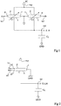
- the figure 1 schematically illustrates a logic cell of the type described in the aforementioned patent applications.
- the cell of the figure 1 includes two variable capacitance capacitors C1 and C2.
- Each of the capacitors C1 and C2 is a device with four electrodes d, s, g and r electrically isolated from each other.
- the electrodes d and s called the main electrodes, are movable relative to each other.
- the electrodes g and r, called control electrodes are intended to receive a control signal, for example a voltage or a current, adapted to vary the relative position of the electrodes d and s so as to vary the value of the capacitance Cds between electrodes d and s.
- the main electrodes d of capacitors C1 and C2 are connected to the same node sup application of a PC supply voltage to the cell.
- the main electrodes s of capacitors C1 and C2 are connected to the same node out for supplying an output signal S of the cell.
- the control electrode g of the capacitor C1 is connected to a node in1 for applying an input logic signal A of the cell, and the control electrode g of the capacitor C2 is connected to a node in2 for applying an input logic signal B of the cell.
- the control electrodes r of capacitors C1 and C2 are connected to the same node GND for applying a reference potential of the cell, for example ground.
- the capacitors C1 and C2 are capacitors with a positive variation in capacitance, that is to say that the capacitance of each capacitor between its main electrodes d and s takes a high value when the signal applied between its control electrodes g and r is at a high value, and takes a low value when the signal applied between its control electrodes g and r is at a low value.
- European patent applications No. 16204534 and American N ° 15/381477 mentioned above describe examples of cells suitable for implementing various basic logic functions with two binary inputs and one binary output, and in particular the logic functions AND, NOT AND and NOT OR, from two capacitors with variable capacitance with four electrodes.
- one embodiment provides a capacitive logic cell as disclosed in independent claim 1.
- the first and second logic input signals are referenced with respect to said application node of a first reference potential.
- the cell further comprises a sixth electrode electrically isolated from the first, second, third, fourth and fifth electrodes, the sixth electrode being connected to a node of application of the second reference potential, the first logic signal d 'input being referenced with respect to the application node of a first reference potential and the second logic input signal being referenced with respect to the application node of the second reference potential.
- the movable assembly is movable in translation relative to the fixed assembly so as to vary the area of the second electrode facing the first electrode without varying the distance between the first and second electrodes.
- the mobile assembly is movable in translation relative to the fixed assembly so as to vary the distance between the first and second electrodes. without varying the surface of the second electrode vis-à-vis the first electrode.
- the cell comprises a first electrostatic actuation device capable of causing a displacement of the movable assembly relative to the fixed assembly as a function of the state of the first logic input signal, and a second electrostatic actuation device capable of causing a displacement of the movable assembly relative to the fixed assembly as a function of the state of the second logic input signal.
- the cell comprises an electrostatic actuation device capable of causing a displacement of the movable assembly relative to the fixed assembly as a function of the state of the first logic input signal, and a device for electrodynamic actuation capable of causing a displacement of the movable assembly relative to the fixed assembly as a function of the state of the second logic input signal.
- the first electrode comprises first and second interconnected conductive portions, arranged on either side of the second electrode so as to limit the influence of the voltage between the first and second electrodes on the position of the electrode. 'mobile assembly relative to the fixed assembly.
- the cell comprises a seventh electrode connected to a node for applying a third logic input signal of the cell, the position of the second electrode relative to the first electrode being a function of a combination first, second and third input logic signals.
- the fixed assembly comprises an eighth electrode electrically isolated from the first electrode, the eighth and second electrodes defining a second variable capacitance as a function of the position of the movable assembly with respect to the fixed assembly.
- the eighth electrode is connected to a node for supplying a second logic output signal of the cell.
- connection is used to denote a direct electrical connection, without an intermediate electronic component, for example by means of one or more conductive tracks, and the term “coupled” or the term “connected”, for designate a link which can be direct (meaning then "connected") or which can be carried out by means of one or more components.
- orientation qualifiers such as the terms “horizontal”, “vertical”, etc., reference is made to the orientation of the figures, it being understood that, in In practice, the devices described can be oriented differently.
- plate is meant conductive a plate made of a material capable of conducting electric charges, this material possibly being a conductive material, for example a metal, or else a semiconducting material, for example silicon.
- capacitive logic cells described in European patent application No. 16204534 and in U.S. Patent Application No. 15/381477 mentioned above (the content of which is incorporated here by reference to the extent permitted by law) encode logic states mechanically (via a relative position between the main electrodes of each capacitor). This mechanical coding makes it possible to dispense with the usual compromise in energy, between dissipation by conduction and dissipation by leakage, inherent in all logic cells based on transistors. On the other hand, electromechanical transduction creates losses at each change of logic state.
- a logic cell is provided based on a single variable capacitance capacitor with five electrodes. , instead of two variable capacitance capacitors with four electrodes in the aforementioned European and American patent applications.
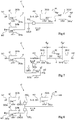
- the figure 2 is an electrical diagram of an example of an embodiment of a capacitive logic cell.
- the cell of the figure 2 comprises a capacitor with variable capacity C.
- the capacitor C is a device with five electrodes d, s, g1, g2 and r electrically isolated from each other.
- the electrodes d and s called the main electrodes, are movable relative to each other.
- the electrodes g1, g2 and r, called control electrodes are intended to receive control signals, for example voltages or currents, adapted to vary the relative position of the electrodes d and s so as to vary the value of the capacitance Cds between the electrodes d and s.
- a first control signal can be applied between the electrodes g1 and r and a second control signal can be applied between the electrodes g2 and r, the relative position of the electrodes d and s, and therefore the capacitance Cds of capacitor C, being a function of a combination of the first and second control signals.
- the main electrode d of capacitor C is connected to a node sup for applying a supply voltage PC to the cell, for example a direct voltage (in the case of an implementation of a static logic circuit in which the states of the logic signals are available at all times), or, preferably, a periodic variable voltage (in the case of an implementation of a dynamic logic circuit in which the states of the logic signals are available only during a part of the period of a periodic clock signal as described in European patent applications No. 16204534 and American N ° 15/381477 mentioned above), for example a trapezoidal tension.
- the main electrode s of capacitor C is connected to an out node for supplying an output logic signal S of the cell.
- the control electrode g1 of the capacitor C is connected to a node in1 of application of an input logic signal A of the cell, and the control electrode g2 of the capacitor C is connected to a node in2 of application an input logic signal B of the cell.
- the control electrode r of capacitor C is connected to a node GND for applying a reference potential of the cell, for example ground.
- a capacitor C L connected between the output node out and the reference node GND has also been shown, schematically showing the output capacitance of the cell.
- the output capacitor C L may not include a component specifically produced and connected to the output node out, but correspond to the sum of the capacitances of the various elements connected to the node out, in particular the interconnection tracks, or yet another capacitive logic cell (not shown) whose input can be connected to the out node.
- the input signals A and B, the output signal S and the power supply signal PC of the cell are referenced with respect to the node GND.
- the cell of the figure 2 behaves like a capacitive voltage divider bridge comprising a controllable capacitor corresponding to the capacitance Cds of the capacitor C, and a fixed capacitance formed by the capacitance C L of the output node out of the cell.
- variable-capacity capacitor C The logic function performed by the cell depends on the arrangement of the variable-capacity capacitor C.
- Various embodiments of the variable-capacity capacitor C, suitable for the implementation of various basic logic functions, will now be described.
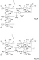
- the figure 3 is a simplified sectional view of an exemplary embodiment of the variable capacitance capacitor C of the cell of the figure 2 , suitable for the implementation of an OR logic operation.
- the capacitor C comprises two assemblies movable with respect to one another, called hereinafter respectively fixed assembly and movable assembly. All the elements of the fixed assembly are fixed with respect to each other, and all the elements of the movable assembly are fixed with respect to each other. On the figure 3 as well as in the following figures, there is represented by oblique hatching a mechanical mass, to which all the elements of the fixed assembly are fixed.
- the electrodes s, g1 and g2 are part of the fixed assembly, and the electrodes d and r are part of the moving assembly.
- the square referenced 320 on the figure 3 shows schematically an electrically insulating region separating the electrodes d and r of the mobile assembly.
- the electrode s comprises two conductive plates 301a and 301b substantially horizontal and facing each other (that is to say substantially coincident in vertical projection), electrically connected to the output node out of the cell.
- the electrode g1 comprises two conductive plates 303a and 303b which are substantially horizontal and facing each other, electrically connected to the input node in1 of the cell.
- the electrode g2 comprises two conductive plates 305a and 305b which are substantially horizontal and facing each other, electrically connected to the input node in2 of the cell.
- Electrode d comprises a substantially horizontal conductive plate 302 electrically connected to the upper power supply node of the cell.
- the electrode r comprises two conductive plates 304 and 306 that are substantially horizontal, electrically connected to the reference node GND of the cell.
- the mobile assembly is free to move according to a single degree of freedom in horizontal translation (parallel to the conductive plates 301a, 301b, 302, 303a, 303b, 304, 305a, 305b, 306) relative to the fixed assembly, so as to modify the surface of the movable conductive plate 302, respectively 304, respectively 306 facing the corresponding fixed conductive plates 301a and 301b, respectively 303a and 303b, respectively 305a and 305b, without modifying the distance between each movable conductive plate and the corresponding fixed conductive plates (movement represented by a double arrow MV in the figure).
- the fixed assembly and the movable assembly are arranged so that when the surface of any one of the movable conductor plates 302, 304 and 306 facing the corresponding fixed conductor plates 301a and 301b, respectively 303a and 303b, 305a and 305b respectively increases, the area of the other movable conductive plates facing the corresponding fixed conductive plates increases, and vice versa.
- the capacitor C of the figure 3 further comprises return means (not visible in the figure), for example a return spring, arranged for, in the absence of any electrical polarization of the electrodes g1, g2, s and d with respect to the electrode r, return the movable assembly to a so-called rest position (relative to the fixed assembly), in which the movable conductive plates 302, 304 and 306 are only partially opposite the corresponding fixed conductive plates 301a and 301b , respectively 303a and 303b, respectively 305a and 305b (for example the position shown on the figure 3 ).
- return means not visible in the figure
- a return spring arranged for, in the absence of any electrical polarization of the electrodes g1, g2, s and d with respect to the electrode r, return the movable assembly to a so-called rest position (relative to the fixed assembly), in which the movable conductive plates 302, 304 and 306 are only partially opposite the corresponding fixed conductive plates 301a and
- the capacitance Cds of the capacitor C between its main electrodes s and d is proportional to the area of the conductive plate 302 vis-à-vis the conductive plates 301a and 301b.
- the input A and B and output S logic signals are voltages.
- the capacitor C When the input signals A and B are in a low state, that is to say at a voltage level lower (in absolute value) than a threshold Vin L , for example at a substantially zero voltage, the capacitor C is in its rest position, and the capacitance Cds of capacitor C has a first value.
- the output signal S of the cell therefore has a first voltage level Vout1.
- the electrostatic force exerted by the conductive plates 303a and 303b on the conductive plate 304 and the electrostatic force exerted by the conductive plates 305a and 305b on the conductive plate 306 are added.
- the horizontal displacement of the mobile assembly relative to the fixed assembly is therefore amplified.
- the capacitor Cds of the capacitor C then takes a third value greater than the second value, and the output signal S of the cell has a third voltage level Vout3 greater (in absolute value) than the second level.
- capacitor C is sized so that the high logic state of the output signal S is interpreted as a high logic state when it is applied to the input in1 or in2 of the cell, and so that l The low logic state of the output signal S is interpreted as a low logic state when it is applied to the input in1 or in2 of the cell.
- the capacitor C of the figure 3 is dimensioned so that the output voltage levels Vout2 and Vout3 are greater than the threshold Vin H , and so that the output voltage level Vout1 is less than the threshold Vin L.
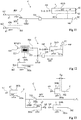
- the figure 4 is a simplified sectional view of another embodiment of the variable capacitance capacitor C of the cell of the figure 2 , suitable for the implementation of an AND logic operation.
- the capacitor C of the figure 4 differs from capacitor C of the figure 3 mainly in that, in the example of figure 4 , in the rest position of the capacitor, the conductive plates 302 on the one hand, and 301a and 301b on the other hand, do not overlap. In other words, in the rest position, the conductive plate 302 is not opposite the conductive plates 301a and 301b. More particularly, in the rest position, in vertical projection, a non-overlapping distance d ar separates the conductive plate 302 from the conductive plates 301a and 301b.
- the capacitor C of the figure 4 is the same or similar to the capacitor C of the figure 3 .
- the capacitance Cds of the capacitor is zero or negligible.
- the output signal S of the cell therefore has a zero or negligible voltage level, corresponding to a low logic state of the signal S.
- the corresponding movable conductor plate 304 or 306 When only one of the input signals A and B is high, the corresponding movable conductor plate 304 or 306 is attracted between the corresponding fixed conductor plates 303a and 303b or 305a and 305b, by electrostatic interaction. This causes a horizontal displacement of the movable assembly relative to the fixed assembly, tending to reduce the non-overlap distance d ar between the conductive plate 302 and the conductive plates 301a and 301b, without however canceling it. Thus, the capacitance Cds of the capacitor remains zero or negligible, and the output signal S of the cell remains in the low state.
- the horizontal displacement of the movable assembly relative to the fixed assembly is amplified, and the conductive plate 302 enters between the conductive plates 301a and 301b .
- the capacitance Cds of the capacitor C then takes a non-negligible value, and the output signal S of the cell takes on a non-negligible voltage level, corresponding to a high logic state of the signal S.
- the figure 5 is a simplified sectional view of another embodiment of the variable capacitance capacitor C of the cell of the figure 2 , suitable for the implementation of an AND logic operation.
- the capacitor C of the figure 5 differs from capacitor C of the figure 3 mainly in that, in the example of figure 5 , in the rest position of the capacitor, the conductive plates 306 on the one hand, and 305a and 305b on the other hand, do not not cover. In other words, in the rest position, the conductive plate 306 is not opposite the conductive plates 305a and 305b. More particularly, in the rest position, in vertical projection, a non-overlap distance d ar separates the conductive plate 306 from the conductive plates 305a and 305b.
- the capacitor C of the figure 5 is the same or similar to the capacitor C of the figure 3 .
- the capacitor C When the signal A is in the low state, the capacitor C remains in its rest position regardless of the state of the signal B. In particular, even if the signal B is in the high state, the electrostatic force exerted on the conductive plate 306 by conductive plates 305a and 305b is negligible due to the non-overlap of electrodes 306 and 305a, 305b.
- the capacitor Cds of the capacitor C then has a first value, and the output signal S of the cell a first voltage level corresponding to a low logic state of the signal S.
- the electrostatic force exerted on the movable conductive plate 304 by the fixed conductive plates 303a and 303b causes a horizontal displacement of the movable assembly relative to the fixed assembly, tending to increase the surface of the conductive plate 304 facing the conductive plates 303a and 303b.
- the capacitance Cds of the capacitor C then has a second value greater than the first value, and the output signal S of the cell has a second voltage level greater (in absolute value) than first level, still corresponding to the low logic state of signal S. If, on the other hand, signal B is in the high state, the electrostatic force exerted on the conductive plate 306 by the conductive plates 305a and 305b tends to amplify the horizontal displacement of the mobile assembly with respect to the fixed assembly, leading to increasing the area of the conductive plate 302 vis-à-vis the conductive plates 301a and 301b. The capacitance Cds of the capacitor C then has a third value greater than the second value, and the output signal S of the cell has a third voltage level greater (in absolute value) than the second level, corresponding to the high logic state of the cell. signal S.
- the figure 6 is a simplified sectional view of another embodiment of the variable capacitance capacitor C of the cell of the figure 2 , suitable for the implementation of an OR logic operation.
- the capacitor C of the figure 6 comprises the same elements as the capacitor C of the figure 5 , arranged substantially in the same way.
- the electrode d of the capacitor comprises an additional substantially horizontal conductive plate 302 ', fixed with respect to the conductive plate 302, and electrically connected to the conductive plate 302.
- the electrode s of the capacitor comprises two additional conductive plates 301a 'and 301b' substantially horizontal and facing each other, fixed relative to the conductive plates 301a and 301b, and electrically connected to the conductive plates 301a and 301b.
- the fixed assembly and the movable assembly are arranged so that the conductive plate 302 'is disposed between the conductive plates 301a' and 301b ', at least partially facing the conductive plates 301a' and 301b ', substantially equidistant from the conductive plates 301a 'and 301b'.
- the fixed assembly and the movable assembly are arranged so that when the area of the conductive plate 302 facing the conductive plates 301a and 301b increases, the area of the conductive plate 302 'opposite screw of the conductive plates 301a 'and 301b' decreases, and vice versa.
- the lateral displacement should be sufficient so that the plate 302 'is no longer facing the plates. 301a ', 301b', so that the decrease in the capacity between the plates 302 'and 301a', 301b 'is no longer compensated for by the increase in the capacity between the plates 302 and 301a, 301b.
- the displacement linked to the application of the input signals A and B should be greater than the initial overlap between the plates 302 'and 301a', 301b '.
- the figure 7 is a simplified sectional view of another embodiment of the variable capacitance capacitor C of the cell of the figure 2 , suitable for the implementation of an EXCLUSIVE OR logic operation.
- the capacitor C of the figure 7 includes elements common with the capacitor C of the figure 6 . Only the differences between the two capacitors will be detailed below.
- the capacitor C of the figure 7 differs from capacitor C of the figure 6 in that, in the example of figure 7 , in the rest position of the capacitor, the conductive plates 302 on the one hand, and 301a and 301b on the other hand, do not overlap. In addition, in the rest position of the capacitor, the conductive plates 302 'on the one hand, and 301a' and 301b 'on the other hand, do not overlap.
- a non-overlap distance d ar separates the conductive plate 302 from the conductive plates 301a and 301b
- a non-overlap distance ar ' for example substantially identical, separates the plate conductor 302 'of the conductive plates 301a' and 301b '.
- the capacitor C When the input signals A and B are at a low state, the capacitor C is in its rest position. Due to the non-overlap between the conductive plate 302 and the conductive plates 301a, 301b on the one hand, and between the conductive plate 302 'and the conductive plates 301a' and 301b 'on the other hand, the capacitance Cds of the capacitor C is nil or negligible. The output signal S of the cell therefore has a zero or negligible voltage level, corresponding to a low logic state of the signal S.
- the electrostatic force exerted by the conductive plates 303a and 303b on the conductive plate 304 compensates for the electrostatic force exerted by the conductive plates 305a and 305b on the conductive plate 306, therefore. so that the capacitor C remains in its rest position.
- the output signal S of the cell therefore remains in the low state of the signal S.
- the electrostatic force exerted by the conductive plates 303a and 303b on the conductive plate 304 causes a horizontal displacement of the movable assembly with respect to the 'fixed assembly, tending to increase the surface of the conductive plate 304 vis-à-vis the conductive plates 303a and 303b.
- the conductive plate 302 penetrates between the conductive plates 301a and 301b.
- the capacitance Cds of the capacitor C then takes a non-negligible value, and the output signal S of the cell takes on a non-negligible voltage level, corresponding to a high logic state of the signal S.
- the electrostatic force exerted by the conductive plates 305a and 305b on the conductive plate 306 causes a horizontal displacement of the movable assembly. relative to the fixed assembly, tending to increase the area of the conductive plate 306 vis-à-vis the conductive plates 305a and 305b.
- the conductive plate 302 'penetrates between the conductive plates 301a' and 301b '.
- the capacitance Cds of the capacitor C then takes a non-negligible value, and the output signal S of the cell takes on a non-negligible voltage level, corresponding to a high logic state of the signal S.
- the figure 8 is a simplified sectional view of another embodiment of a variable capacitance capacitor C suitable for implementing an OR logic operation.
- the capacitor of the figure 8 differs from the previous examples in that it comprises six electrodes electrically isolated from each other, instead of five in the previous examples. More particularly, in the capacitor of the figure 8 , the electrode r is replaced by two electrodes r1 and r2 electrically insulated from one another, each of the electrodes r1 and r2 being electrically insulated from the electrodes d, s, g1 and g2.
- the electrodes of capacitor C of the figure 8 are for example connected in a similar or identical manner to what has been described above, with the difference that the electrode r1 and the electrode r2 are connected to nodes GND1 and GDN2 for applying distinct reference potentials.
- a first control signal can be applied between the electrodes g1 and r1 and a second control signal can be applied between the electrodes g2 and r2, the relative position of the electrodes d and s, and therefore the capacitance Cds of the capacitor C, being a function of a combination of the first and second control signals.
- the electrodes r1 and r2 are part of the moving assembly of the capacitor C.
- the square referenced 320 1 schematically shows an electrically insulating region separating the electrode r1 from the electrodes d and r2 of the mobile assembly
- the square referenced 320 2 schematically represents an electrically insulating region separating the electrode r2 from the electrodes d and r1.
- the capacitor C of the figure 8 comprises the same elements as the capacitor C of the figure 3 , arranged substantially in the same way, and differs from the capacitor C of the figure 3 essentially in that, in the example of figure 8 , the conductive plates 304 and 306 are electrically isolated from each other.
- the conductive plate 304 is connected to the node GND1 and forms the electrode r1 of the capacitor
- the conductive plate 306 is connected to the node GND2 and forms the electrode r2 of the capacitor.
- An advantage of the capacitor C of the figure 8 is that it makes it possible to perform a logical operation relating to signals referenced with respect to distinct potentials.
- the figure 9 is a simplified sectional view of another embodiment of a variable capacitance capacitor C suitable for implementing an OR logic operation. Unlike the examples described above in which the capacitor C makes it possible to perform logic operations with two inputs and one output, the capacitor C of the figure 9 enables a logic operation with three inputs and one output.
- the capacitor C of the figure 9 comprises the same elements as the capacitor C of the figure 3 , arranged substantially in the same way.
- the capacitor C of the figure 9 further comprises an additional control electrode g3, electrically isolated from the electrodes d, s, g1, g2 and r.
- the electrode g3 is part of the fixed assembly of the capacitor.
- the electrode g3 comprises two conductive plates 307a and 307b substantially horizontal and facing one another, electrically connected to a third input node in3 of the cell.
- the electrode r comprises an additional substantially horizontal conductive plate 308, electrically connected to the reference node GND of the cell.
- the fixed assembly and the movable assembly are arranged so that the conductive plate 308 is disposed between the conductive plates 307a and 307b, at least partially facing the conductive plates 307a and 307b, substantially equidistant from the conductive plates 307a and 307b. More particularly, in the example of figure 9 , the fixed assembly and the movable assembly are arranged so that when the area of the conductive plate 308 facing the conductive plates 307a and 307b increases, the area of the conductive plate 302 opposite conductive plates 301a and 301b increases, and vice versa.
- the nodes in1, in2 and in3 of the capacitor C are intended to receive respectively input logic signals A1, A2 and A3.
- the capacitor C When the input signals A1, A2 and A3 are low, the capacitor C is in its rest position, and the capacitor Cds of the capacitor C has a first value.
- the output signal S of the cell therefore has a first voltage level Vout1.
- the horizontal displacement of the mobile assembly with respect to the fixed assembly is amplified, and the capacitance Cds of the capacitor C takes a third value greater than the second value.
- the output signal S of the cell then takes a third voltage level Vout3 greater (in absolute value) than the second level.
- the horizontal displacement of the movable assembly relative to the fixed assembly is further amplified, and the capacitance Cds of the capacitor C takes a fourth value greater than the third value.
- the output signal S of the cell then takes a fourth voltage level Vout4 higher (in absolute value) than the third level.
- the figure 10 is a simplified sectional view of another embodiment of a variable capacitance capacitor C suitable for implementing an OR logic operation. Unlike the examples described above in which the capacitor C makes it possible to perform logic operations with N inputs and one output, the capacitor C of the figure 9 enables a logic operation with N inputs and two outputs.
- the capacitor C of the figure 10 comprises the same elements as the capacitor C of the figure 3 , arranged substantially in the same way.
- the capacitor C of the figure 10 further comprises an additional main electrode s', electrically isolated from the electrodes s, d, g1, g2 and r.
- the electrode is part of the fixed assembly of the capacitor.
- the electrode s ' comprises two additional conductive plates 309a and 309b substantially horizontal and vis-à-vis one another, electrically connected to a second output node out' of the cell.
- the electrode d comprises an additional substantially horizontal conductive plate 310, electrically connected to the upper supply node of the cell.
- the fixed assembly and the movable assembly are arranged so that the conductive plate 310 is disposed between the conductive plates 309a and 309b, at least partially facing the conductive plates 309a and 309b, substantially equidistant from the conductive plates 309a and 309b. More particularly, in the example of figure 10 , the fixed assembly and the movable assembly are arranged so that when the surface of the conductive plate 302 facing the conductive plates 301a and 301b increases, the surface of the conductive plate 310 opposite the conductive plates 309a and 309b increases, and vice versa.
- the out and out 'nodes are intended to respectively supply logic output signals S and S'.
- the capacitance Cds 'of the capacitor between the electrodes d and s' evolves substantially in the same way as the capacitance Cds of the capacitor between the electrodes d and s.
- the logic output signal S ′ supplied on the output node out ′ is an image of the logic output signal S supplied on the output node out.
- An advantage of this configuration is that it makes it possible to provide the result of the logical combination of signals A and B on two separate output nodes electrically isolated from one another.
- the figure 11 is a simplified sectional view of another embodiment of the variable capacitance capacitor C of the cell of the figure 2 , suitable for the implementation of an OR logic operation.
- the capacitor C of the figure 11 includes elements common with the capacitor C of the figure 3 . Only the differences between the two capacitors will be detailed below.
- the electrode s of the capacitor comprises two conductive plates 401a and 401b which are substantially horizontal and opposite each other, electrically connected to the output node out of the cell.
- the electrode g1 of the capacitor comprises a substantially horizontal conductive plate 403, electrically connected to the input node in1 of the cell.
- the electrode g2 of the capacitor comprises a substantially horizontal conductive plate 405, electrically connected to the input node in2 of the cell.
- the electrode d of the capacitor includes a conductive plate 402 substantially horizontal, electrically connected to the upper power supply node of the cell.
- the electrode r of the cell comprises two substantially horizontal conductive plates 404 and 406, electrically connected to the reference node GND of the cell.
- the mobile assembly is free to move according to a single degree of freedom in vertical translation (orthogonally to the conductive plates 401a, 401b, 402, 403, 404, 405, 406) relative to the fixed assembly (movement represented by a double arrow MV in the figure), so as to modify the distance between the movable conductor plate 402 and the fixed conductor plates 401a and 401b, the distance between the movable conductor plate 404 and the fixed conductor plate 403, and the distance between the movable conductive plate 406 and the fixed conductive plate 405, without modifying the surface of the movable conductive plate 402 facing the fixed conductive plates 401a and 401b, the surface of the movable conductive plate 404 facing one another screw of the fixed conductor plate 403, and the surface of the movable conductor plate 406 facing the fixed conductor plate 405.
- the fixed assembly and the movable assembly are arranged so that when the distance between any one of the movable conductive plates 402, 404 and 406 and the corresponding fixed conductive plate 401a, respectively 403, respectively 405 increases, the distance between the other movable conductor plates and the fixed conductor plates increase by the same value, and vice versa.
- the distance between the conductive plate 402 and the conductive plate 401a increases, the distance between the conductive plate 402 and the conductive plate 401b decreases, and vice versa.
- the capacitor C can also include return means (not visible in the figure), for example a return spring, arranged for, in the absence of any electrical polarization of the electrodes g1, g2, s and d with respect to l 'electrode r, bring the movable assembly back to a so-called rest position, for example a position in which the movable conductor plate 402 is located equidistant from the fixed conductor plates 401a and 401b (corresponding to the position shown on the figure figure 11 ).
- return means not visible in the figure
- a return spring arranged for, in the absence of any electrical polarization of the electrodes g1, g2, s and d with respect to l 'electrode r, bring the movable assembly back to a so-called rest position, for example a position in which the movable conductor plate 402 is located equidistant from the fixed conductor plates 401a and 401b (corresponding to the position shown on the figure figure 11 ).
- the capacitance Cds of the capacitor C between its main electrodes s and d is equal to the sum of a capacitance Cds1 formed between the conductive plate 401a and the conductive plate 402, and of a capacitance Cds2 formed between the conductive plate 401b and the conductive plate 402, the capacitors Cds1 and Cds2 being respectively inversely proportional to the distance d1 between the plates 401a and 402 and inversely proportional to the distance d2 between the plates 401b and 402.
- the capacitance Cds takes a minimum value when the conductive plate 402 is equidistant from the conductive plates 401a and 401b.
- the capacitor C When the control signals A and B are in the low state, the capacitor C is in its rest position, and the capacitance Cds of the capacitor C has a first value, corresponding here to its minimum value.
- the output signal S of the cell therefore has a first relatively low voltage level Vout1.
- This causes a vertical displacement of the movable assembly relative to the fixed assembly, tending to reduce the distance d1 between the movable conductive plate 402 and the fixed conductive plate 401a.
- the movable conductive plate 402 comes to rest against the conductive plate 401a, at a distance from the conductive plate 401a fixed by the stop or stops of the capacitor.
- the capacitance Cds of the capacitor C thus takes on a second value greater than the first value.
- the output signal S of the cell then has a second voltage level Vout2 greater (in absolute value) than the first level.
- the vertical displacement of the movable assembly relative to the fixed assembly is similar, i.e. the movable conductive plate 402 comes to rest. press against the conductive plate 401a, at a distance from the conductive plate 401a fixed by the stopper (s) of the capacitor.
- the capacitor Cds of the capacitor C then takes the second value, and the output signal S of the cell is at the second voltage level Vout2.
- the electrode s comprises two conductive plates 401a and 401b arranged on either side of the conductive plate 402 forming the electrode d. This advantageously makes it possible to reduce the influence of the voltage Uds between the electrodes s and d on the value of the capacitor Cds, or even to cancel the influence of the voltage Uds on the value of the capacitor Cds when the conductive plate 402 is equidistant from the conductive plates 401a and 401b.
- one of the conductive plates 401a and 401b can be omitted. It will be noted that in this example, if the conductive plate 401b is omitted and the conductive plate 401a preserved, the logic function performed is an OR function, and, if the conductive plate 401a is omitted and the conductive plate 401b retained, the logic function performed is a NOT OR function.
- the figure 12 is a simplified sectional view of another embodiment of the variable capacitance capacitor C of the cell of the figure 2 , suitable for the implementation of an OR logic operation.
- the capacitor C of the figure 12 includes elements common with the capacitor C of the figure 3 . In the following, only the differences between the two structures will be detailed.
- the capacitor C of the figure 12 differs from capacitor C of the figure 3 mainly in that it implements an actuation of the electromagnetic type, also called electrodynamics, combined with an actuation of the type electrostatic, instead of purely electrostatic actuation as in the example of figure 3 .
- terminals 503 and 504 and coil 521 are part of the fixed capacitor assembly, and magnet 523 is part of the movable capacitor assembly.
- the terminals 503 and 504 and the coil 521 are fixed with respect to the conductive plates 301a, 301b, 305a and 305b, and the magnet 523 is fixed with respect to the conductive plates 306 and 302.
- the axis center of coil 521 is substantially horizontal.
- the structure of the figure 12 has the advantage of making it possible to perform a logic operation having for operands electrical signals of different kinds, namely a logic signal A in current and a logic signal B in voltage in the example shown.
- the structure can be modified to replace the electrostatic actuation mechanism. associated with the electrode g2 by an electrodynamic actuation mechanism, so as to produce a purely electrodynamic actuation capacitor.
- the figure 13 is a simplified sectional view of another embodiment of a variable capacitance capacitor C, suitable for the successive implementation of two distinct logic operations with an input and an output, a YES operation (buffer) and an operation NO (changeover), for two separate inputs.
- the capacitor C of the figure 13 includes elements common with the capacitor C of the figure 4 . Only the differences between the two structures will be detailed below.
- the fixed assembly in addition to the conductive plates 301a, 301b, 303a, 303b, 305a, 305b, the fixed assembly comprises two additional conductive plates 501a and 501b substantially horizontal and facing each other, electrically connected to the node output out of the cell.
- the electrode s of the capacitor is formed by the conductive plates 301a, 301b, 501a and 501b.
- the movable assembly of the capacitor C of the figure 13 comprises an additional substantially horizontal conductive plate 502, electrically connected to the upper power supply node of the cell.
- the electrode d of the capacitor is formed by the plates 302 and 502.
- the fixed assembly and the movable assembly are arranged so that the additional movable conductive plate 502 is disposed between the conductive plates 501a and 501b, at least partially facing the conductive plates 501a and 501b, substantially equidistant from the conductive plates 501a and 501b.
- the signal B when the YES function is used, the signal B must be set low or the node in2 must be left floating, and, when the function NOT is used, the signal A must be set low, or node in1 must be left floating.
- An advantage of the embodiment of the figure 13 is that it makes it possible, by means of the same logic cell with two inputs and one output, to implement two distinct logic functions, selectable by the choice of the input to which the input logic signal is applied.
- the figure 14 is a simplified sectional view of another embodiment of the variable capacitance capacitor C of the figure 2 , suitable for the implementation of a NOR logic function.
- the capacitor C of the figure 14 differs from capacitor C of the figure 3 essentially in that, in the example of figure 14 , the fixed assembly and the movable assembly are arranged so that when the area of one of the movable conductive plates 304 and 306 facing the corresponding fixed conductive plates 303a and 303b, respectively 305a and 305b, increases, the surface of the movable conductive plate 302 opposite the corresponding fixed conductive plates 301a and 301b decreases, and vice versa.
Landscapes
- Engineering & Computer Science (AREA)
- Physics & Mathematics (AREA)
- Computer Hardware Design (AREA)
- Computing Systems (AREA)
- General Engineering & Computer Science (AREA)
- Mathematical Physics (AREA)
- Power Engineering (AREA)
- Microelectronics & Electronic Packaging (AREA)
- Semiconductor Integrated Circuits (AREA)
- Charge And Discharge Circuits For Batteries Or The Like (AREA)
- Condensed Matter Physics & Semiconductors (AREA)
- General Physics & Mathematics (AREA)
- Micromachines (AREA)
Claims (9)
- Kapazitive Logikzelle, die einen Kondensator (C) mit variabler Kapazität aufweist, der eine erste (s), zweite (d), dritte (g1), vierte (g2) und fünfte (r; r1) Elektrode aufweist, die elektrisch voneinander isoliert sind, wobei der Kondensator (C) eine feste Baugruppe, die die erste Elektrode (s) aufweist, und eine bewegliche Baugruppe, die die zweite Elektrode (d) aufweist, aufweist, wobei:die erste (s) und die zweite (d) Elektrode eine erste variable Kapazität des Kondensators (C) in Abhängigkeit von der Position der beweglichen Baugruppe relativ zu der festen Baugruppe definieren;die dritte Elektrode (g1) mit einem Knoten (in1) zum Anlegen eines ersten logischen Eingangssignals (A; A1) der Zelle verbunden ist;die vierte Elektrode (g2) mit einem Knoten (in2) zum Anlegen eines zweiten logischen Eingangssignals (B; A2) der Zelle verbunden ist;die fünfte Elektrode (r; r1) mit einem Knoten (GND; GND1) zum Anlegen eines ersten Bezugspotentials der Zelle verbunden ist; unddie Position der zweiten Elektrode (d) relativ zur ersten Elektrode (s) eine Funktion einer Kombination des ersten (A; A1) und zweiten (B; A2) logischen Eingangssignals ist,wobei:die bewegliche Baugruppe in Bezug auf die feste Baugruppe translatorisch beweglich ist, um den Oberflächenbereich der zweiten Elektrode (d) gegenüber der ersten Elektrode (s) zu verändern, ohne den Abstand zwischen der ersten (s) und der zweiten (d) Elektrode zu verändern; oderdie bewegliche Baugruppe in Bezug auf die feste Baugruppe translatorisch beweglich ist, um den Abstand zwischen der ersten (s) und der zweiten (d) Elektrode zu variieren, ohne den Oberflächenbereich der zweiten Elektrode (d) gegenüber der ersten Elektrode (s) zu verändern,und wobei:die zweite Elektrode (d) mit einem Knoten (sup) zum Anlegen einer Stromversorgungsspannung (PC) der Zelle verbunden ist;die erste Elektrode (s) mit einem Knoten (out) zum Liefern eines ersten logischen Ausgangssignals (S) der Zelle verbunden ist; undeine Ausgangskapazität (CI) zwischen der ersten Elektrode (s) und dem Knoten (GND; GND1) zum Anlegen des ersten Bezugspotentials der Zelle angeschlossen ist.
- Zelle nach Anspruch 1, wobei das erste (A) und das zweite (B) logische Eingangssignal auf den Knoten (GND) zum Anlegen eines ersten Bezugspotentials bezogen sind.
- Zelle nach Anspruch 1, die weiterhin eine sechste (r2) Elektrode aufweist, die von der ersten (s), zweiten (d), dritten (g1), vierten (g2) und fünften (r1) Elektrode elektrisch isoliert ist, wobei die sechste Elektrode (r2) mit einem Knoten (GND2) zum Anlegen eines zweiten Bezugspotentials verbunden ist, wobei das erste logische Eingangssignal (A) auf den Knoten (GND1) zum Anlegen eines ersten Bezugspotentials bezogen ist und das zweite logische Eingangssignal (B) auf den Knoten (GND2) zum Anlegen eines zweiten Bezugspotentials bezogen ist.
- Zelle nach einem der Ansprüche 1 bis 3, mit einer ersten elektrostatischen Betätigungsvorrichtung, die in der Lage ist, eine Verschiebung der beweglichen Baugruppe in Bezug auf die feste Baugruppe in Abhängigkeit vom Zustand des ersten logischen Eingangssignals (A) zu bewirken, und mit einer zweiten elektrostatischen Betätigungsvorrichtung, die in der Lage ist, eine Verschiebung der beweglichen Baugruppe in Bezug auf die feste Baugruppe in Abhängigkeit vom Zustand des zweiten logischen Eingangssignals (B) zu bewirken.
- Zelle nach einem der Ansprüche 1 bis 3, mit einer elektrostatischen Betätigungsvorrichtung, die in der Lage ist, eine Verschiebung der beweglichen Baugruppe in Bezug auf die feste Baugruppe in Abhängigkeit vom Zustand des ersten logischen Eingangssignals (A) zu bewirken, und mit einer elektrodynamischen Betätigungsvorrichtung, die in der Lage ist, eine Verschiebung der beweglichen Baugruppe in Bezug auf die feste Baugruppe in Abhängigkeit vom Zustand des zweiten logischen Eingangssignals (B) zu bewirken.
- Zelle nach einem der Ansprüche 1 bis 5, wobei die erste Elektrode (s) erste (301a, 301b; 401a) und zweite (301a', 301b'; 401b) miteinander verbundene leitende Abschnitte aufweist, die auf beiden Seiten der zweiten Elektrode (d) angeordnet sind, um den Einfluss der Spannung zwischen der ersten (s) und der zweiten (d) Elektrode auf die Position der beweglichen Baugruppe relativ zur festen Baugruppe zu begrenzen.
- Zelle nach einem der Ansprüche 1 bis 6, die eine siebte Elektrode (g3) aufweist, die mit einem Knoten (in3) zum Anlegen eines dritten logischen Eingangssignals (A3) der Zelle verbunden ist, wobei die Position der zweiten Elektrode (d) relativ zur ersten Elektrode (s) eine Funktion einer Kombination des ersten (A1), zweiten (A2) und dritten (A3) logischen Eingangssignals ist.
- Zelle nach einem der Ansprüche 1 bis 7, wobei die feste Baugruppe eine achte Elektrode (s') aufweist, die von der ersten Elektrode (s) elektrisch isoliert ist, wobei die achte (s') und zweite (d) Elektrode einen zweiten Kondensator definieren, der entsprechend der Position der beweglichen Baugruppe relativ zur festen Baugruppe variabel ist.
- Zelle nach Anspruch 8, wobei die achte Elektrode (s') mit einem Knoten (out') zum Liefern eines zweiten logischen Ausgangssignals (S') der Zelle verbunden ist.
Applications Claiming Priority (1)
| Application Number | Priority Date | Filing Date | Title |
|---|---|---|---|
| FR1757060A FR3069742B1 (fr) | 2017-07-25 | 2017-07-25 | Cellule logique capacitive |
Publications (2)
| Publication Number | Publication Date |
|---|---|
| EP3435546A1 EP3435546A1 (de) | 2019-01-30 |
| EP3435546B1 true EP3435546B1 (de) | 2020-11-25 |
Family
ID=60382323
Family Applications (1)
| Application Number | Title | Priority Date | Filing Date |
|---|---|---|---|
| EP18184792.2A Active EP3435546B1 (de) | 2017-07-25 | 2018-07-20 | Kapazitive logische zelle |
Country Status (4)
| Country | Link |
|---|---|
| US (1) | US10593485B2 (de) |
| EP (1) | EP3435546B1 (de) |
| CN (1) | CN109302175B (de) |
| FR (1) | FR3069742B1 (de) |
Families Citing this family (3)
| Publication number | Priority date | Publication date | Assignee | Title |
|---|---|---|---|---|
| FR3085786B1 (fr) * | 2018-09-11 | 2021-02-19 | Commissariat Energie Atomique | Cellule de memorisation en logique capacitive |
| FR3101214B1 (fr) | 2019-09-20 | 2023-02-24 | Commissariat Energie Atomique | Convertisseur analogique numérique pour circuit logique adiabatique capacitif |
| FR3115641A1 (fr) | 2020-10-27 | 2022-04-29 | Commissariat A L'energie Atomique Et Aux Energies Alternatives | Cellule logique capacitive à commande complémentaire |
Family Cites Families (13)
| Publication number | Priority date | Publication date | Assignee | Title |
|---|---|---|---|---|
| JPH09153436A (ja) * | 1995-11-30 | 1997-06-10 | Murata Mfg Co Ltd | 可変容量コンデンサ |
| US6111555A (en) * | 1998-02-12 | 2000-08-29 | Photonics Systems, Inc. | System and method for driving a flat panel display and associated driver circuit |
| US6242989B1 (en) * | 1998-09-12 | 2001-06-05 | Agere Systems Guardian Corp. | Article comprising a multi-port variable capacitor |
| US6320282B1 (en) * | 1999-01-19 | 2001-11-20 | Touchsensor Technologies, Llc | Touch switch with integral control circuit |
| JP3606164B2 (ja) * | 2000-06-02 | 2005-01-05 | 株式会社村田製作所 | 静電容量型外力検出装置 |
| KR100754518B1 (ko) * | 2000-10-11 | 2007-09-03 | 삼성전자주식회사 | 가변 커패시터 및 이를 적용한 메모리장치 |
| US20050253571A1 (en) * | 2004-05-12 | 2005-11-17 | University Of Florida Research Foundation, Inc. | MEMS waveform generator and adiabatic logic circuits using the same |
| EP2343507B1 (de) * | 2009-12-24 | 2012-11-28 | EM Microelectronic-Marin SA | Verfahren zum kapazitiven Messen eines physikalischen Parameters und elektronischer Schnittstellenschaltkreis für einen kapazitiven Sensor |
| WO2011111305A1 (ja) * | 2010-03-10 | 2011-09-15 | パナソニック株式会社 | 排他的論理和回路として不揮発論理回路を駆動する方法 |
| FR2978311B1 (fr) * | 2011-07-22 | 2013-08-16 | Commissariat Energie Atomique | Circuit logique a faible consommation et circuit integre comportant au moins un tel circuit logique |
| FR3045982B1 (fr) * | 2015-12-18 | 2019-06-14 | Commissariat A L'energie Atomique Et Aux Energies Alternatives | Cellule logique a faible consommation |
| US9900707B1 (en) * | 2016-11-29 | 2018-02-20 | Cirrus Logic, Inc. | Biasing of electromechanical systems microphone with alternating-current voltage waveform |
| US10354198B1 (en) * | 2018-03-21 | 2019-07-16 | International Business Machines Corporation | Fast quantum gates with first-order transitions via frequency-modulated tunable coupling element |
-
2017
- 2017-07-25 FR FR1757060A patent/FR3069742B1/fr not_active Expired - Fee Related
-
2018
- 2018-07-20 EP EP18184792.2A patent/EP3435546B1/de active Active
- 2018-07-24 US US16/044,126 patent/US10593485B2/en active Active
- 2018-07-25 CN CN201810825494.5A patent/CN109302175B/zh active Active
Non-Patent Citations (1)
| Title |
|---|
| None * |
Also Published As
| Publication number | Publication date |
|---|---|
| EP3435546A1 (de) | 2019-01-30 |
| FR3069742B1 (fr) | 2019-10-25 |
| FR3069742A1 (fr) | 2019-02-01 |
| CN109302175A (zh) | 2019-02-01 |
| CN109302175B (zh) | 2024-03-01 |
| US10593485B2 (en) | 2020-03-17 |
| US20190035559A1 (en) | 2019-01-31 |
Similar Documents
| Publication | Publication Date | Title |
|---|---|---|
| EP3182590B1 (de) | Logikzelle mit geringem verbrauch | |
| EP0030173B1 (de) | Ladungsverschiebungsfilter mit geschalteten Kapazitäten | |
| EP3291307B1 (de) | Speicherelement | |
| EP0233104A1 (de) | Matrix photoempfindlicher Elemente und deren Herstellungsverfahren, zugehöriges Ausleseverfahren und Anwendung dieser Matrix bei der Bildaufnahme | |
| EP0011556B1 (de) | Numerisch programmierbares Ladungsübertragungsfilter | |
| EP3435546A1 (de) | Kapazitive logische zelle | |
| EP0010014B1 (de) | Filter mit Ladungsverschiebung und Filter mit Kapazitätsumschaltung, jeweils mit einem auf Kapazitätsumschaltung beruhenden Spannungsvervielfacher | |
| FR2739719A1 (fr) | Circuits de memorisation de tension | |
| FR3068187A1 (fr) | Circuit a pompe de charges negative | |
| FR2769142A1 (fr) | Circuit de protection associable a un filtre | |
| EP1608069B1 (de) | Verfahren zur Steuerung eines Analogschalters | |
| EP3903357A1 (de) | Elektronische vorrichtung, digital-port, analoge komponente und verfahren zur erzeugung einer spannung | |
| EP3079260B1 (de) | Verfahren und vorrichtung zur automatischen kalibrierung von multi-grid-schaltkreisen | |
| EP3439142B1 (de) | Kupplungsvorrichtung mit galvanischer isolierung | |
| EP3654534B1 (de) | Kapazitive logische zelle | |
| FR3009772A1 (fr) | Circuit logique a interrupteurs mecaniques a faible consommation | |
| EP3624123A1 (de) | Speicherzelle mit kapazitiver logik | |
| EP0958545B1 (de) | Integratorschaltung von photoerzeugten ladungen mit verbesserter linearität | |
| EP3993267B1 (de) | Kapazitive logische zelle mit komplementärsteuerung | |
| EP4012924A1 (de) | Dynamischer komparator | |
| EP3651363A1 (de) | Adiabatische logische zelle | |
| EP0021908B1 (de) | Phasenumkehrschaltung mit Ladungsübertragung und Differenzverstärker mit solch einer Schaltung | |
| FR2759507A1 (fr) | Pompe de charge dans une technologie a double caisson | |
| EP0017541A1 (de) | Transversal-Filter mit elektrischer Ladungsverschiebung | |
| FR2619972A1 (fr) | Etage amplificateur differentiel et configurations de circuits utilisant un tel etage |
Legal Events
| Date | Code | Title | Description |
|---|---|---|---|
| PUAI | Public reference made under article 153(3) epc to a published international application that has entered the european phase |
Free format text: ORIGINAL CODE: 0009012 |
|
| STAA | Information on the status of an ep patent application or granted ep patent |
Free format text: STATUS: REQUEST FOR EXAMINATION WAS MADE |
|
| 17P | Request for examination filed |
Effective date: 20180720 |
|
| AK | Designated contracting states |
Kind code of ref document: A1 Designated state(s): AL AT BE BG CH CY CZ DE DK EE ES FI FR GB GR HR HU IE IS IT LI LT LU LV MC MK MT NL NO PL PT RO RS SE SI SK SM TR |
|
| AX | Request for extension of the european patent |
Extension state: BA ME |
|
| REG | Reference to a national code |
Ref country code: DE Ref legal event code: R079 Ref document number: 602018010037 Country of ref document: DE Free format text: PREVIOUS MAIN CLASS: H03K0019200000 Ipc: H03K0019185000 |
|
| RIC1 | Information provided on ipc code assigned before grant |
Ipc: H03K 19/185 20060101AFI20200527BHEP Ipc: H03K 19/20 20060101ALI20200527BHEP Ipc: H01G 5/16 20060101ALI20200527BHEP Ipc: H03K 19/00 20060101ALI20200527BHEP |
|
| GRAP | Despatch of communication of intention to grant a patent |
Free format text: ORIGINAL CODE: EPIDOSNIGR1 |
|
| STAA | Information on the status of an ep patent application or granted ep patent |
Free format text: STATUS: GRANT OF PATENT IS INTENDED |
|
| INTG | Intention to grant announced |
Effective date: 20200720 |
|
| GRAS | Grant fee paid |
Free format text: ORIGINAL CODE: EPIDOSNIGR3 |
|
| GRAA | (expected) grant |
Free format text: ORIGINAL CODE: 0009210 |
|
| STAA | Information on the status of an ep patent application or granted ep patent |
Free format text: STATUS: THE PATENT HAS BEEN GRANTED |
|
| AK | Designated contracting states |
Kind code of ref document: B1 Designated state(s): AL AT BE BG CH CY CZ DE DK EE ES FI FR GB GR HR HU IE IS IT LI LT LU LV MC MK MT NL NO PL PT RO RS SE SI SK SM TR |
|
| REG | Reference to a national code |
Ref country code: GB Ref legal event code: FG4D Free format text: NOT ENGLISH |
|
| REG | Reference to a national code |
Ref country code: CH Ref legal event code: EP |
|
| REG | Reference to a national code |
Ref country code: AT Ref legal event code: REF Ref document number: 1339460 Country of ref document: AT Kind code of ref document: T Effective date: 20201215 |
|
| REG | Reference to a national code |
Ref country code: DE Ref legal event code: R096 Ref document number: 602018010037 Country of ref document: DE |
|
| REG | Reference to a national code |
Ref country code: IE Ref legal event code: FG4D Free format text: LANGUAGE OF EP DOCUMENT: FRENCH |
|
| REG | Reference to a national code |
Ref country code: AT Ref legal event code: MK05 Ref document number: 1339460 Country of ref document: AT Kind code of ref document: T Effective date: 20201125 |
|
| REG | Reference to a national code |
Ref country code: NL Ref legal event code: MP Effective date: 20201125 |
|
| PG25 | Lapsed in a contracting state [announced via postgrant information from national office to epo] |
Ref country code: GR Free format text: LAPSE BECAUSE OF FAILURE TO SUBMIT A TRANSLATION OF THE DESCRIPTION OR TO PAY THE FEE WITHIN THE PRESCRIBED TIME-LIMIT Effective date: 20210226 Ref country code: NO Free format text: LAPSE BECAUSE OF FAILURE TO SUBMIT A TRANSLATION OF THE DESCRIPTION OR TO PAY THE FEE WITHIN THE PRESCRIBED TIME-LIMIT Effective date: 20210225 Ref country code: FI Free format text: LAPSE BECAUSE OF FAILURE TO SUBMIT A TRANSLATION OF THE DESCRIPTION OR TO PAY THE FEE WITHIN THE PRESCRIBED TIME-LIMIT Effective date: 20201125 Ref country code: RS Free format text: LAPSE BECAUSE OF FAILURE TO SUBMIT A TRANSLATION OF THE DESCRIPTION OR TO PAY THE FEE WITHIN THE PRESCRIBED TIME-LIMIT Effective date: 20201125 Ref country code: PT Free format text: LAPSE BECAUSE OF FAILURE TO SUBMIT A TRANSLATION OF THE DESCRIPTION OR TO PAY THE FEE WITHIN THE PRESCRIBED TIME-LIMIT Effective date: 20210325 |
|
| PG25 | Lapsed in a contracting state [announced via postgrant information from national office to epo] |
Ref country code: AT Free format text: LAPSE BECAUSE OF FAILURE TO SUBMIT A TRANSLATION OF THE DESCRIPTION OR TO PAY THE FEE WITHIN THE PRESCRIBED TIME-LIMIT Effective date: 20201125 Ref country code: SE Free format text: LAPSE BECAUSE OF FAILURE TO SUBMIT A TRANSLATION OF THE DESCRIPTION OR TO PAY THE FEE WITHIN THE PRESCRIBED TIME-LIMIT Effective date: 20201125 Ref country code: LV Free format text: LAPSE BECAUSE OF FAILURE TO SUBMIT A TRANSLATION OF THE DESCRIPTION OR TO PAY THE FEE WITHIN THE PRESCRIBED TIME-LIMIT Effective date: 20201125 Ref country code: PL Free format text: LAPSE BECAUSE OF FAILURE TO SUBMIT A TRANSLATION OF THE DESCRIPTION OR TO PAY THE FEE WITHIN THE PRESCRIBED TIME-LIMIT Effective date: 20201125 Ref country code: IS Free format text: LAPSE BECAUSE OF FAILURE TO SUBMIT A TRANSLATION OF THE DESCRIPTION OR TO PAY THE FEE WITHIN THE PRESCRIBED TIME-LIMIT Effective date: 20210325 Ref country code: BG Free format text: LAPSE BECAUSE OF FAILURE TO SUBMIT A TRANSLATION OF THE DESCRIPTION OR TO PAY THE FEE WITHIN THE PRESCRIBED TIME-LIMIT Effective date: 20210225 |
|
| REG | Reference to a national code |
Ref country code: LT Ref legal event code: MG9D |
|
| PG25 | Lapsed in a contracting state [announced via postgrant information from national office to epo] |
Ref country code: HR Free format text: LAPSE BECAUSE OF FAILURE TO SUBMIT A TRANSLATION OF THE DESCRIPTION OR TO PAY THE FEE WITHIN THE PRESCRIBED TIME-LIMIT Effective date: 20201125 |
|
| PG25 | Lapsed in a contracting state [announced via postgrant information from national office to epo] |
Ref country code: LT Free format text: LAPSE BECAUSE OF FAILURE TO SUBMIT A TRANSLATION OF THE DESCRIPTION OR TO PAY THE FEE WITHIN THE PRESCRIBED TIME-LIMIT Effective date: 20201125 Ref country code: SK Free format text: LAPSE BECAUSE OF FAILURE TO SUBMIT A TRANSLATION OF THE DESCRIPTION OR TO PAY THE FEE WITHIN THE PRESCRIBED TIME-LIMIT Effective date: 20201125 Ref country code: RO Free format text: LAPSE BECAUSE OF FAILURE TO SUBMIT A TRANSLATION OF THE DESCRIPTION OR TO PAY THE FEE WITHIN THE PRESCRIBED TIME-LIMIT Effective date: 20201125 Ref country code: CZ Free format text: LAPSE BECAUSE OF FAILURE TO SUBMIT A TRANSLATION OF THE DESCRIPTION OR TO PAY THE FEE WITHIN THE PRESCRIBED TIME-LIMIT Effective date: 20201125 Ref country code: EE Free format text: LAPSE BECAUSE OF FAILURE TO SUBMIT A TRANSLATION OF THE DESCRIPTION OR TO PAY THE FEE WITHIN THE PRESCRIBED TIME-LIMIT Effective date: 20201125 Ref country code: SM Free format text: LAPSE BECAUSE OF FAILURE TO SUBMIT A TRANSLATION OF THE DESCRIPTION OR TO PAY THE FEE WITHIN THE PRESCRIBED TIME-LIMIT Effective date: 20201125 |
|
| REG | Reference to a national code |
Ref country code: DE Ref legal event code: R097 Ref document number: 602018010037 Country of ref document: DE |
|
| PG25 | Lapsed in a contracting state [announced via postgrant information from national office to epo] |
Ref country code: DK Free format text: LAPSE BECAUSE OF FAILURE TO SUBMIT A TRANSLATION OF THE DESCRIPTION OR TO PAY THE FEE WITHIN THE PRESCRIBED TIME-LIMIT Effective date: 20201125 |
|
| PLBE | No opposition filed within time limit |
Free format text: ORIGINAL CODE: 0009261 |
|
| STAA | Information on the status of an ep patent application or granted ep patent |
Free format text: STATUS: NO OPPOSITION FILED WITHIN TIME LIMIT |
|
| PG25 | Lapsed in a contracting state [announced via postgrant information from national office to epo] |
Ref country code: IT Free format text: LAPSE BECAUSE OF FAILURE TO SUBMIT A TRANSLATION OF THE DESCRIPTION OR TO PAY THE FEE WITHIN THE PRESCRIBED TIME-LIMIT Effective date: 20201125 Ref country code: AL Free format text: LAPSE BECAUSE OF FAILURE TO SUBMIT A TRANSLATION OF THE DESCRIPTION OR TO PAY THE FEE WITHIN THE PRESCRIBED TIME-LIMIT Effective date: 20201125 Ref country code: NL Free format text: LAPSE BECAUSE OF FAILURE TO SUBMIT A TRANSLATION OF THE DESCRIPTION OR TO PAY THE FEE WITHIN THE PRESCRIBED TIME-LIMIT Effective date: 20201125 |
|
| 26N | No opposition filed |
Effective date: 20210826 |
|
| PG25 | Lapsed in a contracting state [announced via postgrant information from national office to epo] |
Ref country code: SI Free format text: LAPSE BECAUSE OF FAILURE TO SUBMIT A TRANSLATION OF THE DESCRIPTION OR TO PAY THE FEE WITHIN THE PRESCRIBED TIME-LIMIT Effective date: 20201125 |
|
| PG25 | Lapsed in a contracting state [announced via postgrant information from national office to epo] |
Ref country code: ES Free format text: LAPSE BECAUSE OF FAILURE TO SUBMIT A TRANSLATION OF THE DESCRIPTION OR TO PAY THE FEE WITHIN THE PRESCRIBED TIME-LIMIT Effective date: 20201125 |
|
| REG | Reference to a national code |
Ref country code: CH Ref legal event code: PL |
|
| PG25 | Lapsed in a contracting state [announced via postgrant information from national office to epo] |
Ref country code: MC Free format text: LAPSE BECAUSE OF FAILURE TO SUBMIT A TRANSLATION OF THE DESCRIPTION OR TO PAY THE FEE WITHIN THE PRESCRIBED TIME-LIMIT Effective date: 20201125 |
|
| REG | Reference to a national code |
Ref country code: BE Ref legal event code: MM Effective date: 20210731 |
|
| PG25 | Lapsed in a contracting state [announced via postgrant information from national office to epo] |
Ref country code: LI Free format text: LAPSE BECAUSE OF NON-PAYMENT OF DUE FEES Effective date: 20210731 Ref country code: CH Free format text: LAPSE BECAUSE OF NON-PAYMENT OF DUE FEES Effective date: 20210731 |
|
| PG25 | Lapsed in a contracting state [announced via postgrant information from national office to epo] |
Ref country code: IS Free format text: LAPSE BECAUSE OF FAILURE TO SUBMIT A TRANSLATION OF THE DESCRIPTION OR TO PAY THE FEE WITHIN THE PRESCRIBED TIME-LIMIT Effective date: 20210325 Ref country code: LU Free format text: LAPSE BECAUSE OF NON-PAYMENT OF DUE FEES Effective date: 20210720 |
|
| PG25 | Lapsed in a contracting state [announced via postgrant information from national office to epo] |
Ref country code: IE Free format text: LAPSE BECAUSE OF NON-PAYMENT OF DUE FEES Effective date: 20210720 Ref country code: BE Free format text: LAPSE BECAUSE OF NON-PAYMENT OF DUE FEES Effective date: 20210731 |
|
| PG25 | Lapsed in a contracting state [announced via postgrant information from national office to epo] |
Ref country code: CY Free format text: LAPSE BECAUSE OF FAILURE TO SUBMIT A TRANSLATION OF THE DESCRIPTION OR TO PAY THE FEE WITHIN THE PRESCRIBED TIME-LIMIT Effective date: 20201125 |
|
| PG25 | Lapsed in a contracting state [announced via postgrant information from national office to epo] |
Ref country code: HU Free format text: LAPSE BECAUSE OF FAILURE TO SUBMIT A TRANSLATION OF THE DESCRIPTION OR TO PAY THE FEE WITHIN THE PRESCRIBED TIME-LIMIT; INVALID AB INITIO Effective date: 20180720 |
|
| PG25 | Lapsed in a contracting state [announced via postgrant information from national office to epo] |
Ref country code: MK Free format text: LAPSE BECAUSE OF FAILURE TO SUBMIT A TRANSLATION OF THE DESCRIPTION OR TO PAY THE FEE WITHIN THE PRESCRIBED TIME-LIMIT Effective date: 20201125 |
|
| PG25 | Lapsed in a contracting state [announced via postgrant information from national office to epo] |
Ref country code: MT Free format text: LAPSE BECAUSE OF FAILURE TO SUBMIT A TRANSLATION OF THE DESCRIPTION OR TO PAY THE FEE WITHIN THE PRESCRIBED TIME-LIMIT Effective date: 20201125 |
|
| PGFP | Annual fee paid to national office [announced via postgrant information from national office to epo] |
Ref country code: DE Payment date: 20250722 Year of fee payment: 8 |
|
| PGFP | Annual fee paid to national office [announced via postgrant information from national office to epo] |
Ref country code: GB Payment date: 20250724 Year of fee payment: 8 |
|
| PGFP | Annual fee paid to national office [announced via postgrant information from national office to epo] |
Ref country code: FR Payment date: 20250722 Year of fee payment: 8 |
|
| PG25 | Lapsed in a contracting state [announced via postgrant information from national office to epo] |
Ref country code: TR Free format text: LAPSE BECAUSE OF FAILURE TO SUBMIT A TRANSLATION OF THE DESCRIPTION OR TO PAY THE FEE WITHIN THE PRESCRIBED TIME-LIMIT Effective date: 20201125 |