EP3431918B1 - Capteur confocal multicanal et procédé associé permettant d'inspecter un échantillon - Google Patents
Capteur confocal multicanal et procédé associé permettant d'inspecter un échantillon Download PDFInfo
- Publication number
- EP3431918B1 EP3431918B1 EP17305967.6A EP17305967A EP3431918B1 EP 3431918 B1 EP3431918 B1 EP 3431918B1 EP 17305967 A EP17305967 A EP 17305967A EP 3431918 B1 EP3431918 B1 EP 3431918B1
- Authority
- EP
- European Patent Office
- Prior art keywords
- sensor
- optical
- integrated optics
- channel waveguides
- focusing lens
- Prior art date
- Legal status (The legal status is an assumption and is not a legal conclusion. Google has not performed a legal analysis and makes no representation as to the accuracy of the status listed.)
- Active
Links
- 238000000034 method Methods 0.000 title claims description 36
- 230000003287 optical effect Effects 0.000 claims description 109
- 238000001514 detection method Methods 0.000 claims description 86
- 230000003595 spectral effect Effects 0.000 claims description 38
- 238000001228 spectrum Methods 0.000 claims description 26
- 239000000758 substrate Substances 0.000 claims description 17
- 238000003491 array Methods 0.000 claims description 10
- 239000011159 matrix material Substances 0.000 claims description 9
- 238000001914 filtration Methods 0.000 claims description 3
- 238000005259 measurement Methods 0.000 description 31
- 239000000835 fiber Substances 0.000 description 14
- 239000013307 optical fiber Substances 0.000 description 10
- 230000008901 benefit Effects 0.000 description 8
- 239000011521 glass Substances 0.000 description 8
- 238000010168 coupling process Methods 0.000 description 7
- 238000005859 coupling reaction Methods 0.000 description 7
- 238000013461 design Methods 0.000 description 7
- 238000003384 imaging method Methods 0.000 description 7
- 238000004519 manufacturing process Methods 0.000 description 7
- 230000008878 coupling Effects 0.000 description 6
- 238000005305 interferometry Methods 0.000 description 5
- 230000008021 deposition Effects 0.000 description 3
- 238000005516 engineering process Methods 0.000 description 3
- 238000005342 ion exchange Methods 0.000 description 3
- 238000002955 isolation Methods 0.000 description 3
- 238000000926 separation method Methods 0.000 description 3
- VYPSYNLAJGMNEJ-UHFFFAOYSA-N Silicium dioxide Chemical compound O=[Si]=O VYPSYNLAJGMNEJ-UHFFFAOYSA-N 0.000 description 2
- 238000013459 approach Methods 0.000 description 2
- 230000001419 dependent effect Effects 0.000 description 2
- 239000006185 dispersion Substances 0.000 description 2
- 238000007689 inspection Methods 0.000 description 2
- 150000002500 ions Chemical class 0.000 description 2
- 230000000644 propagated effect Effects 0.000 description 2
- 150000003839 salts Chemical class 0.000 description 2
- 229910052709 silver Inorganic materials 0.000 description 2
- 239000004332 silver Substances 0.000 description 2
- 235000012431 wafers Nutrition 0.000 description 2
- BQCADISMDOOEFD-UHFFFAOYSA-N Silver Chemical compound [Ag] BQCADISMDOOEFD-UHFFFAOYSA-N 0.000 description 1
- 239000000853 adhesive Substances 0.000 description 1
- 238000004026 adhesive bonding Methods 0.000 description 1
- 230000001070 adhesive effect Effects 0.000 description 1
- 230000004075 alteration Effects 0.000 description 1
- 230000000712 assembly Effects 0.000 description 1
- 238000000429 assembly Methods 0.000 description 1
- 238000005253 cladding Methods 0.000 description 1
- 239000003086 colorant Substances 0.000 description 1
- 230000005684 electric field Effects 0.000 description 1
- 229910052736 halogen Inorganic materials 0.000 description 1
- 150000002367 halogens Chemical class 0.000 description 1
- 230000006872 improvement Effects 0.000 description 1
- 238000013507 mapping Methods 0.000 description 1
- 239000000463 material Substances 0.000 description 1
- 229910052751 metal Inorganic materials 0.000 description 1
- 239000002184 metal Substances 0.000 description 1
- 239000000203 mixture Substances 0.000 description 1
- 238000012986 modification Methods 0.000 description 1
- 230000004048 modification Effects 0.000 description 1
- 238000012806 monitoring device Methods 0.000 description 1
- 238000012014 optical coherence tomography Methods 0.000 description 1
- 238000000206 photolithography Methods 0.000 description 1
- 239000002952 polymeric resin Substances 0.000 description 1
- 238000006116 polymerization reaction Methods 0.000 description 1
- 229910001414 potassium ion Inorganic materials 0.000 description 1
- 230000008569 process Effects 0.000 description 1
- 238000012545 processing Methods 0.000 description 1
- 239000004065 semiconductor Substances 0.000 description 1
- 239000000377 silicon dioxide Substances 0.000 description 1
- -1 silver ions Chemical class 0.000 description 1
- 238000010408 sweeping Methods 0.000 description 1
- 229920003002 synthetic resin Polymers 0.000 description 1
- 238000012546 transfer Methods 0.000 description 1
- 230000007704 transition Effects 0.000 description 1
Images

Classifications
-
- G—PHYSICS
- G01—MEASURING; TESTING
- G01B—MEASURING LENGTH, THICKNESS OR SIMILAR LINEAR DIMENSIONS; MEASURING ANGLES; MEASURING AREAS; MEASURING IRREGULARITIES OF SURFACES OR CONTOURS
- G01B9/00—Measuring instruments characterised by the use of optical techniques
- G01B9/02—Interferometers
- G01B9/0209—Low-coherence interferometers
- G01B9/02091—Tomographic interferometers, e.g. based on optical coherence
-
- G—PHYSICS
- G01—MEASURING; TESTING
- G01B—MEASURING LENGTH, THICKNESS OR SIMILAR LINEAR DIMENSIONS; MEASURING ANGLES; MEASURING AREAS; MEASURING IRREGULARITIES OF SURFACES OR CONTOURS
- G01B11/00—Measuring arrangements characterised by the use of optical techniques
- G01B11/02—Measuring arrangements characterised by the use of optical techniques for measuring length, width or thickness
- G01B11/06—Measuring arrangements characterised by the use of optical techniques for measuring length, width or thickness for measuring thickness ; e.g. of sheet material
- G01B11/0608—Height gauges
-
- G—PHYSICS
- G01—MEASURING; TESTING
- G01B—MEASURING LENGTH, THICKNESS OR SIMILAR LINEAR DIMENSIONS; MEASURING ANGLES; MEASURING AREAS; MEASURING IRREGULARITIES OF SURFACES OR CONTOURS
- G01B9/00—Measuring instruments characterised by the use of optical techniques
- G01B9/02—Interferometers
- G01B9/02049—Interferometers characterised by particular mechanical design details
- G01B9/02051—Integrated design, e.g. on-chip or monolithic
-
- G—PHYSICS
- G02—OPTICS
- G02B—OPTICAL ELEMENTS, SYSTEMS OR APPARATUS
- G02B6/00—Light guides; Structural details of arrangements comprising light guides and other optical elements, e.g. couplings
- G02B6/10—Light guides; Structural details of arrangements comprising light guides and other optical elements, e.g. couplings of the optical waveguide type
- G02B6/12—Light guides; Structural details of arrangements comprising light guides and other optical elements, e.g. couplings of the optical waveguide type of the integrated circuit kind
- G02B6/122—Basic optical elements, e.g. light-guiding paths
- G02B6/125—Bends, branchings or intersections
-
- G—PHYSICS
- G01—MEASURING; TESTING
- G01B—MEASURING LENGTH, THICKNESS OR SIMILAR LINEAR DIMENSIONS; MEASURING ANGLES; MEASURING AREAS; MEASURING IRREGULARITIES OF SURFACES OR CONTOURS
- G01B2210/00—Aspects not specifically covered by any group under G01B, e.g. of wheel alignment, caliper-like sensors
- G01B2210/50—Using chromatic effects to achieve wavelength-dependent depth resolution
-
- G—PHYSICS
- G02—OPTICS
- G02B—OPTICAL ELEMENTS, SYSTEMS OR APPARATUS
- G02B6/00—Light guides; Structural details of arrangements comprising light guides and other optical elements, e.g. couplings
- G02B6/10—Light guides; Structural details of arrangements comprising light guides and other optical elements, e.g. couplings of the optical waveguide type
- G02B6/12—Light guides; Structural details of arrangements comprising light guides and other optical elements, e.g. couplings of the optical waveguide type of the integrated circuit kind
- G02B2006/12083—Constructional arrangements
- G02B2006/12123—Diode
Definitions
- the present invention relates to a high density multichannel confocal sensor, for use with confocal, chromatic confocal, or interferometry detection schemes. It also relates to a method for inspecting a sample or a substrate implementing said sensor.
- the field of the invention is, but not limited to, 2D-3D inspection and metrology systems.
- Such confocal detection scheme comprises a light emitting aperture and a light collection aperture on one side of a focusing lens arrangement whose optical conjugates (or images) through that focusing lens arrangement are superposed. Such arrangement ensures that the light collected by the collection aperture corresponds essentially to the light issued from the emitting aperture which is reflected back by the sample at the focusing or conjugate point.
- lateral cross-talk between neighboring channels and collection of out-of-focus light may be avoided, for instance.
- a confocal detection scheme may be used for instance for implementing an interferometric detection.
- the reflected light is spectrally analyzed on a spectral or color detector, and thicknesses or distances between layers may be retrieved by analyzing the resulting interference spectrum.
- a confocal detection scheme may also be used for instance for implementing a confocal detection.
- the sensor which preferably implements a high-NA focusing lens arrangement, is moved in height over the sample surface.
- the distance for which a maximum of intensity is detected on an intensity detector is representative of the local height of the surface.
- a confocal detection scheme may also be used for instance for implementing a chromatic confocal detection.
- the technique relies on the use of a focusing lens arrangement with a chromatic element or lens with an enhanced chromatism, whose focal length depends strongly on the optical wavelength. Each wavelength of the light crossing such lens is focused at a different distance, or in a different focal plane.
- the chromatic lens is embedded in a confocal set-up with emitting or source apertures and collection or detection apertures placed at confocal planes of the chromatic lens, so as to reject out-of-focus light.
- a reflecting interface is placed in front of the chromatic lens, only the light with the wavelength whose focal plane corresponds to the position of the interface is transmitted by the detection aperture.
- a spectral sensor or spectrometer which comprises usually a dispersing element and a sensor (CCD or CMOS) to acquire the intensity spectrum of the light.
- the height (or distance) of the interface relative to the chromatic lens is obtained by analyzing the intensity spectrum of the detected light.
- the Chromatic confocal technique allows also obtaining an in-plane image intensity or grey-level information (2D information) with an extended depth of focus.
- an intensity detector is used, which provides the intensity of the incident light over the whole spectrum, without any spectral selectivity.
- the height information which relies in the spectral content is lost, but the intensity detector provides an intensity (grey-level) information corresponding only to the light reflected on the sample at the wavelength focused on its surface. So an image with an optimal lateral resolution may be obtained over a depth range given by the spectral dispersion of the chromatic focusing lens arrangement.
- Such set-ups allow measuring distances on a single point at the time. Inspecting large surfaces may be very time-consuming. Acquisition speed may be improved by providing several measurement channels in parallel.
- fiber optics bundles such as described in the document US 2012/0019821 , which discloses a multichannel chromatic confocal system.
- One optical fiber modules direct the light from the source towards the chromatic lens, and a second optical fiber module is coupled to the chromatic dispersion objective so as to spatially filter the object light, thereby forming a filtered light.
- fiber couplers which direct the light from the source towards the chromatic lens, and the reflected light towards the detectors.
- Such configurations have the advantage that the source and detection apertures are the end of a measurement fiber.
- a multichannel confocal sensor comprising at least one light source, at least one focusing lens arrangement, at least one optical detector, and further comprising:
- the first integrated optics circuit comprises arrays of emission channel waveguides.
- the emission channel waveguides are achromatic or at least substantially achromatic within the spectral range of the light source, or the used spectral range.
- the emission channel waveguides may have an end forming the emitting apertures, directly (for instance on an edge of the first integrated optics circuit) or through some optics or lens elements.
- the first integrated optics circuit may further comprise Y-junctions splitters, achromatic or at least substantially achromatic within the spectral range of the light source, or the used spectral range.
- the second integrated optics circuit comprises arrays of optical detection channel waveguides, achromatic or substantially achromatic within the spectral range of the light source, or the used spectral range.
- the optical detection channel waveguides may have a first end forming the collection apertures, directly (for instance on an edge of the first integrated optics circuit) or through some optics or lens elements.
- optical detection channel waveguides and the optical emission channel waveguides may have a same spacing at, respectively, the collection apertures and the emitting apertures side.
- the optical detection channel waveguides have a larger diameter than those of the optical emission channel waveguides, at least at the collection aperture side.
- the optical detection channel waveguides may have a larger angle acceptance at the collection aperture side than those of the optical emission channel waveguides at the emission aperture side.
- the optical emission waveguides comprise single mode waveguides, and the detection channel waveguides may comprise multimode waveguides, or waveguides with such behavior at least within the spectral range of the light source, or within the used spectral range.
- the detection channel waveguides are preferably designed to match on a second end the aperture and/or pixel pitch of detection elements within an (or said at least one) optical detector, directly or in a conjugate plane (for instance through an imaging and/or spectrally dispersing element).
- the detection channel waveguides may be arranged so that said at least one optical detector is out-of-sight of stray light coupled in the second integrated circuit between the detection channel waveguides at the collection apertures.
- the detection channels may for instance have a curved or an angled shape, so that their first and second ends are not within the same orientation. They may also have a "S" shape so that the first and second ends have the same orientation, but with a lateral deviation.
- At least one of first and second integrated optics circuits may comprise planar waveguides on a planar substrate. Or in other words, the first and/or the second integrated optics circuits may be done using a planar waveguide deposition or inscription technique on a substrate.
- the first and/or the second integrated circuit may be respectively done by combining and assembling several subpart integrated optics circuits, or several integrated optics circuits made on different substrate pieces (for instance if an integrated circuit is too large for being done on en single piece of substrate).
- the subpart circuit may be for instance glued together with the waveguides aligned.
- the senor according to the invention may comprise first and second integrated optics circuits made on planar substrates arranged with an edge respectively facing a side of the beam splitter in the form of a beam splitter cube.
- the beam splitter cube may be of course of a square shape, or of any parallelepipedal shape (bar, 7)
- the first and second integrated optics circuits further may advantageously include alignment optical channel waveguides.
- the first and second integrated optics circuits and the beam splitter may be advantageously fixed permanently to each other, for instance by gluing them together.
- the focusing lens arrangement may comprise a chromatic lens with an extended axial chromatism, for focusing the light from the emitting apertures at different distances, depending on the wavelength, on the sample.
- the focusing lens arrangement may comprise only achromatic or essentially achromatic elements, for focusing the light from the emitting apertures on the sample.
- the focusing lens arrangement may comprise a reference plate, for generating a reference beam for use in interferometric detection modes.
- the focusing lens arrangement may advantageously comprise, or being constituted of, a telecentric lens system.
- the optical detector may comprise an intensity optical detector with an array or a matrix of detection elements or pixels, with pixels respectively receiving the light, over its whole spectrum, collected by a single collection aperture.
- said at least one optical detector may comprise a spectral optical detector with a filtering or spectrally dispersing element and an array or a matrix of detection elements or pixels, with pixels respectively receiving the light, over a subpart of its spectrum, collected by a single collection aperture.
- a method for inspecting a sample, implemented in a multichannel confocal sensor according to the invention comprises the steps of:
- the method of the invention may further comprise steps of: Varying the height of the sensor relative to the sample; and using an achromatic focusing lens arrangement and an intensity optical detector, detecting intensity over the full spectrum of collected reflected light beams.
- the sensor and the method of the invention implements a confocal detection scheme.
- the method of the invention may further comprise steps of: Using an achromatic focusing lens arrangement and a spectral optical detector, detecting spectra of collected reflected light beams.
- the sensor and the method of the invention implements a spectral interferometric detection scheme.
- the method of the invention may further comprise steps of: Using a chromatic focusing lens arrangement and a spectral optical detector, detecting spectra of collected reflected light beams.
- the sensor and the method of the invention implements a 3D chromatic confocal detection scheme.
- the method of the invention may further comprise steps of: Using a chromatic focusing lens arrangement and an intensity detector, detecting intensity over the full spectrum of collected reflected light beams.
- the sensor and the method of the invention implements a 2D chromatic confocal detection scheme.
- the invention implements a multichannel confocal detection sensor core based on a first integrated optics circuit, a second integrated optics circuit and a beam splitter.
- a first integrated optics circuit including arrays of achromatic channel waveguides is used to transmit a detecting light, usually broadband, to create a high-density array of beams or measurement spots through a focusing lens arrangement.
- the high-density beam array covers a wide area on the measured substrate, while allowing a high lateral resolution.
- a second integrated optics circuit also including arrays of channel waveguides collects the reflected light from a measured sample and transfer the information to an optical detection stage.
- This second detecting integrated optics circuit decouples the constraints imposed on the first optics circuit channels by having the waveguide arrays adjusted to combine the functions of spatial filtering of the unfocused light, reducing crosstalk between channels, maintaining the lateral high-resolution set by the channel arrays from the first circuit and still matching the pitch and apertures requirements of the detection elements.
- optical channel waveguide design and monolithic nature of the integrated circuits may be combined to minimize and automate the assembly and alignment steps to build a mechanically stable device.
- Integrated optics circuits are designed and produced to meet the combined requirements of high throughput and high position and resolutions in confocal, chromatic confocal of interferometric measurements.
- the channel optical waveguides constituting the measuring channels must also be compatible with the specificity of a confocal detection system, either chromatic or interferometric: they need to guide, split and collect in an achromatic way the usually broadband light but also be compatible and maintain the power density required per measuring channel to enable a noise-free detection.
- optical waveguide channels need to optimize the collection of the reflected light and direct this light efficiently to the detection devices.
- increasing the resolution and the measuring channel count will lower the tolerance for aligning the different function elements.
- integrated optics circuits are designed and assembled to provide a solution to those constraints.
- At least two optical integrated circuits and a beam splitter component are used to decouple the requirement on the channel optical waveguide designs and optimize the light coupled in and out of the optics circuits.
- the performances are set during the design stage of the optics circuit and channel waveguides and, due to the nature of the integrated optics technology, can be easily and cost-effectively maintained and reproduced in a production environment.
- a first integrated circuit is used to create the high count, high density measuring channels by splitting the light from a broadband source.
- Single mode channel waveguides are preferably used to build achromatic and low-loss power splitters. They emit light with small beam diameters (few microns) because of the diffraction limit achievable with single mode waveguide propagation and are distributed linearly to form a small pitch (from a few microns to a few tens of microns) arrays to maintain high density.
- a low numerical aperture (NA) also achievable thanks to the single mode waveguide propagation, make the emitted light easily managed by the focusing lens arrangement.
- a second integrated circuit is built to accomplish the function of collecting the reflected light (inputs of the circuit) from a measured substrate interface that went through the focusing lens arrangement and direct it to a detection element (outputs of the circuit).
- the optical channel waveguides of the second integrated circuit can be designed to match very accurately the positions of the optical channel waveguides made in the first optics circuit. They can be made with larger diameter and larger angle acceptance to guide multimode light and thus allow a better collection efficiency of the reflected light.
- Stray light which is light coupled into the chip but not propagated by the optical channel waveguides can be eliminated thanks to curvature of the channel waveguides along their propagation direction.
- the optical channel waveguide can be designed to match the apertures and pixel pitch of the detection elements.
- the different circuits and the beam splitter can be aligned and fixed permanently relatively to each other to realize a mechanical stable device. This approach can be easily automated due to the mass production nature of the optical integrated technology.
- planar waveguides allow higher density and number of measurement channels, and very easy and accurate adjustments of measurement channel pitch or separation compared to optical fiber based architectures. For instance, it is easy to build systems with several hundreds of channels, whereas fiber optics bundles with more than 100 fibers are difficult to manage. In addition, the spacing of planar waveguides is easy to adjust very accurately during the manufacturing of the component, while spacing of fiber in bundles require complex assemblies in V-grooves.
- the arrangement of the invention has also unique advantages over sensors architectures based on couplers or Y-junctions with a single common optical aperture used as emitting aperture for the emission of the light and collection aperture for collecting the back-reflected light.
- the emitting aperture and the collection aperture may be designed differently, and optimized.
- a single mode waveguide for doing the emitting aperture. This ensure to produce a measurement spot at diffraction limit, with the best spatial coherence and a low numerical aperture best suited for the focusing optics.
- the collection aperture it is better to use a larger waveguide which allows collecting more light reflected from the object, on a larger numerical aperture, and which allows notably taking into account the enlargement of the spot due to the resolution of the optics.
- Such waveguide may then be multimode.
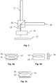
- a confocal device of the invention With reference to Fig. 1 , a confocal device of the invention will be described.
- the device of the invention comprises a broadband light source 14.
- the light source 14 may comprise, for instance, a thermal source (halogen for instance), an array of LEDs, or a supercontinuum light source for instance.
- the light source 14 is optically connected, for instance by an optical fiber 24, to a first optical integrated circuit 11.
- This first integrated circuit 11 comprises a plurality of achromatic emission channel waveguides 12 and Y-junctions 28 guiding the light of the light source 14 towards an array of emitting apertures 29, made on an edge of the first optical integrated circuit 11 by terminating end of emission channel waveguides 12.
- the light exiting these emitting apertures 29 forms the optical measurement channels 13.
- the emission channel waveguides 12 are single-mode within the spectral range of the source (used spectral range). They connect cascaded Y-junctions 28 which split the light of the source 14 between the emitting apertures 29. In Fig. 1 , only the first and the last stages of the cascade of Y-junctions is shown for sake of clarity.
- the emission channel waveguides 12 and the Y-junctions 28 are substantially achromatic within the spectral range of the source, which means notably that the coupling ratio of the Y-junctions 28 is little or not dependent on the wavelength.
- the light of the optical measurement channels 13 After exiting the emitting apertures 29, the light of the optical measurement channels 13 passes through a beam splitter cube 22, and is directed to a focusing lens 10.
- the focusing lens arrangement 10 may comprise, as illustrated on FIG. 3a , a collimating lens element 30 and a chromatic lens element 31.
- the focusing lens arrangement 10 with the chromatic lens element 31 is designed according to well-known techniques so as to provide a strong chromatic aberration, allowing different optical wavelengths crossing the lens to be focused at different axial distances, i.e. distances along the optical axis of the lens, or along the Z axis as shown in Figure 1 .
- the light of the respective optical measurement channels 13 is focused by the focusing lens arrangement 10 on an array of respective measurement points 15, or more precisely, thanks to the chromatic lens element 31, along a measurement line 15 in the axial direction of the lens (z-axis in Fig. 1 ) depending on the wavelengths.
- the range at which the respective wavelengths of the light source 14 are focused defines the chromatic measurement range.
- the wavelengths focused on that interface for the respective optical measurement channels 13 are reflected and directed by the beam splitter 22 to collection apertures 18 defined by optical channel waveguides 19 fabricated in a second integrated optics circuit 20.
- Emitting apertures 29 and collection apertures 18 are optical conjugate of the measurement points 15 for the chromatic focusing lens arrangement 10 only at wavelengths focused on the interface of the object 17.
- the second integrated optics circuit 20 comprises detection channel waveguides 19, with an entrance end on an edge of the second integrated optics circuit 20 forming the emitting apertures 29. These detection channel waveguides direct the collected reflected light towards optical detectors 25 facing an edge of the second integrated optics circuit 20.
- optical detectors 25 may comprise spectral detectors to create an intensity spectrum of the light issued from each detection channel waveguides 19.
- Such spectral detectors may comprise a first lens for collimating the incoming light issued from the detection channel waveguides 19, a dispersing element such as prisms, a diffraction array or a grating for dispersing angularly the different wavelengths of the incoming light, a second lens and a linear or matrixial detector such as a CCD for re-imaging the dispersed light so that different wavelengths are focused on different pixels of the sensor, and a pixel provides a measurement of light intensity at a specific wavelength or within a limited range of wavelength.
- a dispersing element such as prisms, a diffraction array or a grating for dispersing angularly the different wavelengths of the incoming light
- a second lens and a linear or matrixial detector such as a CCD for re-imaging the dispersed light so that different wavelengths are focused on different pixels of the sensor, and a pixel provides a measurement of light intensity at a specific wavelength or within a limited
- Spectral sensors may also comprise color sensors with color filters applied on an array or a matrix of pixels of a CCD or a CMOS sensor, so that a pixel provides a measurement of light intensity at a specific wavelength or within a limited range of wavelength.
- the intensity spectrum of the light is also obtained by collecting the information on the pixels of the sensor. An intensity spectrum is produced for each detection channel waveguide 19.
- a separate CCD or CMOS array may be used for collecting the light of each different detection channel waveguide 19. But preferably, the light from all or at least a plurality of detection channel waveguides 19 is directed towards a CCD or CMOS matrix, the wavelengths or the colors being dispersed along one direction of the matrix.
- an interface of the object 17 present in the measurement range gives rise to a peak in the intensity spectrum around the wavelength focused at the corresponding axial position.
- the intensity spectrum is analyzed to obtain an axial distance information, or the position of the interfaces or the surface of the object 17 within the measurement range. So, a 3D profile of the object 17 is obtained along the array of optical measurement channels 13.
- a 3D image can be obtained by scanning the surface of the object with the sensor.
- optical detectors 25 may also comprise intensity detectors for fast 2D imaging.
- Such detectors comprise a CCD or a CMOS sensor (for instance) with an array or a matrix of pixels. As there is no dispersing element, in that configuration a pixel of the sensor collects the whole light over the full spectrum of the light issued from a detection channel waveguide 19.
- the light from all or at least a plurality of detection channel waveguides 19 is directed towards a same CCD or CMOS array (line sensor) or matrix.
- a 2D intensity or gray level line of the object 17 is obtained along the array of optical measurement channels 13, with an optimal lateral resolution over an extended depth of focus.
- a 2D image can be obtained by scanning the surface of the object with the sensor.
- optical detectors 25 can comprise simultaneously spectral detectors and intensity detectors, for instance on different optical measurement channels 13, for acquiring simultaneously 2D and 3D information.
- the optical detectors 25 may be interfaced with the integrated optics circuits 11, 20 either directly, with the optical detector entrance or sensor facing the end of the detection channel waveguides, or using known interfacing method such as fiber optics 24, V-groove, butt-coupling, microlenses and/or tapers in waveguides, in particular compatible with well automated methods and low coupling power loss.
- Detection channel waveguides 19 are preferably designed for allowing multimode propagation. This allows to have them made with a larger cross-section area and larger acceptance angle at the collection apertures 18 so as to maximize the collection of the reflected light from measured points 15 and also minimize the crosstalk due to reflected light captured by adjacent detecting channels.
- the detection channel waveguides 19 are further built with an angled (90 degrees) or curved design so as to direct any light not coupled into the detection channel waveguides 19 away from the optical detector 25.
- the detection channel waveguides 19 are arranged so that the optical detectors 25 are out-of-sight of the stray light coupled at the collection apertures 18 level.
- angles design of the detection channel waveguides 19 allows integrating optical detectors 25 on two sides of the second integrated optics circuit 20 as illustrated on Fig. 1 .
- some other modes of realization may implement optical detectors 25 on a single side of the second integrated circuit 20.
- the second (detection) integrated optics circuit 20 may be built and arranged so as to fulfill the following characteristics and requirements:
- the detection channel waveguides 19 may be arranged on the detector side to match the pitch of the optical detector 25 pixels and the optical apertures of these optical detectors 25, or the entrance optics of these optical detectors 25.
- the detection channel waveguides 19 may be arranged with a pitch and a numerical aperture so as to match the detector pixel pitch in the same way through that imaging stage.
- detection channel waveguides 19 When using spectral detector, it is desirable to have the light issued from different detection channel waveguides 19 and spectrally dispersed projected on different rows of pixels of the optical detector 25, to avoid cross-talk. This may also be achieved by providing detection channel waveguides 19 with a pitch at their exit side for instance corresponding to twice the detector pixel pitch (to have one row of pixel over two used for cross-talk isolation). Of course, as previously, the imaging entrance stage of the optical detectors 25 has to be taken into account.
- the sensor of the invention further comprises means for control and data processing such as computer, microcontroller and/or FPGA modules 23, connected to the optical detectors 25.
- the first and second integrated optics circuits 11 and 20 are aligned relatively to each other and to the focusing lens 10, and are made to stay permanently in close contact with the beam splitter 22.
- the first and second integrated optics circuits 11 and 20 are bounded or glued to the beam splitter 22 so as to form a single piece or monolithic arrangement.
- a method for doing the permanent connection is to use an optical adhesive in or around the optical paths.
- a mechanically robust and optically stable device is then manufactured.
- Alignment optical channel waveguides 26, 27 can be added respectively to the first integrated optics circuit 11 and to the second integrated optics circuit 20 in order to provide alignment means. Those alignment optical channel waveguides 26, 27 can be coupled permanently or temporarily to optical fibers guiding the light from a pilot light and/or to a monitoring device (power meter or camera for examples).
- a first set of alignment waveguides 26 is used to align the first integrated optics circuit 11 in the focal plane (or an imaging plane) of the focusing lens 10.
- These first alignment waveguides 26 are arranged on both sides of the emission channel waveguides 12 and have an emitting aperture located close to the emitting apertures 29 of these emission channel waveguides 12.
- first step of alignment light is injected in these first alignment waveguides 26 towards the focusing lens arrangement 10 and a reference object 17 or mirror placed at a reference position or a conjugate plane of the focusing lens arrangement 10. Reflected light is collected back in these first alignment waveguides 26.
- the relative positioning of the focusing lens arrangement 10 and the first integrated optics circuit 11 is adjusted by optimizing this coupling.
- a second set of alignment waveguides 27 on the second integrated optics circuit 20 is used to align this second integrated optics circuit 20 relative to the first integrated optics circuit 11.
- These second alignment waveguides 27 have collection apertures 18 designed to be in confocal arrangement with the emitting apertures of the first alignment waveguides 12 through the focusing lens arrangement 10.
- a second step of alignment light is injected in the first alignment waveguides 26 towards the focusing lens arrangement 10 and a reference object 17 or mirror placed at a reference position or a conjugate plane of the focusing lens arrangement 10.
- the second integrated optics circuit 20 is then positioned so as to optimize the reflected light coupled in the second alignment waveguides 27.
- the relative alignment of the first integrated optics circuit 11, the second integrated optics circuit 20, the beam slitter cube 22 and the focusing lens arrangement 10 is achieved. All pieces can be fixed together.
- optical detectors 25 can be aligned relative to the optical detection channel waveguides 19 using the light propagated in these detection channel waveguides 19.
- the alignment optical channel waveguides 26, 27 can also be used to automate the device assembly process.
- the first and second integrated optics circuits 11, 20 may be done with several techniques to produce optical waveguides, which are areas with a higher index of refraction embedded in a transparent substrate with a lower index of refraction.
- the integrated optics circuits may be done using an ion exchange process on a glass substrate. Such ion exchange occurs between a glass substrate and a molten salt bath when these are suitably brought into contact. This phenomenon locally increases the optical index of the glass by modifying its composition.
- a thin metal layer is deposited on a glass substrate. Openings with a size of a few microns to a few tens of microns, with designs corresponding to waveguides, Y-junctions and other components, are opened in the metallic layer using a classical photolithography technique.
- a one-step or two-steps ion-exchange process may be implemented to create the waveguides on, or below, the glass surface.
- the first step consists in diffusing at high temperature ions such as silver or potassium ions into the glass wafer using a molten salt bath, so as to create surface waveguides.
- an electric field may be applied for moving the ions and thus the waveguides deeper into the glass.
- the integrated optics component may also be done using techniques involving deposition of layers of doped silica or other materials on wafers for constituting waveguides.
- the deposition steps usually involve CVD techniques.
- the integrated optics component may also be done using direct inscription techniques.
- the waveguides may be done by modifying locally the index of refraction of a sol-gel substrate or a polymer resin with a UV laser beam, by photo-polymerization.
- a Y-junction as used in the invention may comprise a first waveguide which is enlarged progressively in a tapered zone (or a taper) ending in two branching waveguides.
- the tapered zone is preferably smooth enough to allow an adiabatic transition with a spread of the spatial modes of the guided light issued from the first waveguide, which are coupled in the branching waveguides.
- Such arrangement has the advantage of being essentially achromatic over a broad spectral range. So, a fixed split ratio (for instance 50/50) may be obtained over such broad spectral range.
- the first integrated optics circuit 11, the second integrated optics circuit 20 and the beam splitter 22 may be arranged so that the first integrated circuit 11 and the second integrated optics circuit 20 are facing orthogonal faces of the beam splitter 22 (as in the configuration of Fig. 1 ), but are also arranged so that their waveguide planes are orthogonal to each other (while in the arrangement of Fig. 1 the waveguide planes of these integrated circuit are parallel to each other or in the same plane).
- Such configuration has the advantage of requiring a much smaller beam splitter cube 22, which may be for instance in the shape of an elongated bar.
- the device of the invention has been described for a chromatic confocal configuration.
- the device of the invention may implement a confocal detection scheme. In that case:
- the device may further comprise a Z-scanning stage 34 to move relatively the sensor and the object 17 along the Z axis.
- the height of the surface of the object 17 may then be obtained at the measurement points from the position of the Z-scanning stage 34 for which a maximum of intensity is obtained on the intensity optical detectors 25.
- the device of the invention may implement an interferometric detection scheme based on a low-coherence interferometry technique.
- a low-coherence interferometry technique in the spectral domain may be implemented.
- a low-coherence interferometry technique in the spectral domain may be implemented.
- the intensity spectrum of the light as obtained by the spectral optical detectors 25 is modulated by the interferences between beams reflected by the reference plate 32, and/or interfaces of the object 17.
- the height between the reference plate 32 and the object 17, and/or the thickness of layers of the object 17 may be obtained from that intensity spectrum using well-known techniques.
- a low-coherence interferometry technique with a swept source may be implemented.
- a low-coherence interferometry technique with a swept source may be implemented.
- an intensity spectrum of the light as obtained by sweeping the frequency of the light source 14 over a frequency range and acquiring the light intensity for each frequency with the intensity light detectors 25.
- the height between the reference plate 32 and the object 17, and/or the thickness of layers of the object 17 may be obtained from that intensity spectrum using well-known techniques.
Landscapes
- Physics & Mathematics (AREA)
- General Physics & Mathematics (AREA)
- Engineering & Computer Science (AREA)
- Microelectronics & Electronic Packaging (AREA)
- Optics & Photonics (AREA)
- Health & Medical Sciences (AREA)
- General Health & Medical Sciences (AREA)
- Nuclear Medicine, Radiotherapy & Molecular Imaging (AREA)
- Radiology & Medical Imaging (AREA)
- Microscoopes, Condenser (AREA)
- Investigating Or Analysing Materials By Optical Means (AREA)
- Length Measuring Devices By Optical Means (AREA)
Claims (18)
- Capteur confocal multicanal comportant au moins une source de lumière (14), au moins un agencement de lentilles de focalisation (10), au moins un détecteur optique (25), et comprenant par ailleurs :- un premier circuit optique intégré (11) agencé pour diviser un faisceau lumineux (24) en provenance de ladite au moins une source de lumière (14) en une pluralité de faisceaux lumineux émis appliqués sur un réseau à haute densité d'ouvertures d'émission (29),- un deuxième circuit optique intégré (20) agencé pour collecter sur une pluralité d'ouvertures de collecte (18) une pluralité de faisceaux lumineux réfléchis en provenance d'un échantillon (17) destiné à être inspecté et pour transférer lesdits faisceaux lumineux réfléchis audit au moins un détecteur optique (25),- un diviseur de faisceau (22) agencé (i) pour diriger lesdits faisceaux lumineux émis en provenance dudit premier circuit optique intégré (11) sur ledit échantillon inspecté (17) au travers dudit au moins un agencement de lentilles de focalisation (10) et (ii) pour diriger lesdits faisceaux lumineux réfléchis en provenance dudit échantillon inspecté (17) au travers dudit au moins un agencement de lentilles de focalisation (10) jusque dans ledit deuxième circuit optique intégré (20),ledit premier circuit optique intégré (11) comprenant des réseaux de guides d'ondes de canaux d'émission (12), dans lequel lesdits guides d'ondes de canaux d'émission (12) comprennent des guides d'ondes monomode dans le domaine spectral de la source de lumière (14).
- Capteur selon la revendication 1, dans lequel le premier circuit optique intégré (11) comprend des réseaux de guides d'ondes de canaux d'émission (12) sensiblement achromatiques dans le domaine spectral de la source de lumière (14), et ayant une extrémité formant les ouvertures d'émission (29).
- Capteur selon la revendication 2, dans lequel le premier circuit optique intégré (11) comprend en outre des diviseurs de jonctions en Y sensiblement achromatiques dans le domaine spectral de la source de lumière (14).
- Capteur selon la revendication 2 ou 3, dans lequel le deuxième circuit optique intégré (20) comprend des réseaux de guides d'ondes de canaux de détection optiques (19) sensiblement achromatiques dans le domaine spectral de la source de lumière (14), et ayant une première extrémité formant les ouvertures de collecte (18).
- Capteur selon la revendication 4, dans lequel les guides d'ondes de canaux de détection optiques (19) et les guides d'ondes de canaux d'émission optique (12) ont un même espacement, respectivement, du côté des ouvertures de collecte (18) et du côté des ouvertures d'émission (29).
- Capteur selon la revendication 4 ou 5, dans lequel les guides d'ondes de canaux de détection optiques (19) ont un diamètre supérieur par rapport au diamètre des guides d'ondes de canaux d'émission optique (12).
- Capteur selon l'une quelconque des revendications 4 à 6, dans lequel les guides d'ondes de canaux de détection optiques (19) ont un angle d'acceptation supérieur du côté des ouvertures de collecte (18) par rapport à l'angle d'acceptation des guides d'ondes de canaux d'émission optique (12) du côté des ouvertures d'émission (29).
- Capteur selon l'une quelconque des revendications 6 ou 7, dans lequel les guides d'ondes de canaux de détection (19) comprennent des guides d'ondes multimode, dans le domaine spectral de la source de lumière (14).
- Capteur selon l'une quelconque des revendications 4 à 8, dans lequel les guides d'ondes de canaux de détection (19) sont conçus pour correspondre à une deuxième extrémité à l'ouverture et/ou au pas de pixel d'éléments de détection dudit au moins un détecteur optique (25), directement ou dans un plan conjugué.
- Capteur selon l'une quelconque des revendications 4 à 9, dans lequel les guides d'ondes de canaux de détection (19) sont agencés de telle sorte que ledit au moins un détecteur optique (25) est hors de vue de la lumière parasite couplée dans le deuxième circuit intégré entre les guides d'ondes de canaux de détection (19) au niveau des ouvertures de collecte (18).
- Capteur selon l'une quelconque des revendications précédentes, dans lequel au moins l'un parmi les premier et deuxième circuits optiques intégrés (11, 20) comprend des guides d'ondes de type plan sur un substrat plan.
- Capteur selon la revendication 11, comprenant des premier et deuxième circuits optiques intégrés (11, 20) réalisés sur des substrats plans agencés avec un bord orienté respectivement vers un côté du diviseur de faisceau (22) sous la forme d'un cube de diviseur de faisceau.
- Capteur selon l'une quelconque des revendications précédentes, dans lequel les premier et deuxième circuits optiques intégrés comprennent par ailleurs des guides d'ondes de canaux optiques d'alignement.
- Capteur selon l'une quelconque des revendications précédentes, dans lequel les premier et deuxième circuits optiques intégrés (11, 20) et le diviseur de faisceau (22) sont fixés de manière permanente les uns par rapport aux autres.
- Capteur selon l'une quelconque des revendications précédentes, dans lequel l'agencement de lentilles de focalisation (10) comporte une lentille chromatique avec un chromatisme axial étendu.
- Capteur selon l'une quelconque des revendications précédentes, dans lequel ledit au moins un détecteur optique (25) comprend l'un des capteurs suivants :- un détecteur optique d'intensité avec un réseau ou une matrice de pixels ou d'éléments de détection, les pixels recevant respectivement la lumière, sur l'ensemble de son spectre, collectée par une seule ouverture de collecte (18) ;- un détecteur optique spectral avec un élément filtrant ou spectralement dispersant et un réseau ou une matrice de pixels ou d'éléments de détection, les pixels recevant respectivement la lumière, sur une sous-partie de son spectre, collectée par une seule ouverture de collecte (18).
- Procédé d'inspection d'un échantillon (17), mis en œuvre dans un capteur confocal multicanal selon l'une quelconque des revendications précédentes, comprenant les étapes consistant à :- émettre un faisceau lumineux en provenance d'au moins une source de lumière (14),- diviser ledit faisceau lumineux en une pluralité de faisceaux lumineux émis,- diriger ladite pluralité de faisceaux lumineux émis, au travers d'un agencement de lentilles de focalisation (10), jusque sur ledit échantillon inspecté (17),- collecter des faisceaux lumineux réfléchis en provenance dudit échantillon inspecté (17) au travers dudit agencement de lentilles de focalisation (10), et- diriger lesdits faisceaux lumineux réfléchis collectés jusqu'à au moins un détecteur optique (25),caractérisé en ce que :- ladite étape consistant à diviser est mise en œuvre dans un premier circuit optique intégré (11),- ladite étape consistant à collecter est mise en œuvre dans un deuxième circuit optique intégré (20), et- lesdites étapes consistant à diriger sont mises en œuvre dans un diviseur de faisceau (22).
- Procédé selon la revendication 17, comprenant par ailleurs les étapes suivantes consistant à :- faire varier la hauteur du capteur par rapport à l'échantillon (14) ; et en utilisant un agencement de lentilles de focalisation achromatiques (10) et un détecteur optique d'intensité (25), détecter l'intensité sur le spectre tout entier de faisceaux lumineux réfléchis collectés ; ou- en utilisant un agencement de lentilles de focalisation achromatiques (10) et un détecteur optique spectral (25), détecter des spectres de faisceaux lumineux réfléchis collectés ; ou- en utilisant un agencement de lentilles de focalisation chromatiques (10) et un détecteur optique spectral (25), détecter des spectres de faisceaux lumineux réfléchis collectés ;- en utilisant un agencement de lentilles de focalisation chromatiques (10) et un détecteur d'intensité (25), détecter l'intensité sur le spectre tout entier de faisceaux lumineux réfléchis collectés.
Priority Applications (3)
| Application Number | Priority Date | Filing Date | Title |
|---|---|---|---|
| EP17305967.6A EP3431918B1 (fr) | 2017-07-20 | 2017-07-20 | Capteur confocal multicanal et procédé associé permettant d'inspecter un échantillon |
| CN201880048331.9A CN110945316B (zh) | 2017-07-20 | 2018-07-16 | 用于检查样品的多通道共焦传感器和相关方法 |
| PCT/EP2018/069291 WO2019016151A1 (fr) | 2017-07-20 | 2018-07-16 | Capteur confocal multicanal et procédé associé pour inspecter un échantillon |
Applications Claiming Priority (1)
| Application Number | Priority Date | Filing Date | Title |
|---|---|---|---|
| EP17305967.6A EP3431918B1 (fr) | 2017-07-20 | 2017-07-20 | Capteur confocal multicanal et procédé associé permettant d'inspecter un échantillon |
Publications (2)
| Publication Number | Publication Date |
|---|---|
| EP3431918A1 EP3431918A1 (fr) | 2019-01-23 |
| EP3431918B1 true EP3431918B1 (fr) | 2021-03-31 |
Family
ID=60191298
Family Applications (1)
| Application Number | Title | Priority Date | Filing Date |
|---|---|---|---|
| EP17305967.6A Active EP3431918B1 (fr) | 2017-07-20 | 2017-07-20 | Capteur confocal multicanal et procédé associé permettant d'inspecter un échantillon |
Country Status (3)
| Country | Link |
|---|---|
| EP (1) | EP3431918B1 (fr) |
| CN (1) | CN110945316B (fr) |
| WO (1) | WO2019016151A1 (fr) |
Families Citing this family (8)
| Publication number | Priority date | Publication date | Assignee | Title |
|---|---|---|---|---|
| CN115079340B (zh) * | 2017-05-12 | 2024-02-02 | 周超 | 使用低损耗集成光子芯片的空分复用光学相干层析成像技术 |
| CN111487038B (zh) * | 2020-04-23 | 2022-04-08 | 华侨大学 | 一种集成微色散透镜阵列面板和并行彩色共聚焦测量系统 |
| CN111412863B (zh) * | 2020-04-23 | 2021-10-22 | 华侨大学 | 一种并行彩色共聚焦三维形貌光学测量系统 |
| CN111426287A (zh) * | 2020-04-23 | 2020-07-17 | 华侨大学 | 一种并行彩色共聚焦平面度测量系统 |
| FR3118175A1 (fr) * | 2020-12-18 | 2022-06-24 | Unity Semiconductor | Procede d’inspection d’une surface d’un objet |
| US20220390510A1 (en) * | 2021-06-03 | 2022-12-08 | UTAC Headquarters Pte. Ltd. | Illuminator Method and Device for Semiconductor Package Testing |
| CN118355257A (zh) * | 2022-04-11 | 2024-07-16 | 歌尔光学科技有限公司 | 波导测量装置 |
| CN115900590B (zh) * | 2023-02-16 | 2023-06-13 | 武汉加特林光学仪器有限公司 | 一种高信噪比的光谱共焦三维检测系统及方法 |
Citations (2)
| Publication number | Priority date | Publication date | Assignee | Title |
|---|---|---|---|---|
| US9494529B1 (en) * | 2016-03-25 | 2016-11-15 | Fogale Nanotech | Chromatic confocal device and method for 2D/3D inspection of an object such as a wafer with variable spatial resolution |
| US20160357007A1 (en) * | 2015-05-05 | 2016-12-08 | Eric Swanson | Fixed distal optics endoscope employing multicore fiber |
Family Cites Families (11)
| Publication number | Priority date | Publication date | Assignee | Title |
|---|---|---|---|---|
| FR2725795A1 (fr) * | 1994-10-13 | 1996-04-19 | Corning Inc | Dispositif achromatique en optique integree |
| FR2764376B1 (fr) * | 1997-06-04 | 1999-07-16 | Commissariat Energie Atomique | Dispositif integre de lecture des raies spectrales contenues dans un spectre optique |
| WO2005103775A1 (fr) * | 2004-04-19 | 2005-11-03 | Hitachi Chemical Company, Ltd. | Guide d’ondes optique incurve du type en forme de s et dispositif optique |
| JP2005338467A (ja) * | 2004-05-27 | 2005-12-08 | Nhk Spring Co Ltd | 光分岐器及びその製造方法 |
| CN100399079C (zh) * | 2004-07-02 | 2008-07-02 | 日本电信电话株式会社 | 光学功能回路 |
| TWI414817B (zh) | 2010-07-23 | 2013-11-11 | Univ Nat Taipei Technology | 線型彩色共焦顯微系統 |
| TWI434022B (zh) * | 2011-11-29 | 2014-04-11 | Univ Nat Taipei Technology | 彩色共焦顯微系統及其訊號處理方法 |
| EP2929329B1 (fr) * | 2012-12-10 | 2020-05-06 | Uster Technologies AG | Dispositif pour le contrôle optique d'un textile en mouvement |
| FR3006758B1 (fr) * | 2013-06-05 | 2016-05-06 | Asentys Sas | Dispositif optique integre de mesure sans contact d'altitudes et d'epaisseurs |
| AU2015367283B2 (en) * | 2014-12-14 | 2021-05-20 | Cylite Pty Ltd | Multichannel optical receivers |
| CN105629380B (zh) * | 2016-03-16 | 2018-11-20 | 天津大学 | 用于色散控制的芯片上集成的光波导结构及色散控制方法 |
-
2017
- 2017-07-20 EP EP17305967.6A patent/EP3431918B1/fr active Active
-
2018
- 2018-07-16 WO PCT/EP2018/069291 patent/WO2019016151A1/fr active Application Filing
- 2018-07-16 CN CN201880048331.9A patent/CN110945316B/zh active Active
Patent Citations (2)
| Publication number | Priority date | Publication date | Assignee | Title |
|---|---|---|---|---|
| US20160357007A1 (en) * | 2015-05-05 | 2016-12-08 | Eric Swanson | Fixed distal optics endoscope employing multicore fiber |
| US9494529B1 (en) * | 2016-03-25 | 2016-11-15 | Fogale Nanotech | Chromatic confocal device and method for 2D/3D inspection of an object such as a wafer with variable spatial resolution |
Also Published As
| Publication number | Publication date |
|---|---|
| CN110945316B (zh) | 2021-11-09 |
| WO2019016151A1 (fr) | 2019-01-24 |
| EP3431918A1 (fr) | 2019-01-23 |
| CN110945316A (zh) | 2020-03-31 |
Similar Documents
| Publication | Publication Date | Title |
|---|---|---|
| EP3431918B1 (fr) | Capteur confocal multicanal et procédé associé permettant d'inspecter un échantillon | |
| CN109073367B (zh) | 集成彩色共焦传感器 | |
| EP3222965B1 (fr) | Dispositif et procédé confocal chromatique avec résolution spatiale variable pour l'inspection en 2d/3d d'un objet tel qu'une plaquette | |
| CN113064236B (zh) | 用于自由空间光耦合的集成装置及系统 | |
| EP3634203B1 (fr) | Tomographie par cohérence optique à multiplexage par division d'espace au moyen d'un dispositif photonique intégré | |
| CN107209356B (zh) | 用于高度和厚度的非接触式测量的集成光学器件 | |
| WO2012172968A1 (fr) | Dispositif optique | |
| US6160943A (en) | Multiple-core optical fibers and associated coupling methods | |
| Xu et al. | 3D-printed facet-attached microlenses for advanced photonic system assembly | |
| US11982851B2 (en) | Alignment and readout of optical chips | |
| WO2012118021A1 (fr) | Guide d'onde optique, dispositif d'irradiation par faisceau laser, et procédé de montage d'un dispositif d'irradiation par faisceau laser. | |
| CN116068695A (zh) | 一种集成光电子空分复用光学相干层析成像光波导芯片 | |
| JP5016009B2 (ja) | 光信号処理装置およびその組み立て方法 | |
| JP6714555B2 (ja) | 光導波路部品、コアの調芯方法、および光素子の実装方法 | |
| TWI301540B (fr) | ||
| CN118130046A (zh) | 一种贝塞尔结构光照明的特种光纤系统及在线检测方法 | |
| KR20100054902A (ko) | 광분할기가 없는 피드백 광로를 갖는 센서일체형 광섬유 커플링 장치 |
Legal Events
| Date | Code | Title | Description |
|---|---|---|---|
| STAA | Information on the status of an ep patent application or granted ep patent |
Free format text: STATUS: UNKNOWN |
|
| PUAI | Public reference made under article 153(3) epc to a published international application that has entered the european phase |
Free format text: ORIGINAL CODE: 0009012 |
|
| STAA | Information on the status of an ep patent application or granted ep patent |
Free format text: STATUS: THE APPLICATION HAS BEEN PUBLISHED |
|
| AK | Designated contracting states |
Kind code of ref document: A1 Designated state(s): AL AT BE BG CH CY CZ DE DK EE ES FI FR GB GR HR HU IE IS IT LI LT LU LV MC MK MT NL NO PL PT RO RS SE SI SK SM TR |
|
| AX | Request for extension of the european patent |
Extension state: BA ME |
|
| STAA | Information on the status of an ep patent application or granted ep patent |
Free format text: STATUS: REQUEST FOR EXAMINATION WAS MADE |
|
| STAA | Information on the status of an ep patent application or granted ep patent |
Free format text: STATUS: EXAMINATION IS IN PROGRESS |
|
| 17P | Request for examination filed |
Effective date: 20190704 |
|
| RBV | Designated contracting states (corrected) |
Designated state(s): AL AT BE BG CH CY CZ DE DK EE ES FI FR GB GR HR HU IE IS IT LI LT LU LV MC MK MT NL NO PL PT RO RS SE SI SK SM TR |
|
| 17Q | First examination report despatched |
Effective date: 20190806 |
|
| GRAP | Despatch of communication of intention to grant a patent |
Free format text: ORIGINAL CODE: EPIDOSNIGR1 |
|
| STAA | Information on the status of an ep patent application or granted ep patent |
Free format text: STATUS: GRANT OF PATENT IS INTENDED |
|
| INTG | Intention to grant announced |
Effective date: 20201109 |
|
| GRAS | Grant fee paid |
Free format text: ORIGINAL CODE: EPIDOSNIGR3 |
|
| GRAA | (expected) grant |
Free format text: ORIGINAL CODE: 0009210 |
|
| STAA | Information on the status of an ep patent application or granted ep patent |
Free format text: STATUS: THE PATENT HAS BEEN GRANTED |
|
| AK | Designated contracting states |
Kind code of ref document: B1 Designated state(s): AL AT BE BG CH CY CZ DE DK EE ES FI FR GB GR HR HU IE IS IT LI LT LU LV MC MK MT NL NO PL PT RO RS SE SI SK SM TR |
|
| REG | Reference to a national code |
Ref country code: GB Ref legal event code: FG4D Ref country code: CH Ref legal event code: EP |
|
| REG | Reference to a national code |
Ref country code: AT Ref legal event code: REF Ref document number: 1377410 Country of ref document: AT Kind code of ref document: T Effective date: 20210415 |
|
| REG | Reference to a national code |
Ref country code: DE Ref legal event code: R096 Ref document number: 602017035608 Country of ref document: DE |
|
| REG | Reference to a national code |
Ref country code: IE Ref legal event code: FG4D |
|
| RAP2 | Party data changed (patent owner data changed or rights of a patent transferred) |
Owner name: UNITY SEMICONDUCTOR |
|
| REG | Reference to a national code |
Ref country code: DE Ref legal event code: R081 Ref document number: 602017035608 Country of ref document: DE Owner name: UNITY SEMICONDUCTOR, FR Free format text: FORMER OWNER: FOGALE NANOTECH, NIMES, FR |
|
| REG | Reference to a national code |
Ref country code: LT Ref legal event code: MG9D |
|
| PG25 | Lapsed in a contracting state [announced via postgrant information from national office to epo] |
Ref country code: BG Free format text: LAPSE BECAUSE OF FAILURE TO SUBMIT A TRANSLATION OF THE DESCRIPTION OR TO PAY THE FEE WITHIN THE PRESCRIBED TIME-LIMIT Effective date: 20210630 Ref country code: NO Free format text: LAPSE BECAUSE OF FAILURE TO SUBMIT A TRANSLATION OF THE DESCRIPTION OR TO PAY THE FEE WITHIN THE PRESCRIBED TIME-LIMIT Effective date: 20210630 Ref country code: HR Free format text: LAPSE BECAUSE OF FAILURE TO SUBMIT A TRANSLATION OF THE DESCRIPTION OR TO PAY THE FEE WITHIN THE PRESCRIBED TIME-LIMIT Effective date: 20210331 Ref country code: FI Free format text: LAPSE BECAUSE OF FAILURE TO SUBMIT A TRANSLATION OF THE DESCRIPTION OR TO PAY THE FEE WITHIN THE PRESCRIBED TIME-LIMIT Effective date: 20210331 |
|
| PG25 | Lapsed in a contracting state [announced via postgrant information from national office to epo] |
Ref country code: SE Free format text: LAPSE BECAUSE OF FAILURE TO SUBMIT A TRANSLATION OF THE DESCRIPTION OR TO PAY THE FEE WITHIN THE PRESCRIBED TIME-LIMIT Effective date: 20210331 Ref country code: RS Free format text: LAPSE BECAUSE OF FAILURE TO SUBMIT A TRANSLATION OF THE DESCRIPTION OR TO PAY THE FEE WITHIN THE PRESCRIBED TIME-LIMIT Effective date: 20210331 Ref country code: LV Free format text: LAPSE BECAUSE OF FAILURE TO SUBMIT A TRANSLATION OF THE DESCRIPTION OR TO PAY THE FEE WITHIN THE PRESCRIBED TIME-LIMIT Effective date: 20210331 |
|
| REG | Reference to a national code |
Ref country code: NL Ref legal event code: MP Effective date: 20210331 |
|
| REG | Reference to a national code |
Ref country code: AT Ref legal event code: MK05 Ref document number: 1377410 Country of ref document: AT Kind code of ref document: T Effective date: 20210331 |
|
| PG25 | Lapsed in a contracting state [announced via postgrant information from national office to epo] |
Ref country code: CZ Free format text: LAPSE BECAUSE OF FAILURE TO SUBMIT A TRANSLATION OF THE DESCRIPTION OR TO PAY THE FEE WITHIN THE PRESCRIBED TIME-LIMIT Effective date: 20210331 Ref country code: EE Free format text: LAPSE BECAUSE OF FAILURE TO SUBMIT A TRANSLATION OF THE DESCRIPTION OR TO PAY THE FEE WITHIN THE PRESCRIBED TIME-LIMIT Effective date: 20210331 Ref country code: LT Free format text: LAPSE BECAUSE OF FAILURE TO SUBMIT A TRANSLATION OF THE DESCRIPTION OR TO PAY THE FEE WITHIN THE PRESCRIBED TIME-LIMIT Effective date: 20210331 Ref country code: AT Free format text: LAPSE BECAUSE OF FAILURE TO SUBMIT A TRANSLATION OF THE DESCRIPTION OR TO PAY THE FEE WITHIN THE PRESCRIBED TIME-LIMIT Effective date: 20210331 Ref country code: NL Free format text: LAPSE BECAUSE OF FAILURE TO SUBMIT A TRANSLATION OF THE DESCRIPTION OR TO PAY THE FEE WITHIN THE PRESCRIBED TIME-LIMIT Effective date: 20210331 Ref country code: SM Free format text: LAPSE BECAUSE OF FAILURE TO SUBMIT A TRANSLATION OF THE DESCRIPTION OR TO PAY THE FEE WITHIN THE PRESCRIBED TIME-LIMIT Effective date: 20210331 |
|
| PG25 | Lapsed in a contracting state [announced via postgrant information from national office to epo] |
Ref country code: PL Free format text: LAPSE BECAUSE OF FAILURE TO SUBMIT A TRANSLATION OF THE DESCRIPTION OR TO PAY THE FEE WITHIN THE PRESCRIBED TIME-LIMIT Effective date: 20210331 Ref country code: PT Free format text: LAPSE BECAUSE OF FAILURE TO SUBMIT A TRANSLATION OF THE DESCRIPTION OR TO PAY THE FEE WITHIN THE PRESCRIBED TIME-LIMIT Effective date: 20210802 Ref country code: RO Free format text: LAPSE BECAUSE OF FAILURE TO SUBMIT A TRANSLATION OF THE DESCRIPTION OR TO PAY THE FEE WITHIN THE PRESCRIBED TIME-LIMIT Effective date: 20210331 Ref country code: SK Free format text: LAPSE BECAUSE OF FAILURE TO SUBMIT A TRANSLATION OF THE DESCRIPTION OR TO PAY THE FEE WITHIN THE PRESCRIBED TIME-LIMIT Effective date: 20210331 Ref country code: IS Free format text: LAPSE BECAUSE OF FAILURE TO SUBMIT A TRANSLATION OF THE DESCRIPTION OR TO PAY THE FEE WITHIN THE PRESCRIBED TIME-LIMIT Effective date: 20210731 |
|
| REG | Reference to a national code |
Ref country code: DE Ref legal event code: R097 Ref document number: 602017035608 Country of ref document: DE |
|
| PG25 | Lapsed in a contracting state [announced via postgrant information from national office to epo] |
Ref country code: AL Free format text: LAPSE BECAUSE OF FAILURE TO SUBMIT A TRANSLATION OF THE DESCRIPTION OR TO PAY THE FEE WITHIN THE PRESCRIBED TIME-LIMIT Effective date: 20210331 Ref country code: DK Free format text: LAPSE BECAUSE OF FAILURE TO SUBMIT A TRANSLATION OF THE DESCRIPTION OR TO PAY THE FEE WITHIN THE PRESCRIBED TIME-LIMIT Effective date: 20210331 Ref country code: ES Free format text: LAPSE BECAUSE OF FAILURE TO SUBMIT A TRANSLATION OF THE DESCRIPTION OR TO PAY THE FEE WITHIN THE PRESCRIBED TIME-LIMIT Effective date: 20210331 |
|
| PLBE | No opposition filed within time limit |
Free format text: ORIGINAL CODE: 0009261 |
|
| STAA | Information on the status of an ep patent application or granted ep patent |
Free format text: STATUS: NO OPPOSITION FILED WITHIN TIME LIMIT |
|
| REG | Reference to a national code |
Ref country code: CH Ref legal event code: PL |
|
| 26N | No opposition filed |
Effective date: 20220104 |
|
| GBPC | Gb: european patent ceased through non-payment of renewal fee |
Effective date: 20210720 |
|
| PG25 | Lapsed in a contracting state [announced via postgrant information from national office to epo] |
Ref country code: MC Free format text: LAPSE BECAUSE OF FAILURE TO SUBMIT A TRANSLATION OF THE DESCRIPTION OR TO PAY THE FEE WITHIN THE PRESCRIBED TIME-LIMIT Effective date: 20210331 |
|
| REG | Reference to a national code |
Ref country code: BE Ref legal event code: MM Effective date: 20210731 |
|
| PG25 | Lapsed in a contracting state [announced via postgrant information from national office to epo] |
Ref country code: LI Free format text: LAPSE BECAUSE OF NON-PAYMENT OF DUE FEES Effective date: 20210731 Ref country code: GB Free format text: LAPSE BECAUSE OF NON-PAYMENT OF DUE FEES Effective date: 20210720 Ref country code: CH Free format text: LAPSE BECAUSE OF NON-PAYMENT OF DUE FEES Effective date: 20210731 |
|
| PG25 | Lapsed in a contracting state [announced via postgrant information from national office to epo] |
Ref country code: IS Free format text: LAPSE BECAUSE OF FAILURE TO SUBMIT A TRANSLATION OF THE DESCRIPTION OR TO PAY THE FEE WITHIN THE PRESCRIBED TIME-LIMIT Effective date: 20210731 Ref country code: LU Free format text: LAPSE BECAUSE OF NON-PAYMENT OF DUE FEES Effective date: 20210720 |
|
| PG25 | Lapsed in a contracting state [announced via postgrant information from national office to epo] |
Ref country code: IT Free format text: LAPSE BECAUSE OF FAILURE TO SUBMIT A TRANSLATION OF THE DESCRIPTION OR TO PAY THE FEE WITHIN THE PRESCRIBED TIME-LIMIT Effective date: 20210331 Ref country code: IE Free format text: LAPSE BECAUSE OF NON-PAYMENT OF DUE FEES Effective date: 20210720 Ref country code: BE Free format text: LAPSE BECAUSE OF NON-PAYMENT OF DUE FEES Effective date: 20210731 |
|
| PG25 | Lapsed in a contracting state [announced via postgrant information from national office to epo] |
Ref country code: CY Free format text: LAPSE BECAUSE OF FAILURE TO SUBMIT A TRANSLATION OF THE DESCRIPTION OR TO PAY THE FEE WITHIN THE PRESCRIBED TIME-LIMIT Effective date: 20210331 |
|
| PG25 | Lapsed in a contracting state [announced via postgrant information from national office to epo] |
Ref country code: HU Free format text: LAPSE BECAUSE OF FAILURE TO SUBMIT A TRANSLATION OF THE DESCRIPTION OR TO PAY THE FEE WITHIN THE PRESCRIBED TIME-LIMIT; INVALID AB INITIO Effective date: 20170720 Ref country code: GR Free format text: LAPSE BECAUSE OF FAILURE TO SUBMIT A TRANSLATION OF THE DESCRIPTION OR TO PAY THE FEE WITHIN THE PRESCRIBED TIME-LIMIT Effective date: 20210331 |
|
| PG25 | Lapsed in a contracting state [announced via postgrant information from national office to epo] |
Ref country code: MK Free format text: LAPSE BECAUSE OF FAILURE TO SUBMIT A TRANSLATION OF THE DESCRIPTION OR TO PAY THE FEE WITHIN THE PRESCRIBED TIME-LIMIT Effective date: 20210331 |
|
| PG25 | Lapsed in a contracting state [announced via postgrant information from national office to epo] |
Ref country code: MT Free format text: LAPSE BECAUSE OF FAILURE TO SUBMIT A TRANSLATION OF THE DESCRIPTION OR TO PAY THE FEE WITHIN THE PRESCRIBED TIME-LIMIT Effective date: 20210331 |
|
| PGFP | Annual fee paid to national office [announced via postgrant information from national office to epo] |
Ref country code: DE Payment date: 20240828 Year of fee payment: 8 |
|
| PGFP | Annual fee paid to national office [announced via postgrant information from national office to epo] |
Ref country code: FR Payment date: 20240726 Year of fee payment: 8 |