EP3428964A1 - Semiconductor device - Google Patents
Semiconductor device Download PDFInfo
- Publication number
- EP3428964A1 EP3428964A1 EP17782549.4A EP17782549A EP3428964A1 EP 3428964 A1 EP3428964 A1 EP 3428964A1 EP 17782549 A EP17782549 A EP 17782549A EP 3428964 A1 EP3428964 A1 EP 3428964A1
- Authority
- EP
- European Patent Office
- Prior art keywords
- flow path
- path member
- semiconductor device
- circuit unit
- layer
- Prior art date
- Legal status (The legal status is an assumption and is not a legal conclusion. Google has not performed a legal analysis and makes no representation as to the accuracy of the status listed.)
- Granted
Links
Images



Classifications
-
- H—ELECTRICITY
- H10—SEMICONDUCTOR DEVICES; ELECTRIC SOLID-STATE DEVICES NOT OTHERWISE PROVIDED FOR
- H10W—GENERIC PACKAGES, INTERCONNECTIONS, CONNECTORS OR OTHER CONSTRUCTIONAL DETAILS OF DEVICES COVERED BY CLASS H10
- H10W40/00—Arrangements for thermal protection or thermal control
- H10W40/40—Arrangements for thermal protection or thermal control involving heat exchange by flowing fluids
- H10W40/47—Arrangements for thermal protection or thermal control involving heat exchange by flowing fluids by flowing liquids, e.g. forced water cooling
-
- H—ELECTRICITY
- H05—ELECTRIC TECHNIQUES NOT OTHERWISE PROVIDED FOR
- H05K—PRINTED CIRCUITS; CASINGS OR CONSTRUCTIONAL DETAILS OF ELECTRIC APPARATUS; MANUFACTURE OF ASSEMBLAGES OF ELECTRICAL COMPONENTS
- H05K7/00—Constructional details common to different types of electric apparatus
- H05K7/20—Modifications to facilitate cooling, ventilating, or heating
-
- H—ELECTRICITY
- H10—SEMICONDUCTOR DEVICES; ELECTRIC SOLID-STATE DEVICES NOT OTHERWISE PROVIDED FOR
- H10W—GENERIC PACKAGES, INTERCONNECTIONS, CONNECTORS OR OTHER CONSTRUCTIONAL DETAILS OF DEVICES COVERED BY CLASS H10
- H10W20/00—Interconnections in chips, wafers or substrates
- H10W20/40—Interconnections external to wafers or substrates, e.g. back-end-of-line [BEOL] metallisations or vias connecting to gate electrodes
-
- H—ELECTRICITY
- H10—SEMICONDUCTOR DEVICES; ELECTRIC SOLID-STATE DEVICES NOT OTHERWISE PROVIDED FOR
- H10W—GENERIC PACKAGES, INTERCONNECTIONS, CONNECTORS OR OTHER CONSTRUCTIONAL DETAILS OF DEVICES COVERED BY CLASS H10
- H10W20/00—Interconnections in chips, wafers or substrates
- H10W20/40—Interconnections external to wafers or substrates, e.g. back-end-of-line [BEOL] metallisations or vias connecting to gate electrodes
- H10W20/49—Adaptable interconnections, e.g. fuses or antifuses
-
- H—ELECTRICITY
- H10—SEMICONDUCTOR DEVICES; ELECTRIC SOLID-STATE DEVICES NOT OTHERWISE PROVIDED FOR
- H10W—GENERIC PACKAGES, INTERCONNECTIONS, CONNECTORS OR OTHER CONSTRUCTIONAL DETAILS OF DEVICES COVERED BY CLASS H10
- H10W40/00—Arrangements for thermal protection or thermal control
- H10W40/01—Manufacture or treatment
- H10W40/03—Manufacture or treatment of arrangements for cooling
- H10W40/037—Assembling together parts thereof
-
- H—ELECTRICITY
- H10—SEMICONDUCTOR DEVICES; ELECTRIC SOLID-STATE DEVICES NOT OTHERWISE PROVIDED FOR
- H10W—GENERIC PACKAGES, INTERCONNECTIONS, CONNECTORS OR OTHER CONSTRUCTIONAL DETAILS OF DEVICES COVERED BY CLASS H10
- H10W40/00—Arrangements for thermal protection or thermal control
- H10W40/20—Arrangements for cooling
- H10W40/22—Arrangements for cooling characterised by their shape, e.g. having conical or cylindrical projections
-
- H—ELECTRICITY
- H10—SEMICONDUCTOR DEVICES; ELECTRIC SOLID-STATE DEVICES NOT OTHERWISE PROVIDED FOR
- H10W—GENERIC PACKAGES, INTERCONNECTIONS, CONNECTORS OR OTHER CONSTRUCTIONAL DETAILS OF DEVICES COVERED BY CLASS H10
- H10W40/00—Arrangements for thermal protection or thermal control
- H10W40/20—Arrangements for cooling
- H10W40/231—Arrangements for cooling characterised by their places of attachment or cooling paths
-
- H—ELECTRICITY
- H10—SEMICONDUCTOR DEVICES; ELECTRIC SOLID-STATE DEVICES NOT OTHERWISE PROVIDED FOR
- H10W—GENERIC PACKAGES, INTERCONNECTIONS, CONNECTORS OR OTHER CONSTRUCTIONAL DETAILS OF DEVICES COVERED BY CLASS H10
- H10W40/00—Arrangements for thermal protection or thermal control
- H10W40/20—Arrangements for cooling
- H10W40/25—Arrangements for cooling characterised by their materials
- H10W40/255—Arrangements for cooling characterised by their materials having a laminate or multilayered structure, e.g. direct bond copper [DBC] ceramic substrates
-
- H—ELECTRICITY
- H10—SEMICONDUCTOR DEVICES; ELECTRIC SOLID-STATE DEVICES NOT OTHERWISE PROVIDED FOR
- H10W—GENERIC PACKAGES, INTERCONNECTIONS, CONNECTORS OR OTHER CONSTRUCTIONAL DETAILS OF DEVICES COVERED BY CLASS H10
- H10W40/00—Arrangements for thermal protection or thermal control
- H10W40/20—Arrangements for cooling
- H10W40/25—Arrangements for cooling characterised by their materials
- H10W40/259—Ceramics or glasses
-
- H—ELECTRICITY
- H10—SEMICONDUCTOR DEVICES; ELECTRIC SOLID-STATE DEVICES NOT OTHERWISE PROVIDED FOR
- H10W—GENERIC PACKAGES, INTERCONNECTIONS, CONNECTORS OR OTHER CONSTRUCTIONAL DETAILS OF DEVICES COVERED BY CLASS H10
- H10W40/00—Arrangements for thermal protection or thermal control
- H10W40/70—Fillings or auxiliary members in containers or in encapsulations for thermal protection or control
-
- H—ELECTRICITY
- H10—SEMICONDUCTOR DEVICES; ELECTRIC SOLID-STATE DEVICES NOT OTHERWISE PROVIDED FOR
- H10W—GENERIC PACKAGES, INTERCONNECTIONS, CONNECTORS OR OTHER CONSTRUCTIONAL DETAILS OF DEVICES COVERED BY CLASS H10
- H10W70/00—Package substrates; Interposers; Redistribution layers [RDL]
- H10W70/40—Leadframes
- H10W70/461—Leadframes specially adapted for cooling
-
- H—ELECTRICITY
- H10—SEMICONDUCTOR DEVICES; ELECTRIC SOLID-STATE DEVICES NOT OTHERWISE PROVIDED FOR
- H10W—GENERIC PACKAGES, INTERCONNECTIONS, CONNECTORS OR OTHER CONSTRUCTIONAL DETAILS OF DEVICES COVERED BY CLASS H10
- H10W70/00—Package substrates; Interposers; Redistribution layers [RDL]
- H10W70/40—Leadframes
- H10W70/481—Leadframes for devices being provided for in groups H10D8/00 - H10D48/00
-
- H—ELECTRICITY
- H10—SEMICONDUCTOR DEVICES; ELECTRIC SOLID-STATE DEVICES NOT OTHERWISE PROVIDED FOR
- H10W—GENERIC PACKAGES, INTERCONNECTIONS, CONNECTORS OR OTHER CONSTRUCTIONAL DETAILS OF DEVICES COVERED BY CLASS H10
- H10W90/00—Package configurations
-
- H—ELECTRICITY
- H10—SEMICONDUCTOR DEVICES; ELECTRIC SOLID-STATE DEVICES NOT OTHERWISE PROVIDED FOR
- H10W—GENERIC PACKAGES, INTERCONNECTIONS, CONNECTORS OR OTHER CONSTRUCTIONAL DETAILS OF DEVICES COVERED BY CLASS H10
- H10W72/00—Interconnections or connectors in packages
- H10W72/071—Connecting or disconnecting
- H10W72/072—Connecting or disconnecting of bump connectors
-
- H—ELECTRICITY
- H10—SEMICONDUCTOR DEVICES; ELECTRIC SOLID-STATE DEVICES NOT OTHERWISE PROVIDED FOR
- H10W—GENERIC PACKAGES, INTERCONNECTIONS, CONNECTORS OR OTHER CONSTRUCTIONAL DETAILS OF DEVICES COVERED BY CLASS H10
- H10W72/00—Interconnections or connectors in packages
- H10W72/071—Connecting or disconnecting
- H10W72/073—Connecting or disconnecting of die-attach connectors
-
- H—ELECTRICITY
- H10—SEMICONDUCTOR DEVICES; ELECTRIC SOLID-STATE DEVICES NOT OTHERWISE PROVIDED FOR
- H10W—GENERIC PACKAGES, INTERCONNECTIONS, CONNECTORS OR OTHER CONSTRUCTIONAL DETAILS OF DEVICES COVERED BY CLASS H10
- H10W72/00—Interconnections or connectors in packages
- H10W72/851—Dispositions of multiple connectors or interconnections
- H10W72/874—On different surfaces
- H10W72/877—Bump connectors and die-attach connectors
Definitions
- the present disclosure relates to a semiconductor device.
- a semiconductor device for high power is widely used as a power conversion device for railway vehicles, etc.
- Examples of such a semiconductor device include an inverter using semiconductor elements such as an IGBT (Insulated Gate Bipolar Transistor) and an FWD (Free Wheeling Diode).
- IGBT Insulated Gate Bipolar Transistor
- FWD Free Wheeling Diode
- Patent Literature 1 a semiconductor element is sandwiched between two lead frames, and a ceramic tube having a coolant flow path for flowing a coolant is provided on the outside of each lead frame.
- the semiconductor element and a signal line are connected by wire bonding.
- Patent Literature 1 Japanese Unexamined Patent Publication JP-A 2008-103623
- the semiconductor device of the present disclosure includes a circuit unit including a heat sink layer, a wiring layer, and a semiconductor element that is between the heat sink layer and the wiring layer; a first flow path member composed of an insulating material; and a second flow path member composed of an insulating material.
- the circuit unit is disposed between the first flow path member and the second flow path member.
- the wiring layer faces the first flow path member or the second flow path member.
- the semiconductor device of the present disclosure can efficiently cool the semiconductor element, and can also efficiently remove heat of the wiring layer for exchanging signals.
- FIG. 1 is a cross-sectional view schematically showing a first embodiment of the semiconductor device of the present disclosure.
- a circuit unit 10 including a heat sink layer 13, wiring layers 16a to 16d, and a semiconductor element 14 between the heat sink layer 13 and the wiring layers 16a to 16d is sandwiched between a first flow path member 11 and a second flow path member 21.
- the first flow path member 11 and the second flow path member 21 include coolant flow paths 12 and 22 for flowing a cooling medium (hereinafter also referred to as "coolant") inside.
- a cooling medium hereinafter also referred to as "coolant"
- any coolable liquid and gas may be used as the coolant.
- a liquid coolant pure water, Galden and the like may be used, and an antirust agent may be added.
- the circuit unit 10 can be cooled from both sides thereof.
- the wiring layers 16a to 16d face the second flow path member 21, heat generated in the wiring layers 16a to 16d during signal exchange can be efficiently removed. Therefore, in the semiconductor device 100 of the present disclosure, deterioration of the function possessed by the semiconductor element 14 is little.
- the semiconductor element 14 can be efficiently cooled via the wiring layers 16a to 16d and the heat sink layer 13.
- first flow path member 11 and the second flow path member 21 are formed of an insulating material, and thus it is possible to directly form the wiring layers 16a to 16d and the heat sink layer 13, and heat of the wiring layers 16a to 16d and the heat sink layer 13 can be delivered to the first flow path member 11 and the second flow path member 21 immediately.
- the insulating material may be ceramics such as alumina ceramics, alumina-zirconia composite ceramics, aluminum nitride ceramics, and silicon nitride ceramics.
- the silicon nitride ceramics has both excellent thermal conductivity and mechanical strength, by constituting the first flow path member 11 and the second flow path member 21 with the silicon nitride ceramics, the semiconductor device 100 of the present disclosure can have both excellent cooling efficiency and mechanical strength.
- the silicon nitride ceramics contains 70% by mass or more of silicon nitride out of 100% by mass of all components constituting the ceramics.
- the materials of the first flow path member 11 and the second flow path member 21 can be confirmed by the following method. First, measurement is performed using an X-ray diffraction apparatus (XRD), and the obtained value of 2 ⁇ (2 ⁇ is the diffraction angle) is identified with a JCPDS card. Next, quantitative analysis of each component is carried out using an ICP (Inductively Coupled Plasma) emission spectrophotometric analyzer (ICP) or an X-ray fluorescence analyzer (XRF).
- ICP Inductively Coupled Plasma
- ICP Inductively Coupled Plasma
- XRF X-ray fluorescence analyzer
- the material is a silicon nitride ceramics.
- the structures of the coolant flow paths 12 and 22 can be freely designed.
- FIG. 2A is a schematic front view of a circuit unit of the first embodiment of the semiconductor device of the present disclosure.
- FIG. 2A shows a view as seen towards the wiring layers 16a to 16d with the first flow path member 11 removed. Further, FIG. 2A shows a state in which the wiring layers 16a to 16d are connected to the semiconductor element (for example, IGBT) 14 via brazing materials or solders 15a to 15d in the four wiring layers 16a to 16d constituted in the same manner.
- the brazing materials or solders 15a to 15d which are hidden constituents, are indicated by broken lines.
- FIG. 2B is a schematic rear view of the circuit unit of the first embodiment of the semiconductor device of the present disclosure, and is a view corresponding to FIG. 2A .
- the semiconductor element 14 and part of the wiring layers 16a to 16d, which are hidden and partially hidden, are indicated by broken lines.
- FIG. 2C is a schematic view of a modified example of the circuit unit of the first embodiment of the semiconductor device of the present disclosure as seen from the side.
- a modified example 10a of FIG. 2C shows a case where a collector of the semiconductor element 14 is on the heat sink layer 13 side, a gate of the semiconductor element 14 is on the wiring layer 16a side, an emitter of the semiconductor element 14 is on the wiring layer 16e side, the collector of the semiconductor element 14 is connected to the heat sink layer 13, the gate of the semiconductor element 14 is connected to the wiring layer 16a via the brazing material or the solder 15a, and the emitter of the semiconductor element 14 is connected to the wiring layer 16e.
- the semiconductor element 14 is an IGBT
- the semiconductor element 14 can function as an IGBT power module.
- the wiring layers 16a to 16d included in the circuit unit 10 are wirings or terminals for establishing the connection with external devices, signal terminals, etc.
- the heat sink layer 13 included in the circuit unit 10 is a member for delivering heat of the semiconductor element 14 to the first flow path member 11.
- the heat sink layer 13 may also function as an electrode.
- the semiconductor element 14 is, for example, an IGBT (Insulated Gate Bipolar Transistor) or an FWD (Free Wheeling Diode), and may have another circuit element such as a capacitor and a resistor.
- the wiring layers 16a to 16d and the heat sink layer 13 included in the circuit unit 10 may be formed of metal.
- the wiring layers 16a to 16d and the heat sink layer 13 are formed of copper, copper alloy, aluminum, aluminum alloy or the like among metals, they have excellent thermal conductivity.
- the wiring layers 16a to 16d may be connected to the semiconductor element 14 via brazing materials or solders 15a to 15d.
- the heat sink layer 13 may be connected to the semiconductor element 14 via a brazing material, a solder, or a nano metal paste containing gold, silver, or copper as a main component.
- the brazing materials or the solders 15a to 15d a publicly known material may be used.
- a silver-based brazing material or a tin-based solder may be used.
- a method for forming the wiring layers 16a to 16d and the heat sink layer 13 there are a DBC (Direct Bond Copper) method or a DBA (Direct Bond Aluminum) method in which a metal plate such as a copper plate and an aluminum plate is directly adhered to the first flow path member 11 or the second flow path member 21, an AMB (Active Metal Bonding) method in which a metal plate is bonded via a silver and copper brazing material in which an active metal such as titanium, zirconium, hafnium, and niobium is added, a printing method of forming using a paste containing a metal component as a main component, a sputtering method of forming a metal layer by sputtering using titanium or chromium as an underlayer, a plating method of forming a metal layer using titanium or chromium as an underlayer, or after fine unevenness is formed, etc.
- DBC Direct Bond Copper
- DBA Direct Bond Aluminum
- AMB Active Metal Bonding
- thermal stress is not applied when a metal layer is formed on the first flow path member 11 and the second flow path member 21, and thus it is possible to obtain the semiconductor device 100 in which cracking is less prone to occur even in a long-term thermal cycle, and it is possible to enhance reliability.
- FIG. 3A is a cross-sectional view schematically showing a second embodiment of the semiconductor device of the present disclosure.
- a circuit unit 20 of a semiconductor device 200 is a unit having the same laminated structure as the circuit unit 10, and similarly, wiring layers 26a to 26d face the first flow path member 11 and are efficiently cooled.
- the circuit units 10 and 20 do not necessarily need to have the same laminated structure.
- the elements or members constituting each layer are partially different in the circuit units 10 and 20, for example, by changing the thickness of the heat sink layers 13 and 23, they may be configured so as to absorb the difference in thickness of the aforementioned elements and the like and to be fitted between the first flow path member 11 and the second flow path member 21 without causing stress distortion.
- the circuit unit 10 and the circuit unit 20 are arranged adjacent to each other with the top and bottom of one being opposite to those of the other, that is, the laminating orders are opposite as "heat sink layer ⁇ semiconductor element ⁇ wiring layer” and "wiring layer ⁇ semiconductor element ⁇ heat sink layer”.
- the first circuit unit 10 comprises the heat sink layer 13, the semiconductor element 14, and the wiring layers 16a to 16d which are arranged in this order
- the second circuit unit 20 comprises the wiring layers 26a to 26d, the semiconductor element 24, and the heat sink layer 23 which are arranged in this order.
- the wiring layers 16a to 16d and the wiring layers 26a to 26d can be efficiently cooled because they face the first flow path member 11 or the second flow path member 21. Furthermore, by arranging the adjacent circuit units 10 and 20 laminated oppositely, it is possible to balance heat and thermal stress.
- the adjacent circuit units 10 and 20 are not limited to two but also may be three, and they may be arranged in front and rear. Moreover, a plurality of circuit units may be arranged in front, rear, left and right.
- the heat sink layers 13 and 23 and the wiring layers 16a to 16d, 26a to 26d are respectively formed on the first flow path member 11 and the second flow path member 21.
- the semiconductor elements 14 and 24 are respectively bonded to the heat sink layers 13 and 23 via a brazing material, a solder, or a nano metal paste and the brazing material or the solders 15a to 15d and 25a to 25d are disposed to predetermined positions of the wiring layers 16a to 16d and 26a to 26d, the first flow path member 11 and the second flow path member 21 are laminated, and by passing through a solder reflow process, the semiconductor device 200 can be efficiently produced.
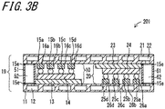
- FIG. 3B is a cross-sectional view schematically showing a third embodiment of the semiconductor device of the present disclosure.
- a semiconductor device 201 of FIG. 3B is the semiconductor device 200 of FIG. 3A provided with connecting pipes 51 and 61.
- an adhesive layer 15e is provided between opposing surfaces of the connecting pipes 51, 61 and the first flow path member 11 or the second flow path member 21.
- the adhesive layer 15e is formed by passing through a solder reflow process after applying an adhesive (for example, a silicon-based brazing material or a polyimide-based adhesive) between the connecting pipes 51, 61 and the first flow path member 11 or the second flow path member 21.
- an adhesive for example, a silicon-based brazing material or a polyimide-based adhesive
- the semiconductor device 201 of the present disclosure has the adhesive layer 15e between the opposing surfaces of the connecting pipes 51, 61 and the first flow path member 11 or the second flow path member 21.
- a part of the adhesive layer 15e may be positioned from the outer peripheral surfaces of the connecting pipes 51 and 61 to the first flow path member 11 or the second flow path member 21.
- the outer peripheral surfaces of the connecting pipes 51 and 61 are surfaces adjacent to the opposing surfaces.
- the coolant flowing through the coolant flow paths 52 and 62 can also be inhibited from leaking from between the connecting pipes 51, 61 and the first flow path member 11 or the second flow path member 21.
- FIG. 4 is a cross-sectional view schematically showing a fourth embodiment of the semiconductor device of the present disclosure.
- a semiconductor device 300 shown in FIG. 4 has a structure in which two semiconductor devices 201 of FIG. 3B are stacked vertically and further a pipe 91 for inflow of the coolant and a pipe 101 for outflow of the coolant are added, and the coolant circulates inside each coolant flow path.
- one set of cooling unit 19 is constituted with the first flow path member 11, the circuit units 10, 20, and the second flow path member 21, and similarly, another one set of cooling unit 39 is constituted with a first flow path member 31, circuit units 30, 40, and a second flow path member 41. As shown in FIG.
- the first flow path member 11 and the second flow path member 41 are members shared by the cooling units 19 and 39.
- the circuit units 30 and 40 in FIG. 4 are units having the same laminated structures as the circuit units 10 and 20. However, they do not necessarily need to have the same laminated structures.
- the cooling unit can be three-dimensionally constituted and it is possible to balance heat and stress even in this case. Further, by disposing a brazing material paste or the like at a predetermined place and performing a heat treatment or the like, it is possible to constitute a stack type power module, and it is possible to realize the semiconductor device 300 with high cooling efficiency while constituting a high density circuit.
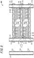
- FIG. 5 is a cross-sectional view schematically showing a fifth embodiment of the semiconductor device of the present disclosure.
- a semiconductor device 400 shown in FIG. 5 is an embodiment using a pipe in which connecting pipes are integrated. By preparing in advance a pipe 111 having a notch 112 and connecting it with the aforementioned cooling unit, it is possible to easily construct a stack type power module.
- In producing the semiconductor device 400 shown in FIG. 5 by preparing a ring-shaped spacer and arranging the spacer at a position corresponding to the notch 112 between a plurality of flow path members, it is possible to easily insert the pipe 111 positioned across the plurality of flow path members. Such a ring-shaped spacer also has an effect of preventing liquid leakage when the pipe 111 is broken.
- an adhesive for example, a silicon-based brazing material or a polyimide-based adhesive
- a solder reflow process the joining of the connecting pipes 51, 61, 71, 81, the pipes 91, 101, 111, and the ring-shaped spacer becomes possible simultaneously with soldering between the semiconductor elements and the wiring layers.
- the connecting pipes 51, 61, 71, 81, the pipes 91, 101, 111, and the ring-shaped spacer are preferably materials that can withstand the solder reflow process, for example, metal, resin, and ceramics.
- the resin polyimide is preferable.
- the resin mold a silicone gel or an epoxy resin may be used.
- the resin mold by resin-molding not only the circuit units 10, 20, 30 and 40 but also the connecting pipes 51, 61, 71, 81, the pipes 91, 101, 111, and the ring-shaped spacer, it is possible to reinforce the joint portions between the connecting pipes 51, 61, 71, 81, the pipes 91, 101, 111, the ring-shaped spacer and the first flow path members 11, 31, the second flow path members 21 and 41.
Landscapes
- Engineering & Computer Science (AREA)
- Physics & Mathematics (AREA)
- Thermal Sciences (AREA)
- Microelectronics & Electronic Packaging (AREA)
- Cooling Or The Like Of Semiconductors Or Solid State Devices (AREA)
- Chemical & Material Sciences (AREA)
- Ceramic Engineering (AREA)
- Cooling Or The Like Of Electrical Apparatus (AREA)
- Manufacturing & Machinery (AREA)
Abstract
Description
- The present disclosure relates to a semiconductor device.
- A semiconductor device for high power is widely used as a power conversion device for railway vehicles, etc. Examples of such a semiconductor device include an inverter using semiconductor elements such as an IGBT (Insulated Gate Bipolar Transistor) and an FWD (Free Wheeling Diode). In the case of a semiconductor device for high power, heating value due to switching loss or conduction loss becomes enormous, and thus it is necessary to take measures for cooling.
- For example, in the semiconductor device disclosed in Patent Literature 1, a semiconductor element is sandwiched between two lead frames, and a ceramic tube having a coolant flow path for flowing a coolant is provided on the outside of each lead frame. The semiconductor element and a signal line are connected by wire bonding.
- Patent Literature 1: Japanese Unexamined Patent Publication
JP-A 2008-103623 - The semiconductor device of the present disclosure includes a circuit unit including a heat sink layer, a wiring layer, and a semiconductor element that is between the heat sink layer and the wiring layer; a first flow path member composed of an insulating material; and a second flow path member composed of an insulating material. The circuit unit is disposed between the first flow path member and the second flow path member. The wiring layer faces the first flow path member or the second flow path member.
- Other and further objects, features, and advantages of the invention will be more explicit from the following detailed description taken with reference to the drawings wherein:
-
FIG. 1 is a cross-sectional view schematically showing a first embodiment of the semiconductor device of the present disclosure; -
FIG. 2A is a schematic front view of a circuit unit of the first embodiment of the semiconductor device of the present disclosure; -
FIG. 2B is a schematic rear view of the circuit unit of the first embodiment of the semiconductor device of the present disclosure; -
FIG. 2C is a schematic view of a modified example of the circuit unit of the first embodiment of the semiconductor device of the present disclosure as seen from the side; -
FIG. 3A is a cross-sectional view schematically showing a second embodiment of the semiconductor device of the present disclosure; -
FIG. 3B is a cross-sectional view schematically showing a third embodiment of the semiconductor device of the present disclosure; -
FIG. 4 is a cross-sectional view schematically showing a fourth embodiment of the semiconductor device of the present disclosure; and -
FIG. 5 is a cross-sectional view schematically showing a fifth embodiment of the semiconductor device of the present disclosure. - In a semiconductor device, when heat exchange is performed between a coolant flowing through a ceramic tube and a semiconductor element via a lead frame, it is possible to cool the semiconductor element. However, wire bonding, which is the wiring for exchanging signals, is not in contact with the ceramic tube, and thus the cooling of the wire bonding is insufficient. Since the wire bonding carries heat, there is a possibility of occurrence of a problem that the semiconductor element does not function properly.
- The semiconductor device of the present disclosure can efficiently cool the semiconductor element, and can also efficiently remove heat of the wiring layer for exchanging signals.
- The semiconductor device of the present disclosure will be described below with reference to the drawings. However, only constituent members necessary for explaining the features of the semiconductor device of the present disclosure are shown in each of the following drawings for reference. Therefore, the semiconductor device of the present disclosure may further include well-known constituent members not shown in each drawing.
-
FIG. 1 is a cross-sectional view schematically showing a first embodiment of the semiconductor device of the present disclosure. - In a
semiconductor device 100 shown inFIG. 1 , acircuit unit 10 including aheat sink layer 13,wiring layers 16a to 16d, and asemiconductor element 14 between theheat sink layer 13 and thewiring layers 16a to 16d is sandwiched between a firstflow path member 11 and a secondflow path member 21. - The first
flow path member 11 and the secondflow path member 21 includecoolant flow paths coolant flow paths circuit unit 10 can be cooled from both sides thereof. In thecircuit unit 10, since thewiring layers 16a to 16d face the secondflow path member 21, heat generated in thewiring layers 16a to 16d during signal exchange can be efficiently removed. Therefore, in thesemiconductor device 100 of the present disclosure, deterioration of the function possessed by thesemiconductor element 14 is little. Moreover, since theheat sink layer 13 faces the firstflow path member 11, thesemiconductor element 14 can be efficiently cooled via thewiring layers 16a to 16d and theheat sink layer 13. - In addition, the first
flow path member 11 and the secondflow path member 21 are formed of an insulating material, and thus it is possible to directly form thewiring layers 16a to 16d and theheat sink layer 13, and heat of thewiring layers 16a to 16d and theheat sink layer 13 can be delivered to the firstflow path member 11 and the secondflow path member 21 immediately. - Here, the insulating material may be ceramics such as alumina ceramics, alumina-zirconia composite ceramics, aluminum nitride ceramics, and silicon nitride ceramics. In particular, since the silicon nitride ceramics has both excellent thermal conductivity and mechanical strength, by constituting the first
flow path member 11 and the secondflow path member 21 with the silicon nitride ceramics, thesemiconductor device 100 of the present disclosure can have both excellent cooling efficiency and mechanical strength. - Here, for example, the silicon nitride ceramics contains 70% by mass or more of silicon nitride out of 100% by mass of all components constituting the ceramics. The materials of the first
flow path member 11 and the secondflow path member 21 can be confirmed by the following method. First, measurement is performed using an X-ray diffraction apparatus (XRD), and the obtained value of 2θ (2θ is the diffraction angle) is identified with a JCPDS card. Next, quantitative analysis of each component is carried out using an ICP (Inductively Coupled Plasma) emission spectrophotometric analyzer (ICP) or an X-ray fluorescence analyzer (XRF). Here, in the XRD, when the presence of silicon nitride is confirmed and the content of silicon nitride (Si3N4) converted from the content of silicon (Si) measured by ICP or XRF is 70% by mass or more, the material is a silicon nitride ceramics. The same applies to other ceramics. - As a method of constituting the first
flow path member 11 and the secondflow path member 21 with ceramics, there are an extrusion method of preparing a metallic mold and extruding a green body, a lamination method of laminating and making green sheets, etc. In the lamination method, the structures of thecoolant flow paths -
FIG. 2A is a schematic front view of a circuit unit of the first embodiment of the semiconductor device of the present disclosure.FIG. 2A shows a view as seen towards thewiring layers 16a to 16d with the firstflow path member 11 removed. Further,FIG. 2A shows a state in which thewiring layers 16a to 16d are connected to the semiconductor element (for example, IGBT) 14 via brazing materials orsolders 15a to 15d in the fourwiring layers 16a to 16d constituted in the same manner. InFIG. 2A , the brazing materials orsolders 15a to 15d, which are hidden constituents, are indicated by broken lines. - In addition,
FIG. 2B is a schematic rear view of the circuit unit of the first embodiment of the semiconductor device of the present disclosure, and is a view corresponding toFIG. 2A . InFIG. 2B , thesemiconductor element 14 and part of the wiring layers 16a to 16d, which are hidden and partially hidden, are indicated by broken lines. - Further,
FIG. 2C is a schematic view of a modified example of the circuit unit of the first embodiment of the semiconductor device of the present disclosure as seen from the side. A modified example 10a ofFIG. 2C shows a case where a collector of thesemiconductor element 14 is on theheat sink layer 13 side, a gate of thesemiconductor element 14 is on thewiring layer 16a side, an emitter of thesemiconductor element 14 is on thewiring layer 16e side, the collector of thesemiconductor element 14 is connected to theheat sink layer 13, the gate of thesemiconductor element 14 is connected to thewiring layer 16a via the brazing material or thesolder 15a, and the emitter of thesemiconductor element 14 is connected to thewiring layer 16e. When thesemiconductor element 14 is an IGBT, by providing another wiring layer on the secondflow path member 21 and connecting the another wiring layer to the collector and the emitter of thesemiconductor element 14, thesemiconductor element 14 can function as an IGBT power module. - The wiring layers 16a to 16d included in the
circuit unit 10 are wirings or terminals for establishing the connection with external devices, signal terminals, etc. Theheat sink layer 13 included in thecircuit unit 10 is a member for delivering heat of thesemiconductor element 14 to the firstflow path member 11. Theheat sink layer 13 may also function as an electrode. Thesemiconductor element 14 is, for example, an IGBT (Insulated Gate Bipolar Transistor) or an FWD (Free Wheeling Diode), and may have another circuit element such as a capacitor and a resistor. - The wiring layers 16a to 16d and the
heat sink layer 13 included in thecircuit unit 10 may be formed of metal. When the wiring layers 16a to 16d and theheat sink layer 13 are formed of copper, copper alloy, aluminum, aluminum alloy or the like among metals, they have excellent thermal conductivity. As shown inFIG. 1 , the wiring layers 16a to 16d may be connected to thesemiconductor element 14 via brazing materials or solders 15a to 15d. Similarly, although not shown in the drawing, theheat sink layer 13 may be connected to thesemiconductor element 14 via a brazing material, a solder, or a nano metal paste containing gold, silver, or copper as a main component. As the brazing materials or thesolders 15a to 15d, a publicly known material may be used. For example, a silver-based brazing material or a tin-based solder may be used. - Here, as a method for forming the wiring layers 16a to 16d and the heat sink layer 13 (hereinafter generally referred to as a metal layer in some cases), there are a DBC (Direct Bond Copper) method or a DBA (Direct Bond Aluminum) method in which a metal plate such as a copper plate and an aluminum plate is directly adhered to the first
flow path member 11 or the secondflow path member 21, an AMB (Active Metal Bonding) method in which a metal plate is bonded via a silver and copper brazing material in which an active metal such as titanium, zirconium, hafnium, and niobium is added, a printing method of forming using a paste containing a metal component as a main component, a sputtering method of forming a metal layer by sputtering using titanium or chromium as an underlayer, a plating method of forming a metal layer using titanium or chromium as an underlayer, or after fine unevenness is formed, etc. - Here, in the case of using the plating method, thermal stress is not applied when a metal layer is formed on the first
flow path member 11 and the secondflow path member 21, and thus it is possible to obtain thesemiconductor device 100 in which cracking is less prone to occur even in a long-term thermal cycle, and it is possible to enhance reliability. -
FIG. 3A is a cross-sectional view schematically showing a second embodiment of the semiconductor device of the present disclosure. Here, acircuit unit 20 of asemiconductor device 200 is a unit having the same laminated structure as thecircuit unit 10, and similarly, wiring layers 26a to 26d face the firstflow path member 11 and are efficiently cooled. - The
circuit units circuit units flow path member 11 and the secondflow path member 21 without causing stress distortion. - Here, as shown in
FIG. 3A , thecircuit unit 10 and thecircuit unit 20 are arranged adjacent to each other with the top and bottom of one being opposite to those of the other, that is, the laminating orders are opposite as "heat sink layer → semiconductor element → wiring layer" and "wiring layer → semiconductor element → heat sink layer". In other words, in the arrangement defined by a direction from the firstflow path member 11 to the secondflow path member 21 inFIG. 3A , thefirst circuit unit 10 comprises theheat sink layer 13, thesemiconductor element 14, and the wiring layers 16a to 16d which are arranged in this order, and thesecond circuit unit 20 comprises the wiring layers 26a to 26d, thesemiconductor element 24, and theheat sink layer 23 which are arranged in this order. Since the twocircuit units semiconductor device 200, the wiring layers 16a to 16d and the wiring layers 26a to 26d can be efficiently cooled because they face the firstflow path member 11 or the secondflow path member 21. Furthermore, by arranging theadjacent circuit units - Generally, since ceramics and metal have different thermal expansion coefficients, thermal stress is generated due to this difference. However, as shown in
FIG. 3A , by laminating theadjacent circuit units adjacent circuit units semiconductor device 200 shown inFIG. 3A , first, the heat sink layers 13 and 23 and the wiring layers 16a to 16d, 26a to 26d are respectively formed on the firstflow path member 11 and the secondflow path member 21. Then, after thesemiconductor elements solders 15a to 15d and 25a to 25d are disposed to predetermined positions of the wiring layers 16a to 16d and 26a to 26d, the firstflow path member 11 and the secondflow path member 21 are laminated, and by passing through a solder reflow process, thesemiconductor device 200 can be efficiently produced. -
FIG. 3B is a cross-sectional view schematically showing a third embodiment of the semiconductor device of the present disclosure. Asemiconductor device 201 ofFIG. 3B is thesemiconductor device 200 ofFIG. 3A provided with connectingpipes pipes flow path member 11 or the secondflow path member 21, anadhesive layer 15e is provided between opposing surfaces of the connectingpipes flow path member 11 or the secondflow path member 21. Theadhesive layer 15e is formed by passing through a solder reflow process after applying an adhesive (for example, a silicon-based brazing material or a polyimide-based adhesive) between the connectingpipes flow path member 11 or the secondflow path member 21. In this way, the joining of the connectingpipes semiconductor elements - Here, the
semiconductor device 201 of the present disclosure has theadhesive layer 15e between the opposing surfaces of the connectingpipes flow path member 11 or the secondflow path member 21. However, a part of theadhesive layer 15e may be positioned from the outer peripheral surfaces of the connectingpipes flow path member 11 or the secondflow path member 21. Here, the outer peripheral surfaces of the connectingpipes coolant flow paths pipes flow path member 11 or the secondflow path member 21 by theadhesive layer 15e. In addition, when a part of theadhesive layer 15e is positioned from the inner surfaces of thecoolant flow paths pipes flow path member 11 or the secondflow path member 21, the coolant flowing through thecoolant flow paths pipes flow path member 11 or the secondflow path member 21. -
FIG. 4 is a cross-sectional view schematically showing a fourth embodiment of the semiconductor device of the present disclosure. Asemiconductor device 300 shown inFIG. 4 has a structure in which twosemiconductor devices 201 ofFIG. 3B are stacked vertically and further apipe 91 for inflow of the coolant and apipe 101 for outflow of the coolant are added, and the coolant circulates inside each coolant flow path. In addition, one set of coolingunit 19 is constituted with the firstflow path member 11, thecircuit units flow path member 21, and similarly, another one set of coolingunit 39 is constituted with a firstflow path member 31,circuit units flow path member 41. As shown inFIG. 4 , the firstflow path member 11 and the secondflow path member 41 are members shared by the coolingunits circuit units FIG. 4 are units having the same laminated structures as thecircuit units - As features of the
semiconductor device 300, first, by connecting the secondflow path member 21 and the first flow path member 11 (or the second flow path member 41) and the firstflow path member 31 with connectingpipes semiconductor device 300 with high cooling efficiency while constituting a high density circuit. -
FIG. 5 is a cross-sectional view schematically showing a fifth embodiment of the semiconductor device of the present disclosure. Asemiconductor device 400 shown inFIG. 5 is an embodiment using a pipe in which connecting pipes are integrated. By preparing in advance apipe 111 having anotch 112 and connecting it with the aforementioned cooling unit, it is possible to easily construct a stack type power module. In producing thesemiconductor device 400 shown inFIG. 5 , by preparing a ring-shaped spacer and arranging the spacer at a position corresponding to thenotch 112 between a plurality of flow path members, it is possible to easily insert thepipe 111 positioned across the plurality of flow path members. Such a ring-shaped spacer also has an effect of preventing liquid leakage when thepipe 111 is broken. - Also in the
semiconductor devices semiconductor device 201, in order to join the connectingpipes pipes pipes pipes pipes pipes circuit units semiconductor devices circuit units pipes pipes pipes pipes flow path members flow path members - The present disclosure may be embodied in other specific forms without departing from the spirit or essential characteristics thereof. The present embodiments are therefore to be considered in all respects as illustrative and not restrictive, the scope of the present disclosure being indicated by the appended claims rather than by the foregoing description and all changes which come within the meaning and the range of equivalency of the claims are therefore intended to be embraced therein.
-
- 10, 20, 30, 40: Circuit unit
- 11, 31: First flow path member
- 21, 41: Second flow path member
- 12, 22, 32, 42: Coolant flow path
- 13, 23: Heat sink layer
- 14, 24: Semiconductor element
- 15a, 15b, 15c, 15d: Brazing material or solder
- 15e: Adhesive layer
- 16a, 16b, 16c, 16d, 16e: Wiring layer
- 19, 39: Cooling unit
- 25a, 25b, 25c, 25d: Brazing material or solder
- 26a, 26b, 26c, 26d: Wiring layer
- 51, 61, 71, 81: Connecting pipe
- 52, 62, 72, 82: Coolant flow path
- 92, 102: Coolant flow path
- 91, 101, 111: Pipe
- 100, 200, 201, 300, 400: Semiconductor device
- 112: Notch
Claims (7)
- A semiconductor device, comprising
a circuit unit comprising:a heat sink layer;a wiring layer; anda semiconductor element between the heat sink layer and the wiring layer;a first flow path member composed of an insulating material; and
a second flow path member composed of an insulating material,
the circuit unit being disposed between the first flow path member and the second flow path member, the wiring layer facing the first flow path member or the second flow path member. - The semiconductor device according to claim 1, wherein
the circuit unit further comprises:a first circuit unit; anda second circuit unit,the first circuit unit and the second circuit unit are positioned adjacent to each other, and
the first circuit unit comprises the heat sink layer, the semiconductor element, and the wiring layer which are arranged in this order inside the circuit unit from the first flow path member to the second flow path member, and
the second circuit unit comprises the wiring layer, the semiconductor element, and the heat sink layer which are arranged in this order inside the circuit unit from the first flow path member to the second flow path member. - The semiconductor device according to claim 1 or 2, further comprising two cooling units, wherein
each of the two cooling units comprises:the first flow path member;the circuit unit; andthe second flow path member, andthe first flow path member or the second flow path member is shared in the two cooling units. - The semiconductor device according to any one of claims 1 to 3, wherein the first flow path member and the second flow path member are connected by a connecting pipe.
- The semiconductor device according to any one of claims 1 to 4, wherein the first flow path member and the second flow path member are composed of silicon nitride ceramics.
- The semiconductor device according to claim 4 or 5, wherein
an adhesive layer is disposed between opposing surfaces of the connecting pipe and the first flow path member or the second flow path member, and
a part of the adhesive layer is disposed from an outer peripheral surface of the connecting pipe to the first flow path member, or to the second flow path member. - A method for producing the semiconductor device according to any one of claims 4 to 6, comprising:placing a brazing material or a solder between a semiconductor element and a wiring layer, andplacing an adhesive between the first flow path member and the connecting pipe, and between the second flow path member and the connecting pipe, andthereafter carrying out a heat treatment to join the semiconductor element and the wiring layer, the first flow path member and the connecting pipe, and the second flow path member and the connecting pipe.
Applications Claiming Priority (2)
| Application Number | Priority Date | Filing Date | Title |
|---|---|---|---|
| JP2016082526 | 2016-04-15 | ||
| PCT/JP2017/015404 WO2017179736A1 (en) | 2016-04-15 | 2017-04-14 | Semiconductor device |
Publications (3)
| Publication Number | Publication Date |
|---|---|
| EP3428964A1 true EP3428964A1 (en) | 2019-01-16 |
| EP3428964A4 EP3428964A4 (en) | 2019-04-17 |
| EP3428964B1 EP3428964B1 (en) | 2021-05-26 |
Family
ID=60041830
Family Applications (1)
| Application Number | Title | Priority Date | Filing Date |
|---|---|---|---|
| EP17782549.4A Active EP3428964B1 (en) | 2016-04-15 | 2017-04-14 | Semiconductor device |
Country Status (6)
| Country | Link |
|---|---|
| US (1) | US10971430B2 (en) |
| EP (1) | EP3428964B1 (en) |
| JP (1) | JP6657382B2 (en) |
| KR (1) | KR102152668B1 (en) |
| CN (1) | CN109075145B (en) |
| WO (1) | WO2017179736A1 (en) |
Cited By (2)
| Publication number | Priority date | Publication date | Assignee | Title |
|---|---|---|---|---|
| EP4235771A1 (en) * | 2022-02-23 | 2023-08-30 | Siemens Aktiengesellschaft | Semiconductor device comprising at least one semiconductor element, a first layer of material and a second layer of material |
| WO2023160949A1 (en) * | 2022-02-23 | 2023-08-31 | Siemens Aktiengesellschaft | Semiconductor assembly comprising a first semiconductor element and a first connection element |
Families Citing this family (7)
| Publication number | Priority date | Publication date | Assignee | Title |
|---|---|---|---|---|
| US5794049A (en) * | 1996-06-05 | 1998-08-11 | Sun Microsystems, Inc. | Computer system and method for executing architecture specific code with reduced run-time memory space requirements |
| US10607919B2 (en) | 2017-04-28 | 2020-03-31 | Semiconductor Components Industries, Llc | Semiconductor package having junction cooling pipes embedded in substrates |
| JP7159620B2 (en) * | 2018-05-30 | 2022-10-25 | 富士電機株式会社 | Semiconductor devices, cooling modules, power converters and electric vehicles |
| US20200161206A1 (en) | 2018-11-20 | 2020-05-21 | Advanced Semiconductor Engineering, Inc. | Semiconductor package structure and semiconductor manufacturing process |
| KR102751538B1 (en) * | 2019-11-27 | 2025-01-10 | 삼성전자주식회사 | Semiconductor package |
| CN111933595A (en) * | 2020-07-16 | 2020-11-13 | 杰群电子科技(东莞)有限公司 | Semiconductor packaging structure and manufacturing method thereof |
| JP7422646B2 (en) * | 2020-11-27 | 2024-01-26 | 三菱電機株式会社 | Semiconductor device and semiconductor device manufacturing method |
Family Cites Families (11)
| Publication number | Priority date | Publication date | Assignee | Title |
|---|---|---|---|---|
| JPS61230346A (en) * | 1985-04-04 | 1986-10-14 | Mitsubishi Electric Corp | Cooling device for semiconductor element |
| US7514780B2 (en) * | 2006-03-15 | 2009-04-07 | Hitachi, Ltd. | Power semiconductor device |
| JP2008124430A (en) * | 2006-10-18 | 2008-05-29 | Hitachi Ltd | Power semiconductor module |
| JP4826426B2 (en) * | 2006-10-20 | 2011-11-30 | 株式会社デンソー | Semiconductor device |
| US8030760B2 (en) * | 2006-12-05 | 2011-10-04 | Kabushiki Kaisha Toyota Jidoshokki | Semiconductor apparatus and manufacturing method thereof |
| JP4766110B2 (en) * | 2008-01-10 | 2011-09-07 | 株式会社デンソー | Semiconductor cooling structure |
| JP5217884B2 (en) * | 2008-10-14 | 2013-06-19 | 株式会社デンソー | Semiconductor device |
| EP2465138B1 (en) * | 2009-08-10 | 2016-11-23 | Fuji Electric Co., Ltd. | Semiconductor module and cooling unit |
| JP2011200088A (en) * | 2010-03-24 | 2011-10-06 | Toyota Motor Corp | Inverter device |
| JP2013123014A (en) * | 2011-12-12 | 2013-06-20 | Toyota Industries Corp | Semiconductor device |
| CN105742268B (en) * | 2014-12-26 | 2019-01-22 | 株式会社东芝 | Wiring substrate and semiconductor package including wiring substrate |
-
2017
- 2017-04-14 WO PCT/JP2017/015404 patent/WO2017179736A1/en not_active Ceased
- 2017-04-14 KR KR1020187029466A patent/KR102152668B1/en active Active
- 2017-04-14 EP EP17782549.4A patent/EP3428964B1/en active Active
- 2017-04-14 JP JP2018512114A patent/JP6657382B2/en active Active
- 2017-04-14 US US16/093,188 patent/US10971430B2/en active Active
- 2017-04-14 CN CN201780023523.XA patent/CN109075145B/en active Active
Cited By (3)
| Publication number | Priority date | Publication date | Assignee | Title |
|---|---|---|---|---|
| EP4235771A1 (en) * | 2022-02-23 | 2023-08-30 | Siemens Aktiengesellschaft | Semiconductor device comprising at least one semiconductor element, a first layer of material and a second layer of material |
| WO2023160949A1 (en) * | 2022-02-23 | 2023-08-31 | Siemens Aktiengesellschaft | Semiconductor assembly comprising a first semiconductor element and a first connection element |
| US12538801B2 (en) | 2022-02-23 | 2026-01-27 | Siemens Aktiengesellschaft | Semiconductor assembly comprising a first semiconductor element and a first connection element |
Also Published As
| Publication number | Publication date |
|---|---|
| JPWO2017179736A1 (en) | 2019-02-21 |
| JP6657382B2 (en) | 2020-03-04 |
| EP3428964B1 (en) | 2021-05-26 |
| KR20180121624A (en) | 2018-11-07 |
| US10971430B2 (en) | 2021-04-06 |
| WO2017179736A1 (en) | 2017-10-19 |
| CN109075145B (en) | 2022-03-22 |
| US20190122956A1 (en) | 2019-04-25 |
| KR102152668B1 (en) | 2020-09-07 |
| CN109075145A (en) | 2018-12-21 |
| EP3428964A4 (en) | 2019-04-17 |
Similar Documents
| Publication | Publication Date | Title |
|---|---|---|
| EP3428964B1 (en) | Semiconductor device | |
| CN107004653B (en) | Semiconductor device and method of manufacturing the same | |
| JP5801996B2 (en) | Double-sided cooling power module with power coating | |
| CN107112298A (en) | The power module substrate and its manufacture method of subsidiary cooler | |
| JP6601512B2 (en) | Power module substrate with heat sink and power module | |
| US20170271239A1 (en) | Semiconductor module and manufacturing method of semiconductor module | |
| JP6189015B2 (en) | Radiator and method of manufacturing radiator | |
| WO2016002803A1 (en) | Substrate unit for power modules, and power module | |
| JP6417834B2 (en) | Power module substrate with cooler and method for manufacturing power module substrate with cooler | |
| JP6435711B2 (en) | Power module substrate with heat sink and power module | |
| JP6503796B2 (en) | Power module substrate with heat sink and power module | |
| JP6681660B2 (en) | Substrate for power module with heat sink and power module | |
| JP2013062282A (en) | Semiconductor device | |
| JP4935783B2 (en) | Semiconductor device and composite semiconductor device | |
| JP6909126B2 (en) | Manufacturing method of semiconductor devices | |
| CN104241208A (en) | Semiconductor device | |
| WO2015097748A1 (en) | Power conversion apparatus and power module | |
| JP2016092222A (en) | Semiconductor device | |
| JP7008842B2 (en) | Semiconductor devices and methods for manufacturing semiconductor devices | |
| JP2008159946A (en) | Semiconductor module cooling device and manufacturing method thereof | |
| JP5365529B2 (en) | Power module | |
| WO2016079970A1 (en) | Cooling module | |
| JP2014033125A (en) | Semiconductor device and manufacturing method of the same | |
| JP2021048312A (en) | Manufacturing method of cooling device |
Legal Events
| Date | Code | Title | Description |
|---|---|---|---|
| STAA | Information on the status of an ep patent application or granted ep patent |
Free format text: STATUS: THE INTERNATIONAL PUBLICATION HAS BEEN MADE |
|
| PUAI | Public reference made under article 153(3) epc to a published international application that has entered the european phase |
Free format text: ORIGINAL CODE: 0009012 |
|
| STAA | Information on the status of an ep patent application or granted ep patent |
Free format text: STATUS: REQUEST FOR EXAMINATION WAS MADE |
|
| 17P | Request for examination filed |
Effective date: 20181012 |
|
| AK | Designated contracting states |
Kind code of ref document: A1 Designated state(s): AL AT BE BG CH CY CZ DE DK EE ES FI FR GB GR HR HU IE IS IT LI LT LU LV MC MK MT NL NO PL PT RO RS SE SI SK SM TR |
|
| AX | Request for extension of the european patent |
Extension state: BA ME |
|
| A4 | Supplementary search report drawn up and despatched |
Effective date: 20190320 |
|
| RIC1 | Information provided on ipc code assigned before grant |
Ipc: H01L 21/48 20060101ALI20190314BHEP Ipc: H05K 7/20 20060101ALI20190314BHEP Ipc: H01L 25/07 20060101ALI20190314BHEP Ipc: H01L 23/373 20060101ALI20190314BHEP Ipc: H01L 23/495 20060101ALI20190314BHEP Ipc: H01L 23/473 20060101AFI20190314BHEP Ipc: H01L 25/18 20060101ALI20190314BHEP |
|
| DAV | Request for validation of the european patent (deleted) | ||
| DAX | Request for extension of the european patent (deleted) | ||
| RIC1 | Information provided on ipc code assigned before grant |
Ipc: H01L 25/00 20060101ALI20201015BHEP Ipc: H01L 23/473 20060101AFI20201015BHEP Ipc: H01L 23/495 20060101ALI20201015BHEP Ipc: H01L 25/07 20060101ALI20201015BHEP Ipc: H01L 23/373 20060101ALI20201015BHEP Ipc: H01L 21/48 20060101ALI20201015BHEP Ipc: H01L 25/18 20060101ALI20201015BHEP Ipc: H05K 7/20 20060101ALI20201015BHEP |
|
| GRAP | Despatch of communication of intention to grant a patent |
Free format text: ORIGINAL CODE: EPIDOSNIGR1 |
|
| STAA | Information on the status of an ep patent application or granted ep patent |
Free format text: STATUS: GRANT OF PATENT IS INTENDED |
|
| INTG | Intention to grant announced |
Effective date: 20201124 |
|
| GRAS | Grant fee paid |
Free format text: ORIGINAL CODE: EPIDOSNIGR3 |
|
| GRAA | (expected) grant |
Free format text: ORIGINAL CODE: 0009210 |
|
| STAA | Information on the status of an ep patent application or granted ep patent |
Free format text: STATUS: THE PATENT HAS BEEN GRANTED |
|
| AK | Designated contracting states |
Kind code of ref document: B1 Designated state(s): AL AT BE BG CH CY CZ DE DK EE ES FI FR GB GR HR HU IE IS IT LI LT LU LV MC MK MT NL NO PL PT RO RS SE SI SK SM TR |
|
| REG | Reference to a national code |
Ref country code: GB Ref legal event code: FG4D |
|
| REG | Reference to a national code |
Ref country code: CH Ref legal event code: EP |
|
| REG | Reference to a national code |
Ref country code: AT Ref legal event code: REF Ref document number: 1397086 Country of ref document: AT Kind code of ref document: T Effective date: 20210615 |
|
| REG | Reference to a national code |
Ref country code: DE Ref legal event code: R096 Ref document number: 602017039330 Country of ref document: DE |
|
| REG | Reference to a national code |
Ref country code: IE Ref legal event code: FG4D |
|
| REG | Reference to a national code |
Ref country code: LT Ref legal event code: MG9D |
|
| REG | Reference to a national code |
Ref country code: AT Ref legal event code: MK05 Ref document number: 1397086 Country of ref document: AT Kind code of ref document: T Effective date: 20210526 |
|
| PG25 | Lapsed in a contracting state [announced via postgrant information from national office to epo] |
Ref country code: LT Free format text: LAPSE BECAUSE OF FAILURE TO SUBMIT A TRANSLATION OF THE DESCRIPTION OR TO PAY THE FEE WITHIN THE PRESCRIBED TIME-LIMIT Effective date: 20210526 Ref country code: FI Free format text: LAPSE BECAUSE OF FAILURE TO SUBMIT A TRANSLATION OF THE DESCRIPTION OR TO PAY THE FEE WITHIN THE PRESCRIBED TIME-LIMIT Effective date: 20210526 Ref country code: HR Free format text: LAPSE BECAUSE OF FAILURE TO SUBMIT A TRANSLATION OF THE DESCRIPTION OR TO PAY THE FEE WITHIN THE PRESCRIBED TIME-LIMIT Effective date: 20210526 Ref country code: AT Free format text: LAPSE BECAUSE OF FAILURE TO SUBMIT A TRANSLATION OF THE DESCRIPTION OR TO PAY THE FEE WITHIN THE PRESCRIBED TIME-LIMIT Effective date: 20210526 Ref country code: BG Free format text: LAPSE BECAUSE OF FAILURE TO SUBMIT A TRANSLATION OF THE DESCRIPTION OR TO PAY THE FEE WITHIN THE PRESCRIBED TIME-LIMIT Effective date: 20210826 |
|
| REG | Reference to a national code |
Ref country code: NL Ref legal event code: MP Effective date: 20210526 |
|
| PG25 | Lapsed in a contracting state [announced via postgrant information from national office to epo] |
Ref country code: IS Free format text: LAPSE BECAUSE OF FAILURE TO SUBMIT A TRANSLATION OF THE DESCRIPTION OR TO PAY THE FEE WITHIN THE PRESCRIBED TIME-LIMIT Effective date: 20210926 Ref country code: GR Free format text: LAPSE BECAUSE OF FAILURE TO SUBMIT A TRANSLATION OF THE DESCRIPTION OR TO PAY THE FEE WITHIN THE PRESCRIBED TIME-LIMIT Effective date: 20210827 Ref country code: PT Free format text: LAPSE BECAUSE OF FAILURE TO SUBMIT A TRANSLATION OF THE DESCRIPTION OR TO PAY THE FEE WITHIN THE PRESCRIBED TIME-LIMIT Effective date: 20210927 Ref country code: PL Free format text: LAPSE BECAUSE OF FAILURE TO SUBMIT A TRANSLATION OF THE DESCRIPTION OR TO PAY THE FEE WITHIN THE PRESCRIBED TIME-LIMIT Effective date: 20210526 Ref country code: LV Free format text: LAPSE BECAUSE OF FAILURE TO SUBMIT A TRANSLATION OF THE DESCRIPTION OR TO PAY THE FEE WITHIN THE PRESCRIBED TIME-LIMIT Effective date: 20210526 Ref country code: NO Free format text: LAPSE BECAUSE OF FAILURE TO SUBMIT A TRANSLATION OF THE DESCRIPTION OR TO PAY THE FEE WITHIN THE PRESCRIBED TIME-LIMIT Effective date: 20210826 Ref country code: RS Free format text: LAPSE BECAUSE OF FAILURE TO SUBMIT A TRANSLATION OF THE DESCRIPTION OR TO PAY THE FEE WITHIN THE PRESCRIBED TIME-LIMIT Effective date: 20210526 Ref country code: SE Free format text: LAPSE BECAUSE OF FAILURE TO SUBMIT A TRANSLATION OF THE DESCRIPTION OR TO PAY THE FEE WITHIN THE PRESCRIBED TIME-LIMIT Effective date: 20210526 |
|
| PG25 | Lapsed in a contracting state [announced via postgrant information from national office to epo] |
Ref country code: NL Free format text: LAPSE BECAUSE OF FAILURE TO SUBMIT A TRANSLATION OF THE DESCRIPTION OR TO PAY THE FEE WITHIN THE PRESCRIBED TIME-LIMIT Effective date: 20210526 |
|
| PG25 | Lapsed in a contracting state [announced via postgrant information from national office to epo] |
Ref country code: SM Free format text: LAPSE BECAUSE OF FAILURE TO SUBMIT A TRANSLATION OF THE DESCRIPTION OR TO PAY THE FEE WITHIN THE PRESCRIBED TIME-LIMIT Effective date: 20210526 Ref country code: SK Free format text: LAPSE BECAUSE OF FAILURE TO SUBMIT A TRANSLATION OF THE DESCRIPTION OR TO PAY THE FEE WITHIN THE PRESCRIBED TIME-LIMIT Effective date: 20210526 Ref country code: RO Free format text: LAPSE BECAUSE OF FAILURE TO SUBMIT A TRANSLATION OF THE DESCRIPTION OR TO PAY THE FEE WITHIN THE PRESCRIBED TIME-LIMIT Effective date: 20210526 Ref country code: ES Free format text: LAPSE BECAUSE OF FAILURE TO SUBMIT A TRANSLATION OF THE DESCRIPTION OR TO PAY THE FEE WITHIN THE PRESCRIBED TIME-LIMIT Effective date: 20210526 Ref country code: EE Free format text: LAPSE BECAUSE OF FAILURE TO SUBMIT A TRANSLATION OF THE DESCRIPTION OR TO PAY THE FEE WITHIN THE PRESCRIBED TIME-LIMIT Effective date: 20210526 Ref country code: CZ Free format text: LAPSE BECAUSE OF FAILURE TO SUBMIT A TRANSLATION OF THE DESCRIPTION OR TO PAY THE FEE WITHIN THE PRESCRIBED TIME-LIMIT Effective date: 20210526 Ref country code: DK Free format text: LAPSE BECAUSE OF FAILURE TO SUBMIT A TRANSLATION OF THE DESCRIPTION OR TO PAY THE FEE WITHIN THE PRESCRIBED TIME-LIMIT Effective date: 20210526 |
|
| REG | Reference to a national code |
Ref country code: DE Ref legal event code: R097 Ref document number: 602017039330 Country of ref document: DE |
|
| PLBE | No opposition filed within time limit |
Free format text: ORIGINAL CODE: 0009261 |
|
| STAA | Information on the status of an ep patent application or granted ep patent |
Free format text: STATUS: NO OPPOSITION FILED WITHIN TIME LIMIT |
|
| 26N | No opposition filed |
Effective date: 20220301 |
|
| PG25 | Lapsed in a contracting state [announced via postgrant information from national office to epo] |
Ref country code: IS Free format text: LAPSE BECAUSE OF FAILURE TO SUBMIT A TRANSLATION OF THE DESCRIPTION OR TO PAY THE FEE WITHIN THE PRESCRIBED TIME-LIMIT Effective date: 20210926 Ref country code: AL Free format text: LAPSE BECAUSE OF FAILURE TO SUBMIT A TRANSLATION OF THE DESCRIPTION OR TO PAY THE FEE WITHIN THE PRESCRIBED TIME-LIMIT Effective date: 20210526 |
|
| PG25 | Lapsed in a contracting state [announced via postgrant information from national office to epo] |
Ref country code: IT Free format text: LAPSE BECAUSE OF FAILURE TO SUBMIT A TRANSLATION OF THE DESCRIPTION OR TO PAY THE FEE WITHIN THE PRESCRIBED TIME-LIMIT Effective date: 20210526 |
|
| REG | Reference to a national code |
Ref country code: CH Ref legal event code: PL |
|
| GBPC | Gb: european patent ceased through non-payment of renewal fee |
Effective date: 20220414 |
|
| REG | Reference to a national code |
Ref country code: BE Ref legal event code: MM Effective date: 20220430 |
|
| PG25 | Lapsed in a contracting state [announced via postgrant information from national office to epo] |
Ref country code: MC Free format text: LAPSE BECAUSE OF FAILURE TO SUBMIT A TRANSLATION OF THE DESCRIPTION OR TO PAY THE FEE WITHIN THE PRESCRIBED TIME-LIMIT Effective date: 20210526 Ref country code: LU Free format text: LAPSE BECAUSE OF NON-PAYMENT OF DUE FEES Effective date: 20220414 Ref country code: LI Free format text: LAPSE BECAUSE OF NON-PAYMENT OF DUE FEES Effective date: 20220430 Ref country code: GB Free format text: LAPSE BECAUSE OF NON-PAYMENT OF DUE FEES Effective date: 20220414 Ref country code: FR Free format text: LAPSE BECAUSE OF NON-PAYMENT OF DUE FEES Effective date: 20220430 Ref country code: CH Free format text: LAPSE BECAUSE OF NON-PAYMENT OF DUE FEES Effective date: 20220430 |
|
| PG25 | Lapsed in a contracting state [announced via postgrant information from national office to epo] |
Ref country code: BE Free format text: LAPSE BECAUSE OF NON-PAYMENT OF DUE FEES Effective date: 20220430 |
|
| PG25 | Lapsed in a contracting state [announced via postgrant information from national office to epo] |
Ref country code: IE Free format text: LAPSE BECAUSE OF NON-PAYMENT OF DUE FEES Effective date: 20220414 |
|
| P01 | Opt-out of the competence of the unified patent court (upc) registered |
Effective date: 20230508 |
|
| PG25 | Lapsed in a contracting state [announced via postgrant information from national office to epo] |
Ref country code: HU Free format text: LAPSE BECAUSE OF FAILURE TO SUBMIT A TRANSLATION OF THE DESCRIPTION OR TO PAY THE FEE WITHIN THE PRESCRIBED TIME-LIMIT; INVALID AB INITIO Effective date: 20170414 |
|
| PG25 | Lapsed in a contracting state [announced via postgrant information from national office to epo] |
Ref country code: MK Free format text: LAPSE BECAUSE OF FAILURE TO SUBMIT A TRANSLATION OF THE DESCRIPTION OR TO PAY THE FEE WITHIN THE PRESCRIBED TIME-LIMIT Effective date: 20210526 Ref country code: CY Free format text: LAPSE BECAUSE OF FAILURE TO SUBMIT A TRANSLATION OF THE DESCRIPTION OR TO PAY THE FEE WITHIN THE PRESCRIBED TIME-LIMIT Effective date: 20210526 |
|
| PG25 | Lapsed in a contracting state [announced via postgrant information from national office to epo] |
Ref country code: MT Free format text: LAPSE BECAUSE OF FAILURE TO SUBMIT A TRANSLATION OF THE DESCRIPTION OR TO PAY THE FEE WITHIN THE PRESCRIBED TIME-LIMIT Effective date: 20210526 |
|
| PGFP | Annual fee paid to national office [announced via postgrant information from national office to epo] |
Ref country code: DE Payment date: 20250305 Year of fee payment: 9 |
|
| REG | Reference to a national code |
Ref country code: DE Ref legal event code: R079 Ref document number: 602017039330 Country of ref document: DE Free format text: PREVIOUS MAIN CLASS: H01L0023473000 Ipc: H10W0040470000 |
|
| PG25 | Lapsed in a contracting state [announced via postgrant information from national office to epo] |
Ref country code: TR Free format text: LAPSE BECAUSE OF FAILURE TO SUBMIT A TRANSLATION OF THE DESCRIPTION OR TO PAY THE FEE WITHIN THE PRESCRIBED TIME-LIMIT Effective date: 20210526 |