EP3428959A1 - Method for producing silicon nitride film, and silicon nitride film - Google Patents
Method for producing silicon nitride film, and silicon nitride film Download PDFInfo
- Publication number
- EP3428959A1 EP3428959A1 EP16893529.4A EP16893529A EP3428959A1 EP 3428959 A1 EP3428959 A1 EP 3428959A1 EP 16893529 A EP16893529 A EP 16893529A EP 3428959 A1 EP3428959 A1 EP 3428959A1
- Authority
- EP
- European Patent Office
- Prior art keywords
- silicon nitride
- gas
- nitride film
- film
- range
- Prior art date
- Legal status (The legal status is an assumption and is not a legal conclusion. Google has not performed a legal analysis and makes no representation as to the accuracy of the status listed.)
- Granted
Links
Images




Classifications
-
- H—ELECTRICITY
- H10—SEMICONDUCTOR DEVICES; ELECTRIC SOLID-STATE DEVICES NOT OTHERWISE PROVIDED FOR
- H10P—GENERIC PROCESSES OR APPARATUS FOR THE MANUFACTURE OR TREATMENT OF DEVICES COVERED BY CLASS H10
- H10P14/00—Formation of materials, e.g. in the shape of layers or pillars
- H10P14/60—Formation of materials, e.g. in the shape of layers or pillars of insulating materials
- H10P14/69—Inorganic materials
- H10P14/694—Inorganic materials composed of nitrides
- H10P14/6943—Inorganic materials composed of nitrides containing silicon
- H10P14/69433—Inorganic materials composed of nitrides containing silicon the material being a silicon nitride not containing oxygen, e.g. SixNy or SixByNz
-
- C—CHEMISTRY; METALLURGY
- C23—COATING METALLIC MATERIAL; COATING MATERIAL WITH METALLIC MATERIAL; CHEMICAL SURFACE TREATMENT; DIFFUSION TREATMENT OF METALLIC MATERIAL; COATING BY VACUUM EVAPORATION, BY SPUTTERING, BY ION IMPLANTATION OR BY CHEMICAL VAPOUR DEPOSITION, IN GENERAL; INHIBITING CORROSION OF METALLIC MATERIAL OR INCRUSTATION IN GENERAL
- C23C—COATING METALLIC MATERIAL; COATING MATERIAL WITH METALLIC MATERIAL; SURFACE TREATMENT OF METALLIC MATERIAL BY DIFFUSION INTO THE SURFACE, BY CHEMICAL CONVERSION OR SUBSTITUTION; COATING BY VACUUM EVAPORATION, BY SPUTTERING, BY ION IMPLANTATION OR BY CHEMICAL VAPOUR DEPOSITION, IN GENERAL
- C23C16/00—Chemical coating by decomposition of gaseous compounds, without leaving reaction products of surface material in the coating, i.e. chemical vapour deposition [CVD] processes
- C23C16/22—Chemical coating by decomposition of gaseous compounds, without leaving reaction products of surface material in the coating, i.e. chemical vapour deposition [CVD] processes characterised by the deposition of inorganic material, other than metallic material
- C23C16/30—Deposition of compounds, mixtures or solid solutions, e.g. borides, carbides, nitrides
- C23C16/34—Nitrides
-
- C—CHEMISTRY; METALLURGY
- C23—COATING METALLIC MATERIAL; COATING MATERIAL WITH METALLIC MATERIAL; CHEMICAL SURFACE TREATMENT; DIFFUSION TREATMENT OF METALLIC MATERIAL; COATING BY VACUUM EVAPORATION, BY SPUTTERING, BY ION IMPLANTATION OR BY CHEMICAL VAPOUR DEPOSITION, IN GENERAL; INHIBITING CORROSION OF METALLIC MATERIAL OR INCRUSTATION IN GENERAL
- C23C—COATING METALLIC MATERIAL; COATING MATERIAL WITH METALLIC MATERIAL; SURFACE TREATMENT OF METALLIC MATERIAL BY DIFFUSION INTO THE SURFACE, BY CHEMICAL CONVERSION OR SUBSTITUTION; COATING BY VACUUM EVAPORATION, BY SPUTTERING, BY ION IMPLANTATION OR BY CHEMICAL VAPOUR DEPOSITION, IN GENERAL
- C23C16/00—Chemical coating by decomposition of gaseous compounds, without leaving reaction products of surface material in the coating, i.e. chemical vapour deposition [CVD] processes
- C23C16/22—Chemical coating by decomposition of gaseous compounds, without leaving reaction products of surface material in the coating, i.e. chemical vapour deposition [CVD] processes characterised by the deposition of inorganic material, other than metallic material
- C23C16/30—Deposition of compounds, mixtures or solid solutions, e.g. borides, carbides, nitrides
- C23C16/34—Nitrides
- C23C16/345—Silicon nitride
-
- C—CHEMISTRY; METALLURGY
- C23—COATING METALLIC MATERIAL; COATING MATERIAL WITH METALLIC MATERIAL; CHEMICAL SURFACE TREATMENT; DIFFUSION TREATMENT OF METALLIC MATERIAL; COATING BY VACUUM EVAPORATION, BY SPUTTERING, BY ION IMPLANTATION OR BY CHEMICAL VAPOUR DEPOSITION, IN GENERAL; INHIBITING CORROSION OF METALLIC MATERIAL OR INCRUSTATION IN GENERAL
- C23C—COATING METALLIC MATERIAL; COATING MATERIAL WITH METALLIC MATERIAL; SURFACE TREATMENT OF METALLIC MATERIAL BY DIFFUSION INTO THE SURFACE, BY CHEMICAL CONVERSION OR SUBSTITUTION; COATING BY VACUUM EVAPORATION, BY SPUTTERING, BY ION IMPLANTATION OR BY CHEMICAL VAPOUR DEPOSITION, IN GENERAL
- C23C16/00—Chemical coating by decomposition of gaseous compounds, without leaving reaction products of surface material in the coating, i.e. chemical vapour deposition [CVD] processes
- C23C16/44—Chemical coating by decomposition of gaseous compounds, without leaving reaction products of surface material in the coating, i.e. chemical vapour deposition [CVD] processes characterised by the method of coating
- C23C16/455—Chemical coating by decomposition of gaseous compounds, without leaving reaction products of surface material in the coating, i.e. chemical vapour deposition [CVD] processes characterised by the method of coating characterised by the method used for introducing gases into reaction chamber or for modifying gas flows in reaction chamber
- C23C16/45502—Flow conditions in reaction chamber
-
- C—CHEMISTRY; METALLURGY
- C23—COATING METALLIC MATERIAL; COATING MATERIAL WITH METALLIC MATERIAL; CHEMICAL SURFACE TREATMENT; DIFFUSION TREATMENT OF METALLIC MATERIAL; COATING BY VACUUM EVAPORATION, BY SPUTTERING, BY ION IMPLANTATION OR BY CHEMICAL VAPOUR DEPOSITION, IN GENERAL; INHIBITING CORROSION OF METALLIC MATERIAL OR INCRUSTATION IN GENERAL
- C23C—COATING METALLIC MATERIAL; COATING MATERIAL WITH METALLIC MATERIAL; SURFACE TREATMENT OF METALLIC MATERIAL BY DIFFUSION INTO THE SURFACE, BY CHEMICAL CONVERSION OR SUBSTITUTION; COATING BY VACUUM EVAPORATION, BY SPUTTERING, BY ION IMPLANTATION OR BY CHEMICAL VAPOUR DEPOSITION, IN GENERAL
- C23C16/00—Chemical coating by decomposition of gaseous compounds, without leaving reaction products of surface material in the coating, i.e. chemical vapour deposition [CVD] processes
- C23C16/44—Chemical coating by decomposition of gaseous compounds, without leaving reaction products of surface material in the coating, i.e. chemical vapour deposition [CVD] processes characterised by the method of coating
- C23C16/50—Chemical coating by decomposition of gaseous compounds, without leaving reaction products of surface material in the coating, i.e. chemical vapour deposition [CVD] processes characterised by the method of coating using electric discharges
-
- C—CHEMISTRY; METALLURGY
- C23—COATING METALLIC MATERIAL; COATING MATERIAL WITH METALLIC MATERIAL; CHEMICAL SURFACE TREATMENT; DIFFUSION TREATMENT OF METALLIC MATERIAL; COATING BY VACUUM EVAPORATION, BY SPUTTERING, BY ION IMPLANTATION OR BY CHEMICAL VAPOUR DEPOSITION, IN GENERAL; INHIBITING CORROSION OF METALLIC MATERIAL OR INCRUSTATION IN GENERAL
- C23C—COATING METALLIC MATERIAL; COATING MATERIAL WITH METALLIC MATERIAL; SURFACE TREATMENT OF METALLIC MATERIAL BY DIFFUSION INTO THE SURFACE, BY CHEMICAL CONVERSION OR SUBSTITUTION; COATING BY VACUUM EVAPORATION, BY SPUTTERING, BY ION IMPLANTATION OR BY CHEMICAL VAPOUR DEPOSITION, IN GENERAL
- C23C16/00—Chemical coating by decomposition of gaseous compounds, without leaving reaction products of surface material in the coating, i.e. chemical vapour deposition [CVD] processes
- C23C16/44—Chemical coating by decomposition of gaseous compounds, without leaving reaction products of surface material in the coating, i.e. chemical vapour deposition [CVD] processes characterised by the method of coating
- C23C16/50—Chemical coating by decomposition of gaseous compounds, without leaving reaction products of surface material in the coating, i.e. chemical vapour deposition [CVD] processes characterised by the method of coating using electric discharges
- C23C16/505—Chemical coating by decomposition of gaseous compounds, without leaving reaction products of surface material in the coating, i.e. chemical vapour deposition [CVD] processes characterised by the method of coating using electric discharges using radio frequency discharges
-
- H—ELECTRICITY
- H10—SEMICONDUCTOR DEVICES; ELECTRIC SOLID-STATE DEVICES NOT OTHERWISE PROVIDED FOR
- H10P—GENERIC PROCESSES OR APPARATUS FOR THE MANUFACTURE OR TREATMENT OF DEVICES COVERED BY CLASS H10
- H10P14/00—Formation of materials, e.g. in the shape of layers or pillars
- H10P14/20—Formation of materials, e.g. in the shape of layers or pillars of semiconductor materials
- H10P14/24—Formation of materials, e.g. in the shape of layers or pillars of semiconductor materials using chemical vapour deposition [CVD]
-
- H—ELECTRICITY
- H10—SEMICONDUCTOR DEVICES; ELECTRIC SOLID-STATE DEVICES NOT OTHERWISE PROVIDED FOR
- H10P—GENERIC PROCESSES OR APPARATUS FOR THE MANUFACTURE OR TREATMENT OF DEVICES COVERED BY CLASS H10
- H10P14/00—Formation of materials, e.g. in the shape of layers or pillars
- H10P14/20—Formation of materials, e.g. in the shape of layers or pillars of semiconductor materials
- H10P14/34—Deposited materials, e.g. layers
- H10P14/3402—Deposited materials, e.g. layers characterised by the chemical composition
- H10P14/3414—Deposited materials, e.g. layers characterised by the chemical composition being group IIIA-VIA materials
- H10P14/3416—Nitrides
-
- H—ELECTRICITY
- H10—SEMICONDUCTOR DEVICES; ELECTRIC SOLID-STATE DEVICES NOT OTHERWISE PROVIDED FOR
- H10P—GENERIC PROCESSES OR APPARATUS FOR THE MANUFACTURE OR TREATMENT OF DEVICES COVERED BY CLASS H10
- H10P14/00—Formation of materials, e.g. in the shape of layers or pillars
- H10P14/60—Formation of materials, e.g. in the shape of layers or pillars of insulating materials
-
- H—ELECTRICITY
- H10—SEMICONDUCTOR DEVICES; ELECTRIC SOLID-STATE DEVICES NOT OTHERWISE PROVIDED FOR
- H10P—GENERIC PROCESSES OR APPARATUS FOR THE MANUFACTURE OR TREATMENT OF DEVICES COVERED BY CLASS H10
- H10P14/00—Formation of materials, e.g. in the shape of layers or pillars
- H10P14/60—Formation of materials, e.g. in the shape of layers or pillars of insulating materials
- H10P14/63—Formation of materials, e.g. in the shape of layers or pillars of insulating materials characterised by the formation processes
- H10P14/6302—Non-deposition formation processes
- H10P14/6316—Formation by nitridation, e.g. nitridation of the substrate
-
- H—ELECTRICITY
- H10—SEMICONDUCTOR DEVICES; ELECTRIC SOLID-STATE DEVICES NOT OTHERWISE PROVIDED FOR
- H10P—GENERIC PROCESSES OR APPARATUS FOR THE MANUFACTURE OR TREATMENT OF DEVICES COVERED BY CLASS H10
- H10P14/00—Formation of materials, e.g. in the shape of layers or pillars
- H10P14/60—Formation of materials, e.g. in the shape of layers or pillars of insulating materials
- H10P14/63—Formation of materials, e.g. in the shape of layers or pillars of insulating materials characterised by the formation processes
- H10P14/6326—Deposition processes
- H10P14/6328—Deposition from the gas or vapour phase
- H10P14/6334—Deposition from the gas or vapour phase using decomposition or reaction of gaseous or vapour phase compounds, i.e. chemical vapour deposition
- H10P14/6336—Deposition from the gas or vapour phase using decomposition or reaction of gaseous or vapour phase compounds, i.e. chemical vapour deposition in the presence of a plasma [PECVD]
-
- H—ELECTRICITY
- H10—SEMICONDUCTOR DEVICES; ELECTRIC SOLID-STATE DEVICES NOT OTHERWISE PROVIDED FOR
- H10P—GENERIC PROCESSES OR APPARATUS FOR THE MANUFACTURE OR TREATMENT OF DEVICES COVERED BY CLASS H10
- H10P14/00—Formation of materials, e.g. in the shape of layers or pillars
- H10P14/60—Formation of materials, e.g. in the shape of layers or pillars of insulating materials
- H10P14/65—Formation of materials, e.g. in the shape of layers or pillars of insulating materials characterised by treatments performed before or after the formation of the materials
- H10P14/6502—Formation of materials, e.g. in the shape of layers or pillars of insulating materials characterised by treatments performed before or after the formation of the materials of treatments performed before formation of the materials
- H10P14/6512—Formation of materials, e.g. in the shape of layers or pillars of insulating materials characterised by treatments performed before or after the formation of the materials of treatments performed before formation of the materials by exposure to a gas or vapour
- H10P14/6514—Formation of materials, e.g. in the shape of layers or pillars of insulating materials characterised by treatments performed before or after the formation of the materials of treatments performed before formation of the materials by exposure to a gas or vapour by exposure to a plasma
-
- H—ELECTRICITY
- H10—SEMICONDUCTOR DEVICES; ELECTRIC SOLID-STATE DEVICES NOT OTHERWISE PROVIDED FOR
- H10P—GENERIC PROCESSES OR APPARATUS FOR THE MANUFACTURE OR TREATMENT OF DEVICES COVERED BY CLASS H10
- H10P14/00—Formation of materials, e.g. in the shape of layers or pillars
- H10P14/60—Formation of materials, e.g. in the shape of layers or pillars of insulating materials
- H10P14/66—Formation of materials, e.g. in the shape of layers or pillars of insulating materials characterised by the type of materials
- H10P14/668—Formation of materials, e.g. in the shape of layers or pillars of insulating materials characterised by the type of materials the materials being characterised by the deposition precursor materials
- H10P14/6681—Formation of materials, e.g. in the shape of layers or pillars of insulating materials characterised by the type of materials the materials being characterised by the deposition precursor materials the precursor containing a compound comprising Si
- H10P14/6684—Formation of materials, e.g. in the shape of layers or pillars of insulating materials characterised by the type of materials the materials being characterised by the deposition precursor materials the precursor containing a compound comprising Si the compound comprising silicon and oxygen
- H10P14/6686—Formation of materials, e.g. in the shape of layers or pillars of insulating materials characterised by the type of materials the materials being characterised by the deposition precursor materials the precursor containing a compound comprising Si the compound comprising silicon and oxygen the compound being a molecule comprising at least one silicon-oxygen bond and the compound having hydrogen or an organic group attached to the silicon or oxygen, e.g. a siloxane
-
- H—ELECTRICITY
- H10—SEMICONDUCTOR DEVICES; ELECTRIC SOLID-STATE DEVICES NOT OTHERWISE PROVIDED FOR
- H10P—GENERIC PROCESSES OR APPARATUS FOR THE MANUFACTURE OR TREATMENT OF DEVICES COVERED BY CLASS H10
- H10P95/00—Generic processes or apparatus for manufacture or treatments not covered by the other groups of this subclass
- H10P95/90—Thermal treatments, e.g. annealing or sintering
Definitions
- the present invention relates to a method for producing a silicon nitride film and a silicon nitride film.
- the silicon nitride film Since a silicon nitride film is excellent in chemical stability, the silicon nitride film has been used as a mask material in a producing process of a semiconductor device such as an electronic device and an optical device, a metal diffusion preventing film, an oxidation barrier film, a passivation film, an insulating film and the like in a semiconductor device.
- thermal chemical vapor deposition method in which a mixed gas of silane chloride and ammonia is supplied onto the substrate heated to 700°C or higher to form the silicon nitride film
- plasma chemical vapor deposition method in which active species obtained by exciting a mixed gas of silane and ammonia with plasma are supplied onto the substrate heated to 350°C or higher to form the silicon nitride film, and the like have been widely used.
- silicon nitride film In recent years, along with miniaturization and high integration of semiconductor devices and expansion of applications of the silicon nitride film itself, substrates and underlying layers for producing a silicon nitride film have diversified, and underlying layers having low thermal resistance are increasing. Therefore, it is desired to produce a silicon nitride film by a plasma CVD method at 300°C or lower, and preferably at 250°C or lower.
- a cleaning process may be performed to immerse the surface of the silicon nitride layer in a cleaning liquid such as diluted hydrofluoric acid to remove contaminants.
- a cleaning liquid such as diluted hydrofluoric acid
- the silicon nitride film is required to have high hydrofluoric acid resistance. Therefore, if the chemical stability of the silicon nitride film is lowered due to the above-mentioned reasons, there is a possibility that the function as the metal diffusion preventing film, the oxidation barrier film, the passivation film, the insulating film and the like cannot be fulfilled.
- Patent Document 1 discloses a method for producing a silicon nitride film having a wet etching rate to a hydrofluoric acid solution (1% HF aqueous solution) of less than 50 nm/min by a high-density plasma CVD apparatus.
- the substrate temperature is about 450°C, which is insufficient for the above-mentioned requirement of 250°C or lower. This means that it is difficult to produce a silicon nitride film having high hydrofluoric acid resistance.
- Patent Document 2 discloses a plasma CVD method using an organosilazane compound as a method for producing a SiNCH film having a hydrofluoric acid resistance and a low leakage current value (high insulating property) at a substrate temperature of 200°C to 400°C.
- quantitative numerical values of hydrofluoric acid resistance and insulating properties are not disclosed.
- the moisture resistance required for the oxidation barrier film and the passivation film is not discussed.
- Patent Document 3 discloses a plasma CVD method for producing a silicon nitride film effective for a passivation film at 200°C or lower.
- the film property being discussed is the gas permeability only, and the hydrofluoric acid resistance which is indispensable for producing the device is not discussed.
- Patent Document 4 discloses a method for producing a silicon nitride film, and examples in which the internal stress of the silicon nitride film produced in a range of 25°C to 250°C is in a range of -200 MPa to 200 MPa. However, there is no disclosure of film properties other than the internal stress.
- Patent Document 5 discloses a technique capable of controlling the film stress of the silicon nitride film formed on the substrate of 100°C or lower in a range of -400 to +100 MPa by controlling the hydrogen gas flow rate and the microwave output in the plasma CVD method using silane or disilane. However, there is no disclosure of the influence on the moisture resistance or the insulation at all.
- a recent demand for producing a silicon nitride film by a plasma CVD method is that a film, which has a wet etching rate lower and a moisture resistance equal to or higher than those of a conventional silicon nitride film produced at a substrate temperature of 350°C or higher, is formed on a substrate controlled to be at a temperature of 250°C or lower.
- the internal stress in the film is able to be arbitrarily controlled.
- the present invention has been made in view of the above circumstances, and it is an object of the present invention to provide a method for producing a silicon nitride film having a high hydrofluoric acid resistance, a high moisture resistance and an appropriate internal stress according to a demand of the device at a film formation temperature of 250°C or lower, and the silicon nitride film.
- the inventors of the present invention have conducted intensive studies to solve these conflicting problems and have reached the present invention. That is, the inventors of the present invention invented a method for simultaneously improving the hydrofluoric acid resistance and moisture resistance while suppressing the amount of carbon added to the silicon nitride film. Specifically, the inventors of the present invention have found that a method for achieving compatibility between a technique of exhausting either or both excessive carbon atoms and hydrogen atoms in the plasma space as they are, and a technique of incorporating an appropriate amount of carbon atoms with a low conductivity coupled state into a film by appropriately adjusting a plurality of silicon nitride film producing condition factors.
- a silicon nitride film which has a wet etching rate lower and a moisture resistance equal to or higher than those of a conventional silicon nitride film produced at a substrate temperature of 350°C or higher and an appropriate internal stress, can be obtained by the method above.
- the present invention provides the following methods for producing a silicon nitride film and silicon nitride films according to (1) to (8).
- the silicon nitride film is produced by a plasma chemical vapor deposition method using an organosilane gas as a raw material gas and adjusting a film formation temperature to 250°C or lower, a processing gas obtained by adding a hydrogen reducing gas in a range of 200 to 2000 volumetric flow rate with respect to the organosilane gas of 1 volumetric flow rate is used, the pressure in a process chamber accommodating a substrate is adjusted to be in a range of 35 to 400 Pa, and the density of high-frequency electric power applied to an electrode installed in the process chamber is adjusted to be in a range of 0.2 to 3.5 W/cm 2 .
- the silicon nitride film according to the present invention is a film which is produced by a plasma chemical vapor deposition method, wherein an organosilane gas is used as a raw material gas, a film formation temperature is adjusted to 250°C or lower, a processing gas obtained by adding a hydrogen reducing gas in a range of 200 to 2000 volumetric flow rate with respect to the organosilane gas of 1 volumetric flow rate is used, the pressure in a process chamber accommodating a substrate is adjusted to be in a range of 35 to 400 Pa, and the density of high-frequency electric power applied to an electrode installed in the process chamber is adjusted to be in a range of 0.2 to 3.5 W/cm 2 .
- the silicon nitride film has a high hydrofluoric acid resistance, a high moisture resistance and an appropriate internal stress according to the demands of the device side.
- FIG. 1 is a diagram showing an example of a plasma CVD apparatus used in a method for producing a silicon nitride film which is one embodiment of the present invention.
- a plasma CVD apparatus 100 mainly includes a substrate 20, a process chamber 40, a stage 41, heaters 44a, 44b, a showerhead gas introduction part 45, electric power sources 46a, 46b, a vacuum pump 47, an exhaust flow rate regulator 48, a control unit 49, an organosilane gas supply source 50, a first hydrogen reducing gas supply source 52, a second hydrogen reducing gas supply source 54, gas flow rate regulators 51, 53, 55, a computer 60, and an insulation part S.
- the substrate 20 is provided on the stage 41, and a silicon nitride film 30 is produced on the substrate 20.
- the material of the substrate 20 is not particularly limited as long as it has heat resistance at a film formation temperature of 250°C. Specifically, for example, quartz or the like can be used.
- the process chamber 40 accommodates the substrate 20, and includes the stage 41, the heaters 44a, 44b, and the showerhead gas introduction part 45.
- An organosilane gas is supplied from the organosilane gas supply source 50 into the process chamber 40, and hydrogen reducing gas is supplied from the first hydrogen reducing gas supply source 52 and the second hydrogen reducing gas supply source 54 into the process chamber 40 to produce the silicon nitride film 30.
- the stage 41 is provided near the center of the process chamber 40.
- the heater 44a is provided on the upper portion of the showerhead gas introduction portion 45 and the side surface of the process chamber 40, and the heater 44b is provided on the underside of the stage 41 so that the temperature in the process chamber 40 and the substrate 20 can be adjusted.
- the upper limit of the substrate temperature is not particularly limited, but preferably 250 °C or lower from the background of the demand for low temperature film formation.
- the showerhead gas introduction part 45 is provided upper portion of the process chamber 40.
- the organosilane gas and the hydrogen reducing gas are introduced into the process chamber 40 via the showerhead gas introduction part 45.
- the electric power source 46a is connected to the showerhead gas introduction part 45 via the electric power supply wire P1.
- the electric power source 46b is connected to the stage 41 via the electric power supply wire P2.
- Electric power with a predetermined frequency is applied to the stage 41 from the electric power source 46b as necessary, and the generated plasma is supplied to the substrate 20 on the stage 41.
- the silicon nitride film 30 is produced on the substrate 20 exposed to the plasma.
- the electric power sources 46a and 46b are not particularly limited, but specifically, for example, high-frequency electric power source or the like can be used. It is also possible to use multiple electric power sources at the same time.
- the vacuum pump 47 is connected to the process chamber 40 via an exhaust line L4.
- the vacuum pump 47 can reduce the pressure in the process chamber 40 and exhaust the gas generated after the silicon nitride film 30 is produced.
- the exhaust flow rate regulator 48 is provided in the exhaust line L4, and can adjust the exhaust flow rate of the gas exhausted by the vacuum pump 47.
- the exhaust flow rate regulator 48 is not particularly limited, but it may be controlled manually or automatically by an external control device.
- the control unit 49 is connected to the heater 44a via the signal line C1, the heater 44b via the signal line C2, the electric power source 46a via the signal line C3, the electric power source 46b via the signal line C4, the gas flow rate regulator 51 via the signal line C5, the gas flow rate regulator 53 via the signal line C6, the gas flow rate regulator 55 via the signal line C7, and the exhaust flow rate regulator 48 via the signal line C8.
- the control unit 49 can control the heaters 44a, 44b, the electric power sources 46a, 46b, the gas flow rate regulators 51, 53, 55, and the exhaust flow rate regulator 48.
- the control unit 49 is connected to the computer 60.
- the organosilane gas supply source 50 is connected to the showerhead gas introduction part 45 provided in the process chamber 40 via the gas supply line L1, and can supply the organosilane gas into the process chamber 40.
- the organosilane gas supply source 50 is not particularly limited. Specifically, for example, a cylinder filled with an organosilane gas or the like can be used.
- the organosilane gas is not particularly limited, but examples thereof include tetrakis(dimethylamino)silane, tris(dimethylamino)silane, bis(dimethylamino)silane, tetrakis(diethylamino)silane, tris(diethylamino)silane, bis(diethylamino)silane, tetrakis(ethylmethylamino)silane, tris(ethylmethylamino)silane, bis(ethylmethylamino)silane, and the like.
- the first hydrogen reducing gas supply source 52 is connected to the showerhead gas introduction unit 45 provided in the process chamber 40 via a first hydrogen reducing gas supply line L2 and a gas supply line L1, and supplies hydrogen reducing gas into the process chamber 40.
- the first hydrogen reducing gas supply source 52 is not particularly limited, but specifically, for example, a cylinder filled with the hydrogen reducing gas supply source or the like can be used.
- the hydrogen reducing gas is not particularly limited, but specifically, for example, hydrogen gas (H 2 ), ammonia gas (NH 3 ), amines, hydrocarbons and the like can be used.
- the second hydrogen reducing gas supply source 54 is connected to the showerhead gas introduction part 45 provided in the process chamber 40 via a second hydrogen reducing gas supply line L3 and a gas supply line L1, and supplies hydrogen reducing gas into the process chamber 40.
- a mixture of two kinds of hydrogen reducing gases can be used by using the second hydrogen reducing gas supply source 54 in addition to the first hydrogen reducing gas supply source 52.
- the second hydrogen reducing gas supply source 54 is not particularly limited, but specifically, for example, a cylinder filled with a hydrogen reducing gas supply source or the like can be used.
- the gas flow rate regulator 51 is provided on the primary side of the gas supply line L1 to a junction with the first hydrogen reducing gas supply line L2 and regulates the flow rate of the organosilane gas supplied from the organosilane gas supply source 50. Further, the gas flow rate regulator 53 is provided in the first hydrogen reducing gas supply line L2, and can adjust the flow rate of the hydrogen reducing gas supplied from the first hydrogen reducing gas supply source 52. Further, the gas flow rate regulator 55 is provided in the second hydrogen reducing gas supply line L3, and can regulate the flow rate of the hydrogen reducing gas supplied from the second hydrogen reducing gas supply source 54.
- the gas flow rate regulators 51, 53, and 55 are not particularly limited, but they may be controlled manually or automatically by an external control device.
- the insulating portion S is provided between the showerhead gas introduction part 45 and the process chamber 40, and can electrically insulate between the showerhead gas introduction part 45 and the process chamber 40. Further, the insulating portion S is also provided between the stage 41 and the process chamber 40, so that the stage 41 and the process chamber 40 can be electrically insulated.
- production method a method for producing a silicon nitride film of the present embodiment (hereinafter simply referred to as "production method") using the above-described plasma CVD apparatus 100 will be described.
- the production method is a method for producing a silicon nitride film having desired film properties by a plasma chemical vapor deposition method (Plasma CVD method) including an introduction step of introducing a processing gas into the process chamber 40 accommodating the substrate 20 under a predetermined gas introduction condition, a plasma exciting step of plasma exciting the processing gas by applying high-frequency electric power, and a silicon nitride forming step of forming a silicon nitride film 30 on the substrate 20 using plasma active species.
- a plasma chemical vapor deposition method including an introduction step of introducing a processing gas into the process chamber 40 accommodating the substrate 20 under a predetermined gas introduction condition, a plasma exciting step of plasma exciting the processing gas by applying high-frequency electric power, and a silicon nitride forming step of forming a silicon nitride film 30 on the substrate 20 using plasma active species.
- the production method according to this embodiment is the plasma CVD method above, wherein an organosilane gas is used as a raw material gas, a film formation temperature is adjusted to 250°C or lower, a processing gas obtained by adding a hydrogen reducing gas in a range of 200 to 2000 volumetric flow rate with respect to the organosilane gas of 1 volumetric flow rate is used, the pressure in the process chamber 40 is adjusted to be in a range of 35 to 400 Pa, and the density of high-frequency electric power applied to the showerhead gas introduction part 45 installed in the process chamber 40 is adjusted to be in a range of 0.2 to 3.5 W/cm 2 .
- the substrate 20 is placed on the stage 41, and heated by the heater 44b until the substrate 20 reaches a predetermined temperature.
- the upper limit of the substrate temperature is not particularly limited, but it is preferable to set it at 250°C or lower from the background of the demand for low temperature film formation.
- the organosilane gas supplied from the organosilane gas supply source 50 is diluted with a large amount of the hydrogen reducing gas supplied from the first hydrogen reducing gas supply source 52 and the second hydrogen reducing gas supply source 54, and then the gas diluted is supplied into the process chamber 40 via the supply line L1.
- FIG. 2 is a graph showing the relationship between a gas ratio and a BHF etching rate.
- the horizontal axis represents the gas ratio of the hydrogen reducing gas with respect to the organosilane gas of 1 volumetric flow rate.
- the vertical axis represents the BHF etching rate, and the smaller the value, the higher the hydrofluoric acid resistance is.
- FIG. 3 is a graph showing the relationship between a gas ratio and a formation rate of the oxide film.
- the horizontal axis represents the gas ratio of the hydrogen reducing gas with respect to the organosilane gas of 1 volumetric flow rate.
- the vertical axis represents the formation rate of the oxide film, and the smaller the value, the higher the moisture resistance is.
- generation of an oxide film proceeds from the surface side of the silicon nitride film, and moisture does not permeate to a depth deeper than the thickness of the generated oxide film has been confirmed separately by experiments. It can be understood from FIG. 3 that in the production method of this embodiment, increasing the gas ratio tends to improve moisture resistance. On the other hand, when the gas ratio is decreased, humidity resistance tends to decrease.
- FIG. 4 is a graph showing the relationship between a gas ratio and a formation rate of the silicon nitride film.
- the horizontal axis represents the gas ratio of the hydrogen reducing gas with respect to the organosilane gas of 1 volumetric flow rate.
- the vertical axis represents the formation rate of the silicon nitride film, and the larger the value, the faster the formation rate of the silicon nitride film. It can be understood from FIG. 4 that in the production method of this embodiment, increasing the gas ratio tends to decrease the deposition rate of the silicon nitride film. On the other hand, when the gas ratio is decreased, the formation rate of the silicon nitride film tends to increase.
- the adjustment of the gas ratio is performed by adjusting the flow rate of each gas. Specifically, the flow rate of the organosilane gas is adjusted by the gas flow rate regulator 51, the flow rate of the hydrogen reducing gas supplied from the first hydrogen reducing gas supply source 52 is adjusted by the gas flow rate regulator 53, and the flow rate of the hydrogen reducing gas supplied from the second hydrogen reducing gas supply source 54 is adjusted by the gas flow rate regulator 55.
- the internal pressure in the process chamber 40 to which the processing gas is supplied is controlled by the vacuum pump 47.
- the pressure in the process chamber 40 affects the residence time of the raw material gas in the process chamber 40 from the decomposition of the raw material gas in the plasma to the reaction on the substrate 20, the plasma discharge state, and the collision frequency.
- the pressure in the process chamber 40 also affects the film properties of the silicon nitride film to be produced. Specifically, as the pressure is lowered, the collision frequency decreases and the dissociation becomes insufficient. When the pressure is further lowered, the plasma state becomes unstable. On the other hand, as the pressure is increased, the mean free path becomes shorter and sufficient acceleration energy cannot be obtained, and further raising makes it difficult to maintain the plasma state.
- FIG. 5 is a graph showing the relationship between the pressure and the BHF etching rate.
- the horizontal axis represents the pressure in the process chamber 40.
- the vertical axis represents the BHF etching rate, and the smaller the value, the higher the hydrofluoric acid resistance is. It can be understood from FIG 5 that in the production method of this embodiment, increasing the pressure in the process chamber 40 tends to lower the hydrofluoric acid resistance. On the other hand, decreasing the pressure in the process chamber 40 tends to improve hydrofluoric acid tolerance.
- FIG. 6 is a graph showing the relationship between a pressure and a formation rate of the oxide film.
- the horizontal axis represents the pressure in the process chamber 40.
- the vertical axis represents the formation rate of the oxide film, and the smaller the value, the higher the moisture resistance is. It can be understood from FIG. 6 that in the production method of the present embodiment, increasing the pressure in the process chamber 40 tends to improve the moisture resistance. On the other hand, when the pressure in the process chamber 40 is decreased, the moisture resistance tends to decrease.
- the pressure inside the process chamber 40 it is preferable to adjust the pressure inside the process chamber 40 to be in a range of 35 to 400 Pa.
- the linear velocity of the processing gas supplied into the process chamber 40 is controlled by the gas flow rate regulators 51, 53, 55 and the pressure in the process chamber 40. Like the pressure in the process chamber 40, the linear velocity of the processing gas also affects the residence time of the raw material gas in the process chamber 40 from the decomposition of the raw material gas in the plasma to the reaction on the substrate 20, the state of plasma discharge and the frequency of collisions.
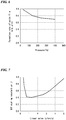
- FIG. 7 is a graph showing the relationship between the linear velocity and the BHF etching rate.
- the horizontal axis represents the linear velocity of the processing gas.
- the vertical axis represents the BHF etching rate, and the smaller the value, the higher the hydrofluoric acid resistance is. It can be understood from FIG. 7 that in the production method of this embodiment, the BHF etching rate takes a minimum value when the linear velocity is around 1.0 cm / sec, and the hydrofluoric acid resistance is the highest.
- FIG. 8 is a graph showing the relationship between a linear velocity and a formation rate of the oxide film.
- the horizontal axis represents the linear velocity of the processing gas.
- the vertical axis represents the formation rate of the oxide film, and the smaller the value, the higher the moisture resistance is. It can be understood from FIG. 8 that in the production method of this embodiment, the moisture resistance index takes a minimum value when the linear velocity is around 3.0 cm / sec, and the moisture resistance is the highest.
- the efficiency of generating active species in an appropriate dissociated state decrease, whether the linear velocity is too fast or too slow, so that a good quality film cannot be obtained. Therefore, in the production method of the present embodiment, it is preferable to adjust the linear velocity of the processing gas in a range of 0.3 to 5.0 cm/sec.
- the processing gas containing the organosilane gas and the hydrogen reducing gas supplied from the gas supply line L1 is excited by applying the electric power of a predetermined frequency to the showerhead gas introduction part 45 by the electric power source 46a.
- the frequency of the applied electric power is not particularly limited, but it can be appropriately selected from a frequency of 60 MHz or lower. As an example, at least part of the effects of the present embodiment can be achieved by using either one or both of 380 kHz and 13.56 MHz simultaneously, and continuously or intermittently.
- the electric power applied affects the dissociation state of the organosilane gas and the hydrogen reducing gas.
- FIG. 9 is a graph showing the relationship between a density of the high-frequency electric power and the BHF etching rate.
- the horizontal axis represents the density of the high-frequency electric power.
- the vertical axis shows the BHF etching rate, and the smaller the value, the higher the hydrofluoric acid resistance is. It can be understood from FIG. 9 that in the production method of this embodiment, the hydrofluoric acid resistance tends to be improved when the density of the high-frequency electric power is increased. On the other hand, decreasing the density of the high-frequency electric power tends to lower the hydrofluoric acid resistance.
- FIG. 10 is a graph showing the relationship between a density of the high-frequency electric power and a moisture resistance index.
- the horizontal axis represents the density of the high-frequency electric power.
- the vertical axis shows the formation rate of the oxide film, and the smaller the value, the higher the moisture resistance is. It can be understood from FIG. 10 that in the production method of the present embodiment, increasing the density of the high-frequency electric power tends to improve the moisture resistance. On the other hand, decreasing the density of the high-frequency electric power tends to lower the moisture resistance.
- the density of the high-frequency electric power is preferably 3.0 W/cm 2 or lower.
- the density of the high-frequency electric power is 0.4 W/cm 2 or more, the decomposition of the raw material is proceeded, and the formation rate is 1 nm/min or more, which is preferable from the viewpoint of productivity.
- the density of the high-frequency electric power is 0.2 W/cm 2 or lower, it is difficult to decompose the raw material and form SiN, which is not preferable from the viewpoint of productivity.
- the substrate When the density of the high-frequency electric power is 3.5 W/cm 2 , the substrate may be damaged depending on the device, and the device performance is deteriorated.
- the density of the high-frequency electric power within the range of 0.4 to 3.0 W/cm 2 .
- the density of the high-frequency electric power is a numerical value when the electrode area to be applied with high frequency is 452 cm 2 .
- the high-frequency electric power may be 90 W or more.
- the high-frequency electric power may be 1583 W or lower.
- the silicon nitride film 30 is produced on the substrate 20 by supplying the plasma generated to the substrate 20. Although gas is generated after the silicon nitride film 30 is produced, the vacuum pump 47 exhausts the gas generated to the outside of the process chamber 40 via the exhaust line L4.
- the silicon nitride film having the following film properties can be produced.
- the silicon nitride film obtained by the production method of the present embodiment described above that is, the silicon nitride film obtained by using the plasma CVD apparatus 100, and the organosilane gas as a raw material gas, adjusting the film formation temperature to 250°C or lower, using the processing gas obtained by adding the hydrogen reducing gas in a range of 200 to 2000 volumetric flow rate with respect to the organosilane gas of 1 volumetric flow rate, adjusting the pressure inside the process chamber 40 within the range of 35 to 400 Pa, and the density of the high-frequency electric power applied to the electrode installed in the process chamber 40 within the range of 0.2 to 3.5 W/cm 2 has the film properties shown in the following (a) to (c):
- the production method of the present embodiment is the plasma CVD method using the organosilane gas as a raw material gas, and adjusting the film formation temperature to 250°C or lower, wherein the processing gas obtained by adding a hydrogen reducing gas in a range of 200 to 2000 volumetric flow rate with respect to the organosilane gas of 1 volumetric flow rate is used, the pressure in the process chamber accommodating the substrate is adjusted to be in a range of 35 to 400 Pa, and the electric power density of high frequency applied to the showerhead gas introduction part 45 installed in the process chamber 40 is adjusted to be in a range of 0.2 to 3.5 W/cm 2 .
- the linear velocity of the processing gas introduced into the process chamber within the range of 0.3 to 5.0 cm/sec.
- the formation rate of the silicon oxide film of 2 nm/hour is equivalent to 0.2 g/m 2 /day in the general moisture permeability evaluation method.
- Examples 1 to 8 a silicon nitride film was produced on a silicon substrate controlled at 250°C or lower based on the production method for a silicon nitride film of the present invention.
- Tris(dimethylamino)silane (3DMAS) or tetrakis(dimethylamino)silane (4DMAS) was used as the organosilane gas, and hydrogen gas (H 2 ) was used as the hydrogen reducing gas.
- the frequency of the electric power applied was 380 kHz or 13.56 MHz.
- Table 1 below shows production conditions such as the ratio of the flow rate of the hydrogen reducing gas to the flow rate of the organosilane gas, the linear velocity, the pressure in the process chamber, the electric power density and the like in each example.
- a silicon nitride film was produced on a silicon substrate controlled at 200°C or 250°C by using silane gas under optimal conditions from the viewpoint of film properties.
- Comparative Example 3 a silicon nitride film was produced on a silicon substrate of which the temperature was controlled at 350°C by using a silane gas.
- a silicon nitride film was produced on a silicon substrate controlled at 200°C by using tris(dimethylamino)silane (3DMAS) as the organosilane gas and hydrogen gas (H 2 ) as the hydrogen reducing gas.
- 3DMAS tris(dimethylamino)silane
- H 2 hydrogen gas
- Example 1 250 3DMAS/H2 1200 0.9 133 13.56 MHz 0.8
- Example 2 200 3DMAS/H2 875 0.5 133 13.56 MHz 2.5
- Example 3 200 3DMAS/H2 1000 1.8 50 13.56 MHz 1.5
- Example 4 200 3DMAS/H2 420 1.2 80 380 kHz 0.6
- Example 5 200 3DMAS/H2 420 0.8 120 380 kHz 1
- Example 6 250 3DMAS/H2 565 0.5 133 13.56 MHz 2.5
- Example 7 250 3DMAS/H2 420 1.2 80 380 kHz 1
- Example 8 250 4DMAS/H2 420 2.7 35 13.56 MHz 1.4 Comparative Example 1 200 SiH4/H2 4 1
- FTIR Fastier transform infrared absorption spectrophotometer
- the moisture resistance of the silicon nitride film was evaluated by collecting information on the Si-O bond in the film before and after the pressure cooker test (PCT) by FT-IR.
- the direct result obtained is the moisture absorption amount of the film. It had been separately confirmed that moisture permeation could be prevented by a silicon nitride film having a film thickness of 1 nm in terms of SiO 2 film when the moisture absorption amount corresponds to 1 nm of SiO 2 film.
- the film with less moisture absorption means higher moisture barrier property.
- PCT conditions were 208 kPa and 121°C. This corresponds to an acceleration test of 10,000 times at the normal temperature and under the atmospheric pressure.
- the hydrofluoric acid resistance of the silicon nitride film was evaluated using a BHF (buffered hydrofluoric acid) solution. Specifically, the silicon nitride film was immersed in 16 BHF (20.8% NH 4 HF 2 -containing aqueous solution, produced by Morita Chemical Industry Co., Ltd.), after a predetermined time has elapsed, the silicon nitride film was quickly rinsed with pure water and dried with nitrogen gas or the like, and the BHF etching rate R was evaluated using the following equation (1).
- d 1 represents the film thickness before the immersion treatment
- d 2 represents the film thickness after the immersion treatment
- t represents the immersion time.
- the film thickness was measured by spectroscopic ellipsometry to be described later.
- R d 1 ⁇ d 2 / t
- the internal stress of the silicon nitride film was measured by a thin film stress measuring apparatus (FLX-2320-R, produced by Toho Technology Co., Ltd.) using the measuring principle based on the amount of warpage change of the substrate.
- the insulating property of the silicon nitride film was evaluated by mercury probe type IV measurement apparatus (SSM 495 produced by Solid State Measurement). Specifically, the insulating property was evaluated based on the leakage current value when the electric field intensity was 1 MV/cm.
- the refractive index and film thickness of the silicon nitride film were measured using spectroscopic ellipsometry (GES 5 E made by SOPRA).
- Table 2 shows the evaluation results of the film properties of the silicon nitride film produced in Examples 1 to 8 and Comparative Examples 1 to 3.
- the formation rate of silicon oxide during the silicon nitride film is exposed to the saturated water vapor atmosphere at 208 kPa and 121°C was 2 nm/hour in terms of a silicon oxide film in Examples 1 to 8. It is confirmed that the silicon nitride film of Examples 1 to 8 has the moisture resistance and the moisture barrier properties which are equal to or higher than those of the silicon nitride film of Comparative Examples 1 to 3.
- the leakage current value when applying 1 MV/cm electrolysis was 1.0 ⁇ 10 -6 A/cm 2 or lower and also had high insulating properties in Examples 1 to 6, and 8.
- Example 1 had an excellent insulation property of 7 ⁇ 10 -8 A/cm 2 or lower although it is not as good as Comparative Example using silane gas as the raw material gas.
- Comparative Example 4 when the flow rate ratio of the organosilane gas with respect to the hydrogen reducing gas under the production conditions of the silicon nitride film was set to 133, the formation rate of the silicon oxide during exposure to the saturated steam atmosphere at 208 kPa and 121°C was 2.3 nm/hour in terms of the silicon oxide film, and it is found that humidity resistance and moisture barrier property are deteriorated.
- Comparative Example 5 when the linear velocity under the production conditions of the silicon nitride film was set to 0.2 cm/sec, the formation rate of the silicon oxide during the exposure to the saturated water vapor atmosphere at 208 kPa and 121°C was 29.2 nm/hour in terms of a silicon oxide film, and it is found that the moisture resistance and moisture barrier property decrease.
- Example 1 1.8 8 1.9 -17 0.07
- Example 2 1.93 2.8 0.5 178 0.71
- Example 3 1.89 0.3 0.2 585 0.23
- Example 4 1.89 0.4 0.5 2 0.85
- Example 5 1.92 0.4 0.8 -188 0.92
- Example 6 1.92 2.2 0.6 109 0.83
- Example 7 1.93 0.2 1.2 -562 3.3
- Example 8 1.87 7.5 1.1 728 0.56 Comparative Example 1 1.91 161.7 1 -72 0.01 Comparative Example 2 1.94 67 0.5 -65 0.005 Comparative Example 3 2.04 12.9 0.5 -166 0.003 Comparative Example 4 1.91 0.6 2.3 135 0.52 Comparative Example 5 1.82 9.7 29.2 -30 0.9
- the method for producing a silicon nitride film of the present invention can be used as a method for producing a mask material in the production process of a semiconductor device such as an electronic device or an optical device, a metal diffusion preventing film, an oxidation barrier film, a passivation film, an insulating film, and so on.
Landscapes
- Chemical & Material Sciences (AREA)
- Engineering & Computer Science (AREA)
- Materials Engineering (AREA)
- General Chemical & Material Sciences (AREA)
- Chemical Kinetics & Catalysis (AREA)
- Mechanical Engineering (AREA)
- Metallurgy (AREA)
- Organic Chemistry (AREA)
- Inorganic Chemistry (AREA)
- Physics & Mathematics (AREA)
- Plasma & Fusion (AREA)
- Formation Of Insulating Films (AREA)
- Spectroscopy & Molecular Physics (AREA)
- Chemical Vapour Deposition (AREA)
Abstract
Description
- The present invention relates to a method for producing a silicon nitride film and a silicon nitride film.
- Since a silicon nitride film is excellent in chemical stability, the silicon nitride film has been used as a mask material in a producing process of a semiconductor device such as an electronic device and an optical device, a metal diffusion preventing film, an oxidation barrier film, a passivation film, an insulating film and the like in a semiconductor device.
- As a method for producing the silicon nitride film on a substrate, a thermal chemical vapor deposition method (thermal CVD method) in which a mixed gas of silane chloride and ammonia is supplied onto the substrate heated to 700°C or higher to form the silicon nitride film, a plasma chemical vapor deposition method (plasma CVD method) in which active species obtained by exciting a mixed gas of silane and ammonia with plasma are supplied onto the substrate heated to 350°C or higher to form the silicon nitride film, and the like have been widely used.
- In recent years, along with miniaturization and high integration of semiconductor devices and expansion of applications of the silicon nitride film itself, substrates and underlying layers for producing a silicon nitride film have diversified, and underlying layers having low thermal resistance are increasing. Therefore, it is desired to produce a silicon nitride film by a plasma CVD method at 300°C or lower, and preferably at 250°C or lower.
- In general, however, it is difficult to control the composition of atoms constituting the silicon nitride film and the bonding state between atoms when the film formation temperature is lowered. For this reason, it is well known that the film structure becomes coarse as compared with the case where the plasma CVD method is performed at a substrate temperature of more than 350 °C, and the bonding between silicon atoms and hydrogen atoms, and the bonding between nitrogen atoms and hydrogen atoms increase, chemical stability is decreased.
- On the other hand, when another thin film is formed on the silicon nitride film used for an insulating layer or the like, there is a possibility that contaminants such as organic substances, particles, and so on, may adhere to the surface of the silicon nitride layer. Therefore, prior to producing the thin film, a cleaning process may be performed to immerse the surface of the silicon nitride layer in a cleaning liquid such as diluted hydrofluoric acid to remove contaminants. For this process, when the silicon nitride film is scraped off in the cleaning process, the predetermined function cannot be exerted, so that a high hydrofluoric acid resistance is required for the silicon nitride film.
- Likewise, even when the silicon nitride film is used as an etching stopper layer in an etching process for producing a device, the silicon nitride film is required to have high hydrofluoric acid resistance. Therefore, if the chemical stability of the silicon nitride film is lowered due to the above-mentioned reasons, there is a possibility that the function as the metal diffusion preventing film, the oxidation barrier film, the passivation film, the insulating film and the like cannot be fulfilled.
- In response to such problems,
Patent Document 1 discloses a method for producing a silicon nitride film having a wet etching rate to a hydrofluoric acid solution (1% HF aqueous solution) of less than 50 nm/min by a high-density plasma CVD apparatus. However, the substrate temperature is about 450°C, which is insufficient for the above-mentioned requirement of 250°C or lower. This means that it is difficult to produce a silicon nitride film having high hydrofluoric acid resistance. - In addition,
Patent Document 2 discloses a plasma CVD method using an organosilazane compound as a method for producing a SiNCH film having a hydrofluoric acid resistance and a low leakage current value (high insulating property) at a substrate temperature of 200°C to 400°C. However, quantitative numerical values of hydrofluoric acid resistance and insulating properties are not disclosed. In addition, the moisture resistance required for the oxidation barrier film and the passivation film is not discussed. - Further,
Patent Document 3 discloses a plasma CVD method for producing a silicon nitride film effective for a passivation film at 200°C or lower. However, the film property being discussed is the gas permeability only, and the hydrofluoric acid resistance which is indispensable for producing the device is not discussed. - Meanwhile, in order to utilize the silicon nitride film as a thin film constituting a semiconductor device, it is also necessary to produce the silicon nitride film having a small internal stress for the purpose of preventing deformation of the substrate and film peeling.
Patent Document 4 discloses a method for producing a silicon nitride film, and examples in which the internal stress of the silicon nitride film produced in a range of 25°C to 250°C is in a range of -200 MPa to 200 MPa. However, there is no disclosure of film properties other than the internal stress. -
Patent Document 5 discloses a technique capable of controlling the film stress of the silicon nitride film formed on the substrate of 100°C or lower in a range of -400 to +100 MPa by controlling the hydrogen gas flow rate and the microwave output in the plasma CVD method using silane or disilane. However, there is no disclosure of the influence on the moisture resistance or the insulation at all. -
- Patent Document 1: Japanese Patent No.
5269093 - Patent Document 2: Japanese Patent No.
4048112 - Patent Document 3: Japanese Unexamined Patent Application, First Publication No.
2011-89186 - Patent Document 4: Japanese Unexamined Patent Application, First Publication No.
H09-186153 - Patent Document 5: Japanese Unexamined Patent Application, Publication No.
2012-188735 - Meanwhile, a recent demand for producing a silicon nitride film by a plasma CVD method is that a film, which has a wet etching rate lower and a moisture resistance equal to or higher than those of a conventional silicon nitride film produced at a substrate temperature of 350°C or higher, is formed on a substrate controlled to be at a temperature of 250°C or lower. At the same time, it is also demanded that the internal stress in the film is able to be arbitrarily controlled.
- However, there is a problem in lowering the substrate temperature in that it leads to deterioration of various properties such as high hydrofluoric acid resistance, high barrier properties, adjustment to an appropriate internal stress, high insulation and the like, which are required for a thin film constituting a semiconductor device or the like.
- As described above, improvement in film properties has been attempted by adjusting the film forming conditions. However, since the influence on each film property is different for each condition factor, there is no established method for producing a silicon nitride film having multiple improved film properties at the same time.
- The present invention has been made in view of the above circumstances, and it is an object of the present invention to provide a method for producing a silicon nitride film having a high hydrofluoric acid resistance, a high moisture resistance and an appropriate internal stress according to a demand of the device at a film formation temperature of 250°C or lower, and the silicon nitride film.
- Generally, it is known that when hydrogen atoms are present in a large amount in the silicon nitride film, that is, when there are many Si-H bonds or N-H bonds, for example, the hydrofluoric acid resistance and the moisture resistance deteriorate. Particularly, in the case of the plasma CVD method, a large amount of hydrogen atoms is liberated along with dissociation of interatomic bonds in the raw material gas and incorporated into the film, so that it is difficult to produce a film having high quality. As a countermeasure, it is known that the hydrofluoric acid resistance can be improved by using a carbon-containing raw material gas to add carbon atoms into the silicon nitride film. On the other hand, it is also known that the insulation deteriorates due to the above measures.
- The inventors of the present invention have conducted intensive studies to solve these conflicting problems and have reached the present invention. That is, the inventors of the present invention invented a method for simultaneously improving the hydrofluoric acid resistance and moisture resistance while suppressing the amount of carbon added to the silicon nitride film. Specifically, the inventors of the present invention have found that a method for achieving compatibility between a technique of exhausting either or both excessive carbon atoms and hydrogen atoms in the plasma space as they are, and a technique of incorporating an appropriate amount of carbon atoms with a low conductivity coupled state into a film by appropriately adjusting a plurality of silicon nitride film producing condition factors.
- Although the structure itself of the silicon nitride film has not been elucidated, the present inventors have found that a silicon nitride film, which has a wet etching rate lower and a moisture resistance equal to or higher than those of a conventional silicon nitride film produced at a substrate temperature of 350°C or higher and an appropriate internal stress, can be obtained by the method above. Specifically, the inventors of the present invention have found that according to the above method, a silicon nitride film in which (a) an etching rate by a hydrofluoric acid solution is 10 nm/min or lower, (b) a formation rate of a silicon oxide while being exposed to a saturated water vapor atmosphere at 208 kPa and 121°C is 2 nm/hour or lower in terms of a silicon oxide film, and (c) an internal stress in the film is in the range of -1000 to 1000 MPa can be obtained by the method above.
- In other words, the present invention provides the following methods for producing a silicon nitride film and silicon nitride films according to (1) to (8).
- (1) A method for producing a silicon nitride film having the following film properties (a) to (c) on a substrate having a temperature of 250°C or lower by using an organosilane gas as a raw material gas by a plasma chemical vapor deposition method, wherein a processing gas obtained by adding a hydrogen reducing gas in a range of 200 to 2000 volumetric flow rate to an organosilane gas of 1 volumetric flow rate is used, a pressure in a process chamber accommodating the substrate is adjusted to be in a range of 35 to 400 Pa, and a density of high-frequency electric power applied to an electrode installed in the process chamber is adjusted to be in a range of 0.2 to 3.5 W/cm2,
- (a) an etching rate by a hydrofluoric acid solution is 10 nm/min or lower,
- (b) a formation rate of a silicon oxide while being exposed to a saturated water vapor atmosphere at 208 kPa and 121°C is 2 nm/hour or lower in terms of a silicon oxide film, and
- (c) an internal stress in the film is in the range of -1000 to 1000 MPa.
In the production method above, it is preferable to adjust a linear velocity of the processing gas introduced into the process chamber to be in a range of 0.3 to 5.0 cm/sec.
The above "linear velocity" means a value calculated by:
total flow rate of supply gas / plasma generation area × (atmospheric pressure / processing pressure).
In addition, "plasma generation area" above means an area of an electrode for plasma generation.
- (2) The method for producing a silicon nitride film according to (1), wherein a linear velocity of the processing gas introduced into the process chamber is adjusted to be in a range of 0.3 to 5.0 cm/sec.
- (3) The method for producing a silicon nitride film according to (1) or (2), wherein the organosilane gas is represented by a formula (R1R2N)nSiH4-n (wherein R1 and R2 are each independently a hydrocarbon group and n is any one of 2, 3 and 4).
- (4) The method for producing a silicon nitride film according to (3), wherein the hydrocarbon group is a methyl group or an ethyl group.
- (5) The method for producing a silicon nitride film according to (1), wherein the organosilane gas contains at least one selected from the group consisting of tetrakis(dimethylamino)silane, tris(dimethylamino)silane, bis(dimethylamino)silane, tetrakis(diethylamino)silane, tris(diethylamino)silane, bis(diethylamino)silane, tetrakis(ethylmethylamino)silane, tris(ethylmethylamino)silane, and bis(ethylmethylamino)silane.
- (6) The method for producing a silicon nitride film according to any one of (1) to (5), wherein the hydrogen reducing gas includes a hydrogen atom.
- (7) The method for producing a silicon nitride film according to (6), wherein the hydrogen reducing gas contains at least one selected from the group consisting of ammonia, amine, and hydrocarbon.
- (8) A silicon nitride film having following film properties (a) to (c) which is produced by a plasma chemical vapor deposition method, wherein an organosilane gas is used as a raw material gas, a film formation temperature is adjusted to 250°C or lower, a processing gas obtained by adding a hydrogen reducing gas in a range of 200 to 2000 volumetric flow rate with respect to the organosilane gas of 1 volumetric flow rate is used, a pressure in a process chamber accommodating a substrate is adjusted to be in a range of 35 to 400 Pa, and a density of high-frequency electric power applied to an electrode installed in the process chamber is adjusted to be in a range of 0.2 to 3.5 W/cm2,
- (a) an etching rate by a hydrofluoric acid solution is 10 nm/min or lower,
- (b) a formation rate of a silicon oxide while being exposed to a saturated water vapor atmosphere at 208 kPa and 121°C is 2 nm/hour or lower in terms of a silicon oxide film, and
- (c) an internal stress in the film is in a range of -1000 to 1000 MPa.
- In the method for producing a silicon nitride film according to the present invention, when the silicon nitride film is produced by a plasma chemical vapor deposition method using an organosilane gas as a raw material gas and adjusting a film formation temperature to 250°C or lower, a processing gas obtained by adding a hydrogen reducing gas in a range of 200 to 2000 volumetric flow rate with respect to the organosilane gas of 1 volumetric flow rate is used, the pressure in a process chamber accommodating a substrate is adjusted to be in a range of 35 to 400 Pa, and the density of high-frequency electric power applied to an electrode installed in the process chamber is adjusted to be in a range of 0.2 to 3.5 W/cm2.
- As a result, it is possible to produce a silicon nitride film having a high hydrofluoric acid resistance, a high moisture resistance and an appropriate internal stress according to the demands of the device side.
- The silicon nitride film according to the present invention is a film which is produced by a plasma chemical vapor deposition method, wherein an organosilane gas is used as a raw material gas, a film formation temperature is adjusted to 250°C or lower, a processing gas obtained by adding a hydrogen reducing gas in a range of 200 to 2000 volumetric flow rate with respect to the organosilane gas of 1 volumetric flow rate is used, the pressure in a process chamber accommodating a substrate is adjusted to be in a range of 35 to 400 Pa, and the density of high-frequency electric power applied to an electrode installed in the process chamber is adjusted to be in a range of 0.2 to 3.5 W/cm2.
- As a result, the silicon nitride film has a high hydrofluoric acid resistance, a high moisture resistance and an appropriate internal stress according to the demands of the device side.
-
-
FIG.1 is a diagram showing an example of a plasma CVD apparatus used in a method for producing a silicon nitride film which is one embodiment according to the present invention. -
FIG. 2 is a graph showing a relationship between a gas ratio and a BHF etching rate. -
FIG. 3 is a graph showing a relationship between a gas ratio and a formation rate of an oxide film. -
FIG. 4 is a graph showing a relationship between a gas ratio and a formation rate of a silicon nitride film. -
FIG. 5 is a graph showing a relationship between a pressure and a BHF etching rate. -
FIG. 6 is a graph showing a relationship between a pressure and a formation rate of an oxide film. -
FIG. 7 is a graph showing a relationship between a linear velocity and a BHF etching rate. -
FIG. 8 is a graph showing a relationship between a linear velocity and a formation rate of an oxide film. -
FIG. 9 is a graph showing a relationship between a density of high-frequency electric power and a BHF etching rate. -
FIG. 10 is a graph showing a relationship between a density of high-frequency electric power and a formation rate of an oxide film. - Hereinafter, one embodiment of the method for producing a silicon nitride film according to the present invention will be described in detail with reference to the drawings. In the drawings used in the following description, in order to make the features easy to understand, there are cases where characteristic portions are enlarged for the sake of convenience, and the dimensional ratios and the like of each component are not always the same as the actual ones.
- First, the configuration of an apparatus for producing a silicon nitride film which can be used in one embodiment of the method for producing a silicon nitride film according to the present invention will be described. That is, an example of a configuration of a plasma chemical vapor deposition apparatus (plasma CVD apparatus) used in the method for producing a silicon nitride film according to this embodiment will be described.
-
FIG. 1 is a diagram showing an example of a plasma CVD apparatus used in a method for producing a silicon nitride film which is one embodiment of the present invention. - As shown in
FIG. 1 , aplasma CVD apparatus 100 mainly includes asubstrate 20, aprocess chamber 40, astage 41,heaters gas introduction part 45,electric power sources vacuum pump 47, an exhaustflow rate regulator 48, acontrol unit 49, an organosilanegas supply source 50, a first hydrogen reducinggas supply source 52, a second hydrogen reducinggas supply source 54, gasflow rate regulators computer 60, and an insulation part S. - The
substrate 20 is provided on thestage 41, and asilicon nitride film 30 is produced on thesubstrate 20. The material of thesubstrate 20 is not particularly limited as long as it has heat resistance at a film formation temperature of 250°C. Specifically, for example, quartz or the like can be used. - The
process chamber 40 accommodates thesubstrate 20, and includes thestage 41, theheaters gas introduction part 45. An organosilane gas is supplied from the organosilanegas supply source 50 into theprocess chamber 40, and hydrogen reducing gas is supplied from the first hydrogen reducinggas supply source 52 and the second hydrogen reducinggas supply source 54 into theprocess chamber 40 to produce thesilicon nitride film 30. - The
stage 41 is provided near the center of theprocess chamber 40. - The
heater 44a is provided on the upper portion of the showerheadgas introduction portion 45 and the side surface of theprocess chamber 40, and theheater 44b is provided on the underside of thestage 41 so that the temperature in theprocess chamber 40 and thesubstrate 20 can be adjusted. The upper limit of the substrate temperature is not particularly limited, but preferably 250 °C or lower from the background of the demand for low temperature film formation. - The showerhead
gas introduction part 45 is provided upper portion of theprocess chamber 40. The organosilane gas and the hydrogen reducing gas are introduced into theprocess chamber 40 via the showerheadgas introduction part 45. - The
electric power source 46a is connected to the showerheadgas introduction part 45 via the electric power supply wire P1. On the other hand, theelectric power source 46b is connected to thestage 41 via the electric power supply wire P2. By applying electric power with a predetermined frequency to the showerheadgas introduction part 45 from theelectric power source 46a, a mixed gas of organosilane gas and a hydrogen reducing gas which are discharged from the showerheadgas introduction part 45 can be converted into plasma. Electric power with a predetermined frequency is applied to thestage 41 from theelectric power source 46b as necessary, and the generated plasma is supplied to thesubstrate 20 on thestage 41. Thesilicon nitride film 30 is produced on thesubstrate 20 exposed to the plasma. Theelectric power sources - The
vacuum pump 47 is connected to theprocess chamber 40 via an exhaust line L4. Thevacuum pump 47 can reduce the pressure in theprocess chamber 40 and exhaust the gas generated after thesilicon nitride film 30 is produced. - The exhaust
flow rate regulator 48 is provided in the exhaust line L4, and can adjust the exhaust flow rate of the gas exhausted by thevacuum pump 47. The exhaustflow rate regulator 48 is not particularly limited, but it may be controlled manually or automatically by an external control device. - The
control unit 49 is connected to theheater 44a via the signal line C1, theheater 44b via the signal line C2, theelectric power source 46a via the signal line C3, theelectric power source 46b via the signal line C4, the gasflow rate regulator 51 via the signal line C5, the gasflow rate regulator 53 via the signal line C6, the gasflow rate regulator 55 via the signal line C7, and the exhaustflow rate regulator 48 via the signal line C8. Thecontrol unit 49 can control theheaters electric power sources flow rate regulators flow rate regulator 48. Thecontrol unit 49 is connected to thecomputer 60. - The organosilane
gas supply source 50 is connected to the showerheadgas introduction part 45 provided in theprocess chamber 40 via the gas supply line L1, and can supply the organosilane gas into theprocess chamber 40. The organosilanegas supply source 50 is not particularly limited. Specifically, for example, a cylinder filled with an organosilane gas or the like can be used. - In addition, the organosilane gas is not particularly limited, but examples thereof include tetrakis(dimethylamino)silane, tris(dimethylamino)silane, bis(dimethylamino)silane, tetrakis(diethylamino)silane, tris(diethylamino)silane, bis(diethylamino)silane, tetrakis(ethylmethylamino)silane, tris(ethylmethylamino)silane, bis(ethylmethylamino)silane, and the like.
- The first hydrogen reducing
gas supply source 52 is connected to the showerheadgas introduction unit 45 provided in theprocess chamber 40 via a first hydrogen reducing gas supply line L2 and a gas supply line L1, and supplies hydrogen reducing gas into theprocess chamber 40. The first hydrogen reducinggas supply source 52 is not particularly limited, but specifically, for example, a cylinder filled with the hydrogen reducing gas supply source or the like can be used. - In addition, the hydrogen reducing gas is not particularly limited, but specifically, for example, hydrogen gas (H2), ammonia gas (NH3), amines, hydrocarbons and the like can be used.
- The second hydrogen reducing
gas supply source 54 is connected to the showerheadgas introduction part 45 provided in theprocess chamber 40 via a second hydrogen reducing gas supply line L3 and a gas supply line L1, and supplies hydrogen reducing gas into theprocess chamber 40. A mixture of two kinds of hydrogen reducing gases can be used by using the second hydrogen reducinggas supply source 54 in addition to the first hydrogen reducinggas supply source 52. The second hydrogen reducinggas supply source 54 is not particularly limited, but specifically, for example, a cylinder filled with a hydrogen reducing gas supply source or the like can be used. - The gas
flow rate regulator 51 is provided on the primary side of the gas supply line L1 to a junction with the first hydrogen reducing gas supply line L2 and regulates the flow rate of the organosilane gas supplied from the organosilanegas supply source 50. Further, the gasflow rate regulator 53 is provided in the first hydrogen reducing gas supply line L2, and can adjust the flow rate of the hydrogen reducing gas supplied from the first hydrogen reducinggas supply source 52. Further, the gasflow rate regulator 55 is provided in the second hydrogen reducing gas supply line L3, and can regulate the flow rate of the hydrogen reducing gas supplied from the second hydrogen reducinggas supply source 54. The gasflow rate regulators - The insulating portion S is provided between the showerhead
gas introduction part 45 and theprocess chamber 40, and can electrically insulate between the showerheadgas introduction part 45 and theprocess chamber 40. Further, the insulating portion S is also provided between thestage 41 and theprocess chamber 40, so that thestage 41 and theprocess chamber 40 can be electrically insulated. - Next, a method for producing a silicon nitride film of the present embodiment (hereinafter simply referred to as "production method") using the above-described
plasma CVD apparatus 100 will be described. - The production method according to this embodiment is a method for producing a silicon nitride film having desired film properties by a plasma chemical vapor deposition method (Plasma CVD method) including an introduction step of introducing a processing gas into the
process chamber 40 accommodating thesubstrate 20 under a predetermined gas introduction condition, a plasma exciting step of plasma exciting the processing gas by applying high-frequency electric power, and a silicon nitride forming step of forming asilicon nitride film 30 on thesubstrate 20 using plasma active species. - Specifically, the production method according to this embodiment is the plasma CVD method above, wherein an organosilane gas is used as a raw material gas, a film formation temperature is adjusted to 250°C or lower, a processing gas obtained by adding a hydrogen reducing gas in a range of 200 to 2000 volumetric flow rate with respect to the organosilane gas of 1 volumetric flow rate is used, the pressure in the
process chamber 40 is adjusted to be in a range of 35 to 400 Pa, and the density of high-frequency electric power applied to the showerheadgas introduction part 45 installed in theprocess chamber 40 is adjusted to be in a range of 0.2 to 3.5 W/cm2. - The film properties evaluation methods will be described later.
- Hereinafter, the production method of the present embodiment will be described in detail.
- First, the
substrate 20 is placed on thestage 41, and heated by theheater 44b until thesubstrate 20 reaches a predetermined temperature. The upper limit of the substrate temperature is not particularly limited, but it is preferable to set it at 250°C or lower from the background of the demand for low temperature film formation. - Next, the organosilane gas supplied from the organosilane
gas supply source 50 is diluted with a large amount of the hydrogen reducing gas supplied from the first hydrogen reducinggas supply source 52 and the second hydrogen reducinggas supply source 54, and then the gas diluted is supplied into theprocess chamber 40 via the supply line L1. By performing the dilution operation described above, in addition to the effect of reducing the amount of carbon atoms and hydrogen atoms incorporated into the film, an effect of not forming a C=C bond with low binding energy in the film is obtained. - Here, the results of examination by the present inventors on the relationship between the gas ratio of the hydrogen reducing gas with respect to the organosilane gas of 1 volumetric flow rate and the film properties are shown in
FIGS. 2 to 4 , respectively. -
FIG. 2 is a graph showing the relationship between a gas ratio and a BHF etching rate. InFIG. 2 , the horizontal axis represents the gas ratio of the hydrogen reducing gas with respect to the organosilane gas of 1 volumetric flow rate. On the other hand, the vertical axis represents the BHF etching rate, and the smaller the value, the higher the hydrofluoric acid resistance is. - It can be understood from
FIG. 2 that in the production method of the present embodiment, increasing the gas ratio tends to improve hydrofluoric acid resistance. On the other hand, when the gas ratio is decreased, the hydrofluoric acid resistance tends to decrease. -
FIG. 3 is a graph showing the relationship between a gas ratio and a formation rate of the oxide film. InFIG. 3 , the horizontal axis represents the gas ratio of the hydrogen reducing gas with respect to the organosilane gas of 1 volumetric flow rate. On the other hand, the vertical axis represents the formation rate of the oxide film, and the smaller the value, the higher the moisture resistance is. Moreover, it should be noted that in the silicon nitride film of the present invention, generation of an oxide film proceeds from the surface side of the silicon nitride film, and moisture does not permeate to a depth deeper than the thickness of the generated oxide film has been confirmed separately by experiments. It can be understood fromFIG. 3 that in the production method of this embodiment, increasing the gas ratio tends to improve moisture resistance. On the other hand, when the gas ratio is decreased, humidity resistance tends to decrease. -
FIG. 4 is a graph showing the relationship between a gas ratio and a formation rate of the silicon nitride film. InFIG. 4 , the horizontal axis represents the gas ratio of the hydrogen reducing gas with respect to the organosilane gas of 1 volumetric flow rate. On the other hand, the vertical axis represents the formation rate of the silicon nitride film, and the larger the value, the faster the formation rate of the silicon nitride film. It can be understood fromFIG. 4 that in the production method of this embodiment, increasing the gas ratio tends to decrease the deposition rate of the silicon nitride film. On the other hand, when the gas ratio is decreased, the formation rate of the silicon nitride film tends to increase. - As a result of the above investigations, as the gas ratio of the hydrogen reducing gas with respect to the organosilane gas of 1 volumetric flow rate is increased, the hydrofluoric acid resistance and the moisture resistance are improved, whereas the formation rate decreases and the productivity decreases. Therefore, in the production method of this embodiment, it is preferable to use a processing gas to which hydrogen reducing gas in a range of 200 to 2000 volumetric flow rate is added to the organosilane gas of 1 volumetric flow rate.
- The adjustment of the gas ratio is performed by adjusting the flow rate of each gas. Specifically, the flow rate of the organosilane gas is adjusted by the gas
flow rate regulator 51, the flow rate of the hydrogen reducing gas supplied from the first hydrogen reducinggas supply source 52 is adjusted by the gasflow rate regulator 53, and the flow rate of the hydrogen reducing gas supplied from the second hydrogen reducinggas supply source 54 is adjusted by the gasflow rate regulator 55. - On the other hand, the internal pressure in the
process chamber 40 to which the processing gas is supplied is controlled by thevacuum pump 47. The pressure in theprocess chamber 40 affects the residence time of the raw material gas in theprocess chamber 40 from the decomposition of the raw material gas in the plasma to the reaction on thesubstrate 20, the plasma discharge state, and the collision frequency. As a result, the pressure in theprocess chamber 40 also affects the film properties of the silicon nitride film to be produced. Specifically, as the pressure is lowered, the collision frequency decreases and the dissociation becomes insufficient. When the pressure is further lowered, the plasma state becomes unstable. On the other hand, as the pressure is increased, the mean free path becomes shorter and sufficient acceleration energy cannot be obtained, and further raising makes it difficult to maintain the plasma state. - Here, the results of examination by the present inventors on the relationship between the pressure in the
process chamber 40 and the film properties are shown inFIGS. 5 and6 , respectively. -
FIG. 5 is a graph showing the relationship between the pressure and the BHF etching rate. InFIG. 5 , the horizontal axis represents the pressure in theprocess chamber 40. On the other hand, the vertical axis represents the BHF etching rate, and the smaller the value, the higher the hydrofluoric acid resistance is. It can be understood fromFIG 5 that in the production method of this embodiment, increasing the pressure in theprocess chamber 40 tends to lower the hydrofluoric acid resistance. On the other hand, decreasing the pressure in theprocess chamber 40 tends to improve hydrofluoric acid tolerance. -
FIG. 6 is a graph showing the relationship between a pressure and a formation rate of the oxide film. InFIG. 6 , the horizontal axis represents the pressure in theprocess chamber 40. On the other hand, the vertical axis represents the formation rate of the oxide film, and the smaller the value, the higher the moisture resistance is. It can be understood fromFIG. 6 that in the production method of the present embodiment, increasing the pressure in theprocess chamber 40 tends to improve the moisture resistance. On the other hand, when the pressure in theprocess chamber 40 is decreased, the moisture resistance tends to decrease. - From the results above, it can be understood that as the pressure in the
process chamber 40 is increased, the moisture resistance improves, but on the other hand, the hydrofluoric acid resistance decreases. Therefore, in the production method of the present embodiment, it is preferable to adjust the pressure inside theprocess chamber 40 to be in a range of 35 to 400 Pa. - Further, the linear velocity of the processing gas supplied into the
process chamber 40 is controlled by the gasflow rate regulators process chamber 40. Like the pressure in theprocess chamber 40, the linear velocity of the processing gas also affects the residence time of the raw material gas in theprocess chamber 40 from the decomposition of the raw material gas in the plasma to the reaction on thesubstrate 20, the state of plasma discharge and the frequency of collisions. - Here, the results of examination by the present inventors on the relationship between the linear velocity of the processing gas and the film properties are shown in
FIGS. 7 and8 , respectively. -
FIG. 7 is a graph showing the relationship between the linear velocity and the BHF etching rate. InFIG. 7 , the horizontal axis represents the linear velocity of the processing gas. On the other hand, the vertical axis represents the BHF etching rate, and the smaller the value, the higher the hydrofluoric acid resistance is. It can be understood fromFIG. 7 that in the production method of this embodiment, the BHF etching rate takes a minimum value when the linear velocity is around 1.0 cm / sec, and the hydrofluoric acid resistance is the highest. -
FIG. 8 is a graph showing the relationship between a linear velocity and a formation rate of the oxide film. InFIG. 8 , the horizontal axis represents the linear velocity of the processing gas. On the other hand, the vertical axis represents the formation rate of the oxide film, and the smaller the value, the higher the moisture resistance is. It can be understood fromFIG. 8 that in the production method of this embodiment, the moisture resistance index takes a minimum value when the linear velocity is around 3.0 cm / sec, and the moisture resistance is the highest. - From the results above, it can be understood that the efficiency of generating active species in an appropriate dissociated state decrease, whether the linear velocity is too fast or too slow, so that a good quality film cannot be obtained. Therefore, in the production method of the present embodiment, it is preferable to adjust the linear velocity of the processing gas in a range of 0.3 to 5.0 cm/sec.
- Next, the processing gas containing the organosilane gas and the hydrogen reducing gas supplied from the gas supply line L1 is excited by applying the electric power of a predetermined frequency to the showerhead
gas introduction part 45 by theelectric power source 46a. - In the production method of the present embodiment, the frequency of the applied electric power is not particularly limited, but it can be appropriately selected from a frequency of 60 MHz or lower. As an example, at least part of the effects of the present embodiment can be achieved by using either one or both of 380 kHz and 13.56 MHz simultaneously, and continuously or intermittently. The electric power applied affects the dissociation state of the organosilane gas and the hydrogen reducing gas.
- Here, the results of examination by the present inventors on the relationship between the density of the high-frequency electric power and the film properties are shown in
FIG. 9 andFIG. 10 respectively. -
FIG. 9 is a graph showing the relationship between a density of the high-frequency electric power and the BHF etching rate. InFIG. 9 , the horizontal axis represents the density of the high-frequency electric power. On the other hand, the vertical axis shows the BHF etching rate, and the smaller the value, the higher the hydrofluoric acid resistance is. It can be understood fromFIG. 9 that in the production method of this embodiment, the hydrofluoric acid resistance tends to be improved when the density of the high-frequency electric power is increased. On the other hand, decreasing the density of the high-frequency electric power tends to lower the hydrofluoric acid resistance. -
FIG. 10 is a graph showing the relationship between a density of the high-frequency electric power and a moisture resistance index. InFIG. 10 , the horizontal axis represents the density of the high-frequency electric power. On the other hand, the vertical axis shows the formation rate of the oxide film, and the smaller the value, the higher the moisture resistance is. It can be understood fromFIG. 10 that in the production method of the present embodiment, increasing the density of the high-frequency electric power tends to improve the moisture resistance. On the other hand, decreasing the density of the high-frequency electric power tends to lower the moisture resistance. - From the results above, it can be understood that as the density of the high-frequency electric power increases, the hydrofluoric acid resistance and moisture resistance are improved. However, on the other hand, in order to avoid inconveniences such as high-frequency electric power source initial investment, power consumption cost and durability of the members constituting the plasma generating device, the density of the high-frequency electric power is preferably 3.0 W/cm2 or lower.
- In addition, when the density of the high-frequency electric power is 0.4 W/cm2 or more, the decomposition of the raw material is proceeded, and the formation rate is 1 nm/min or more, which is preferable from the viewpoint of productivity. When the density of the high-frequency electric power is 0.2 W/cm2 or lower, it is difficult to decompose the raw material and form SiN, which is not preferable from the viewpoint of productivity.
- When the density of the high-frequency electric power is 3.5 W/cm2, the substrate may be damaged depending on the device, and the device performance is deteriorated.
- Therefore, in consideration of the above effect and inconvenience, in the production method for a silicon nitride film of the present invention, it is preferable to adjust the density of the high-frequency electric power within the range of 0.4 to 3.0 W/cm2.
- Moreover, the density of the high-frequency electric power is a numerical value when the electrode area to be applied with high frequency is 452 cm2. In order to make the density of the high-frequency electric power be 0.2 W/cm2 or more, the high-frequency electric power may be 90 W or more. In order to make the density of the high-frequency electric power be 3.5 W/cm2 or lower, the high-frequency electric power may be 1583 W or lower.
- Finally, the
silicon nitride film 30 is produced on thesubstrate 20 by supplying the plasma generated to thesubstrate 20. Although gas is generated after thesilicon nitride film 30 is produced, thevacuum pump 47 exhausts the gas generated to the outside of theprocess chamber 40 via the exhaust line L4. - In this manner, the silicon nitride film having the following film properties can be produced.
- The silicon nitride film obtained by the production method of the present embodiment described above, that is, the silicon nitride film obtained by using the
plasma CVD apparatus 100, and the organosilane gas as a raw material gas, adjusting the film formation temperature to 250°C or lower, using the processing gas obtained by adding the hydrogen reducing gas in a range of 200 to 2000 volumetric flow rate with respect to the organosilane gas of 1 volumetric flow rate, adjusting the pressure inside theprocess chamber 40 within the range of 35 to 400 Pa, and the density of the high-frequency electric power applied to the electrode installed in theprocess chamber 40 within the range of 0.2 to 3.5 W/cm2 has the film properties shown in the following (a) to (c): - (a) an etching rate by a hydrofluoric acid solution is 10 nm/min or lower;
- (b) a formation rate of a silicon oxide while being exposed to a saturated water vapor atmosphere at 208 kPa and 121°C is 2 nm/hour or lower in terms of a silicon oxide film; and
- (c) an internal stress in the film is in the range of -1000 to 1000 MPa.
- As explained above, the production method of the present embodiment is the plasma CVD method using the organosilane gas as a raw material gas, and adjusting the film formation temperature to 250°C or lower, wherein the processing gas obtained by adding a hydrogen reducing gas in a range of 200 to 2000 volumetric flow rate with respect to the organosilane gas of 1 volumetric flow rate is used, the pressure in the process chamber accommodating the substrate is adjusted to be in a range of 35 to 400 Pa, and the electric power density of high frequency applied to the showerhead
gas introduction part 45 installed in theprocess chamber 40 is adjusted to be in a range of 0.2 to 3.5 W/cm2. - As a result, it is possible to produce a silicon nitride film having a high hydrofluoric acid resistance, a high moisture resistance and an appropriate internal stress (i.e., the film properties of the above (a) to (c)) according to the demands of the device side.
- Moreover, according to the production method of this embodiment, it is preferable to adjust the linear velocity of the processing gas introduced into the process chamber within the range of 0.3 to 5.0 cm/sec.
- In the following PCT results, the formation rate of the silicon oxide film of 2 nm/hour is equivalent to 0.2 g/m2/day in the general moisture permeability evaluation method.
- It should be noted that the technical scope of the present invention is not limited to the above embodiments, and various modifications can be made without departing from the spirit of the present invention. For example, although two types of hydrogen reducing gases are used by using the first hydrogen reducing
gas supply source 52 and the second hydrogen reducinggas supply source 54 in the production method of the embodiment above, one hydrogen reducing gas supply source may be provided. - In Examples 1 to 8, a silicon nitride film was produced on a silicon substrate controlled at 250°C or lower based on the production method for a silicon nitride film of the present invention.
- Tris(dimethylamino)silane (3DMAS) or tetrakis(dimethylamino)silane (4DMAS) was used as the organosilane gas, and hydrogen gas (H2) was used as the hydrogen reducing gas.
- The frequency of the electric power applied was 380 kHz or 13.56 MHz.
- Table 1 below shows production conditions such as the ratio of the flow rate of the hydrogen reducing gas to the flow rate of the organosilane gas, the linear velocity, the pressure in the process chamber, the electric power density and the like in each example.
- In Comparative Examples 1 and 2, a silicon nitride film was produced on a silicon substrate controlled at 200°C or 250°C by using silane gas under optimal conditions from the viewpoint of film properties.
- The production conditions of Comparative Examples 1 and 2 are shown in Table 1 below.
- In Comparative Example 3, a silicon nitride film was produced on a silicon substrate of which the temperature was controlled at 350°C by using a silane gas.
- The producing conditions of Comparative Example 3 are shown in Table 1 below.
- In Comparative Examples 4 and 5, a silicon nitride film was produced on a silicon substrate controlled at 200°C by using tris(dimethylamino)silane (3DMAS) as the organosilane gas and hydrogen gas (H2) as the hydrogen reducing gas.
Table 1 Temperature Gas Species Rate of Flow Rate Linear Velocity Pressure inside Process Chamber Frequency of Electric Power Applied Density of Electric Power Applied [°C] (Organosilane (1) / hydrogen reducing gas (2)) ((2)/(1)) [cm/sec.] [Pa] [W/cm2] Example 1 250 3DMAS/H2 1200 0.9 133 13.56 MHz 0.8 Example 2 200 3DMAS/H2 875 0.5 133 13.56 MHz 2.5 Example 3 200 3DMAS/ H2 1000 1.8 50 13.56 MHz 1.5 Example 4 200 3DMAS/H2 420 1.2 80 380 kHz 0.6 Example 5 200 3DMAS/H2 420 0.8 120 380 kHz 1 Example 6 250 3DMAS/H2 565 0.5 133 13.56 MHz 2.5 Example 7 250 3DMAS/H2 420 1.2 80 380 kHz 1 Example 8 250 4DMAS/H2 420 2.7 35 13.56 MHz 1.4 Comparative Example 1 200 SiH4/ H2 4 1 200 13.56 MHz 1.2 Comparative Example 2 250 SiH4/ H2 4 1 200 13.56 MHz 1.2 Comparative Example 3 350 SiH4/NH3 8 0.054 346 13.56MHz/ 250kHz 0.6 Comparative Example 4 200 3DMAS/H2 133 0.4 93 13.56MHz 1.9 Comparative Example 5 200 3DMAS/ H2 400 0.2 200 13.56MHz 1.7 - Film properties of the silicon nitride film produced were evaluated under the above conditions. Each evaluation method will be described below.
- The interatomic bonding state of the silicon nitride film was evaluated by measuring infrared absorption spectrum using FTIR (Fourier transform infrared absorption spectrophotometer,
spectrum 400 produced by Perkinelmer). Specifically, information such as Si-N bond, Si-H bond, N-H bond, C=N bond, C=C bond, Si-O bond, and so on, were collected and analyzed. - The moisture resistance of the silicon nitride film was evaluated by collecting information on the Si-O bond in the film before and after the pressure cooker test (PCT) by FT-IR. The direct result obtained is the moisture absorption amount of the film. It had been separately confirmed that moisture permeation could be prevented by a silicon nitride film having a film thickness of 1 nm in terms of SiO2 film when the moisture absorption amount corresponds to 1 nm of SiO2 film. The film with less moisture absorption means higher moisture barrier property.
- Moreover, the PCT conditions were 208 kPa and 121°C. This corresponds to an acceleration test of 10,000 times at the normal temperature and under the atmospheric pressure.
- The hydrofluoric acid resistance of the silicon nitride film was evaluated using a BHF (buffered hydrofluoric acid) solution. Specifically, the silicon nitride film was immersed in 16 BHF (20.8% NH4HF2-containing aqueous solution, produced by Morita Chemical Industry Co., Ltd.), after a predetermined time has elapsed, the silicon nitride film was quickly rinsed with pure water and dried with nitrogen gas or the like, and the BHF etching rate R was evaluated using the following equation (1).
- In the following formula (1), d1 represents the film thickness before the immersion treatment, d2 represents the film thickness after the immersion treatment, and t represents the immersion time. The film thickness was measured by spectroscopic ellipsometry to be described later.

- The internal stress of the silicon nitride film was measured by a thin film stress measuring apparatus (FLX-2320-R, produced by Toho Technology Co., Ltd.) using the measuring principle based on the amount of warpage change of the substrate.
- The insulating property of the silicon nitride film was evaluated by mercury probe type IV measurement apparatus (SSM 495 produced by Solid State Measurement). Specifically, the insulating property was evaluated based on the leakage current value when the electric field intensity was 1 MV/cm.
- The refractive index and film thickness of the silicon nitride film were measured using spectroscopic ellipsometry (GES 5 E made by SOPRA).
- The following Table 2 shows the evaluation results of the film properties of the silicon nitride film produced in Examples 1 to 8 and Comparative Examples 1 to 3.
- In all of Examples 1 to 8, it is found that the etching rate by the hydrofluoric acid solution is 10 nm/min or lower, and the silicon nitride film of Examples 1 to 8 has higher hydrofluoric acid resistance than that of the silicon nitride film of Comparative Example 3. Further, as shown in Comparative Examples 1 and 2, it is found that sufficient hydrofluoric acid resistance cannot be obtained by using the silane gas.
- Similarly, the formation rate of silicon oxide during the silicon nitride film is exposed to the saturated water vapor atmosphere at 208 kPa and 121°C was 2 nm/hour in terms of a silicon oxide film in Examples 1 to 8. It is confirmed that the silicon nitride film of Examples 1 to 8 has the moisture resistance and the moisture barrier properties which are equal to or higher than those of the silicon nitride film of Comparative Examples 1 to 3.
- In addition, as shown in Table 2, it is also found that a silicon nitride film having a very low internal stress can be produced in Examples 1 and 4. In addition, the internal stresses of Examples 1 to 8 show largely different values in a range from minus 562 MPa to plus 728 MPa, respectively. Accordingly, it is found that the internal stress of the silicon nitride film having high hydrofluoric acid resistance and high moisture resistance can be adjusted to a predetermined value.
- Furthermore, it is also found that the leakage current value when applying 1 MV/cm electrolysis was 1.0×10⁻⁶ A/cm2 or lower and also had high insulating properties in Examples 1 to 6, and 8. In particular, it is also found that Example 1 had an excellent insulation property of 7×10⁻⁸ A/cm2 or lower although it is not as good as Comparative Example using silane gas as the raw material gas.
- On the other hand, in Comparative Example 4, when the flow rate ratio of the organosilane gas with respect to the hydrogen reducing gas under the production conditions of the silicon nitride film was set to 133, the formation rate of the silicon oxide during exposure to the saturated steam atmosphere at 208 kPa and 121°C was 2.3 nm/hour in terms of the silicon oxide film, and it is found that humidity resistance and moisture barrier property are deteriorated.
- Further, in Comparative Example 5, when the linear velocity under the production conditions of the silicon nitride film was set to 0.2 cm/sec, the formation rate of the silicon oxide during the exposure to the saturated water vapor atmosphere at 208 kPa and 121°C was 29.2 nm/hour in terms of a silicon oxide film, and it is found that the moisture resistance and moisture barrier property decrease.
Table 2 Reflective Index 16BHF Etching Rate Formation Rate of Silicon Oxide under Saturated Water Vapor Atmosphere at 208 kPa and 121°C Internal Stress in Film Leakage Current at 1 MV/cm [nm/min] [nm/hour] [MPa] [× 10-6 A/cm2] Example 1 1.8 8 1.9 -17 0.07 Example 2 1.93 2.8 0.5 178 0.71 Example 3 1.89 0.3 0.2 585 0.23 Example 4 1.89 0.4 0.5 2 0.85 Example 5 1.92 0.4 0.8 -188 0.92 Example 6 1.92 2.2 0.6 109 0.83 Example 7 1.93 0.2 1.2 -562 3.3 Example 8 1.87 7.5 1.1 728 0.56 Comparative Example 1 1.91 161.7 1 -72 0.01 Comparative Example 2 1.94 67 0.5 -65 0.005 Comparative Example 3 2.04 12.9 0.5 -166 0.003 Comparative Example 4 1.91 0.6 2.3 135 0.52 Comparative Example 5 1.82 9.7 29.2 -30 0.9 - The method for producing a silicon nitride film of the present invention can be used as a method for producing a mask material in the production process of a semiconductor device such as an electronic device or an optical device, a metal diffusion preventing film, an oxidation barrier film, a passivation film, an insulating film, and so on.
-
- 20 substrate
- 30 silicon nitride film
- 40 process chamber
- 41 stage
- 44a, 44b heater
- 45 showerhead gas introduction part
- 46a, 46b electric power source
- 47 vacuum pump
- 48 exhaust flow rate regulator
- 49 control unit
- 50 organosilane gas supply source
- 51 gas flow rate regulator
- 52 first hydrogen reducing gas supply source
- 53 gas flow rate regulator
- 54 second hydrogen reducing gas supply source
- 55 gas flow rate regulator
- 60 computer
- 100 plasma CVD apparatus
- S insulating part
- L1 gas supply line
- L2 first hydrogen reducing gas supply line
- L3 second hydrogen reducing gas supply line
- L4 exhaust line
- C1, C2, C3, C4, C5, C6, C7, C8 signal line
- P1, P2 electric power supply wire
Claims (8)
- A method for producing a silicon nitride film having the following film properties (a) to (c) on a substrate having a temperature of 250°C or lower by using an organosilane gas as a raw material gas by a plasma chemical vapor deposition method,
wherein a processing gas obtained by adding a hydrogen reducing gas in a range of 200 to 2000 volumetric flow rate to an organosilane gas of 1 volumetric flow rate is used,
a pressure in a process chamber accommodating the substrate is adjusted to be in a range of 35 to 400 Pa, and
a density of high-frequency electric power applied to an electrode installed in the process chamber is adjusted to be in a range of 0.2 to 3.5 W/cm2,(a) an etching rate by a hydrofluoric acid solution is 10 nm/min or lower,(b) a formation rate of a silicon oxide while being exposed to a saturated water vapor atmosphere at 208 kPa and 121°C is 2 nm/hour or lower in terms of a silicon oxide film, and(c) an internal stress in the film is in the range of -1000 to 1000 MPa. - The method for producing a silicon nitride film according to Claim 1, wherein a linear velocity of the processing gas introduced into the process chamber is adjusted to be in a range of 0.3 to 5.0 cm/sec.
- The method for producing a silicon nitride film according to Claim 1 or 2, wherein the organosilane gas is represented by a formula (R1R2N)nSiH4-n (wherein R1 and R2 are each independently a hydrocarbon group and n is any one of 2, 3 and 4).
- The method for producing a silicon nitride film according to Claim 3, wherein the hydrocarbon group is a methyl group or an ethyl group.
- The method for producing a silicon nitride film according to Claim 1, wherein the organosilane gas contains at least one selected from the group consisting of tetrakis(dimethylamino)silane, tris(dimethylamino)silane, bis(dimethylamino)silane, tetrakis(diethylamino)silane, tris(diethylamino)silane, bis(diethylamino)silane, tetrakis(ethylmethylamino)silane, tris(ethylmethylamino)silane, and bis(ethylmethylamino)silane.
- The method for producing a silicon nitride film according to any one of Claims 1 to 5, wherein the hydrogen reducing gas includes a hydrogen atom.
- The method for producing a silicon nitride film according to Claim 6, wherein the hydrogen reducing gas contains at least one selected from the group consisting of ammonia, amine, and hydrocarbon.
- A silicon nitride film having following film properties (a) to (c) which is produced by a plasma chemical vapor deposition method, wherein an organosilane gas is used as a raw material gas, a film formation temperature is adjusted to 250°C or lower, a processing gas obtained by adding a hydrogen reducing gas in a range of 200 to 2000 volumetric flow rate with respect to the organosilane gas of 1 volumetric flow rate is used, a pressure in a process chamber accommodating a substrate is adjusted to be in a range of 35 to 400 Pa, and a density of high-frequency electric power applied to an electrode installed in the process chamber is adjusted to be in a range of 0.2 to 3.5 W/cm2,(a) an etching rate by a hydrofluoric acid solution is 10 nm/min or lower,(b) a formation rate of a silicon oxide while being exposed to a saturated water vapor atmosphere at 208 kPa and 121°C is 2 nm/hour or lower in terms of a silicon oxide film, and(c) an internal stress in the film is in a range of -1000 to 1000 MPa.
Applications Claiming Priority (1)
| Application Number | Priority Date | Filing Date | Title |
|---|---|---|---|
| PCT/JP2016/057781 WO2017154202A1 (en) | 2016-03-11 | 2016-03-11 | Method for producing silicon nitride film, and silicon nitride film |
Publications (3)
| Publication Number | Publication Date |
|---|---|
| EP3428959A1 true EP3428959A1 (en) | 2019-01-16 |
| EP3428959A4 EP3428959A4 (en) | 2019-12-11 |
| EP3428959B1 EP3428959B1 (en) | 2023-03-01 |
Family
ID=59789279
Family Applications (1)
| Application Number | Title | Priority Date | Filing Date |
|---|---|---|---|
| EP16893529.4A Active EP3428959B1 (en) | 2016-03-11 | 2016-03-11 | Method for producing silicon nitride film, and silicon nitride film |
Country Status (5)
| Country | Link |
|---|---|
| US (1) | US10559459B2 (en) |
| EP (1) | EP3428959B1 (en) |
| KR (1) | KR102418092B1 (en) |
| CN (1) | CN108713243B (en) |
| WO (1) | WO2017154202A1 (en) |
Families Citing this family (2)
| Publication number | Priority date | Publication date | Assignee | Title |
|---|---|---|---|---|
| JP7572168B2 (en) * | 2020-05-29 | 2024-10-23 | 大陽日酸株式会社 | Mixed gas supply device, metal nitride film manufacturing device, and metal nitride film manufacturing method |
| CN114709295B (en) * | 2022-06-06 | 2022-09-02 | 一道新能源科技(衢州)有限公司 | Method and device for reducing attenuation of perc battery piece |
Family Cites Families (32)
| Publication number | Priority date | Publication date | Assignee | Title |
|---|---|---|---|---|
| JPS5269093A (en) | 1975-12-06 | 1977-06-08 | Tohatsu Kk | Jig for arranging plates in order for use in device for cutting plateeshaped goods |
| JPH06132284A (en) | 1992-10-22 | 1994-05-13 | Kawasaki Steel Corp | Method for forming protective film of semiconductor device |
| JP2641385B2 (en) * | 1993-09-24 | 1997-08-13 | アプライド マテリアルズ インコーポレイテッド | Film formation method |
| JPH07221026A (en) | 1994-01-28 | 1995-08-18 | Mitsui Toatsu Chem Inc | Method for forming high quality semiconductor thin film |
| JPH08167605A (en) * | 1994-12-15 | 1996-06-25 | Mitsubishi Electric Corp | Method of manufacturing silicon nitride film |
| JPH0917778A (en) * | 1995-07-03 | 1997-01-17 | Fujitsu Ltd | High frequency plasma CVD equipment |
| TW362118B (en) | 1995-10-30 | 1999-06-21 | Dow Corning | Method for depositing amorphous SiNC coatings |
| JP4048112B2 (en) | 2000-08-18 | 2008-02-13 | 東京エレクトロン株式会社 | Semiconductor device manufacturing method and semiconductor device |
| US7094708B2 (en) | 2003-01-24 | 2006-08-22 | Tokyo Electron Limited | Method of CVD for forming silicon nitride film on substrate |
| JP4474840B2 (en) * | 2003-03-26 | 2010-06-09 | 株式会社石川製作所 | Method for manufacturing silicon nitride film |
| JP4228150B2 (en) | 2005-03-23 | 2009-02-25 | 東京エレクトロン株式会社 | Film forming apparatus, film forming method, and storage medium |
| CN101454880B (en) * | 2006-05-31 | 2012-05-02 | 东京毅力科创株式会社 | Plasma cvd method, method for forming silicon nitride film, method for manufacturing semiconductor device and plasma cvd device |
| JP2008270706A (en) * | 2007-03-26 | 2008-11-06 | Tokyo Electron Ltd | Silicon nitride film and nonvolatile semiconductor memory device |
| JP5069531B2 (en) * | 2007-09-28 | 2012-11-07 | 富士フイルム株式会社 | Method for forming silicon nitride film |
| US7678715B2 (en) | 2007-12-21 | 2010-03-16 | Applied Materials, Inc. | Low wet etch rate silicon nitride film |
| JP2010103484A (en) | 2008-09-29 | 2010-05-06 | Adeka Corp | Semiconductor device, apparatus and method for manufacturing the same |
| JP2010192479A (en) * | 2009-02-14 | 2010-09-02 | Philtech Inc | Metal substrate, device for forming thin film on metal substrate and solar cell using metal substrate |
| JP2011023718A (en) * | 2009-07-15 | 2011-02-03 | Asm Japan Kk | METHOD FOR FORMING STRESS-TUNED DIELECTRIC FILM HAVING Si-N BOND BY PEALD |
| JP2011089186A (en) | 2009-10-26 | 2011-05-06 | Tosoh Corp | Silicon carbonitride-containing film, method for producing the same, and usage of the same |
| US8709551B2 (en) * | 2010-03-25 | 2014-04-29 | Novellus Systems, Inc. | Smooth silicon-containing films |
| US20130157466A1 (en) * | 2010-03-25 | 2013-06-20 | Keith Fox | Silicon nitride films for semiconductor device applications |
| JP5731841B2 (en) | 2011-02-02 | 2015-06-10 | 大陽日酸株式会社 | Method for forming silicon nitride film |
| JP5941653B2 (en) | 2011-02-24 | 2016-06-29 | 東京エレクトロン株式会社 | Silicon nitride film forming method and silicon nitride film forming apparatus |
| US8771807B2 (en) * | 2011-05-24 | 2014-07-08 | Air Products And Chemicals, Inc. | Organoaminosilane precursors and methods for making and using same |
| JP5922352B2 (en) * | 2011-08-11 | 2016-05-24 | Sppテクノロジーズ株式会社 | NITRIDE FILM MANUFACTURING DEVICE, ITS MANUFACTURING METHOD, AND ITS MANUFACTURING PROGRAM |
| JP5925476B2 (en) * | 2011-12-09 | 2016-05-25 | 株式会社アルバック | Method for forming tungsten compound film |
| US8592328B2 (en) | 2012-01-20 | 2013-11-26 | Novellus Systems, Inc. | Method for depositing a chlorine-free conformal sin film |
| TW201341569A (en) | 2012-02-14 | 2013-10-16 | Novellus Systems Inc | Silicon nitride films for semiconductor device applications |
| JP2014060378A (en) | 2012-08-23 | 2014-04-03 | Tokyo Electron Ltd | Silicon nitride film deposition method, organic electronic device manufacturing method and silicon nitride film deposition device |
| US9905415B2 (en) | 2013-10-03 | 2018-02-27 | Versum Materials Us, Llc | Methods for depositing silicon nitride films |
| JPWO2015079938A1 (en) * | 2013-11-28 | 2017-03-16 | Sppテクノロジーズ株式会社 | Silicon nitride film, manufacturing method thereof, and manufacturing apparatus thereof |
| JP6236709B2 (en) | 2014-10-14 | 2017-11-29 | 大陽日酸株式会社 | Silicon nitride film manufacturing method and silicon nitride film |
-
2016
- 2016-03-11 US US16/082,619 patent/US10559459B2/en active Active
- 2016-03-11 WO PCT/JP2016/057781 patent/WO2017154202A1/en not_active Ceased
- 2016-03-11 EP EP16893529.4A patent/EP3428959B1/en active Active
- 2016-03-11 CN CN201680083268.3A patent/CN108713243B/en active Active
- 2016-03-11 KR KR1020187025685A patent/KR102418092B1/en not_active Expired - Fee Related
Also Published As
| Publication number | Publication date |
|---|---|
| KR20180122619A (en) | 2018-11-13 |
| WO2017154202A1 (en) | 2017-09-14 |
| EP3428959B1 (en) | 2023-03-01 |
| US10559459B2 (en) | 2020-02-11 |
| CN108713243A (en) | 2018-10-26 |
| US20190088465A1 (en) | 2019-03-21 |
| CN108713243B (en) | 2022-11-01 |
| EP3428959A4 (en) | 2019-12-11 |
| KR102418092B1 (en) | 2022-07-06 |
Similar Documents
| Publication | Publication Date | Title |
|---|---|---|
| US7462571B2 (en) | Film formation method and apparatus for semiconductor process for forming a silicon nitride film | |
| US9984869B1 (en) | Method of plasma-assisted cyclic deposition using ramp-down flow of reactant gas | |
| KR100720777B1 (en) | Method of forming silicon dioxide film and system for carrying out the same | |
| US7906168B2 (en) | Film formation method and apparatus for forming silicon oxide film | |
| TWI506157B (en) | Plasma enhanced cyclic chemical vapor deposition method containing ruthenium film | |
| US8084105B2 (en) | Method of depositing boron nitride and boron nitride-derived materials | |
| KR101732187B1 (en) | METHOD OF FORMING CONFORMAL DIELECTRIC FILM HAVING Si-N BONDS BY PECVD | |
| US20100221925A1 (en) | METHOD OF FORMING CONFORMAL DIELECTRIC FILM HAVING Si-N BONDS BY PECVD | |
| JP7030204B2 (en) | Substrate processing equipment, semiconductor device manufacturing methods, substrate processing methods and programs | |
| JP2010103484A (en) | Semiconductor device, apparatus and method for manufacturing the same | |
| KR20120099270A (en) | Oxygen-doping for non-carbon radical-component cvd films | |
| JP2013521650A (en) | Conformal layer by radical component CVD | |
| JP3701626B2 (en) | Manufacturing method of semiconductor device | |
| JP6236709B2 (en) | Silicon nitride film manufacturing method and silicon nitride film | |
| KR20130055691A (en) | Method for manufacturing semiconductor device, method for processing substrate and apparatus for processing substrate | |
| EP3428959B1 (en) | Method for producing silicon nitride film, and silicon nitride film | |
| US5578530A (en) | Manufacturing method of semiconductor device which includes forming a silicon nitride layer using a Si, N, and F containing compound | |
| WO2022054225A1 (en) | Substrate treatment device, production method for semiconductor device, and plasma generator | |
| KR101157683B1 (en) | Method for Producing Silicon Oxide Film | |
| US10280084B2 (en) | Silicon nitride film and method of making thereof | |
| US6432839B2 (en) | Film forming method and manufacturing method of semiconductor device | |
| TWI684668B (en) | Method for producing silicon nitride film, and silicon nitride film | |
| JPH06342786A (en) | Forming method of insulating film and vacuum cvd device | |
| JP2003142481A (en) | Method and apparatus for forming nitride film | |
| KR20100074491A (en) | Method for forming nitrided silicon film with improved uv transmission properties and semiconductor device comprising the same |
Legal Events
| Date | Code | Title | Description |
|---|---|---|---|
| STAA | Information on the status of an ep patent application or granted ep patent |
Free format text: STATUS: THE INTERNATIONAL PUBLICATION HAS BEEN MADE |
|
| PUAI | Public reference made under article 153(3) epc to a published international application that has entered the european phase |
Free format text: ORIGINAL CODE: 0009012 |
|
| STAA | Information on the status of an ep patent application or granted ep patent |
Free format text: STATUS: REQUEST FOR EXAMINATION WAS MADE |
|
| 17P | Request for examination filed |
Effective date: 20180905 |
|
| AK | Designated contracting states |
Kind code of ref document: A1 Designated state(s): AL AT BE BG CH CY CZ DE DK EE ES FI FR GB GR HR HU IE IS IT LI LT LU LV MC MK MT NL NO PL PT RO RS SE SI SK SM TR |
|
| AX | Request for extension of the european patent |
Extension state: BA ME |
|
| DAV | Request for validation of the european patent (deleted) | ||
| DAX | Request for extension of the european patent (deleted) | ||
| A4 | Supplementary search report drawn up and despatched |
Effective date: 20191113 |
|
| RIC1 | Information provided on ipc code assigned before grant |
Ipc: H01L 21/31 20060101ALI20191107BHEP Ipc: C23C 16/455 20060101ALI20191107BHEP Ipc: C23C 16/34 20060101ALI20191107BHEP Ipc: H01L 21/318 20060101AFI20191107BHEP Ipc: C23C 16/505 20060101ALI20191107BHEP |
|
| RAP1 | Party data changed (applicant data changed or rights of an application transferred) |
Owner name: TAIYO NIPPON SANSO CORPORATION Owner name: SPP TECHNOLOGIES CO., LTD. |
|
| STAA | Information on the status of an ep patent application or granted ep patent |
Free format text: STATUS: EXAMINATION IS IN PROGRESS |
|
| 17Q | First examination report despatched |
Effective date: 20220614 |
|
| GRAP | Despatch of communication of intention to grant a patent |
Free format text: ORIGINAL CODE: EPIDOSNIGR1 |
|
| STAA | Information on the status of an ep patent application or granted ep patent |
Free format text: STATUS: GRANT OF PATENT IS INTENDED |
|
| INTG | Intention to grant announced |
Effective date: 20221031 |
|
| RIN1 | Information on inventor provided before grant (corrected) |
Inventor name: HATASHITA, MASAYASU Inventor name: MURAKAMI, SHOICHI Inventor name: YAMAWAKI, MASAYA Inventor name: TAKA, HIROSHI |
|
| GRAS | Grant fee paid |
Free format text: ORIGINAL CODE: EPIDOSNIGR3 |
|
| GRAA | (expected) grant |
Free format text: ORIGINAL CODE: 0009210 |
|
| STAA | Information on the status of an ep patent application or granted ep patent |
Free format text: STATUS: THE PATENT HAS BEEN GRANTED |
|
| AK | Designated contracting states |
Kind code of ref document: B1 Designated state(s): AL AT BE BG CH CY CZ DE DK EE ES FI FR GB GR HR HU IE IS IT LI LT LU LV MC MK MT NL NO PL PT RO RS SE SI SK SM TR |
|
| REG | Reference to a national code |
Ref country code: GB Ref legal event code: FG4D |
|
| REG | Reference to a national code |
Ref country code: CH Ref legal event code: EP Ref country code: AT Ref legal event code: REF Ref document number: 1551582 Country of ref document: AT Kind code of ref document: T Effective date: 20230315 |
|
| REG | Reference to a national code |
Ref country code: DE Ref legal event code: R096 Ref document number: 602016078125 Country of ref document: DE |
|
| REG | Reference to a national code |
Ref country code: IE Ref legal event code: FG4D |
|
| REG | Reference to a national code |
Ref country code: LT Ref legal event code: MG9D |
|
| REG | Reference to a national code |
Ref country code: NL Ref legal event code: MP Effective date: 20230301 |
|
| PG25 | Lapsed in a contracting state [announced via postgrant information from national office to epo] |
Ref country code: RS Free format text: LAPSE BECAUSE OF FAILURE TO SUBMIT A TRANSLATION OF THE DESCRIPTION OR TO PAY THE FEE WITHIN THE PRESCRIBED TIME-LIMIT Effective date: 20230301 Ref country code: NO Free format text: LAPSE BECAUSE OF FAILURE TO SUBMIT A TRANSLATION OF THE DESCRIPTION OR TO PAY THE FEE WITHIN THE PRESCRIBED TIME-LIMIT Effective date: 20230601 Ref country code: LV Free format text: LAPSE BECAUSE OF FAILURE TO SUBMIT A TRANSLATION OF THE DESCRIPTION OR TO PAY THE FEE WITHIN THE PRESCRIBED TIME-LIMIT Effective date: 20230301 Ref country code: LT Free format text: LAPSE BECAUSE OF FAILURE TO SUBMIT A TRANSLATION OF THE DESCRIPTION OR TO PAY THE FEE WITHIN THE PRESCRIBED TIME-LIMIT Effective date: 20230301 Ref country code: HR Free format text: LAPSE BECAUSE OF FAILURE TO SUBMIT A TRANSLATION OF THE DESCRIPTION OR TO PAY THE FEE WITHIN THE PRESCRIBED TIME-LIMIT Effective date: 20230301 Ref country code: ES Free format text: LAPSE BECAUSE OF FAILURE TO SUBMIT A TRANSLATION OF THE DESCRIPTION OR TO PAY THE FEE WITHIN THE PRESCRIBED TIME-LIMIT Effective date: 20230301 |
|
| REG | Reference to a national code |
Ref country code: AT Ref legal event code: MK05 Ref document number: 1551582 Country of ref document: AT Kind code of ref document: T Effective date: 20230301 |
|
| PG25 | Lapsed in a contracting state [announced via postgrant information from national office to epo] |
Ref country code: SE Free format text: LAPSE BECAUSE OF FAILURE TO SUBMIT A TRANSLATION OF THE DESCRIPTION OR TO PAY THE FEE WITHIN THE PRESCRIBED TIME-LIMIT Effective date: 20230301 Ref country code: PL Free format text: LAPSE BECAUSE OF FAILURE TO SUBMIT A TRANSLATION OF THE DESCRIPTION OR TO PAY THE FEE WITHIN THE PRESCRIBED TIME-LIMIT Effective date: 20230301 Ref country code: NL Free format text: LAPSE BECAUSE OF FAILURE TO SUBMIT A TRANSLATION OF THE DESCRIPTION OR TO PAY THE FEE WITHIN THE PRESCRIBED TIME-LIMIT Effective date: 20230301 Ref country code: GR Free format text: LAPSE BECAUSE OF FAILURE TO SUBMIT A TRANSLATION OF THE DESCRIPTION OR TO PAY THE FEE WITHIN THE PRESCRIBED TIME-LIMIT Effective date: 20230602 Ref country code: FI Free format text: LAPSE BECAUSE OF FAILURE TO SUBMIT A TRANSLATION OF THE DESCRIPTION OR TO PAY THE FEE WITHIN THE PRESCRIBED TIME-LIMIT Effective date: 20230301 |
|
| PG25 | Lapsed in a contracting state [announced via postgrant information from national office to epo] |
Ref country code: SM Free format text: LAPSE BECAUSE OF FAILURE TO SUBMIT A TRANSLATION OF THE DESCRIPTION OR TO PAY THE FEE WITHIN THE PRESCRIBED TIME-LIMIT Effective date: 20230301 Ref country code: RO Free format text: LAPSE BECAUSE OF FAILURE TO SUBMIT A TRANSLATION OF THE DESCRIPTION OR TO PAY THE FEE WITHIN THE PRESCRIBED TIME-LIMIT Effective date: 20230301 Ref country code: PT Free format text: LAPSE BECAUSE OF FAILURE TO SUBMIT A TRANSLATION OF THE DESCRIPTION OR TO PAY THE FEE WITHIN THE PRESCRIBED TIME-LIMIT Effective date: 20230703 Ref country code: EE Free format text: LAPSE BECAUSE OF FAILURE TO SUBMIT A TRANSLATION OF THE DESCRIPTION OR TO PAY THE FEE WITHIN THE PRESCRIBED TIME-LIMIT Effective date: 20230301 Ref country code: CZ Free format text: LAPSE BECAUSE OF FAILURE TO SUBMIT A TRANSLATION OF THE DESCRIPTION OR TO PAY THE FEE WITHIN THE PRESCRIBED TIME-LIMIT Effective date: 20230301 Ref country code: AT Free format text: LAPSE BECAUSE OF FAILURE TO SUBMIT A TRANSLATION OF THE DESCRIPTION OR TO PAY THE FEE WITHIN THE PRESCRIBED TIME-LIMIT Effective date: 20230301 |
|
| REG | Reference to a national code |
Ref country code: CH Ref legal event code: PL |
|
| PG25 | Lapsed in a contracting state [announced via postgrant information from national office to epo] |
Ref country code: SK Free format text: LAPSE BECAUSE OF FAILURE TO SUBMIT A TRANSLATION OF THE DESCRIPTION OR TO PAY THE FEE WITHIN THE PRESCRIBED TIME-LIMIT Effective date: 20230301 Ref country code: IS Free format text: LAPSE BECAUSE OF FAILURE TO SUBMIT A TRANSLATION OF THE DESCRIPTION OR TO PAY THE FEE WITHIN THE PRESCRIBED TIME-LIMIT Effective date: 20230701 Ref country code: AL Free format text: LAPSE BECAUSE OF FAILURE TO SUBMIT A TRANSLATION OF THE DESCRIPTION OR TO PAY THE FEE WITHIN THE PRESCRIBED TIME-LIMIT Effective date: 20230301 |
|
| REG | Reference to a national code |
Ref country code: BE Ref legal event code: MM Effective date: 20230331 |
|
| REG | Reference to a national code |
Ref country code: DE Ref legal event code: R097 Ref document number: 602016078125 Country of ref document: DE |
|
| PG25 | Lapsed in a contracting state [announced via postgrant information from national office to epo] |
Ref country code: LU Free format text: LAPSE BECAUSE OF NON-PAYMENT OF DUE FEES Effective date: 20230311 |
|
| PLBE | No opposition filed within time limit |
Free format text: ORIGINAL CODE: 0009261 |
|
| STAA | Information on the status of an ep patent application or granted ep patent |
Free format text: STATUS: NO OPPOSITION FILED WITHIN TIME LIMIT |
|
| PG25 | Lapsed in a contracting state [announced via postgrant information from national office to epo] |
Ref country code: MC Free format text: LAPSE BECAUSE OF FAILURE TO SUBMIT A TRANSLATION OF THE DESCRIPTION OR TO PAY THE FEE WITHIN THE PRESCRIBED TIME-LIMIT Effective date: 20230301 |
|
| REG | Reference to a national code |
Ref country code: IE Ref legal event code: MM4A |
|
| PG25 | Lapsed in a contracting state [announced via postgrant information from national office to epo] |
Ref country code: SI Free format text: LAPSE BECAUSE OF FAILURE TO SUBMIT A TRANSLATION OF THE DESCRIPTION OR TO PAY THE FEE WITHIN THE PRESCRIBED TIME-LIMIT Effective date: 20230301 Ref country code: MC Free format text: LAPSE BECAUSE OF FAILURE TO SUBMIT A TRANSLATION OF THE DESCRIPTION OR TO PAY THE FEE WITHIN THE PRESCRIBED TIME-LIMIT Effective date: 20230301 Ref country code: LI Free format text: LAPSE BECAUSE OF NON-PAYMENT OF DUE FEES Effective date: 20230331 Ref country code: IE Free format text: LAPSE BECAUSE OF NON-PAYMENT OF DUE FEES Effective date: 20230311 Ref country code: DK Free format text: LAPSE BECAUSE OF FAILURE TO SUBMIT A TRANSLATION OF THE DESCRIPTION OR TO PAY THE FEE WITHIN THE PRESCRIBED TIME-LIMIT Effective date: 20230301 Ref country code: CH Free format text: LAPSE BECAUSE OF NON-PAYMENT OF DUE FEES Effective date: 20230331 |
|
| 26N | No opposition filed |
Effective date: 20231204 |
|
| PG25 | Lapsed in a contracting state [announced via postgrant information from national office to epo] |
Ref country code: BE Free format text: LAPSE BECAUSE OF NON-PAYMENT OF DUE FEES Effective date: 20230331 |
|
| PG25 | Lapsed in a contracting state [announced via postgrant information from national office to epo] |
Ref country code: IT Free format text: LAPSE BECAUSE OF FAILURE TO SUBMIT A TRANSLATION OF THE DESCRIPTION OR TO PAY THE FEE WITHIN THE PRESCRIBED TIME-LIMIT Effective date: 20230301 |
|
| PG25 | Lapsed in a contracting state [announced via postgrant information from national office to epo] |
Ref country code: BG Free format text: LAPSE BECAUSE OF FAILURE TO SUBMIT A TRANSLATION OF THE DESCRIPTION OR TO PAY THE FEE WITHIN THE PRESCRIBED TIME-LIMIT Effective date: 20230301 |
|
| PG25 | Lapsed in a contracting state [announced via postgrant information from national office to epo] |
Ref country code: BG Free format text: LAPSE BECAUSE OF FAILURE TO SUBMIT A TRANSLATION OF THE DESCRIPTION OR TO PAY THE FEE WITHIN THE PRESCRIBED TIME-LIMIT Effective date: 20230301 |
|
| PGFP | Annual fee paid to national office [announced via postgrant information from national office to epo] |
Ref country code: DE Payment date: 20250312 Year of fee payment: 10 |
|
| PGFP | Annual fee paid to national office [announced via postgrant information from national office to epo] |
Ref country code: FR Payment date: 20250312 Year of fee payment: 10 |
|
| PGFP | Annual fee paid to national office [announced via postgrant information from national office to epo] |
Ref country code: GB Payment date: 20250122 Year of fee payment: 10 |
|
| PG25 | Lapsed in a contracting state [announced via postgrant information from national office to epo] |
Ref country code: CY Free format text: LAPSE BECAUSE OF FAILURE TO SUBMIT A TRANSLATION OF THE DESCRIPTION OR TO PAY THE FEE WITHIN THE PRESCRIBED TIME-LIMIT; INVALID AB INITIO Effective date: 20160311 |
|
| PG25 | Lapsed in a contracting state [announced via postgrant information from national office to epo] |
Ref country code: HU Free format text: LAPSE BECAUSE OF FAILURE TO SUBMIT A TRANSLATION OF THE DESCRIPTION OR TO PAY THE FEE WITHIN THE PRESCRIBED TIME-LIMIT; INVALID AB INITIO Effective date: 20160311 |
|
| REG | Reference to a national code |
Ref country code: DE Ref legal event code: R079 Ref document number: 602016078125 Country of ref document: DE Free format text: PREVIOUS MAIN CLASS: H01L0021318000 Ipc: H10P0014694000 |
|
| PG25 | Lapsed in a contracting state [announced via postgrant information from national office to epo] |
Ref country code: TR Free format text: LAPSE BECAUSE OF FAILURE TO SUBMIT A TRANSLATION OF THE DESCRIPTION OR TO PAY THE FEE WITHIN THE PRESCRIBED TIME-LIMIT Effective date: 20230301 |