EP3427124B1 - Computing devices, power supply devices, methods for controlling a computing device, and methods for controlling a power supply device - Google Patents
Computing devices, power supply devices, methods for controlling a computing device, and methods for controlling a power supply device Download PDFInfo
- Publication number
- EP3427124B1 EP3427124B1 EP16893721.7A EP16893721A EP3427124B1 EP 3427124 B1 EP3427124 B1 EP 3427124B1 EP 16893721 A EP16893721 A EP 16893721A EP 3427124 B1 EP3427124 B1 EP 3427124B1
- Authority
- EP
- European Patent Office
- Prior art keywords
- power supply
- contact
- polarity
- computing device
- voltage
- Prior art date
- Legal status (The legal status is an assumption and is not a legal conclusion. Google has not performed a legal analysis and makes no representation as to the accuracy of the status listed.)
- Active
Links
- 238000000034 method Methods 0.000 title claims description 29
- 230000000977 initiatory effect Effects 0.000 claims description 6
- 230000006870 function Effects 0.000 description 15
- 238000010586 diagram Methods 0.000 description 4
- 230000008878 coupling Effects 0.000 description 3
- 238000010168 coupling process Methods 0.000 description 3
- 238000005859 coupling reaction Methods 0.000 description 3
- 238000001514 detection method Methods 0.000 description 3
- 230000009471 action Effects 0.000 description 2
- 238000004590 computer program Methods 0.000 description 2
- 230000003111 delayed effect Effects 0.000 description 2
- 230000003993 interaction Effects 0.000 description 2
- 230000008859 change Effects 0.000 description 1
- 239000004020 conductor Substances 0.000 description 1
- 230000000994 depressogenic effect Effects 0.000 description 1
- 230000000694 effects Effects 0.000 description 1
- 230000007717 exclusion Effects 0.000 description 1
- 229910001220 stainless steel Inorganic materials 0.000 description 1
- 239000010935 stainless steel Substances 0.000 description 1
Images


Classifications
-
- G—PHYSICS
- G06—COMPUTING; CALCULATING OR COUNTING
- G06F—ELECTRIC DIGITAL DATA PROCESSING
- G06F1/00—Details not covered by groups G06F3/00 - G06F13/00 and G06F21/00
- G06F1/26—Power supply means, e.g. regulation thereof
-
- G—PHYSICS
- G06—COMPUTING; CALCULATING OR COUNTING
- G06F—ELECTRIC DIGITAL DATA PROCESSING
- G06F1/00—Details not covered by groups G06F3/00 - G06F13/00 and G06F21/00
- G06F1/24—Resetting means
-
- G—PHYSICS
- G06—COMPUTING; CALCULATING OR COUNTING
- G06F—ELECTRIC DIGITAL DATA PROCESSING
- G06F1/00—Details not covered by groups G06F3/00 - G06F13/00 and G06F21/00
- G06F1/26—Power supply means, e.g. regulation thereof
- G06F1/263—Arrangements for using multiple switchable power supplies, e.g. battery and AC
-
- H—ELECTRICITY
- H02—GENERATION; CONVERSION OR DISTRIBUTION OF ELECTRIC POWER
- H02J—CIRCUIT ARRANGEMENTS OR SYSTEMS FOR SUPPLYING OR DISTRIBUTING ELECTRIC POWER; SYSTEMS FOR STORING ELECTRIC ENERGY
- H02J7/00—Circuit arrangements for charging or depolarising batteries or for supplying loads from batteries
- H02J7/0029—Circuit arrangements for charging or depolarising batteries or for supplying loads from batteries with safety or protection devices or circuits
- H02J7/0034—Circuit arrangements for charging or depolarising batteries or for supplying loads from batteries with safety or protection devices or circuits using reverse polarity correcting or protecting circuits
-
- H—ELECTRICITY
- H02—GENERATION; CONVERSION OR DISTRIBUTION OF ELECTRIC POWER
- H02J—CIRCUIT ARRANGEMENTS OR SYSTEMS FOR SUPPLYING OR DISTRIBUTING ELECTRIC POWER; SYSTEMS FOR STORING ELECTRIC ENERGY
- H02J7/00—Circuit arrangements for charging or depolarising batteries or for supplying loads from batteries
- H02J7/0029—Circuit arrangements for charging or depolarising batteries or for supplying loads from batteries with safety or protection devices or circuits
- H02J7/0036—Circuit arrangements for charging or depolarising batteries or for supplying loads from batteries with safety or protection devices or circuits using connection detecting circuits
-
- H—ELECTRICITY
- H02—GENERATION; CONVERSION OR DISTRIBUTION OF ELECTRIC POWER
- H02J—CIRCUIT ARRANGEMENTS OR SYSTEMS FOR SUPPLYING OR DISTRIBUTING ELECTRIC POWER; SYSTEMS FOR STORING ELECTRIC ENERGY
- H02J7/00—Circuit arrangements for charging or depolarising batteries or for supplying loads from batteries
- H02J7/0042—Circuit arrangements for charging or depolarising batteries or for supplying loads from batteries characterised by the mechanical construction
- H02J7/0045—Circuit arrangements for charging or depolarising batteries or for supplying loads from batteries characterised by the mechanical construction concerning the insertion or the connection of the batteries
-
- H—ELECTRICITY
- H02—GENERATION; CONVERSION OR DISTRIBUTION OF ELECTRIC POWER
- H02J—CIRCUIT ARRANGEMENTS OR SYSTEMS FOR SUPPLYING OR DISTRIBUTING ELECTRIC POWER; SYSTEMS FOR STORING ELECTRIC ENERGY
- H02J7/00—Circuit arrangements for charging or depolarising batteries or for supplying loads from batteries
- H02J7/0068—Battery or charger load switching, e.g. concurrent charging and load supply
Definitions
- Various embodiments generally relate to computing devices, power supply devices, methods for controlling a computing device, and methods for controlling a power supply device.
- a forced shutdown function or a force reset function is very commonly found on smart electronic devices that are running complex algorithms. However, in commonly used devices, complex user interaction may be required to trigger such a forced shutdown function or forced reset function. Thus, there may be a need for improved devices.
- a computing device may be provided.
- the computing device may include: a battery; a power supply connector; a connection determination circuit configured to determine an input connected to the power supply connector; a charging circuit configured to charge the battery if the connection determination circuit determines a first input connected to the power supply connector; and an exception circuit configured to instruct the computing device to perform exception processing if the connection determination circuit determines a second input connected to the power supply connector.
- a power supply device may be provided.
- the power supply device may include: a power output connector; and a switch configured to switch between a first state in which the power output connector outputs an output for charging a computing device and a second state in which the power output connector outputs an output for initiating exception processing in the computing device.
- a method for controlling a computing device may be provided. The method may include: determining an input connected to a power supply connector of the computing device; charging a battery a first input connected to the power supply connector is determined; and performing exception processing if a second input connected to the power supply connector is determined.
- a method for controlling a power supply device may be provided.
- the method may include switching, using a switch, between a first state in which a power output connector of the power supply device outputs an output for charging a computing device and a second state in which the power output connector outputs an output for initiating exception processing in the computing device.
- the computing device as described in this description may include a memory which is for example used in the processing carried out in the computing device.
- the power supply device as described in this description may include a memory which is for example used in the processing carried out in the power supply device.
- a memory used in the embodiments may be a volatile memory, for example a DRAM (Dynamic Random Access Memory) or a non-volatile memory, for example a PROM (Programmable Read Only Memory), an EPROM (Erasable PROM), EEPROM (Electrically Erasable PROM), or a flash memory, e.g., a floating gate memory, a charge trapping memory, an MRAM (Magnetoresistive Random Access Memory) or a PCRAM (Phase Change Random Access Memory).
- DRAM Dynamic Random Access Memory
- PROM Programmable Read Only Memory
- EPROM Erasable PROM
- EEPROM Electrical Erasable PROM
- flash memory e.g., a floating gate memory, a charge trapping memory, an MRAM (Magnetoresistive Random Access Memory) or a PCRAM (Phase Change Random Access Memory).
- a “circuit” may be understood as any kind of a logic implementing entity, which may be special purpose circuitry or a processor executing software stored in a memory, firmware, or any combination thereof.
- a “circuit” may be a hard-wired logic circuit or a programmable logic circuit such as a programmable processor, e.g. a microprocessor (e.g. a Complex Instruction Set Computer (CISC) processor or a Reduced Instruction Set Computer (RISC) processor).
- a “circuit” may also be a processor executing software, e.g. any kind of computer program, e.g. a computer program using a virtual machine code such as e.g. Java. Any other kind of implementation of the respective functions which will be described in more detail below may also be understood as a "circuit” in accordance with an alternative embodiment.
- Coupled may be understood as electrically coupled or as mechanically coupled, for example attached or fixed or attached, or just in contact without any fixation, and it will be understood that both direct coupling or indirect coupling (in other words: coupling without direct contact) may be provided.
- a forced shutdown function or a force reset function is very commonly found on smart electronic devices that are running complex algorithms. However, in commonly used devices, complex user interaction may be required to trigger such a forced shutdown function or forced reset function. According to various embodiments, improved devices may be provided. According to various embodiments, forced shutdown/ reset functions may be provided on a wearable (in other words: on a wearable device).
- a reverse voltage forced shutdown/reset function on a two contact (for example two pin) charging port for wearables may be provided.
- Various embodiments may provide a forced shutdown/reset function on wearables, such as the Nabu X, for example by running a reverse voltage through charging contacts (for example charging pins) which are normally used for recharging, without any user input interface (e.g. without any push button).
- wearables such as the Nabu X
- Such embodiments may be suited for button-less wearables (in other words: wearables that have no buttons and switches) that require frequent firmware (FW) updates which a failed update may put the device into a hang state. This may improve user experience as such a function (or circuit) may empower the user to perform a forced shutdown/reset (for example directly) on the device.
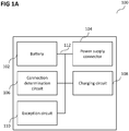
- FIG. 1A shows a computing device 100 (for example a wearable, in other words: a wearable device) according to various embodiments.
- the computing device 100 may include a battery 102.
- the computing device 100 may further include a power supply connector 104 (which for example may be configured to receive power supply from an external source, for example from a power supply device like illustrated in FIG. 1C ).
- the computing device 100 may further include a connection determination circuit 106 configured to determine an input connected to the power supply connector.
- the computing device 100 may further include a charging circuit 108 configured to charge the battery 102 if the connection determination circuit determines a first input connected to the power supply connector.
- the computing device 100 may further include an exception circuit 110 configured to instruct the computing device 100 to perform exception processing if the connection determination circuit determines a second input connected to the power supply connector .
- the battery 102, the power supply connector 104, the connection determination circuit 106, the charging circuit 108, and the exception circuit 110 may be coupled with each other, like indicated by lines 112, for example electrically coupled, for example using a line or a cable, and/ or mechanically coupled.
- the computing device 100 may perform charging or an exception processing, based on the input provided to the power supply connector 104.
- the connection determination circuit 106 may include or may be a voltage polarity determination circuit (not shown in FIG. 1A ) configured to determine a polarity of a power supply connected to the power supply connector 104.
- the first input may include or may be a power supply of a first polarity.
- the second input may include or may be a power supply of a second polarity.
- the charging circuit 108 may be configured to charge the battery 102 if the voltage polarity determination circuit determines a first polarity of the power supply
- the exception circuit 110 may be configured to instruct the computing device 100 to perform exception processing if the voltage polarity determination circuit determines a second polarity of the power supply.
- the first polarity may be inverted compared to the second polarity (in other words: may be opposing to the second polarity).
- the first polarity of the power supply may include or may be a plus pole of the power supply provided to the first contact and a negative pole of the power supply provided to the second contact.
- the second polarity of the power supply may include or may be a negative pole of the power supply provided to the first contact and a plus pole of the power supply provided to the second contact.
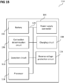
- FIG. 1B shows a computing device 114 (for example a wearable, in other words: a wearable device) according to various embodiments.
- the computing device 114 may, similar to the computing device 100 of FIG. 1A , include a battery 102.
- the computing device 114 may, similar to the computing device 100 of FIG. 1A , further include a power supply connector 104.
- the computing device 114 may, similar to the computing device 100 of FIG. 1A , further include a connection determination circuit 106 configured to determine a polarity of the power supply.
- the computing device 114 may, similar to the computing device 100 of FIG.
- the computing device 114 may, similar to the computing device 100 of FIG. 1A , further include an exception circuit 110 configured to instruct the computing device 114 to perform exception processing if the voltage polarity determination circuit 106 determines a second polarity of the power supply.
- the computing device 114 may further include a reverse voltage protection circuit 116, like will be described in more detail below.
- the computing device 114 may further include a processor 118, like will be described in more detail below.
- the battery 102, the power supply connector 104, the voltage polarity determination circuit 106, the charging circuit 108, the exception circuit 110, the reverse voltage protection circuit 116, and the processor 118 may be coupled with each other, like indicated by lines 120, for example electrically coupled, for example using a line or a cable, and/ or mechanically coupled.
- the reverse voltage protection circuit 116 may be configured to protect the computing device 114 from damage due to a voltage of the second polarity.
- the connection determination circuit 106 may include or may be a short circuit determination circuit (not shown in FIG. 1B ) configured to determine whether a short circuit is provided at the power supply connector 104.
- the first input may include or may be an input different from a short circuit.
- the second input may include or may be a short circuit.
- the charging circuit 108 may be configured to charge the battery 102 if the short circuit determination circuit determines that a voltage different from a short circuit is provided at the power supply connector 104
- the exception circuit 110 may be configured to instruct the computing device 100 to perform exception processing if the short circuit determination circuit determines that a short circuit is provided at the power supply connector 104.
- the exception processing may include or may be or may be included in shutting down the computing device 100.
- the exception processing may include or may be or may be included in restarting the computing device.
- the power supply connector 104 may include or may be or may be included in a plurality of contacts.
- the power supply connector 104 may include or may be or may be included in a first contact and a second contact.
- the exception circuit 110 may include a delay circuit configured to delay the exception processing by a pre-determined amount of time.
- the exception processing may include or may be or may be included in a reset of the processor 118.
- FIG. 1C shows a power supply device 122 according to various embodiments.
- the power supply device 122 may include a power output connector 124.
- the power supply device 122 may further include a switch 126 (for example a mechanical switch or for example an electronic switch) configured to switch between a first state in which the power output connector 124 outputs an output for charging a computing device and a second state in which the power output connector 124 outputs an output for initiating exception processing in the computing device.
- the power output connector 124 and the switch 126 may be coupled with each other, like indicated by line 128, for example electrically coupled, for example using a line or a cable, and/ or mechanically coupled.
- the power output connector 124 may be configured to output a voltage of a first polarity in the first state and to output a voltage of a second polarity in the second state.
- the power output connector 124 may include or may be or may be included in a first contact and a second contact.
- the voltage of the first polarity may include or may be a plus pole at the first contact and a negative pole at the second contact.
- the voltage of the second polarity may include or may be a negative pole at the first contact and a negative pole at the second contact.
- the power output connector 124 may be configured to output a predetermined voltage in the first state and to output a short circuit in the second state.
- FIG. 1D shows a flow diagram 130 illustrating a method for controlling a computing device.
- an input connected to a power supply connector of the computing device may be determined.
- a battery of the computing device may be charged if a first input connected to the power supply connector is determined.
- exception processing may be performed if a second input connected to the power supply connector is determined.
- determining the input may include or may be determining a polarity of a power supply connected to the power supply connector.
- the first input may include or may be a power supply of a first polarity.
- the second input may include or may be a power supply of a second polarity.
- the first polarity may be inverted compared to the second polarity.
- the method may further include protecting the computing device from damage due to a voltage of the second polarity.
- determining the input may include or may be determining whether a short circuit is provided at the power supply connector.
- the first input may include or may be an input different from a short circuit.
- the second input may include or may be a short circuit.
- the exception processing may include or may be or may be included in shutting down the computing device.
- the exception processing may include or may be or may be included in restarting the computing device.
- the power supply connector may include or may be or may be included in a plurality of contacts.
- the power supply connector may include or may be or may be included in a first contact and a second contact.
- the first polarity of the power supply may include or may be a plus pole of the power supply provided to the first contact and a negative pole of the power supply provided to the second contact.
- the second polarity of the power supply may include or may be a negative pole of the power supply provided to the first contact and a plus pole of the power supply provided to the second contact.
- the exception processing may be carried out after a delay of a pre-determined amount of time.
- the exception processing may include or may be or may be included in a reset of a processor of the computing device.
- FIG. IE shows a flow diagram 140 illustrating a method for controlling a power supply device.
- it may be switched, for example using a switch on the power supply device, between a first state in which a power output connector of the power supply device outputs an output for charging a computing device and a second state in which the power output connector outputs an output for initiating exception processing in the computing device.
- the power output connector may output a voltage of a first polarity in the first state and may output a voltage of a second polarity in the second state
- the power output connector may include or may be or may be included in a first contact and a second contact.
- the voltage of the first polarity may include or may be a plus pole at the first contact and a negative pole at the second contact.
- the voltage of the second polarity may include or may be a negative pole at the first contact and a negative pole at the second contact.
- the power output connector may output a predetermined voltage in the first state and may output a short circuit in the second state.
- FIG. 2 shows an illustration 200 of a system with a device 202 (for example a computing device like illustrated in FIG. 1A or like illustrated in FIG. 1B ) and a charging connector 204 (for example a power supply device like illustrated in FIG. 1C ) according to various embodiments.
- a device 202 for example a computing device like illustrated in FIG. 1A or like illustrated in FIG. 1B
- a charging connector 204 for example a power supply device like illustrated in FIG. 1C .
- a circuitry may be provided to allow the same contact pins that are used for charging to perform (or to trigger or to initiate or to instruct or to start) a forced shutdown or reset on a main circuit board of the device 202.
- a reverse voltage may be applied to charging pins 206 of the device to achieve a forced shutdown on the main circuit board.
- the circuitry (for example reverse voltage detection circuit 210 and reset/ shutdown circuit 212) may be further paired with a delay timer reset IC (integrated circuit) to achieve delayed timing reset.
- a charging cable with a built in voltage reversal switch may provide the reverse voltage to trigger the forced shutdown/reset function.
- the device 202 may further include a reverse voltage protection circuit 208.
- a wearable device may be connected to a charging cable (for example live charging cable) with a built-in voltage reversal momentary switch in order to perform a forced shutdown/reset action.
- a charging cable for example live charging cable
- a built-in voltage reversal momentary switch in order to perform a forced shutdown/reset action.
- a voltage reversal switch may be provided (for example on the charging cable), and when the voltage reversal switch is depressed, the following actions may be performed:
- a short pins forced shutdown/reset function on a two-pin charging port for wearables may be provided.
- circuitry may be provided to allow the same contact pins that are used for charging to perform a forced shutdown or reset on the main circuit board of the wearable device. This may be achieved by shorting the charging pins.
- the circuitry may be further paired with a delay timer reset IC to provide delayed timing RESET.
- the charging pins may be shorted with a conductive material (e.g. a pair of stainless steel tweezers) or a specially built charging cable with a momentarily push switch that disconnects the device's charging pins from the charging power source and then shorts the charging pins.
- the device may then go into reset/shutdown immediately or in the case of the usage of a reset/shutdown timer, go into reset/shutdown after time out.
- FIG. 3 shows an illustration 300 of a device 302 according to various embodiments.
- the device 302 may include charging pins 304, a charging pins short circuit detection circuit 306, and a reset/ shutdown circuitry 308 (which may include a timer).
Description
- Various embodiments generally relate to computing devices, power supply devices, methods for controlling a computing device, and methods for controlling a power supply device.
- A forced shutdown function or a force reset function is very commonly found on smart electronic devices that are running complex algorithms. However, in commonly used devices, complex user interaction may be required to trigger such a forced shutdown function or forced reset function. Thus, there may be a need for improved devices.
- The invention is as set out in the independent device claims 1 and 7 and independent method claims 9 and 14. Any disclosed embodiment not covered by the claims, is not part of the invention.
- According to various embodiments, a computing device may be provided. The computing device may include: a battery; a power supply connector; a connection determination circuit configured to determine an input connected to the power supply connector; a charging circuit configured to charge the battery if the connection determination circuit determines a first input connected to the power supply connector; and an exception circuit configured to instruct the computing device to perform exception processing if the connection determination circuit determines a second input connected to the power supply connector.
- According to various embodiments, a power supply device may be provided. The power supply device may include: a power output connector; and a switch configured to switch between a first state in which the power output connector outputs an output for charging a computing device and a second state in which the power output connector outputs an output for initiating exception processing in the computing device.
- According to various embodiments, a method for controlling a computing device may be provided. The method may include: determining an input connected to a power supply connector of the computing device; charging a battery a first input connected to the power supply connector is determined; and performing exception processing if a second input connected to the power supply connector is determined.
- According to various embodiments, a method for controlling a power supply device may be provided. The method may include switching, using a switch, between a first state in which a power output connector of the power supply device outputs an output for charging a computing device and a second state in which the power output connector outputs an output for initiating exception processing in the computing device.
- Related prior art is disclosed in
US2010/277224 andUS2005/007711 . - In the drawings, like reference characters generally refer to the same parts throughout the different views. The drawings are not necessarily to scale, emphasis instead generally being placed upon illustrating the principles of the invention. The dimensions of the various features or elements may be arbitrarily expanded or reduced for clarity. In the following description, various embodiments of the invention are described with reference to the following drawings, in which:
-
FIG. 1A shows a computing device according to various embodiments; -
FIG. 1B shows a computing device according to various embodiments; -
FIG. 1C shows a power supply device according to various embodiments; - FIG. ID shows a flow diagram illustrating a method for controlling a computing device;
- FIG. IE shows a flow diagram illustrating a method for controlling a power supply device;
-
FIG. 2 shows an illustration of a system with a device and a charging connector according to various embodiments; and -
FIG. 3 shows a device according to various embodiments. - The following detailed description refers to the accompanying drawings that show, by way of illustration, specific details and embodiments in which the invention may be practiced. These embodiments are described in sufficient detail to enable those skilled in the art to practice the invention. Other embodiments may be utilized and structural, and logical changes may be made without departing from the scope of the invention. The various embodiments are not necessarily mutually exclusive, as some embodiments can be combined with one or more other embodiments to form new embodiments.
- In this context, the computing device as described in this description may include a memory which is for example used in the processing carried out in the computing device. In this context, the power supply device as described in this description may include a memory which is for example used in the processing carried out in the power supply device. A memory used in the embodiments may be a volatile memory, for example a DRAM (Dynamic Random Access Memory) or a non-volatile memory, for example a PROM (Programmable Read Only Memory), an EPROM (Erasable PROM), EEPROM (Electrically Erasable PROM), or a flash memory, e.g., a floating gate memory, a charge trapping memory, an MRAM (Magnetoresistive Random Access Memory) or a PCRAM (Phase Change Random Access Memory).
- In an embodiment, a "circuit" may be understood as any kind of a logic implementing entity, which may be special purpose circuitry or a processor executing software stored in a memory, firmware, or any combination thereof. Thus, in an embodiment, a "circuit" may be a hard-wired logic circuit or a programmable logic circuit such as a programmable processor, e.g. a microprocessor (e.g. a Complex Instruction Set Computer (CISC) processor or a Reduced Instruction Set Computer (RISC) processor). A "circuit" may also be a processor executing software, e.g. any kind of computer program, e.g. a computer program using a virtual machine code such as e.g. Java. Any other kind of implementation of the respective functions which will be described in more detail below may also be understood as a "circuit" in accordance with an alternative embodiment.
- In the specification the term "comprising" shall be understood to have a broad meaning similar to the term "including" and will be understood to imply the inclusion of a stated integer or step or group of integers or steps but not the exclusion of any other integer or step or group of integers or steps. This definition also applies to variations on the term "comprising" such as "comprise" and "comprises".
- The reference to any prior art in this specification is not, and should not be taken as an acknowledgement or any form of suggestion that the referenced prior art forms part of the common general knowledge in Australia (or any other country).
- In order that the invention may be readily understood and put into practical effect, particular embodiments will now be described by way of examples and not limitations, and with reference to the figures.
- Various embodiments are provided for devices, and various embodiments are provided for methods. It will be understood that basic properties of the devices also hold for the methods and vice versa. Therefore, for sake of brevity, duplicate description of such properties may be omitted.
- It will be understood that any property described herein for a specific device may also hold for any device described herein. It will be understood that any property described herein for a specific method may also hold for any method described herein. Furthermore, it will be understood that for any device or method described herein, not necessarily all the components or steps described must be enclosed in the device or method, but only some (but not all) components or steps may be enclosed.
- The term "coupled" (or "connected") herein may be understood as electrically coupled or as mechanically coupled, for example attached or fixed or attached, or just in contact without any fixation, and it will be understood that both direct coupling or indirect coupling (in other words: coupling without direct contact) may be provided.
- A forced shutdown function or a force reset function is very commonly found on smart electronic devices that are running complex algorithms. However, in commonly used devices, complex user interaction may be required to trigger such a forced shutdown function or forced reset function. According to various embodiments, improved devices may be provided. According to various embodiments, forced shutdown/ reset functions may be provided on a wearable (in other words: on a wearable device).
- According to various embodiments, a reverse voltage forced shutdown/reset function on a two contact (for example two pin) charging port for wearables may be provided.
- Various embodiments may provide a forced shutdown/reset function on wearables, such as the Nabu X, for example by running a reverse voltage through charging contacts (for example charging pins) which are normally used for recharging, without any user input interface (e.g. without any push button). Such embodiments may be suited for button-less wearables (in other words: wearables that have no buttons and switches) that require frequent firmware (FW) updates which a failed update may put the device into a hang state. This may improve user experience as such a function (or circuit) may empower the user to perform a forced shutdown/reset (for example directly) on the device.
-
FIG. 1A shows a computing device 100 (for example a wearable, in other words: a wearable device) according to various embodiments. Thecomputing device 100 may include abattery 102. Thecomputing device 100 may further include a power supply connector 104 (which for example may be configured to receive power supply from an external source, for example from a power supply device like illustrated inFIG. 1C ). Thecomputing device 100 may further include aconnection determination circuit 106 configured to determine an input connected to the power supply connector. Thecomputing device 100 may further include acharging circuit 108 configured to charge thebattery 102 if the connection determination circuit determines a first input connected to the power supply connector. Thecomputing device 100 may further include anexception circuit 110 configured to instruct thecomputing device 100 to perform exception processing if the connection determination circuit determines a second input connected to the power supply connector . Thebattery 102, thepower supply connector 104, theconnection determination circuit 106, the chargingcircuit 108, and theexception circuit 110 may be coupled with each other, like indicated bylines 112, for example electrically coupled, for example using a line or a cable, and/ or mechanically coupled. - In other words, the
computing device 100 may perform charging or an exception processing, based on the input provided to thepower supply connector 104. - According to various embodiments, the
connection determination circuit 106 may include or may be a voltage polarity determination circuit (not shown inFIG. 1A ) configured to determine a polarity of a power supply connected to thepower supply connector 104. According to various embodiments, the first input may include or may be a power supply of a first polarity. According to various embodiments, the second input may include or may be a power supply of a second polarity. In other words, the chargingcircuit 108 may be configured to charge thebattery 102 if the voltage polarity determination circuit determines a first polarity of the power supply, and theexception circuit 110 may be configured to instruct thecomputing device 100 to perform exception processing if the voltage polarity determination circuit determines a second polarity of the power supply. - According to various embodiments, the first polarity may be inverted compared to the second polarity (in other words: may be opposing to the second polarity).
- According to various embodiments, the first polarity of the power supply may include or may be a plus pole of the power supply provided to the first contact and a negative pole of the power supply provided to the second contact.
- According to various embodiments, the second polarity of the power supply may include or may be a negative pole of the power supply provided to the first contact and a plus pole of the power supply provided to the second contact.
-
FIG. 1B shows a computing device 114 (for example a wearable, in other words: a wearable device) according to various embodiments. Thecomputing device 114 may, similar to thecomputing device 100 ofFIG. 1A , include abattery 102. Thecomputing device 114 may, similar to thecomputing device 100 ofFIG. 1A , further include apower supply connector 104. Thecomputing device 114 may, similar to thecomputing device 100 ofFIG. 1A , further include aconnection determination circuit 106 configured to determine a polarity of the power supply. Thecomputing device 114 may, similar to thecomputing device 100 ofFIG. 1A , further include acharging circuit 108 configured to charge thebattery 102 if the voltagepolarity determination circuit 106 determines a first polarity of the power supply. Thecomputing device 114 may, similar to thecomputing device 100 ofFIG. 1A , further include anexception circuit 110 configured to instruct thecomputing device 114 to perform exception processing if the voltagepolarity determination circuit 106 determines a second polarity of the power supply. Thecomputing device 114 may further include a reversevoltage protection circuit 116, like will be described in more detail below. Thecomputing device 114 may further include aprocessor 118, like will be described in more detail below. Thebattery 102, thepower supply connector 104, the voltagepolarity determination circuit 106, the chargingcircuit 108, theexception circuit 110, the reversevoltage protection circuit 116, and theprocessor 118 may be coupled with each other, like indicated bylines 120, for example electrically coupled, for example using a line or a cable, and/ or mechanically coupled. - According to various embodiments, the reverse
voltage protection circuit 116 may be configured to protect thecomputing device 114 from damage due to a voltage of the second polarity. - According to various embodiments, the
connection determination circuit 106 may include or may be a short circuit determination circuit (not shown inFIG. 1B ) configured to determine whether a short circuit is provided at thepower supply connector 104. According to various embodiments, the first input may include or may be an input different from a short circuit. According to various embodiments, the second input may include or may be a short circuit. In other words, the chargingcircuit 108 may be configured to charge thebattery 102 if the short circuit determination circuit determines that a voltage different from a short circuit is provided at thepower supply connector 104, and theexception circuit 110 may be configured to instruct thecomputing device 100 to perform exception processing if the short circuit determination circuit determines that a short circuit is provided at thepower supply connector 104. - According to various embodiments, the exception processing may include or may be or may be included in shutting down the
computing device 100. - According to various embodiments, the exception processing may include or may be or may be included in restarting the computing device.
- According to various embodiments, the
power supply connector 104 may include or may be or may be included in a plurality of contacts. - According to various embodiments, the
power supply connector 104 may include or may be or may be included in a first contact and a second contact. - According to various embodiments, the
exception circuit 110 may include a delay circuit configured to delay the exception processing by a pre-determined amount of time. - According to various embodiments, the exception processing may include or may be or may be included in a reset of the
processor 118. -
FIG. 1C shows apower supply device 122 according to various embodiments. Thepower supply device 122 may include apower output connector 124. Thepower supply device 122 may further include a switch 126 (for example a mechanical switch or for example an electronic switch) configured to switch between a first state in which thepower output connector 124 outputs an output for charging a computing device and a second state in which thepower output connector 124 outputs an output for initiating exception processing in the computing device. Thepower output connector 124 and theswitch 126 may be coupled with each other, like indicated byline 128, for example electrically coupled, for example using a line or a cable, and/ or mechanically coupled. - According to various embodiments, the
power output connector 124 may be configured to output a voltage of a first polarity in the first state and to output a voltage of a second polarity in the second state. - According to various embodiments, the
power output connector 124 may include or may be or may be included in a first contact and a second contact. - According to various embodiments, the voltage of the first polarity may include or may be a plus pole at the first contact and a negative pole at the second contact.
- According to various embodiments, the voltage of the second polarity may include or may be a negative pole at the first contact and a negative pole at the second contact.
- According to various embodiments, the
power output connector 124 may be configured to output a predetermined voltage in the first state and to output a short circuit in the second state. -
FIG. 1D shows a flow diagram 130 illustrating a method for controlling a computing device. In 132, an input connected to a power supply connector of the computing device may be determined. In 134, a battery of the computing device may be charged if a first input connected to the power supply connector is determined. In 136, exception processing may be performed if a second input connected to the power supply connector is determined. - According to various embodiments, determining the input may include or may be determining a polarity of a power supply connected to the power supply connector. According to various embodiments, the first input may include or may be a power supply of a first polarity. According to various embodiments, the second input may include or may be a power supply of a second polarity.
- According to various embodiments, the first polarity may be inverted compared to the second polarity.
- According to various embodiments, the method may further include protecting the computing device from damage due to a voltage of the second polarity.
- According to various embodiments, determining the input may include or may be determining whether a short circuit is provided at the power supply connector. According to various embodiments, the first input may include or may be an input different from a short circuit. According to various embodiments, the second input may include or may be a short circuit.
- According to various embodiments, the exception processing may include or may be or may be included in shutting down the computing device.
- According to various embodiments, the exception processing may include or may be or may be included in restarting the computing device.
- According to various embodiments, the power supply connector may include or may be or may be included in a plurality of contacts.
- According to various embodiments, the power supply connector may include or may be or may be included in a first contact and a second contact.
- According to various embodiments, the first polarity of the power supply may include or may be a plus pole of the power supply provided to the first contact and a negative pole of the power supply provided to the second contact.
- According to various embodiments, the second polarity of the power supply may include or may be a negative pole of the power supply provided to the first contact and a plus pole of the power supply provided to the second contact.
- According to various embodiments, the exception processing may be carried out after a delay of a pre-determined amount of time.
- According to various embodiments, the exception processing may include or may be or may be included in a reset of a processor of the computing device.
- FIG. IE shows a flow diagram 140 illustrating a method for controlling a power supply device. In 142, it may be switched, for example using a switch on the power supply device, between a first state in which a power output connector of the power supply device outputs an output for charging a computing device and a second state in which the power output connector outputs an output for initiating exception processing in the computing device.
- According to various embodiments, the power output connector may output a voltage of a first polarity in the first state and may output a voltage of a second polarity in the second state
- According to various embodiments, the power output connector may include or may be or may be included in a first contact and a second contact.
- According to various embodiments, the voltage of the first polarity may include or may be a plus pole at the first contact and a negative pole at the second contact.
- According to various embodiments, the voltage of the second polarity may include or may be a negative pole at the first contact and a negative pole at the second contact.
- According to various embodiments, the power output connector may output a predetermined voltage in the first state and may output a short circuit in the second state.
-
FIG. 2 shows anillustration 200 of a system with a device 202 (for example a computing device like illustrated inFIG. 1A or like illustrated inFIG. 1B ) and a charging connector 204 (for example a power supply device like illustrated inFIG. 1C ) according to various embodiments. - According to various embodiments, a circuitry may be provided to allow the same contact pins that are used for charging to perform (or to trigger or to initiate or to instruct or to start) a forced shutdown or reset on a main circuit board of the
device 202. A reverse voltage may be applied to chargingpins 206 of the device to achieve a forced shutdown on the main circuit board. The circuitry (for example reversevoltage detection circuit 210 and reset/ shutdown circuit 212) may be further paired with a delay timer reset IC (integrated circuit) to achieve delayed timing reset. A charging cable with a built in voltage reversal switch may provide the reverse voltage to trigger the forced shutdown/reset function. Thedevice 202 may further include a reversevoltage protection circuit 208. - According to various embodiments, a wearable device may be connected to a charging cable (for example live charging cable) with a built-in voltage reversal momentary switch in order to perform a forced shutdown/reset action.
- According to various embodiments, a voltage reversal switch may be provided (for example on the charging cable), and when the voltage reversal switch is depressed, the following actions may be performed:
- 1. The "reverse voltage" protection circuit may kick in to protect the main circuitry from reversed voltage damage.
- 2. The "reverse voltage" detection circuit may activate the reset/shutdown circuitry.
- 3. The device may then go into reset/shutdown immediately or in the case of the usage of a reset/shutdown timer, go into reset/shutdown after time out.
- According to various embodiments, a short pins forced shutdown/reset function on a two-pin charging port for wearables (in other words: wearable devices) may be provided.
- According to various embodiments, circuitry may be provided to allow the same contact pins that are used for charging to perform a forced shutdown or reset on the main circuit board of the wearable device. This may be achieved by shorting the charging pins. The circuitry may be further paired with a delay timer reset IC to provide delayed timing RESET.
- To perform a reset, the charging pins may be shorted with a conductive material (e.g. a pair of stainless steel tweezers) or a specially built charging cable with a momentarily push switch that disconnects the device's charging pins from the charging power source and then shorts the charging pins. The device may then go into reset/shutdown immediately or in the case of the usage of a reset/shutdown timer, go into reset/shutdown after time out.
-
FIG. 3 shows anillustration 300 of adevice 302 according to various embodiments. Thedevice 302 may include chargingpins 304, a charging pins shortcircuit detection circuit 306, and a reset/ shutdown circuitry 308 (which may include a timer). - While the invention has been particularly shown and described with reference to specific embodiments, it should be understood by those skilled in the art that various changes in form and detail may be made therein without departing from the scope of the invention as defined by the appended claims. The scope of the invention is thus indicated by the appended claims.
Claims (15)
- A computing device (100) comprising:a battery (102);a power supply connector (104) comprising a first contact and a second contact;a connection determination circuit (106) configured to determine an input connected to the power supply connector (104);a charging circuit (108) configured to charge the battery (102) if the connection determination circuit (106) determines a first input connected to the power supply connector (104); andan exception circuit (110) configured to instruct the computing device (100) to perform exception processing if the connection determination circuit (106) determines a second input connected to the power supply connector (104);wherein the first input is from a first input group and is a voltage for charging the battery (102); andwherein the second input is from a second input group and is a short circuit caused by a conductive member arranged between the first contact and the second contact.
- The computing device (100) of claim 1,
wherein the connection determination circuit (106) comprises a voltage polarity determination circuit configured to determine a polarity of a power supply connected to the power supply connector (104);
wherein the first input group further comprises a power supply of a first polarity and the second input group further comprises a power supply of a second polarity;
wherein the first polarity is inverted compared to the second polarity;
wherein the first polarity of the power supply comprises a plus pole of the power supply provided to a first contact and a negative pole of the power supply provided to a second contact; and
wherein the second polarity of the power supply comprises a negative pole of the power supply provided to the first contact and a plus pole of the power supply provided to the second contact. - The computing device (100) of claim 2, further comprising:
a reverse voltage protection circuit (116) configured to protect the computing device (100) from damage due to a voltage of the second polarity. - The computing device (100) of any one of claims 1 to 3,
wherein the exception processing comprises shutting down the computing device (100) or restarting the computing device (100); and
wherein optionally the exception circuit (110) comprises a delay circuit configured to delay the exception processing by a pre-determined amount of time. - The computing device (100) of any one of claims 1 to 4,
wherein the power supply connector (104) comprises a plurality of contacts. - The computing device (100) of any one of claims 1 to 5, further comprising:a processor (118);wherein the exception processing comprises a reset of the processor (118).
- A power supply device (122) comprising:a power output connector (124) connectable to charging pins of a computing device (100); anda switch (126) configured to switch between a first state, from a first state group, in which the power output connector connects a power source to charging pins of the computing device (100) for charging the computing device (100) and a second state, from a second state group, in which the switch (126) disconnects the power output connector (124) from the charging pins and shorts the charging pins for initiating exception processing in the computing device (100);wherein the switch (126) comprises a conductive member, wherein the switch (126) shorts the charging pins by arranging the conductive member between the charging pins.
- The power supply device (122) of claim 7,
wherein the power output connector (124) is configured to output a voltage of a first polarity in a further state from the first state group and to output a voltage of a second polarity in a further state from the second state group;
wherein the power output connector (124) comprises a first contact and a second contact;
wherein the voltage of the first polarity comprises a plus pole at the first contact and a negative pole at the second contact; and
wherein the voltage of the second polarity comprises a negative pole at the first contact and a negative pole at the second contact. - A method for controlling a computing device, the method comprising:determining an input connected to a power supply connector of the computing device (132), wherein the power supply connector comprises a first contact and a second contact;charging the battery if a first input connected to the power supply connector is determined (134);performing exception processing if a second input connected to the power supply connector is determined (136);wherein the first input is from a first input group and is a voltage for charging the battery; andwherein the second input is from a second input group and is a short circuit between the first contact and the second contact; andproviding the second input by arranging a conductive member between the first contact and the second contact.
- The method of claim 9,
wherein determining the input comprises determining a polarity of a power supply connected to the power supply connector;
wherein the first input group further comprises a power supply of a first polarity and the second input group further comprises a power supply of a second polarity;
wherein the first polarity is inverted compared to the second polarity;
wherein the first polarity of the power supply comprises a plus pole of the power supply provided to the first contact and a negative pole of the power supply provided to the second contact; and
wherein the second polarity of the power supply comprises a negative pole of the power supply provided to the first contact and a plus pole of the power supply provided to the second contact. - The method of claim 10, further comprising:
protecting the computing device from damage due to a voltage of the second polarity. - The method of any one of claims 9 to 11,
wherein the exception processing comprises shutting down the computing device or restarting the computing device;
wherein optionally the exception processing is carried out after a delay of a pre-determined amount of time. - The method of any one of claims 9 to 12,
wherein the exception processing comprises a reset of a processor of the computing device. - A method for controlling a power supply device, the method comprising:
switching, using a switch, between a first state, from a first state group, in which a power output connector of the power supply device connects a power source to charging pins of a computing device for charging the computing device and a second state, from a second state group, in which the switch disconnects the power output connector from the charging pins and shorts the charging pins with a conductive member of the switch for initiating exception processing in the computing device. - The method of claim 14,
wherein the power output connector outputs a voltage of a first polarity in a further state from the first state group and outputs a voltage of a second polarity in a further state from the second state group;
wherein the power output connector comprises a first contact and a second contact;
wherein the voltage of the first polarity comprises a plus pole at the first contact and a negative pole at the second contact; and
wherein the voltage of the second polarity comprises a negative pole at the first contact and a negative pole at the second contact.
Applications Claiming Priority (1)
| Application Number | Priority Date | Filing Date | Title |
|---|---|---|---|
| PCT/SG2016/050110 WO2017155462A1 (en) | 2016-03-09 | 2016-03-09 | Computing devices, power supply devices, methods for controlling a computing device, and methods for controlling a power supply device |
Publications (3)
| Publication Number | Publication Date |
|---|---|
| EP3427124A1 EP3427124A1 (en) | 2019-01-16 |
| EP3427124A4 EP3427124A4 (en) | 2019-03-13 |
| EP3427124B1 true EP3427124B1 (en) | 2021-08-04 |
Family
ID=59790665
Family Applications (1)
| Application Number | Title | Priority Date | Filing Date |
|---|---|---|---|
| EP16893721.7A Active EP3427124B1 (en) | 2016-03-09 | 2016-03-09 | Computing devices, power supply devices, methods for controlling a computing device, and methods for controlling a power supply device |
Country Status (7)
| Country | Link |
|---|---|
| US (1) | US20200097058A1 (en) |
| EP (1) | EP3427124B1 (en) |
| CN (1) | CN108780345B (en) |
| AU (1) | AU2016396983B2 (en) |
| SG (1) | SG11201807462VA (en) |
| TW (1) | TWI735540B (en) |
| WO (1) | WO2017155462A1 (en) |
Families Citing this family (1)
| Publication number | Priority date | Publication date | Assignee | Title |
|---|---|---|---|---|
| US11152935B2 (en) | 2018-08-28 | 2021-10-19 | Google Llc | System and method to deliver reset via power line |
Family Cites Families (16)
| Publication number | Priority date | Publication date | Assignee | Title |
|---|---|---|---|---|
| US7106566B2 (en) * | 2003-07-08 | 2006-09-12 | Arques Technology | Power adapter interface circuitry for protecting a battery operated system |
| US7668572B2 (en) * | 2004-10-15 | 2010-02-23 | Proxim Wireless Corporation | System and method of polarity reversal for reload detection |
| DE102007026786A1 (en) * | 2006-08-21 | 2008-04-03 | Continental Teves Ag & Co. Ohg | Active sensor for use as wheel rotational speed sensor in motor vehicle, has changeover module that changes between normal operating mode and special operating mode by reversal of polarity of supply voltage present at connections |
| JP4573884B2 (en) * | 2008-06-18 | 2010-11-04 | 三菱電機株式会社 | In-vehicle electronic control unit power failure detection circuit |
| US8283899B2 (en) * | 2008-11-04 | 2012-10-09 | Broadcom Corporation | Reducing current leakage and improving shelf life time of battery-based-devices |
| CN101989751B (en) * | 2009-07-30 | 2014-01-15 | 宏达国际电子股份有限公司 | Power supply device, portable electronic device and related judgment method |
| JP5575506B2 (en) * | 2010-02-26 | 2014-08-20 | 三洋電機株式会社 | Vehicle power supply device and vehicle equipped with the power supply device |
| US8667882B1 (en) * | 2011-05-06 | 2014-03-11 | Rock River Arms, Inc. | Firearm |
| US8542472B2 (en) * | 2011-07-26 | 2013-09-24 | Apple Inc. | Protection circuitry for reversible connectors |
| CN104737381B (en) * | 2012-10-18 | 2017-09-22 | 惠普发展公司,有限责任合伙企业 | The Polarity Control of flat connector |
| US9153986B1 (en) * | 2014-04-15 | 2015-10-06 | Fuelbox, Inc. | Versatile plug and play charging station |
| TWI531133B (en) * | 2014-05-02 | 2016-04-21 | 宏碁股份有限公司 | Charging method and electronic device |
| US9448605B2 (en) * | 2014-08-29 | 2016-09-20 | Zippy Technology Corp. | Redundant power supply system providing rapid start of backup |
| CN104978300B (en) * | 2015-07-16 | 2019-04-12 | Oppo广东移动通信有限公司 | Mobile terminal and its detection method being connect with external equipment and device |
| CN105138101A (en) * | 2015-08-31 | 2015-12-09 | 联想(北京)有限公司 | Power supply method and electronic devices |
| CN105322397B (en) * | 2015-10-13 | 2018-01-23 | 深圳市祝你快乐科技有限公司 | USB port connector and its implementation with charging protection function |
-
2016
- 2016-03-09 WO PCT/SG2016/050110 patent/WO2017155462A1/en active Application Filing
- 2016-03-09 CN CN201680083360.XA patent/CN108780345B/en active Active
- 2016-03-09 US US16/083,387 patent/US20200097058A1/en not_active Abandoned
- 2016-03-09 AU AU2016396983A patent/AU2016396983B2/en active Active
- 2016-03-09 SG SG11201807462VA patent/SG11201807462VA/en unknown
- 2016-03-09 EP EP16893721.7A patent/EP3427124B1/en active Active
-
2017
- 2017-02-20 TW TW106105585A patent/TWI735540B/en active
Also Published As
| Publication number | Publication date |
|---|---|
| US20200097058A1 (en) | 2020-03-26 |
| AU2016396983A1 (en) | 2018-09-20 |
| AU2016396983B2 (en) | 2021-12-16 |
| TWI735540B (en) | 2021-08-11 |
| WO2017155462A1 (en) | 2017-09-14 |
| CN108780345B (en) | 2022-07-08 |
| CN108780345A (en) | 2018-11-09 |
| TW201734704A (en) | 2017-10-01 |
| EP3427124A4 (en) | 2019-03-13 |
| SG11201807462VA (en) | 2018-09-27 |
| EP3427124A1 (en) | 2019-01-16 |
Similar Documents
| Publication | Publication Date | Title |
|---|---|---|
| JP6626882B2 (en) | Charge control method and device, and electronic equipment | |
| EP2624407B1 (en) | Method and apparatus for charging battery | |
| JP2008091085A (en) | Battery pack and electronic equipment | |
| US20200103471A1 (en) | Apparatus and method for testing adaptor | |
| CN106292341A (en) | A kind of power on/off system and method | |
| TW201622292A (en) | Portable electronic device and charging method therefor | |
| JP5982692B2 (en) | Charge / discharge management device and mobile terminal | |
| CN104536551A (en) | Method and device for clearing away information on complementary metal oxide semiconductor (CMOS) | |
| EP3427124B1 (en) | Computing devices, power supply devices, methods for controlling a computing device, and methods for controlling a power supply device | |
| WO2020088388A1 (en) | Charging control circuit, charging circuit and charging control method | |
| CN108170211B (en) | Camera power-on driving method and electronic terminal | |
| CN107678871B (en) | Electronic equipment starting method and electronic equipment | |
| US20170256935A1 (en) | System reset for a portable apparatus | |
| TW201431245A (en) | Charging system and charging method thereof | |
| CN102073575A (en) | Management engine state detection circuit | |
| TWI528683B (en) | End of discharge point automatic adjusting circuit for battery management chip | |
| CN104485699B (en) | The battery capacity protection circuit of portable equipment | |
| US20200272591A1 (en) | Port circuit, method for supplying power for electronic device via port circuit and electronic device | |
| CN210405082U (en) | Electronic equipment | |
| CN202798057U (en) | Manually switched battery circuit | |
| CN105701425A (en) | Electronic equipment, and mainboard and protection circuit thereof | |
| CN108628724A (en) | A kind of method and terminal of display charge information | |
| CN105162241A (en) | Detection processing method and apparatus of terminal device | |
| CN101847042B (en) | Write-protection device for flash memory | |
| KR100548261B1 (en) | Charge terminal protection apparatus for embedded terminal |
Legal Events
| Date | Code | Title | Description |
|---|---|---|---|
| STAA | Information on the status of an ep patent application or granted ep patent |
Free format text: STATUS: THE INTERNATIONAL PUBLICATION HAS BEEN MADE |
|
| PUAI | Public reference made under article 153(3) epc to a published international application that has entered the european phase |
Free format text: ORIGINAL CODE: 0009012 |
|
| STAA | Information on the status of an ep patent application or granted ep patent |
Free format text: STATUS: REQUEST FOR EXAMINATION WAS MADE |
|
| 17P | Request for examination filed |
Effective date: 20180831 |
|
| AK | Designated contracting states |
Kind code of ref document: A1 Designated state(s): AL AT BE BG CH CY CZ DE DK EE ES FI FR GB GR HR HU IE IS IT LI LT LU LV MC MK MT NL NO PL PT RO RS SE SI SK SM TR |
|
| AX | Request for extension of the european patent |
Extension state: BA ME |
|
| A4 | Supplementary search report drawn up and despatched |
Effective date: 20190211 |
|
| RIC1 | Information provided on ipc code assigned before grant |
Ipc: G06F 1/24 20060101ALI20190205BHEP Ipc: G06F 1/26 20060101AFI20190205BHEP Ipc: H02J 7/00 20060101ALI20190205BHEP Ipc: G06F 1/16 20060101ALI20190205BHEP |
|
| STAA | Information on the status of an ep patent application or granted ep patent |
Free format text: STATUS: REQUEST FOR EXAMINATION WAS MADE |
|
| DAV | Request for validation of the european patent (deleted) | ||
| DAX | Request for extension of the european patent (deleted) | ||
| GRAP | Despatch of communication of intention to grant a patent |
Free format text: ORIGINAL CODE: EPIDOSNIGR1 |
|
| STAA | Information on the status of an ep patent application or granted ep patent |
Free format text: STATUS: GRANT OF PATENT IS INTENDED |
|
| INTG | Intention to grant announced |
Effective date: 20210315 |
|
| GRAS | Grant fee paid |
Free format text: ORIGINAL CODE: EPIDOSNIGR3 |
|
| GRAA | (expected) grant |
Free format text: ORIGINAL CODE: 0009210 |
|
| STAA | Information on the status of an ep patent application or granted ep patent |
Free format text: STATUS: THE PATENT HAS BEEN GRANTED |
|
| AK | Designated contracting states |
Kind code of ref document: B1 Designated state(s): AL AT BE BG CH CY CZ DE DK EE ES FI FR GB GR HR HU IE IS IT LI LT LU LV MC MK MT NL NO PL PT RO RS SE SI SK SM TR |
|
| REG | Reference to a national code |
Ref country code: GB Ref legal event code: FG4D |
|
| REG | Reference to a national code |
Ref country code: AT Ref legal event code: REF Ref document number: 1417640 Country of ref document: AT Kind code of ref document: T Effective date: 20210815 |
|
| REG | Reference to a national code |
Ref country code: CH Ref legal event code: EP |
|
| REG | Reference to a national code |
Ref country code: DE Ref legal event code: R096 Ref document number: 602016061810 Country of ref document: DE |
|
| REG | Reference to a national code |
Ref country code: IE Ref legal event code: FG4D |
|
| RAP4 | Party data changed (patent owner data changed or rights of a patent transferred) |
Owner name: RAZER (ASIA-PACIFIC) PTE. LTD. |
|
| REG | Reference to a national code |
Ref country code: LT Ref legal event code: MG9D |
|
| REG | Reference to a national code |
Ref country code: NL Ref legal event code: MP Effective date: 20210804 |
|
| REG | Reference to a national code |
Ref country code: AT Ref legal event code: MK05 Ref document number: 1417640 Country of ref document: AT Kind code of ref document: T Effective date: 20210804 |
|
| PG25 | Lapsed in a contracting state [announced via postgrant information from national office to epo] |
Ref country code: SE Free format text: LAPSE BECAUSE OF FAILURE TO SUBMIT A TRANSLATION OF THE DESCRIPTION OR TO PAY THE FEE WITHIN THE PRESCRIBED TIME-LIMIT Effective date: 20210804 Ref country code: RS Free format text: LAPSE BECAUSE OF FAILURE TO SUBMIT A TRANSLATION OF THE DESCRIPTION OR TO PAY THE FEE WITHIN THE PRESCRIBED TIME-LIMIT Effective date: 20210804 Ref country code: NO Free format text: LAPSE BECAUSE OF FAILURE TO SUBMIT A TRANSLATION OF THE DESCRIPTION OR TO PAY THE FEE WITHIN THE PRESCRIBED TIME-LIMIT Effective date: 20211104 Ref country code: PT Free format text: LAPSE BECAUSE OF FAILURE TO SUBMIT A TRANSLATION OF THE DESCRIPTION OR TO PAY THE FEE WITHIN THE PRESCRIBED TIME-LIMIT Effective date: 20211206 Ref country code: HR Free format text: LAPSE BECAUSE OF FAILURE TO SUBMIT A TRANSLATION OF THE DESCRIPTION OR TO PAY THE FEE WITHIN THE PRESCRIBED TIME-LIMIT Effective date: 20210804 Ref country code: FI Free format text: LAPSE BECAUSE OF FAILURE TO SUBMIT A TRANSLATION OF THE DESCRIPTION OR TO PAY THE FEE WITHIN THE PRESCRIBED TIME-LIMIT Effective date: 20210804 Ref country code: ES Free format text: LAPSE BECAUSE OF FAILURE TO SUBMIT A TRANSLATION OF THE DESCRIPTION OR TO PAY THE FEE WITHIN THE PRESCRIBED TIME-LIMIT Effective date: 20210804 Ref country code: LT Free format text: LAPSE BECAUSE OF FAILURE TO SUBMIT A TRANSLATION OF THE DESCRIPTION OR TO PAY THE FEE WITHIN THE PRESCRIBED TIME-LIMIT Effective date: 20210804 Ref country code: AT Free format text: LAPSE BECAUSE OF FAILURE TO SUBMIT A TRANSLATION OF THE DESCRIPTION OR TO PAY THE FEE WITHIN THE PRESCRIBED TIME-LIMIT Effective date: 20210804 Ref country code: BG Free format text: LAPSE BECAUSE OF FAILURE TO SUBMIT A TRANSLATION OF THE DESCRIPTION OR TO PAY THE FEE WITHIN THE PRESCRIBED TIME-LIMIT Effective date: 20211104 |
|
| PG25 | Lapsed in a contracting state [announced via postgrant information from national office to epo] |
Ref country code: PL Free format text: LAPSE BECAUSE OF FAILURE TO SUBMIT A TRANSLATION OF THE DESCRIPTION OR TO PAY THE FEE WITHIN THE PRESCRIBED TIME-LIMIT Effective date: 20210804 Ref country code: LV Free format text: LAPSE BECAUSE OF FAILURE TO SUBMIT A TRANSLATION OF THE DESCRIPTION OR TO PAY THE FEE WITHIN THE PRESCRIBED TIME-LIMIT Effective date: 20210804 Ref country code: GR Free format text: LAPSE BECAUSE OF FAILURE TO SUBMIT A TRANSLATION OF THE DESCRIPTION OR TO PAY THE FEE WITHIN THE PRESCRIBED TIME-LIMIT Effective date: 20211105 |
|
| PG25 | Lapsed in a contracting state [announced via postgrant information from national office to epo] |
Ref country code: NL Free format text: LAPSE BECAUSE OF FAILURE TO SUBMIT A TRANSLATION OF THE DESCRIPTION OR TO PAY THE FEE WITHIN THE PRESCRIBED TIME-LIMIT Effective date: 20210804 |
|
| PG25 | Lapsed in a contracting state [announced via postgrant information from national office to epo] |
Ref country code: DK Free format text: LAPSE BECAUSE OF FAILURE TO SUBMIT A TRANSLATION OF THE DESCRIPTION OR TO PAY THE FEE WITHIN THE PRESCRIBED TIME-LIMIT Effective date: 20210804 |
|
| REG | Reference to a national code |
Ref country code: DE Ref legal event code: R097 Ref document number: 602016061810 Country of ref document: DE |
|
| PG25 | Lapsed in a contracting state [announced via postgrant information from national office to epo] |
Ref country code: SM Free format text: LAPSE BECAUSE OF FAILURE TO SUBMIT A TRANSLATION OF THE DESCRIPTION OR TO PAY THE FEE WITHIN THE PRESCRIBED TIME-LIMIT Effective date: 20210804 Ref country code: SK Free format text: LAPSE BECAUSE OF FAILURE TO SUBMIT A TRANSLATION OF THE DESCRIPTION OR TO PAY THE FEE WITHIN THE PRESCRIBED TIME-LIMIT Effective date: 20210804 Ref country code: RO Free format text: LAPSE BECAUSE OF FAILURE TO SUBMIT A TRANSLATION OF THE DESCRIPTION OR TO PAY THE FEE WITHIN THE PRESCRIBED TIME-LIMIT Effective date: 20210804 Ref country code: EE Free format text: LAPSE BECAUSE OF FAILURE TO SUBMIT A TRANSLATION OF THE DESCRIPTION OR TO PAY THE FEE WITHIN THE PRESCRIBED TIME-LIMIT Effective date: 20210804 Ref country code: CZ Free format text: LAPSE BECAUSE OF FAILURE TO SUBMIT A TRANSLATION OF THE DESCRIPTION OR TO PAY THE FEE WITHIN THE PRESCRIBED TIME-LIMIT Effective date: 20210804 Ref country code: AL Free format text: LAPSE BECAUSE OF FAILURE TO SUBMIT A TRANSLATION OF THE DESCRIPTION OR TO PAY THE FEE WITHIN THE PRESCRIBED TIME-LIMIT Effective date: 20210804 |
|
| PLBE | No opposition filed within time limit |
Free format text: ORIGINAL CODE: 0009261 |
|
| STAA | Information on the status of an ep patent application or granted ep patent |
Free format text: STATUS: NO OPPOSITION FILED WITHIN TIME LIMIT |
|
| 26N | No opposition filed |
Effective date: 20220506 |
|
| PG25 | Lapsed in a contracting state [announced via postgrant information from national office to epo] |
Ref country code: IT Free format text: LAPSE BECAUSE OF FAILURE TO SUBMIT A TRANSLATION OF THE DESCRIPTION OR TO PAY THE FEE WITHIN THE PRESCRIBED TIME-LIMIT Effective date: 20210804 |
|
| PG25 | Lapsed in a contracting state [announced via postgrant information from national office to epo] |
Ref country code: SI Free format text: LAPSE BECAUSE OF FAILURE TO SUBMIT A TRANSLATION OF THE DESCRIPTION OR TO PAY THE FEE WITHIN THE PRESCRIBED TIME-LIMIT Effective date: 20210804 |
|
| PG25 | Lapsed in a contracting state [announced via postgrant information from national office to epo] |
Ref country code: MC Free format text: LAPSE BECAUSE OF FAILURE TO SUBMIT A TRANSLATION OF THE DESCRIPTION OR TO PAY THE FEE WITHIN THE PRESCRIBED TIME-LIMIT Effective date: 20210804 |
|
| REG | Reference to a national code |
Ref country code: CH Ref legal event code: PL |
|
| REG | Reference to a national code |
Ref country code: BE Ref legal event code: MM Effective date: 20220331 |
|
| PG25 | Lapsed in a contracting state [announced via postgrant information from national office to epo] |
Ref country code: LU Free format text: LAPSE BECAUSE OF NON-PAYMENT OF DUE FEES Effective date: 20220309 Ref country code: LI Free format text: LAPSE BECAUSE OF NON-PAYMENT OF DUE FEES Effective date: 20220331 Ref country code: IE Free format text: LAPSE BECAUSE OF NON-PAYMENT OF DUE FEES Effective date: 20220309 Ref country code: CH Free format text: LAPSE BECAUSE OF NON-PAYMENT OF DUE FEES Effective date: 20220331 |
|
| PG25 | Lapsed in a contracting state [announced via postgrant information from national office to epo] |
Ref country code: BE Free format text: LAPSE BECAUSE OF NON-PAYMENT OF DUE FEES Effective date: 20220331 |
|
| PGFP | Annual fee paid to national office [announced via postgrant information from national office to epo] |
Ref country code: FR Payment date: 20230320 Year of fee payment: 8 |
|
| PGFP | Annual fee paid to national office [announced via postgrant information from national office to epo] |
Ref country code: GB Payment date: 20230323 Year of fee payment: 8 Ref country code: DE Payment date: 20230227 Year of fee payment: 8 |
|
| P01 | Opt-out of the competence of the unified patent court (upc) registered |
Effective date: 20230327 |
|
| PG25 | Lapsed in a contracting state [announced via postgrant information from national office to epo] |
Ref country code: HU Free format text: LAPSE BECAUSE OF FAILURE TO SUBMIT A TRANSLATION OF THE DESCRIPTION OR TO PAY THE FEE WITHIN THE PRESCRIBED TIME-LIMIT; INVALID AB INITIO Effective date: 20160309 |