EP3425541B1 - Verfahren zur erzeugung eines 3d-schaltungslayouts aus einem 2d-schaltungslayout - Google Patents
Verfahren zur erzeugung eines 3d-schaltungslayouts aus einem 2d-schaltungslayout Download PDFInfo
- Publication number
- EP3425541B1 EP3425541B1 EP18181802.2A EP18181802A EP3425541B1 EP 3425541 B1 EP3425541 B1 EP 3425541B1 EP 18181802 A EP18181802 A EP 18181802A EP 3425541 B1 EP3425541 B1 EP 3425541B1
- Authority
- EP
- European Patent Office
- Prior art keywords
- circuit
- cells
- row
- rows
- level
- Prior art date
- Legal status (The legal status is an assumption and is not a legal conclusion. Google has not performed a legal analysis and makes no representation as to the accuracy of the status listed.)
- Active
Links
Images

Classifications
-
- G—PHYSICS
- G06—COMPUTING OR CALCULATING; COUNTING
- G06F—ELECTRIC DIGITAL DATA PROCESSING
- G06F30/00—Computer-aided design [CAD]
- G06F30/30—Circuit design
- G06F30/39—Circuit design at the physical level
- G06F30/392—Floor-planning or layout, e.g. partitioning or placement
-
- G—PHYSICS
- G06—COMPUTING OR CALCULATING; COUNTING
- G06F—ELECTRIC DIGITAL DATA PROCESSING
- G06F2119/00—Details relating to the type or aim of the analysis or the optimisation
- G06F2119/18—Manufacturability analysis or optimisation for manufacturability
-
- Y—GENERAL TAGGING OF NEW TECHNOLOGICAL DEVELOPMENTS; GENERAL TAGGING OF CROSS-SECTIONAL TECHNOLOGIES SPANNING OVER SEVERAL SECTIONS OF THE IPC; TECHNICAL SUBJECTS COVERED BY FORMER USPC CROSS-REFERENCE ART COLLECTIONS [XRACs] AND DIGESTS
- Y02—TECHNOLOGIES OR APPLICATIONS FOR MITIGATION OR ADAPTATION AGAINST CLIMATE CHANGE
- Y02P—CLIMATE CHANGE MITIGATION TECHNOLOGIES IN THE PRODUCTION OR PROCESSING OF GOODS
- Y02P90/00—Enabling technologies with a potential contribution to greenhouse gas [GHG] emissions mitigation
- Y02P90/02—Total factory control, e.g. smart factories, flexible manufacturing systems [FMS] or integrated manufacturing systems [IMS]
Definitions
- the present disclosure relates to the field of 3D circuit designs, and in particular to a method and computing device for generating a 3D circuit layout from a 2D circuit layout.
- a key phase of the design process is the operation known as "place and route".
- a GDS (graphic database system) file of the circuit design is generated by a dedicated conception tool prior to fabrication.
- the conception tool first places the cells of the circuit design on the available surface of the integrated circuit, and then a routing algorithm is applied that interconnects the cells of the circuit design in order to create a circuit layout.
- 3D circuits in which cells are positioned on multiple stacked levels interconnected by 3D vias, provide many advantages in terms of circuit compactness and performance.
- monolithic 3D transistor technology also known as sequential 3D and CoolCubeTM, involves the fabrication of a plurality of layers of transistors as a single block.
- two or more layers or tiers of transistors are formed sequentially, and interconnected by vertical 3D vias.
- this technology is described in more detail in the publication by P. Batude et al. entitled "3D sequential integration opportunities and technology optimization", IEEE International Interconnect Technology Conference, 2014, pages 373-376 .
- An advantage of monolithic 3D technology with respect to other 3D technologies is that the process allows a high density of interconnections (small size and spacing of the vias) when compared with TSVs (Through-Silicon-Vias) or face-to-face contact (copper to copper). Furthermore, 3D fabrication processes that involve stacking two or more integrated circuits suffer from problems of alignment, contrary to the monolithic 3D approach in which the device is fabricated sequentially.
- a problem for 3D circuit design is that existing software tools implementing place and route have been developed for 2D circuits, and are not compatible with the generation of high-density 3D circuit designs. Furthermore, creating a new design tool configured for 3D circuit design would be time consuming and costly.
- the term "around”, preceding a value is used to indicate a tolerance of plus or minus 10 percent of the value in question.
- Figure 1 is a cross-section view of a monolithic 3D circuit 100 according to an example embodiment.
- the circuit 100 for example comprises a transistor level 102 formed on a handle layer 101, and a further transistor level 104 superposed over the transistor level 102.
- An intermediate metal interconnection layer 106 for example serves to provide interconnections between transistor devices 108 of the levels 102, 104. While not illustrated in Figure 1 , a further metal interconnection layer could be provided above the transistor level 104.
- Examples of 3D vias 110, 112 are also illustrated, known as a monolithic inter-tier vias (MIV).
- MIV monolithic inter-tier vias
- a monolithic inter-tier via has the advantage of being of significantly smaller dimensions than a TSV (Through-Silicon-Via).
- a TSV typically has a diameter of around 1000 times that of a transistor
- an MIV for example has a diameter of the same order of magnitude as that of the vias in the metal layer, for example of around 40 nm for 14 nm technology, or more generally a diameter of between 35 and 120 nm.
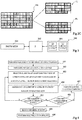
- Figures 2A to 2C represent plan views of circuit layouts during a method of conception of a 3D circuit, such as a monolithic 3D circuit, according to example embodiment of the present disclosure.
- This design process is for example implemented by a suitable computing device, such as the one of Figure 3 , as will now be described.
- Figure 3 schematically illustrates a computing device 300 adapted to implement a method of 3D circuit conception.
- the device 300 for example comprises one or more processors (P) 302 under control of instructions stored in an instruction memory (INSTR MEM) 304.
- a memory 306 for example stores a 2D circuit layout (2D CIRCUIT LAYOUT), and a 3D circuit layout (3D CIRCUIT LAYOUT) generated based on the 2D circuit layout.
- the memories 304 and 306 could be implemented in a same memory device or in separate memory devices.
- the computing device 300 could additionally comprise one or more user input devices, such as a keyboard, mouse, etc., one or more output devices such as a display, and/or a communications interface permitting the generated 3D circuit layout to be transmitted to a manufacturing plant for fabrication.
- user input devices such as a keyboard, mouse, etc.
- output devices such as a display
- communications interface permitting the generated 3D circuit layout to be transmitted to a manufacturing plant for fabrication.
- Figure 4 is a flow diagram illustrating operations in a method of conception of a 3D circuit according to an embodiment of the present disclosure. The method is for example implemented by the device of Figure 3 .
- a 2D circuit layout 200 is for example generated using a placement operation, corresponding to a first phase of a place and route operation.
- the 2D circuit layout 200 comprises 33 standard cells numbered "1" to "33". Rows 1 to 6 of the 2D circuit layout respectively comprise: the cells “1" to "4"; the cells “5" to “10”; the cells “11” to “16”; the cells “17” to “21”; the cells “22” to “28”; and the cells “29” to “33".
- Each of the standard cells for example has equal height H, but varying widths. In the example of Figure 2A , these standard cells are arranged in 6 rows of equal height H.
- the 2D circuit layout 200 is for example formed of columns and rows of elementary sites, each elementary site being of the same height H and a same width W.
- Each of the standard cells occupies an integer number of these elementary sites in the row direction.
- the 2D circuit layout has a width equal to 10 elementary sites, with each standard cell having a width of between 1 and 4 elementary sites, in other words a width of between W and 4W.
- the cells “1", “27” and “30” have a width of 4 elementary sites
- the cells “3", “8”, “11” and “29” have a width of 3 elementary sites
- the cells “4", "5", “10”, “13”, “14” and “17” to “21” have a width of 2 elementary sites
- the remaining cells have a width of a single elementary site.
- the 2D circuit layout could have different dimensions, and comprise a different number of standard cells, for example hundreds or thousands of standard cells.
- an empty 3D circuit layout of N levels is for example generated, where N is for example an integer equal to 2 or more.
- N is for example an integer equal to 2 or more.
- each level initially has a same number of rows as the 2D circuit layout 200, and each row for example has the same number of elementary sites as the rows of the 2D circuit layout 200.
- a selection is made, among at least one first row of a first of the levels of the 3D circuit layout and at least one second row of a second of the levels of the 3D circuit layout, of the row having the most available free space, in other words the most number of free elementary sites.
- a cell of a current M rows of the 2D circuit layout is then assigned to the row selected in operation 403, where M is a positive integer, and is for example equal to between 1 and 10.
- M is a positive integer, and is for example equal to between 1 and 10.
- the M rows are for example successive rows of the 2D circuit layout.
- an operation 405 it is then determined whether there are further unassigned cells in the current M rows of the 2D circuit layout, and if so, operations 403 and 404 are repeated. If not, in an operation 406, it is determined whether there is an unassigned group of M rows in the 2D circuit layout, and if so, in an operation 407 the current M rows is updated to be the further unassigned M rows, and operations 403 to 405 are repeated until all cells of all rows of the 2D circuit layout have been assigned to rows of the 3D circuit layout.
- FIG. 2A An example of the cell assignment of operations 403 to 407 is represented in Figure 2A .
- the 3D circuit layout comprises two levels, a top level TL and a bottom level BL.
- the 3D circuit design method described herein could be used to generate 3D circuit designs having any number of levels.
- each level TL, BL of the 3D circuit layout for example has the same dimensions as the 2D circuit layout.
- M is equal to 1, and each cell of each row of the 2D circuit layout is assigned to one or the other of a corresponding row in the top level TL and a corresponding row in the bottom level BL.
- cells of the 2D circuit layout 200 are assigned row by row starting with the top row in the figure, and the rows are processed from left to right.
- the assignment algorithm for example involves assigning a cell in a row r of the 2D circuit layout to a corresponding row r of the top level TL or bottom level BL based on which of these rows has the most available elementary sites, in other words the fewest occupied elementary sites.
- priority is for example given to one of the levels, and to the top level in the example of the first row of Figure 2A .
- the standard cells "1" and "4" of row 1 of the 2D circuit layout 200 are assigned to row 1 of the top level TL, and the standard cells “2" and “3” of row 1 of the 2D circuit layout 200 are assigned to row 1 of the bottom level BL. Furthermore, the cells “5" and “8” of row 2 of the 2D circuit layout are assigned to row 2 of the top level TL, and the cells “6", "7", “9” and “10” are assigned to row 2 of the bottom level BL.
- the number of rows in each level of the 3D circuit layout is for example reduced. However, as described in more detail below, depending on how row assignment is performed, in some cases row reduction is not needed.
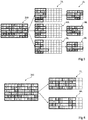
- Figure 2B represents an example of a row reduction phase for the top and bottom levels represented in Figure 2A , and in which the number of rows of the top and bottom levels of the 3D circuit layout is reduced from 6 to 4. More generally, the number of rows is for example reduced by around a third in the case that there are two levels in the 3D circuit layout. This is for example achieved by grouping the rows of each level in groups of three adjacent rows, and emptying the cells from the middle row of each group, allowing the emptied middle row to then be suppressed.
- Figure 2B represents the row reduction applied to the top level TL.
- a first view V1 of the top level TL corresponds to the arrangement of cells following the level assignment of Figure 2A .
- Row emptying is for example performed based on the following algorithm:
- the middle row MR1 of the first group of three rows which is row 2 of the top level TL, is emptied by inserting the standard cell "8" between the standard cells "11” and “14” in row 3 of the top level TL, and by inserting the standard cell "5" between the standard cells "1” and "4" in row 1 of the top level TL.
- the middle row MR2 of the second group of three rows is emptied in a similar fashion.
- a view V2 in Figure 2B illustrates the top level TL once all of the middle rows have been emptied.
- the rows MR1 and MR2 are empty. These empty rows are then for example removed entirely by bringing together the occupied rows, as shown by a view V3 in Figure 2B .
- empty columns of elementary sites are also for example removed.
- Figure 2C illustrates both the top level TL and bottom level BL resulting from the cell assignment and row reduction phases of Figures 2A and 2B .
- the resulting 3D circuit comprises, in each level, standard cells occupying two-thirds the number of rows of the original 2D circuit layout, and for example between 60 and 80 percent of the width of the original 2D circuit layout. Furthermore, the cells that were close in the original 2D circuit layout remain close, either in the same level, or in an adjacent level, in the 3D circuit layout.
- routing is for example performed between the circuit cells of each level and between the levels of the 3D circuit layout.
- a 3D circuit in accordance with the 3D circuit layout is then for example fabricated.
- files defining the 3D circuit layout are transmitted to a manufacturing plant such that 3D circuits may be fabricated based on the circuit layout.
- These files for example include a GDS file representing the 3D circuit layout.
- circuit cells each circuit cell corresponding to a single standard cell, or to a group of more than one standard cell.
- the circuit cells for example have a common height, e.g. a height equal to a same integer number of elementary sites.
- the cells of the top level and bottom level have the same height and width as the corresponding cells of the 2D circuit layout
- the cells of the top level could be enlarged with respect to those of the bottom level in order to provide additional room for forming vertical 3D vias, for example of the type described in the United States Patent US 8,710,671 .
- one or more additional specific circuit cells could be assigned to the second level and/or to higher levels of the 3D circuit layout, these specific circuit cells corresponding to zones in which vias to lower levels can be formed.
- each of the levels of the 3D circuit layout is empty before the cell assignment operations 403 to 407
- one or more circuits of the 2D circuit layout are placed on a corresponding level before the assignment operations. For example, it may be decided that certain macros, such as a memory or other IP, or a packet of standard cells, should be assigned to a certain level rather than having their standard cells divided between levels. The assignment operations then proceed while taking into account the fact that some rows already have occupied elementary sites.
- Figure 5 illustrates an example in which the method of Figure 4 is applied to generate, based on the same 2D circuit layout 200 of Figure 2A , a 3D circuit layout having three levels, a top level TL, a middle level ML, and a bottom level BL. This is achieved using the method described above in relation to Figure 4 in which the cell assignment operations 402 and 403 involve assigning cells to each of three levels rather than two levels.
- the rows of the 2D circuit layout are for example grouped into a number of two level and three level groups, and a two level or three level approach is then applied to each group.
- Figure 6 is based on the same 2D circuit layout 200 as used in the previous embodiments.
- the 3D circuit layout is generated by filling up top and bottom levels already having a reduced number of rows with respect to the 2D circuit layout.
- the top and bottom levels each has just 4 rows.
- the cells of the 2D circuit design are for example assigned in groups of three rows, in other words the parameter M of operation 404 of Figure 4 is equal to 3.
- the cells are for example assigned by assigning the remaining cell that is most to the left and closest to the top of the group of M rows.
- the cells in the first three rows of the layout 200 are for example assigned in the order "1", "5", "6", “7", etc. through to "16".
- Each cell is for example assigned to one of the first two rows of the top level TL or one of the top two rows of the bottom level BL based on the row having the most available elementary sites.
- preference is for example given in the following order, from highest to lowest: first row of top level; first row of bottom level; second row of top level; second row of bottom level.
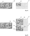
- Figure 7A illustrates an example of a first cell assignment operation.
- the example is based on the same 2D circuit layout 200 as in previous examples.
- the cells "1" to "33" of the 2D layout are now considered to be sub-cells of larger cells.
- a dashed rectangle 702 for example designates a zone corresponding to a default size of each of the cells to be defined. This zone initially designates a first cell having several sub-cells "1", "5", "6" and "11” falling therein. Furthermore, all sub-cells having at least one elementary site falling within the rectangle 702 are for example considered to form part of the cell.
- the rectangle 702 is for example enlarged to form a cell 702' including the whole of cell "1", and also including the cells "7" and "12". Further cells are then for example defined in a similar manner.
- Figure 7B illustrates top level TL and bottom level BL following several further cell assignments.
- a cell 704 consisting of sub-cells “2", “3", “8", “9", “13” and “14” is for example assigned to the bottom level BL;
- a cell 706 consisting of sub-cells "4", “10", “15” and “16” is for example assigned to the top level TL to the right of the cell 702';
- a cell 708 consisting of the sub-cells "17”, “18", “22” to "25” and “29” is for example assigned to the bottom level below the cell 704;
- a cell 710 consisting of the sub-cells "19", "20", “26", “27” and “30” to "32” is for example assigned to the top level below the cell 702';
- a cell 712 consisting of the sub-cells "21", “28” and "33” is for example assigned to the bottom level to the right of the cell 708.
- each level of the 3D circuit layout includes several empty elementary sites in view of the non-rectangular form of some of the cells.
- An advantage of the embodiments described herein is that a 3D circuit layout can be generated by adapting a 2D layout produced using a standard placement algorithm, and while maintaining a form factor that is relatively close to the original. Indeed, other processes for assigning circuit cells to levels of the 3D circuit layout could lead to uneven distribution of the circuit cells among the various rows.
- an advantage of emptying the circuit cells from the row to be emptied in an order opposite to the order that the circuit cells were added to the row to be emptied is that this minimizes the number of circuit cells of adjacent rows that are to be moved in order to make room for the circuit cells of the row to be emptied. Thus this leads to a gain in terms of processing time.
Landscapes
- Engineering & Computer Science (AREA)
- Computer Hardware Design (AREA)
- Physics & Mathematics (AREA)
- Theoretical Computer Science (AREA)
- Architecture (AREA)
- Evolutionary Computation (AREA)
- Geometry (AREA)
- General Engineering & Computer Science (AREA)
- General Physics & Mathematics (AREA)
- Design And Manufacture Of Integrated Circuits (AREA)
Claims (14)
- Ein Verfahren zum Erzeugen eines 3D-Schaltungslayouts auf der Grundlage eines 2D-Schaltungslayouts durch eine Rechenvorrichtung (300), wobei das Verfahren Folgendes aufweist
Durchführen einer Platzierungsoperation an einem 2D-Schaltungsentwurf durch die Rechenvorrichtung (300), um ein 2D-Schaltungslayout (200) zu erzeugen, das R Reihen von Schaltungszellen aufweist, wobei R eine ganze Zahl ist, die mindestens gleich drei ist;
Zuweisen einiger der Schaltungszellen einer ersten Gruppe von Schaltungszellen des 2D-Schaltungslayouts zu einer oder mehreren ersten Reihen einer ersten Ebene des 3D-Schaltungslayouts und einiger der Schaltungszellen der ersten Gruppe von Schaltungszellen zu einer oder mehreren ersten Reihen einer zweiten Ebene des 3D-Schaltungslayouts durch die Rechenvorrichtung (300), wobei die erste Gruppe den Schaltungszellen einer ersten Zeile des 2D-Schaltungslayouts oder den Schaltungszellen einer Mehrzahl von ersten aufeinanderfolgenden Zeilen des 2D-Schaltungslayouts entspricht; und
Zuweisen einiger der Schaltungszellen einer zweiten Gruppe von Schaltungszellen des 2D-Schaltungslayouts zu einer oder mehreren zweiten Reihen der ersten Ebene des 3D-Schaltungslayouts und einiger der Schaltungszellen der zweiten Gruppe von Schaltungszellen zu einer oder mehreren zweiten Reihen der zweiten Ebene des 3D-Schaltungslayouts durch die Rechenvorrichtung (300), wobei die zweite Gruppe den Schaltungszellen einer zweiten Reihe des 2D-Schaltungslayouts oder den Schaltungszellen einer Vielzahl von zweiten aufeinanderfolgenden Reihen des 2D-Schaltungslayouts entspricht,
wobei das Zuweisen jeder Schaltungszelle der ersten Gruppe durchgeführt wird durch:Auswählen der Reihe mit dem größten verfügbaren Platz unter mindestens einer der ersten Reihen jeder der ersten und zweiten Ebenen; undZuweisen der Schaltungszelle der ersten Gruppe zu der ausgewählten Reihe; undwobei das Zuweisen jeder Schaltungszelle der zweiten Gruppe durchgeführt wird durch:Auswählen der Reihe mit dem größten verfügbaren Platz unter mindestens einer der zweiten Reihen jeder der ersten und zweiten Ebenen; undZuweisen der Schaltungszelle der zweiten Gruppe zu der ausgewählten Reihe;wobei das Verfahren ferner das Übertragen des 3D-Schaltungslayouts an eine Fertigungsanlage zur Herstellung aufweist. - Verfahren nach Anspruch 1, wobei jede der ersten und zweiten Ebenen des 3D-Schaltungslayouts anfänglich dieselbe Anzahl von Zeilen aufweist wie das 2D-Schaltungslayout, und jede Zelle der ersten Gruppe von Schaltungszellen einer entsprechenden Zeile der ersten oder zweiten Ebene zugeordnet wird.
- Verfahren nach Anspruch 2, das ferner, nachdem alle Schaltungszellen des 2D-Schaltungslayouts den Ebenen des 3D-Schaltungslayouts zugewiesen wurden, Folgendes aufweist:Verringern der Anzahl der Zeilen der ersten Ebene des 3D-Schaltungslayouts durch Leeren der Schaltungszellen aus mindestens einer Zeile und Unterdrücken der mindestens einen Zeile, wobei die geleerten Schaltungszellen in eine der an die geleerte Zeile angrenzenden Zeilen in der ersten Ebene verschoben werden; undVerringern der Anzahl von Zeilen der zweiten Ebene des 3D-Schaltungslayouts durch Leeren der Schaltungszellen aus mindestens einer Zeile und Unterdrücken der mindestens einen Zeile, wobei die geleerten Schaltungszellen in eine oder zwei an die geleerte Zeile angrenzende Zeilen in der zweiten Ebene verschoben werden.
- Verfahren nach Anspruch 3, wobei:das Leeren der Schaltungszellen, um die Anzahl der Reihen der ersten Ebene zu verringern, das Bewegen der Zellen aus der zu leerenden Reihe der ersten Ebene in der entgegengesetzten Reihenfolge zu einer Reihenfolge aufweist, in der die Zellen zu der zu leerenden Reihe der ersten Ebene hinzugefügt wurden; unddas Leeren der Schaltkreiszellen, um die Anzahl der Reihen der zweiten Ebene zu reduzieren, das Bewegen der Zellen von der zu leerenden Reihe der zweiten Ebene in der entgegengesetzten Reihenfolge zu einer Reihenfolge aufweist, in der die Zellen zu der zu leerenden Reihe der zweiten Ebene hinzugefügt wurden.
- Verfahren nach Anspruch 1, wobei der Schritt des Auswählens der Reihe mit dem größten verfügbaren Platz unter mindestens einer der ersten Reihen den Vergleich des verfügbaren Platzes in allen ersten Reihen der ersten und zweiten Ebene und das Auswählen der Reihe mit dem größten verfügbaren Platz aufweist.
- Verfahren nach einem der Ansprüche 1 bis 5, wobei jede der Schaltungszellen aus einer Vielzahl von Unterzellen besteht.
- Verfahren nach einem der Ansprüche 1 bis 6, wobei während der Zuweisungsoperationen eine oder mehrere spezifische Schaltungszellen der zweiten Ebene oder einer höheren Ebene des 3D-Schaltungslayouts zugewiesen werden, wobei die eine oder mehreren spezifischen Schaltungszellen Zonen zum Bilden von Durchkontaktierungen oder Vias zu niedrigeren Ebenen des 3D-Schaltungslayouts entsprechen.
- Verfahren nach einem der Ansprüche 1 bis 7, wobei vor den Zuweisungsoperationen zunächst eine oder mehrere Schaltungen des 2D-Schaltungslayouts einer oder mehreren Ebenen des 3D-Schaltungslayouts zugewiesen werden.
- Computerlesbares Speichermedium, das Computerbefehle speichert, die das Verfahren nach einem der Ansprüche 1 bis 8 implementieren, wenn es von einer Rechenvorrichtung ausgeführt wird.
- Computervorrichtung zum Erzeugen eines 3D-Schaltungslayouts auf der Grundlage eines 2D-Schaltungslayouts, wobei die Computervorrichtung aufweist:eine oder mehrere Speichervorrichtungen (306), die das 2D-Schaltungslayout speichern; undeine Verarbeitungsvorrichtung (302), die konfiguriert ist zum:Durchführen einer Platzierungsoperation an einem 2D-Schaltungsentwurf, um ein 2D-Schaltungslayout (200) zu erzeugen, das R Reihen von Schaltungszellen aufweist, wobei R eine ganze Zahl ist, die mindestens gleich drei ist;Zuweisen einiger der Schaltungszellen einer ersten Gruppe von Schaltungszellen des 2D-Schaltungslayouts zu einer oder mehreren ersten Reihen einer ersten Ebene des 3D-Schaltungslayouts und einiger der Schaltungszellen der ersten Gruppe von Schaltungszellen zu einer oder mehreren ersten Reihen einer zweiten Ebene des 3D-Schaltungslayouts, wobei die erste Gruppe den Schaltungszellen einer ersten Reihe des 2D-Schaltungslayouts oder den Schaltungszellen einer Mehrzahl von ersten aufeinanderfolgenden Reihen des 2D-Schaltungslayouts entspricht; undZuweisen einiger der Schaltungszellen einer zweiten Gruppe von Schaltungszellen des 2D-Schaltungslayouts zu einer oder mehreren zweiten Reihen der ersten Ebene des 3D-Schaltungslayouts und einiger der Schaltungszellen der zweiten Gruppe von Schaltungszellen zu einer oder mehreren zweiten Reihen der zweiten Ebene des 3D-Schaltungslayouts, wobei die zweite Gruppe den Schaltungszellen einer zweiten Reihe des 2D-Schaltungslayouts oder den Schaltungszellen einer Vielzahl von zweiten aufeinanderfolgenden Reihen des 2D-Schaltungslayouts entspricht,wobei die Computervorrichtung (300) konfiguriert ist, um jede Schaltungszelle der ersten Gruppe zuzuweisen durch:Auswählen der Reihe mit dem größten verfügbaren Platz unter mindestens einer der ersten Reihen jeder der ersten und zweiten Ebene; undZuweisen der Schaltungszelle der ersten Gruppe zu der ausgewählten Reihe; undwobei die Computervorrichtung (300) konfiguriert ist, um jede Schaltungszelle der zweiten Gruppe zuzuweisen durch:Auswählen der Reihe mit dem größten verfügbaren Platz unter mindestens einer der zweiten Reihen jeder der ersten und zweiten Ebene; undZuweisen der Schaltungszelle der zweiten Gruppe zu der ausgewählten Reihe;wobei die Rechnereinrichtung ferner so konfiguriert ist, dass sie das 3D-Schaltungslayout an eine Fertigungsanlage zur Herstellung übermittelt.
- Computervorrichtung nach Anspruch 10, wobei die Verarbeitungsvorrichtung (302) ferner so konfiguriert ist, dass sie jede der ersten und zweiten Ebenen des Schaltungslayouts so erzeugt, dass sie anfänglich die gleiche Anzahl von Zeilen wie das 2D-Schaltungslayout aufweist.
- Computervorrichtung nach Anspruch 11, wobei die Verarbeitungsvorrichtung (302) ferner so konfiguriert ist, um nach dem Zuweisen aller Schaltungszellen des 2D-Schaltungslayouts zu Ebenen des 3D-Schaltungslayouts
die Anzahl der Zeilen der ersten Ebene des 3D-Schaltungslayouts zu reduzieren, indem die Schaltungszellen aus mindestens einer Zeile geleert werden und die mindestens eine Zeile unterdrückt wird, wobei die geleerten Schaltungszellen in eine der an die geleerte Zeile angrenzenden Zeilen in der ersten Ebene verschoben werden; und
die Anzahl der Zeilen der zweiten Ebene des 3D-Schaltungslayouts zu reduzieren, indem die Schaltungszellen aus mindestens einer Zeile geleert werden und die mindestens eine Zeile unterdrückt wird, wobei die geleerten Schaltungszellen in eine oder zwei der geleerten Zeile benachbarten Zeilen in der zweiten Ebene verschoben werden. - Computervorrichtung nach Anspruch 12, wobei die Verarbeitungsvorrichtung (302) konfiguriert ist, um:die Schaltungszellen zu leeren, um die Anzahl der Zeilen der ersten Ebene zu reduzieren, indem die Zellen aus der zu leerenden Zeile der ersten Ebene in der entgegengesetzten Reihenfolge zu einer Reihenfolge bewegt werden, in der die Zellen zu der zu leerenden Zeile der ersten Ebene hinzugefügt wurden; unddie Schaltungszellen zu leeren, um die Anzahl der Reihen der zweiten Ebene zu reduzieren, indem die Zellen aus der zu leerenden Reihe der zweiten Ebene in der entgegengesetzten Reihenfolge zu einer Reihenfolge bewegt werden, in der die Zellen zu der zu leerenden Reihe der zweiten Ebene hinzugefügt wurden.
- Computervorrichtung nach einem der Ansprüche 10 bis 13, wobei die Verarbeitungsvorrichtung (302) ferner so konfiguriert ist, dass sie eine oder mehrere spezifische Schaltungszellen der zweiten Ebene oder einer höheren Ebene des 3D-Schaltungslayouts zuweist, wobei die eine oder mehreren spezifischen Schaltungszellen Zonen zum Bilden von Durchkontaktierungen oder Vias zu niedrigeren Ebenen des 3D-Schaltungslayouts entsprechen.
Applications Claiming Priority (1)
| Application Number | Priority Date | Filing Date | Title |
|---|---|---|---|
| FR1756352A FR3068798B1 (fr) | 2017-07-05 | 2017-07-05 | Procede de generation d'un agencement de circuit 3d a partir d'un agencement de circuit 2d |
Publications (2)
| Publication Number | Publication Date |
|---|---|
| EP3425541A1 EP3425541A1 (de) | 2019-01-09 |
| EP3425541B1 true EP3425541B1 (de) | 2021-08-25 |
Family
ID=60302189
Family Applications (1)
| Application Number | Title | Priority Date | Filing Date |
|---|---|---|---|
| EP18181802.2A Active EP3425541B1 (de) | 2017-07-05 | 2018-07-05 | Verfahren zur erzeugung eines 3d-schaltungslayouts aus einem 2d-schaltungslayout |
Country Status (3)
| Country | Link |
|---|---|
| US (1) | US10740528B2 (de) |
| EP (1) | EP3425541B1 (de) |
| FR (1) | FR3068798B1 (de) |
Families Citing this family (3)
| Publication number | Priority date | Publication date | Assignee | Title |
|---|---|---|---|---|
| US10678987B2 (en) * | 2017-10-25 | 2020-06-09 | Taiwan Semiconductor Manufacturing Company Ltd. | Cell layout method and system for creating stacked 3D integrated circuit having two tiers |
| CN111710644B (zh) * | 2020-05-20 | 2022-01-04 | 西南科技大学 | 一种基于硅通孔的三维集成电路布局方法 |
| CN116976269B (zh) * | 2023-08-01 | 2024-09-03 | 北京华大九天科技股份有限公司 | 填充方法及装置、计算装置和存储介质 |
Family Cites Families (5)
| Publication number | Priority date | Publication date | Assignee | Title |
|---|---|---|---|---|
| US6370673B1 (en) * | 1999-03-22 | 2002-04-09 | Synopsys, Inc. | Method and system for high speed detailed placement of cells within an integrated circuit design |
| US7526739B2 (en) * | 2005-07-26 | 2009-04-28 | R3 Logic, Inc. | Methods and systems for computer aided design of 3D integrated circuits |
| EP2469597A3 (de) | 2010-12-23 | 2016-06-29 | Commissariat à l'Énergie Atomique et aux Énergies Alternatives | Mehrstufige integrierte Schaltung, Vorrichtung und Verfahren zur Modellierung von integrierten Schaltungen in mehreren Ebenen |
| US9672312B2 (en) * | 2015-05-04 | 2017-06-06 | Globalfoundries Inc. | Method wherein test cells and dummy cells are included into a layout of an integrated circuit |
| KR102458446B1 (ko) * | 2016-03-03 | 2022-10-26 | 삼성전자주식회사 | 스탠다드 셀을 포함하는 반도체 장치 및 그것의 전자 설계 자동화 방법 |
-
2017
- 2017-07-05 FR FR1756352A patent/FR3068798B1/fr not_active Expired - Fee Related
-
2018
- 2018-07-05 EP EP18181802.2A patent/EP3425541B1/de active Active
- 2018-07-05 US US16/027,545 patent/US10740528B2/en not_active Expired - Fee Related
Non-Patent Citations (1)
| Title |
|---|
| None * |
Also Published As
| Publication number | Publication date |
|---|---|
| FR3068798A1 (fr) | 2019-01-11 |
| US20190012420A1 (en) | 2019-01-10 |
| US10740528B2 (en) | 2020-08-11 |
| FR3068798B1 (fr) | 2021-12-31 |
| EP3425541A1 (de) | 2019-01-09 |
Similar Documents
| Publication | Publication Date | Title |
|---|---|---|
| EP3584724A1 (de) | Konzeption einer 3d-schaltung mit makros | |
| US4593363A (en) | Simultaneous placement and wiring for VLSI chips | |
| US10127344B2 (en) | Automation for monolithic 3D devices | |
| TWI877096B (zh) | 產生三維積體電路設計的方法 | |
| US6473891B1 (en) | Wire routing to control skew | |
| US11030371B2 (en) | Automation for monolithic 3D devices | |
| US5973376A (en) | Architecture having diamond shaped or parallelogram shaped cells | |
| US11106853B1 (en) | Automation for monolithic 3D devices | |
| US10740528B2 (en) | Method of generating a 3D circuit layout from a 2D circuit layout | |
| US20210357568A1 (en) | Design automation for monolithic 3d devices | |
| US5909376A (en) | Physical design automation system and process for designing integrated circuit chips using highly parallel sieve optimization with multiple "jiggles" | |
| CN104752415B (zh) | 用于三维集成电路的方法和装置 | |
| US20220147689A1 (en) | Design automation for monolithic 3d devices | |
| US10831972B2 (en) | Capacity model for global routing | |
| US11514221B2 (en) | Automation for monolithic 3D devices | |
| US11487928B2 (en) | Automation for monolithic 3D devices | |
| US11615228B1 (en) | Automation methods for 3D integrated circuits and devices | |
| CN111753484B (zh) | 一种基于电路性能的多裸片结构fpga的布局方法 | |
| US11574109B1 (en) | Automation methods for 3D integrated circuits and devices | |
| CN111742319B (zh) | 在多芯片集成电路器件中选择布线资源的方法 | |
| US5838585A (en) | Physical design automation system and method using monotonically improving linear clusterization | |
| CN111753486A (zh) | 一种多裸片结构fpga的新型布局方法 | |
| Tabrizi et al. | A fast force-directed simulated annealing for 3D IC partitioning | |
| US11720736B2 (en) | Automation methods for 3D integrated circuits and devices | |
| Zhao et al. | 3D-Flow: Flow-based Standard Cell Legalization for 3D ICs |
Legal Events
| Date | Code | Title | Description |
|---|---|---|---|
| PUAI | Public reference made under article 153(3) epc to a published international application that has entered the european phase |
Free format text: ORIGINAL CODE: 0009012 |
|
| STAA | Information on the status of an ep patent application or granted ep patent |
Free format text: STATUS: REQUEST FOR EXAMINATION WAS MADE |
|
| 17P | Request for examination filed |
Effective date: 20180705 |
|
| AK | Designated contracting states |
Kind code of ref document: A1 Designated state(s): AL AT BE BG CH CY CZ DE DK EE ES FI FR GB GR HR HU IE IS IT LI LT LU LV MC MK MT NL NO PL PT RO RS SE SI SK SM TR |
|
| AX | Request for extension of the european patent |
Extension state: BA ME |
|
| STAA | Information on the status of an ep patent application or granted ep patent |
Free format text: STATUS: EXAMINATION IS IN PROGRESS |
|
| 17Q | First examination report despatched |
Effective date: 20200423 |
|
| REG | Reference to a national code |
Ref country code: DE Ref legal event code: R079 Ref document number: 602018022272 Country of ref document: DE Free format text: PREVIOUS MAIN CLASS: G06F0017500000 Ipc: G06F0119180000 |
|
| RIC1 | Information provided on ipc code assigned before grant |
Ipc: G06F 30/392 20200101ALI20210317BHEP Ipc: G06F 119/18 20200101AFI20210317BHEP |
|
| GRAP | Despatch of communication of intention to grant a patent |
Free format text: ORIGINAL CODE: EPIDOSNIGR1 |
|
| STAA | Information on the status of an ep patent application or granted ep patent |
Free format text: STATUS: GRANT OF PATENT IS INTENDED |
|
| INTG | Intention to grant announced |
Effective date: 20210607 |
|
| GRAS | Grant fee paid |
Free format text: ORIGINAL CODE: EPIDOSNIGR3 |
|
| GRAA | (expected) grant |
Free format text: ORIGINAL CODE: 0009210 |
|
| STAA | Information on the status of an ep patent application or granted ep patent |
Free format text: STATUS: THE PATENT HAS BEEN GRANTED |
|
| AK | Designated contracting states |
Kind code of ref document: B1 Designated state(s): AL AT BE BG CH CY CZ DE DK EE ES FI FR GB GR HR HU IE IS IT LI LT LU LV MC MK MT NL NO PL PT RO RS SE SI SK SM TR |
|
| REG | Reference to a national code |
Ref country code: CH Ref legal event code: EP |
|
| REG | Reference to a national code |
Ref country code: IE Ref legal event code: FG4D Ref country code: AT Ref legal event code: REF Ref document number: 1424536 Country of ref document: AT Kind code of ref document: T Effective date: 20210915 |
|
| REG | Reference to a national code |
Ref country code: DE Ref legal event code: R096 Ref document number: 602018022272 Country of ref document: DE |
|
| REG | Reference to a national code |
Ref country code: LT Ref legal event code: MG9D |
|
| REG | Reference to a national code |
Ref country code: NL Ref legal event code: MP Effective date: 20210825 |
|
| REG | Reference to a national code |
Ref country code: AT Ref legal event code: MK05 Ref document number: 1424536 Country of ref document: AT Kind code of ref document: T Effective date: 20210825 |
|
| PG25 | Lapsed in a contracting state [announced via postgrant information from national office to epo] |
Ref country code: PT Free format text: LAPSE BECAUSE OF FAILURE TO SUBMIT A TRANSLATION OF THE DESCRIPTION OR TO PAY THE FEE WITHIN THE PRESCRIBED TIME-LIMIT Effective date: 20211227 Ref country code: NO Free format text: LAPSE BECAUSE OF FAILURE TO SUBMIT A TRANSLATION OF THE DESCRIPTION OR TO PAY THE FEE WITHIN THE PRESCRIBED TIME-LIMIT Effective date: 20211125 Ref country code: LT Free format text: LAPSE BECAUSE OF FAILURE TO SUBMIT A TRANSLATION OF THE DESCRIPTION OR TO PAY THE FEE WITHIN THE PRESCRIBED TIME-LIMIT Effective date: 20210825 Ref country code: AT Free format text: LAPSE BECAUSE OF FAILURE TO SUBMIT A TRANSLATION OF THE DESCRIPTION OR TO PAY THE FEE WITHIN THE PRESCRIBED TIME-LIMIT Effective date: 20210825 Ref country code: BG Free format text: LAPSE BECAUSE OF FAILURE TO SUBMIT A TRANSLATION OF THE DESCRIPTION OR TO PAY THE FEE WITHIN THE PRESCRIBED TIME-LIMIT Effective date: 20211125 Ref country code: HR Free format text: LAPSE BECAUSE OF FAILURE TO SUBMIT A TRANSLATION OF THE DESCRIPTION OR TO PAY THE FEE WITHIN THE PRESCRIBED TIME-LIMIT Effective date: 20210825 Ref country code: ES Free format text: LAPSE BECAUSE OF FAILURE TO SUBMIT A TRANSLATION OF THE DESCRIPTION OR TO PAY THE FEE WITHIN THE PRESCRIBED TIME-LIMIT Effective date: 20210825 Ref country code: FI Free format text: LAPSE BECAUSE OF FAILURE TO SUBMIT A TRANSLATION OF THE DESCRIPTION OR TO PAY THE FEE WITHIN THE PRESCRIBED TIME-LIMIT Effective date: 20210825 Ref country code: RS Free format text: LAPSE BECAUSE OF FAILURE TO SUBMIT A TRANSLATION OF THE DESCRIPTION OR TO PAY THE FEE WITHIN THE PRESCRIBED TIME-LIMIT Effective date: 20210825 Ref country code: SE Free format text: LAPSE BECAUSE OF FAILURE TO SUBMIT A TRANSLATION OF THE DESCRIPTION OR TO PAY THE FEE WITHIN THE PRESCRIBED TIME-LIMIT Effective date: 20210825 |
|
| PG25 | Lapsed in a contracting state [announced via postgrant information from national office to epo] |
Ref country code: PL Free format text: LAPSE BECAUSE OF FAILURE TO SUBMIT A TRANSLATION OF THE DESCRIPTION OR TO PAY THE FEE WITHIN THE PRESCRIBED TIME-LIMIT Effective date: 20210825 Ref country code: LV Free format text: LAPSE BECAUSE OF FAILURE TO SUBMIT A TRANSLATION OF THE DESCRIPTION OR TO PAY THE FEE WITHIN THE PRESCRIBED TIME-LIMIT Effective date: 20210825 Ref country code: GR Free format text: LAPSE BECAUSE OF FAILURE TO SUBMIT A TRANSLATION OF THE DESCRIPTION OR TO PAY THE FEE WITHIN THE PRESCRIBED TIME-LIMIT Effective date: 20211126 |
|
| PG25 | Lapsed in a contracting state [announced via postgrant information from national office to epo] |
Ref country code: NL Free format text: LAPSE BECAUSE OF FAILURE TO SUBMIT A TRANSLATION OF THE DESCRIPTION OR TO PAY THE FEE WITHIN THE PRESCRIBED TIME-LIMIT Effective date: 20210825 |
|
| PG25 | Lapsed in a contracting state [announced via postgrant information from national office to epo] |
Ref country code: DK Free format text: LAPSE BECAUSE OF FAILURE TO SUBMIT A TRANSLATION OF THE DESCRIPTION OR TO PAY THE FEE WITHIN THE PRESCRIBED TIME-LIMIT Effective date: 20210825 |
|
| REG | Reference to a national code |
Ref country code: DE Ref legal event code: R097 Ref document number: 602018022272 Country of ref document: DE |
|
| PG25 | Lapsed in a contracting state [announced via postgrant information from national office to epo] |
Ref country code: SM Free format text: LAPSE BECAUSE OF FAILURE TO SUBMIT A TRANSLATION OF THE DESCRIPTION OR TO PAY THE FEE WITHIN THE PRESCRIBED TIME-LIMIT Effective date: 20210825 Ref country code: SK Free format text: LAPSE BECAUSE OF FAILURE TO SUBMIT A TRANSLATION OF THE DESCRIPTION OR TO PAY THE FEE WITHIN THE PRESCRIBED TIME-LIMIT Effective date: 20210825 Ref country code: RO Free format text: LAPSE BECAUSE OF FAILURE TO SUBMIT A TRANSLATION OF THE DESCRIPTION OR TO PAY THE FEE WITHIN THE PRESCRIBED TIME-LIMIT Effective date: 20210825 Ref country code: EE Free format text: LAPSE BECAUSE OF FAILURE TO SUBMIT A TRANSLATION OF THE DESCRIPTION OR TO PAY THE FEE WITHIN THE PRESCRIBED TIME-LIMIT Effective date: 20210825 Ref country code: CZ Free format text: LAPSE BECAUSE OF FAILURE TO SUBMIT A TRANSLATION OF THE DESCRIPTION OR TO PAY THE FEE WITHIN THE PRESCRIBED TIME-LIMIT Effective date: 20210825 Ref country code: AL Free format text: LAPSE BECAUSE OF FAILURE TO SUBMIT A TRANSLATION OF THE DESCRIPTION OR TO PAY THE FEE WITHIN THE PRESCRIBED TIME-LIMIT Effective date: 20210825 |
|
| PLBE | No opposition filed within time limit |
Free format text: ORIGINAL CODE: 0009261 |
|
| STAA | Information on the status of an ep patent application or granted ep patent |
Free format text: STATUS: NO OPPOSITION FILED WITHIN TIME LIMIT |
|
| PG25 | Lapsed in a contracting state [announced via postgrant information from national office to epo] |
Ref country code: IT Free format text: LAPSE BECAUSE OF FAILURE TO SUBMIT A TRANSLATION OF THE DESCRIPTION OR TO PAY THE FEE WITHIN THE PRESCRIBED TIME-LIMIT Effective date: 20210825 |
|
| 26N | No opposition filed |
Effective date: 20220527 |
|
| PG25 | Lapsed in a contracting state [announced via postgrant information from national office to epo] |
Ref country code: SI Free format text: LAPSE BECAUSE OF FAILURE TO SUBMIT A TRANSLATION OF THE DESCRIPTION OR TO PAY THE FEE WITHIN THE PRESCRIBED TIME-LIMIT Effective date: 20210825 |
|
| REG | Reference to a national code |
Ref country code: DE Ref legal event code: R119 Ref document number: 602018022272 Country of ref document: DE |
|
| PG25 | Lapsed in a contracting state [announced via postgrant information from national office to epo] |
Ref country code: MC Free format text: LAPSE BECAUSE OF FAILURE TO SUBMIT A TRANSLATION OF THE DESCRIPTION OR TO PAY THE FEE WITHIN THE PRESCRIBED TIME-LIMIT Effective date: 20210825 |
|
| REG | Reference to a national code |
Ref country code: CH Ref legal event code: PL |
|
| GBPC | Gb: european patent ceased through non-payment of renewal fee |
Effective date: 20220705 |
|
| REG | Reference to a national code |
Ref country code: BE Ref legal event code: MM Effective date: 20220731 |
|
| PG25 | Lapsed in a contracting state [announced via postgrant information from national office to epo] |
Ref country code: LU Free format text: LAPSE BECAUSE OF NON-PAYMENT OF DUE FEES Effective date: 20220705 Ref country code: LI Free format text: LAPSE BECAUSE OF NON-PAYMENT OF DUE FEES Effective date: 20220731 Ref country code: FR Free format text: LAPSE BECAUSE OF NON-PAYMENT OF DUE FEES Effective date: 20220731 Ref country code: CH Free format text: LAPSE BECAUSE OF NON-PAYMENT OF DUE FEES Effective date: 20220731 |
|
| PG25 | Lapsed in a contracting state [announced via postgrant information from national office to epo] |
Ref country code: GB Free format text: LAPSE BECAUSE OF NON-PAYMENT OF DUE FEES Effective date: 20220705 Ref country code: DE Free format text: LAPSE BECAUSE OF NON-PAYMENT OF DUE FEES Effective date: 20230201 Ref country code: BE Free format text: LAPSE BECAUSE OF NON-PAYMENT OF DUE FEES Effective date: 20220731 |
|
| PG25 | Lapsed in a contracting state [announced via postgrant information from national office to epo] |
Ref country code: IE Free format text: LAPSE BECAUSE OF NON-PAYMENT OF DUE FEES Effective date: 20220705 |
|
| PG25 | Lapsed in a contracting state [announced via postgrant information from national office to epo] |
Ref country code: HU Free format text: LAPSE BECAUSE OF FAILURE TO SUBMIT A TRANSLATION OF THE DESCRIPTION OR TO PAY THE FEE WITHIN THE PRESCRIBED TIME-LIMIT; INVALID AB INITIO Effective date: 20180705 |
|
| PG25 | Lapsed in a contracting state [announced via postgrant information from national office to epo] |
Ref country code: MK Free format text: LAPSE BECAUSE OF FAILURE TO SUBMIT A TRANSLATION OF THE DESCRIPTION OR TO PAY THE FEE WITHIN THE PRESCRIBED TIME-LIMIT Effective date: 20210825 Ref country code: CY Free format text: LAPSE BECAUSE OF FAILURE TO SUBMIT A TRANSLATION OF THE DESCRIPTION OR TO PAY THE FEE WITHIN THE PRESCRIBED TIME-LIMIT Effective date: 20210825 |
|
| PG25 | Lapsed in a contracting state [announced via postgrant information from national office to epo] |
Ref country code: MT Free format text: LAPSE BECAUSE OF FAILURE TO SUBMIT A TRANSLATION OF THE DESCRIPTION OR TO PAY THE FEE WITHIN THE PRESCRIBED TIME-LIMIT Effective date: 20210825 |
|
| PG25 | Lapsed in a contracting state [announced via postgrant information from national office to epo] |
Ref country code: TR Free format text: LAPSE BECAUSE OF FAILURE TO SUBMIT A TRANSLATION OF THE DESCRIPTION OR TO PAY THE FEE WITHIN THE PRESCRIBED TIME-LIMIT Effective date: 20210825 |