EP3423946B1 - Write-allocation for a cache based on execute permissions - Google Patents
Write-allocation for a cache based on execute permissions Download PDFInfo
- Publication number
- EP3423946B1 EP3423946B1 EP17705003.6A EP17705003A EP3423946B1 EP 3423946 B1 EP3423946 B1 EP 3423946B1 EP 17705003 A EP17705003 A EP 17705003A EP 3423946 B1 EP3423946 B1 EP 3423946B1
- Authority
- EP
- European Patent Office
- Prior art keywords
- write
- cache
- address
- execute
- permission
- Prior art date
- Legal status (The legal status is an assumption and is not a legal conclusion. Google has not performed a legal analysis and makes no representation as to the accuracy of the status listed.)
- Active
Links
- 239000003795 chemical substances by application Substances 0.000 claims description 78
- 230000015654 memory Effects 0.000 claims description 65
- 238000000034 method Methods 0.000 claims description 37
- 238000013519 translation Methods 0.000 claims description 22
- 230000014616 translation Effects 0.000 description 18
- 238000012545 processing Methods 0.000 description 14
- 230000006870 function Effects 0.000 description 7
- 238000010586 diagram Methods 0.000 description 2
- 239000002245 particle Substances 0.000 description 2
- 239000000523 sample Substances 0.000 description 2
- 238000013459 approach Methods 0.000 description 1
- 238000004891 communication Methods 0.000 description 1
- 230000001419 dependent effect Effects 0.000 description 1
- 238000013461 design Methods 0.000 description 1
- 238000005516 engineering process Methods 0.000 description 1
- 238000012986 modification Methods 0.000 description 1
- 230000004048 modification Effects 0.000 description 1
- 230000003287 optical effect Effects 0.000 description 1
- 239000004065 semiconductor Substances 0.000 description 1
- 230000002123 temporal effect Effects 0.000 description 1
Images


Classifications
-
- G—PHYSICS
- G06—COMPUTING; CALCULATING OR COUNTING
- G06F—ELECTRIC DIGITAL DATA PROCESSING
- G06F12/00—Accessing, addressing or allocating within memory systems or architectures
- G06F12/02—Addressing or allocation; Relocation
- G06F12/08—Addressing or allocation; Relocation in hierarchically structured memory systems, e.g. virtual memory systems
- G06F12/0802—Addressing of a memory level in which the access to the desired data or data block requires associative addressing means, e.g. caches
- G06F12/0806—Multiuser, multiprocessor or multiprocessing cache systems
- G06F12/0811—Multiuser, multiprocessor or multiprocessing cache systems with multilevel cache hierarchies
-
- G—PHYSICS
- G06—COMPUTING; CALCULATING OR COUNTING
- G06F—ELECTRIC DIGITAL DATA PROCESSING
- G06F12/00—Accessing, addressing or allocating within memory systems or architectures
- G06F12/02—Addressing or allocation; Relocation
- G06F12/08—Addressing or allocation; Relocation in hierarchically structured memory systems, e.g. virtual memory systems
- G06F12/12—Replacement control
- G06F12/121—Replacement control using replacement algorithms
- G06F12/123—Replacement control using replacement algorithms with age lists, e.g. queue, most recently used [MRU] list or least recently used [LRU] list
-
- G—PHYSICS
- G06—COMPUTING; CALCULATING OR COUNTING
- G06F—ELECTRIC DIGITAL DATA PROCESSING
- G06F12/00—Accessing, addressing or allocating within memory systems or architectures
- G06F12/02—Addressing or allocation; Relocation
- G06F12/08—Addressing or allocation; Relocation in hierarchically structured memory systems, e.g. virtual memory systems
- G06F12/0802—Addressing of a memory level in which the access to the desired data or data block requires associative addressing means, e.g. caches
- G06F12/0806—Multiuser, multiprocessor or multiprocessing cache systems
- G06F12/0815—Cache consistency protocols
- G06F12/0831—Cache consistency protocols using a bus scheme, e.g. with bus monitoring or watching means
-
- G—PHYSICS
- G06—COMPUTING; CALCULATING OR COUNTING
- G06F—ELECTRIC DIGITAL DATA PROCESSING
- G06F12/00—Accessing, addressing or allocating within memory systems or architectures
- G06F12/02—Addressing or allocation; Relocation
- G06F12/08—Addressing or allocation; Relocation in hierarchically structured memory systems, e.g. virtual memory systems
- G06F12/0802—Addressing of a memory level in which the access to the desired data or data block requires associative addressing means, e.g. caches
- G06F12/0866—Addressing of a memory level in which the access to the desired data or data block requires associative addressing means, e.g. caches for peripheral storage systems, e.g. disk cache
- G06F12/0871—Allocation or management of cache space
-
- G—PHYSICS
- G06—COMPUTING; CALCULATING OR COUNTING
- G06F—ELECTRIC DIGITAL DATA PROCESSING
- G06F12/00—Accessing, addressing or allocating within memory systems or architectures
- G06F12/02—Addressing or allocation; Relocation
- G06F12/08—Addressing or allocation; Relocation in hierarchically structured memory systems, e.g. virtual memory systems
- G06F12/0802—Addressing of a memory level in which the access to the desired data or data block requires associative addressing means, e.g. caches
- G06F12/0888—Addressing of a memory level in which the access to the desired data or data block requires associative addressing means, e.g. caches using selective caching, e.g. bypass
-
- G—PHYSICS
- G06—COMPUTING; CALCULATING OR COUNTING
- G06F—ELECTRIC DIGITAL DATA PROCESSING
- G06F12/00—Accessing, addressing or allocating within memory systems or architectures
- G06F12/02—Addressing or allocation; Relocation
- G06F12/08—Addressing or allocation; Relocation in hierarchically structured memory systems, e.g. virtual memory systems
- G06F12/0802—Addressing of a memory level in which the access to the desired data or data block requires associative addressing means, e.g. caches
- G06F12/0891—Addressing of a memory level in which the access to the desired data or data block requires associative addressing means, e.g. caches using clearing, invalidating or resetting means
-
- G—PHYSICS
- G06—COMPUTING; CALCULATING OR COUNTING
- G06F—ELECTRIC DIGITAL DATA PROCESSING
- G06F12/00—Accessing, addressing or allocating within memory systems or architectures
- G06F12/02—Addressing or allocation; Relocation
- G06F12/08—Addressing or allocation; Relocation in hierarchically structured memory systems, e.g. virtual memory systems
- G06F12/0802—Addressing of a memory level in which the access to the desired data or data block requires associative addressing means, e.g. caches
- G06F12/0893—Caches characterised by their organisation or structure
- G06F12/0895—Caches characterised by their organisation or structure of parts of caches, e.g. directory or tag array
-
- G—PHYSICS
- G06—COMPUTING; CALCULATING OR COUNTING
- G06F—ELECTRIC DIGITAL DATA PROCESSING
- G06F12/00—Accessing, addressing or allocating within memory systems or architectures
- G06F12/02—Addressing or allocation; Relocation
- G06F12/08—Addressing or allocation; Relocation in hierarchically structured memory systems, e.g. virtual memory systems
- G06F12/0802—Addressing of a memory level in which the access to the desired data or data block requires associative addressing means, e.g. caches
- G06F12/0893—Caches characterised by their organisation or structure
- G06F12/0897—Caches characterised by their organisation or structure with two or more cache hierarchy levels
-
- G—PHYSICS
- G06—COMPUTING; CALCULATING OR COUNTING
- G06F—ELECTRIC DIGITAL DATA PROCESSING
- G06F12/00—Accessing, addressing or allocating within memory systems or architectures
- G06F12/02—Addressing or allocation; Relocation
- G06F12/08—Addressing or allocation; Relocation in hierarchically structured memory systems, e.g. virtual memory systems
- G06F12/10—Address translation
- G06F12/1009—Address translation using page tables, e.g. page table structures
-
- G—PHYSICS
- G06—COMPUTING; CALCULATING OR COUNTING
- G06F—ELECTRIC DIGITAL DATA PROCESSING
- G06F12/00—Accessing, addressing or allocating within memory systems or architectures
- G06F12/02—Addressing or allocation; Relocation
- G06F12/08—Addressing or allocation; Relocation in hierarchically structured memory systems, e.g. virtual memory systems
- G06F12/10—Address translation
- G06F12/1027—Address translation using associative or pseudo-associative address translation means, e.g. translation look-aside buffer [TLB]
-
- G—PHYSICS
- G06—COMPUTING; CALCULATING OR COUNTING
- G06F—ELECTRIC DIGITAL DATA PROCESSING
- G06F12/00—Accessing, addressing or allocating within memory systems or architectures
- G06F12/02—Addressing or allocation; Relocation
- G06F12/08—Addressing or allocation; Relocation in hierarchically structured memory systems, e.g. virtual memory systems
- G06F12/12—Replacement control
- G06F12/121—Replacement control using replacement algorithms
- G06F12/126—Replacement control using replacement algorithms with special data handling, e.g. priority of data or instructions, handling errors or pinning
-
- G—PHYSICS
- G06—COMPUTING; CALCULATING OR COUNTING
- G06F—ELECTRIC DIGITAL DATA PROCESSING
- G06F12/00—Accessing, addressing or allocating within memory systems or architectures
- G06F12/02—Addressing or allocation; Relocation
- G06F12/08—Addressing or allocation; Relocation in hierarchically structured memory systems, e.g. virtual memory systems
- G06F12/12—Replacement control
-
- G—PHYSICS
- G06—COMPUTING; CALCULATING OR COUNTING
- G06F—ELECTRIC DIGITAL DATA PROCESSING
- G06F2212/00—Indexing scheme relating to accessing, addressing or allocation within memory systems or architectures
- G06F2212/60—Details of cache memory
- G06F2212/604—Details relating to cache allocation
-
- G—PHYSICS
- G06—COMPUTING; CALCULATING OR COUNTING
- G06F—ELECTRIC DIGITAL DATA PROCESSING
- G06F2212/00—Indexing scheme relating to accessing, addressing or allocation within memory systems or architectures
- G06F2212/60—Details of cache memory
- G06F2212/6042—Allocation of cache space to multiple users or processors
- G06F2212/6046—Using a specific cache allocation policy other than replacement policy
-
- G—PHYSICS
- G06—COMPUTING; CALCULATING OR COUNTING
- G06F—ELECTRIC DIGITAL DATA PROCESSING
- G06F2212/00—Indexing scheme relating to accessing, addressing or allocation within memory systems or architectures
- G06F2212/62—Details of cache specific to multiprocessor cache arrangements
- G06F2212/621—Coherency control relating to peripheral accessing, e.g. from DMA or I/O device
-
- G—PHYSICS
- G06—COMPUTING; CALCULATING OR COUNTING
- G06F—ELECTRIC DIGITAL DATA PROCESSING
- G06F2212/00—Indexing scheme relating to accessing, addressing or allocation within memory systems or architectures
- G06F2212/68—Details of translation look-aside buffer [TLB]
- G06F2212/684—TLB miss handling
Definitions
- Disclosed aspects are directed to managing cache allocation in processing systems. More specifically, exemplary aspects are directed to write-allocation in a unified cache based on execute permissions.
- Modern processors may include one or more levels of cache memories (or simply, “caches”), which are designed to be high-speed memories.
- the information stored in a cache can include data, instructions, or a combination thereof.
- caches may be classified as a data cache (D-cache), instruction cache (I-cache), or a combined data and instruction cache (also known as a "unified cache”).
- the process of accessing a cache can involve a processor making a read or write request for particular information, and checking the cache to see if the requested information is present. If the information is present, then a cache "hit” is said to occur, and if the information is not present, then a cache "miss" is said to occur.
- the hit or miss may be more particularly referred to as a read-hit/read-miss or a write-hit/write-miss.
- a read-hit an entry (hitting entry) is present in the cache, corresponding to an address associated with the information requested by the processor; and the information is read from the hitting entry and returned to the processor from the cache.
- a write-hit once again a hitting entry is present in the cache, corresponding to an address to which the processor desires to write the information; and the processor writes the information to the hitting entry in the cache.
- a read-miss occurs when the processor accesses the cache to read information from an entry but the entry is not present in the cache.
- the desired information is read from another cache or backing storage location, and then supplied to the processor, and the desired information may also be placed into an entry of the cache. Placing the desired information into an entry of the cache (either by creating a new entry or replacing an existing entry with the desired information) is referred to as allocation. Conventionally, allocation may be performed on a read-miss (assuming other criteria such as access permissions, which will be described in the following sections, are met).
- write-misses may or may not entail allocation.
- a write-miss involves accessing the cache to write information to a particular entry, but the entry is not present in the cache.
- a write-miss may be serviced with a write-allocate policy or a write-no-allocate policy.
- a write-allocate policy involves bringing in a cache-line-sized block stored at an address associated with the write request (e.g., from a backing storage location) into an entry of the cache (allocation) and storing the desired write information into the allocated entry.
- Using a write-allocate policy can improve performance if/when subsequent read requests are made to the allocated entry, because the corresponding read accesses will result in a read-hit in the cache. Performance may be improved for subsequent write accesses to the allocated entry, because the subsequent write accesses will also result in a write-hit, wherein corresponding write information can update the allocated entry without involving accesses to backing storage locations (keeping in mind that a "write-through" policy where write information is updated in backing storage locations even in the case of a write-hit may nevertheless involve such accesses to backing storage locations).
- servicing a write-miss in the cache may involve proceeding to check backing storage locations for an address corresponding to the write information, without subsequently updating or allocating the cache. This means that an allocated entry will not be created and so subsequent write requests to the unallocated entry will also miss.
- read-misses may result in allocation, and so, unless the entry is allocated based on a subsequent read access, subsequent write requests will continue to result in a write-miss and proceed with a write-no-allocate policy.
- a write-no-allocate policy may be implemented in environments where information written is not likely to have temporal locality with information that is read.
- a write-no-allocate policy may be in place where a program executed by the processor is not likely to read data that was written relatively recently.
- allocating an entry upon a write-miss may be avoided, which can improve performance in such cases.
- a combination of write-allocate and write-no-allocate policies may be used in some implementations.
- write-allocation can vary based on the addresses associated with read/write requests.
- the addresses may belong to different pages of memory, with each memory page being associated with a different allocation policy.
- the allocation policy attribute for a desired read/write memory access can be stored in and retrieved from a memory management unit (MMU) as known in the art, for example, in a page table entry (PTE) for the memory access. Accordingly, whether or not a write-miss results in a write-allocate or write-no-allocate may be decided based on a configuration or allocation policy attribute associated with the write request from the PTE.
- MMU memory management unit
- PTE page table entry
- memory access operations may also be influenced by additional criteria, such as access permissions.
- each memory page may have associated permissions which may affect read and write operations for addresses belonging to the memory page.
- a PTE associated with an address may be used by an MMU in determining whether a read or write access desired by a processor has corresponding read or write permissions, depending on which the read or write access, respectively, may be allowed to proceed.
- access permission exists for a particular address i.e., read permission exists for a read operation or write permission exists for a write operation
- the corresponding access operation read or write, respectively
- determining whether an access operation for an address may result in cache allocation may involve first determining whether corresponding access permission exists, because if access permission does not exist, then the access operation may not be permitted and therefore the question of allocation may not arise; and if access permission does exist, then allocation may be based on particular allocation policies which may be in place for the address. For example, in the case of a write operation, determining the write-allocation policy for a write-miss in a cache may be a two-step process, wherein the first step may involve determining whether or not write permissions exist for the purported write operation. If write permission exists, then the second step may involve determining whether to write-allocate or write-no-allocate if there is a write-miss in the cache. If in the first step it is determined that write permission does not exist, then the question of cache allocation may be moot because the write operation may not be permitted and the cache may not be accessed.
- yet another type of permission which may be associated with a memory address or a memory page may pertain to "execute" permissions.
- Execute permissions may relate to instructions stored in memory, wherein, if an address at which an instruction is stored has execute permissions, the instruction may be executed; otherwise, the instruction may not be executed by a particular program.
- Some memory pages, such as those targeted by code generators, just-in-time (JIT) compilers and other programs which may involve reading/writing, as well as executing instructions, may have read/write permissions as well as execute permissions enabled.
- Code generators may write compiled programs to memory pages which have read, write, and execute permissions, and thereafter, retrieve the compiled programs from these memory pages for execution.
- a unified cache which can store data as well as instructions, may have read, write, and execute permissions associated with entries of the unified cache.
- Conventional implementations may take into account read and write permissions in determining whether memory access is allowed.
- known approaches do not consider execute permissions in determining write-allocation policies for write accesses which miss in unified caches.
- Exemplary aspects of this disclosure are directed to systems and methods for managing access to a cache, which may be configured as a unified cache for storing data as well as instructions.
- One or more execute permissions associated with a write-address of a write-request to the cache may be determined, for example, by using logic such as a memory management unit (MMU). If there is a write-miss in the cache for the write-request, a cache controller may determine whether to implement a write-allocate policy or a write-no-allocate policy for servicing the write-miss, based on the one or more execute permissions.
- MMU memory management unit
- the one or more execute permissions associated with the write-address can pertain to execute permissions for one or more privilege levels applicable to the write-address, such as a user privilege level, a supervisor privilege level, etc.
- a producing agent which generated the write-request and a consuming agent which can potentially execute from the write-address may each have a privilege level selected from the one or more privilege levels.
- the producing agent, as well as, the privilege level of the producing agent may be known; however, the potential consuming agent may not be known, and therefore, the associated privilege level of the potential consuming agent may not be known.
- the write-allocation policy for a write-miss may be based on (e.g., a function of) execute permissions associated with the privilege level of the producing agent and/or execute permissions associated with any other privilege level for the write-address.
- an exemplary aspect is directed to a method for managing a cache, the method comprising determining one or more execute permissions associated with a write-address of a write-request to the cache. If there is a write-miss in the cache for the write-request, a determination of whether to implement a write-allocate policy or a write-no-allocate policy for servicing the write-miss is based on the one or more execute permissions.
- Another exemplary aspect is directed to an apparatus comprising a cache, logic configured to determine one or more execute permissions associated with a write-address of a write-request to the cache, and a cache controller configured to implement a write-allocate or a write-no-allocate policy for the write-request based on the one or more execute permissions, if there is a write-miss in the cache for the write-request.
- Another exemplary aspect is directed to an apparatus comprising means for determining one or more execute permissions associated with a write-address of a write-request to a cache, and means for implementing a write-allocate or a write-no-allocate policy for the write-request based on the one or more execute permissions, if there is a write-miss in the cache for the write-request.
- Yet another exemplary aspect is directed to a non-transitory computer-readable storage medium comprising code, which, when executed by a processor, causes the processor to perform operations for managing a cache, the non-transitory computer-readable storage medium comprising code for determining one or more execute permissions associated with a write-address of a write-request to the cache, and code for implementing a write-allocate or a write-no-allocate policy for the write-request based on the one or more execute permissions, if there is a write-miss in the cache for the write-request.
- Exemplary aspects of this disclosure are directed to a processing system comprising a cache.
- the cache is a unified cache configured to store data and instructions.
- the information (data/instructions) stored or to be stored in the unified cache may have associated read, write, and execute permissions.
- the read, write, and execute permissions may depend on the memory address associated with the information, or more generally, the memory page comprising the memory address.
- the information associated with the memory address may have a high likelihood of future use.
- having write permission may be a basic condition for allowing the information to be written to the memory address.
- the information may be an instruction (written as data, using a data write operation, since write permission exists).
- the information may be fetched to be executed in the future (e.g., using an instruction fetch, since execute permission exists).
- a write-allocate policy may be implemented while servicing the write-miss. Otherwise, if execute permissions do not exist, the write-miss may be serviced based on a write-no-allocate policy.
- execute permissions associated with a write-address may be used to determine cache allocation policy in the event of a write-miss for a write operation to the write-address.
- the unified cache may be accessed by one or more agents or processes.
- the information may be written to the unified cache by a writing agent, also referred to herein as a "producing agent".
- the information may be executed, or more generally, "consumed" by an agent referred to herein as a "consuming agent".
- the producing agent and the consuming agent may refer to processes of the same entity (e.g., a processor), while in some cases, the producing agent and the consuming agent may be different entities (e.g., different processors which can access the unified cache).
- one or more processors, processes, or entities may be operated under one or more privilege levels, such as a user privilege level, a supervisor privilege level, etc., as known in the art.
- privilege levels such as a user privilege level, a supervisor privilege level, etc., as known in the art.
- For each privilege level there may be corresponding read, write, and execute permissions associated each memory address or page.
- the producing agent and the consuming agent may be operated under the same or different privilege levels, and so the producing agent and consuming agent may have execute permissions which are based on their associated privilege levels.
- the write-allocation policy for a write-miss may be based on (e.g., a function of) execute permissions associated with the privilege level of the producing agent and/or execute permissions associated with any other privilege level for the write-address.
- the producing agent and the consuming agent may access the unified cache through a memory management unit (MMU).
- the MMU may comprise a translation lookaside buffer (TLB) configured to cache translations of virtual addresses (supplied by the agents) to physical addresses (used for addressing memory locations in the unified cache as well as backing storage locations).
- the TLB may have one or more page table entries (PTEs) as previously discussed, wherein each PTE may comprise a virtual-to-physical address translation.
- PTE may be expanded to further include, along with a translation to a write-address for a write-request generated by the producing agent, the write and execute permissions associated with the write-address.
- the PTE comprising the write-address may include one or more execute permissions associated with the write-address, wherein the one or more execute permissions may pertain to execute permissions associated with one or more privilege levels.
- exemplary aspects will be discussed with reference to a processing system comprising a processor and a unified cache, wherein the processor can be operated in one or more privilege levels, wherein each privilege level has associated read, write, and execute permissions.
- processes executable by the same processor may be referred to as a producing agent or a consuming agent based on the type of memory access request, but it will be understood the disclosed aspects can be easily extended to other variations where the producing agent and consuming agent may belong to different entities or processing units, without departing from the scope of this disclosure.
- processor 105 can be any type of processor component such as a microprocessor, a general purpose processor, a central processing unit (CPU), a digital signal processor (DSP), a programmable logic device, etc.
- processor 105 may be configured as a producing agent as well as a consuming agent, depending on the nature of transactions processed, or more specifically, depending on the type of memory access request generated by processor 105.
- processor 105 may be operated under one or more privilege levels, such as a user privilege level, a supervisor privilege level, etc.
- Cache 110 may be a level 1 (L1) cache, for example, and may be configured to cache information which may be consumed by processor 105.
- a cache controller identified by the reference numeral 175 may include logic and/or other means for controlling access to cache 110 and for implementing the various cache allocation policies for cache 110 according to aspects of this disclosure.
- processing system 100 may comprise a memory system with one or more backing storage locations for cache 110 (e.g., a level 2 (L2) cache which can be shared with one or more other processors or processing cores which may also be present in processing system 100, a main memory, etc.).
- L2 level 2
- miss e.g., read-miss or write-miss
- servicing the miss may involve accessing the one or more backing storage locations, in accordance with techniques known in the art, and so these techniques will not be discussed in exhaustive detail herein for the sake of conciseness.
- Aspects of this disclosure are directed to allocation in cache 110 upon a miss, and more specifically, write-allocation (e.g., write-allocate or write-no-allocate) upon a write-miss.
- write-allocation e.g., write-allocate or write-no-allocate
- Read-misses in cache 110 may be handled in a conventional manner, e.g., with allocation, and so, read-misses will also not be discussed in exhaustive detail in this disclosure.
- cache 110 is configured as a unified cache, to store instructions as well as data.
- a producing agent of processor 105 may be able to write instructions in the form of data to cache 110. Subsequently the instructions in cache 110 may be fetched as instructions to be executed by a potential consuming agent of processor 105.
- the producing agent and a potential consuming agent may be operated under one or more privilege levels that are possible for processor 105, with each privilege level having associated read, write, and execute permissions.
- write permissions for the producing agent for an intended write-address to which information is to be written may be determined, for example, by determining whether the privilege level (user/supervisor) under which the producing agent is operated has write permission for the write-address.
- the corresponding write-miss may be serviced as a write-allocate or as a write-no-allocate (e.g., wherein the write-allocation policy may be implemented by cache controller 175) based on one or more of execute permissions associated with the write-address, e.g., execute permissions for a user privilege and/or execute permissions for a supervisor privilege.
- Examples of servicing the write-miss using a write-allocate policy and a write-no-allocate policy based on one or more functions or combinations of the one or more execute permissions will be described in detail in the following sections, while keeping in mind that determining the write-allocation policy can be based on various other combinations of the one or more execute permissions.
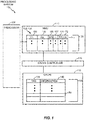
- cache 110 is shown in FIG. 1 as a direct mapped cache, for convenience of explanation.
- cache 110 is shown to comprise one or more cache lines or cache entries 130, wherein each cache entry 130 comprises tag 135 and information 145.
- Tag 135 is a field formed by a selected subset of bits of addresses (more specifically, physical addresses) at which corresponding information 145 is stored.
- Cache 110 can be indexed based on tags 135.
- cache controller 175 may compare tag 135 of all cache entries 130 with corresponding bits of an address for which a cache access is desired (e.g., an address corresponding to a memory access request made by processor 105) and if there is a match with tag 135 of any cache entry 130, then there is a cache-hit and the cache entry whose tag 135 matches the address for the desired cache access is referred to as the hitting cache entry. If tags 135 of none of cache entries 130 match the address for the desired cache access, then there is a cache-miss.
- a new cache entry may be created in cache 110 (which may involve any manner of creating a new cache entry or replacing an existing one by cache controller 175, using techniques such as a most recently used (MRU), least recently used (LRU), etc., as known in the art).
- MRU most recently used
- LRU least recently used
- Prior information corresponding to the write-address may be brought into cache 110 from a backing storage location where the write-address is found, and information corresponding to the write operation may be written to the new cache entry and tagged based on the write-address (more specifically, the tag may be based on a physical address translation of the write-address if the write-address is specified as a virtual address).
- servicing the write-miss involves writing the information to the backing storage location where the write-address is found, without creating a new cache entry and without writing the information in the new cache entry in cache 110.
- the various permissions which may be used in determining the write-allocation policy may be provided by MMU 115 in some aspects.
- MMU 115 may be generally configured to manage access to cache 110 (e.g., in cooperation with cache controller 175), as well as access to other memories not explicitly shown.
- MMU 115 may comprise TLB 125 configured for address translation.
- Processor 105 may use virtual addresses in its operation, whereas cache 110, as well as other memories in processing system 100, may be indexed and accessed using physical addresses.
- TLB 125 may store a relatively small number of virtual-to-physical address translations which are likely to be used by processor 105, for example, to enable a fast address translation for memory access requests generated by processor 105.
- TLB 125 may be populated according to known techniques to store address translations which have a high likelihood of future use by processor 105 (e.g., frequently used address translations, recently used address translations, etc.). If TLB 125 does not contain a translation for a particular memory access request (i.e., there is a "TLB-miss"), then a more time-consuming process of performing page table walks to determine the desired address translation may be undertaken by MMU 115, but techniques for populating TLB 125 and/or handling a TLB-miss are beyond the scope of this disclosure.
- TLB 125 does include one or more TLB entries, also referred to as page table entries (PTEs), collectively designated by the reference numeral 120 in FIG. 1 . Further details of an example PTE 155 of PTEs 120 are illustrated. PTE 155 is shown to comprise virtual address (VA) 160, a corresponding translation to physical address (PA) 140. Additionally, according to the invention TLB 125 does also include permission bits, such as supervisor write permission (SW) 165, user write permission (UW) 167, supervisor execute permission (SX) 170, and user execute permission (UX) 172.
- SW supervisor write permission
- UW supervisor write permission
- SX supervisor execute permission
- UX user execute permission
- SW 165 and UW 167 are write (W) permissions associated with supervisor (S) and user (U) privilege levels for PA 140 (which may be a write-address, e.g., in a main memory), or more generally, for a memory page which comprises physical address 140.
- SX 170 and UX 172 are execute (X) permissions associated with supervisor (S) and user (U) privilege levels for PA 140.
- PTE 155 can also include one or more read permission bits corresponding to physical addresses or memory pages, but these are not specifically shown or described because read accesses are not particularly discussed in this disclosure, as previously stated.
- the memory access request may be a write-request to write information (e.g., write-data which comprises an instruction) to a write-address. Since processor 105 makes the write-request, the write-address may be expressed as a virtual address in the write-request. Assuming a TLB-hit for PTE 155 in TLB 125 for the write-request, PTE 155 comprises VA 160 and a corresponding translation to PA 140 for the write-address.
- PTE 155 also comprises SW 165 and UW 167 corresponding to PA 140.
- the privilege level (user/supervisor) of the producing agent which generated the write-request may be known when the write-request is generated. Therefore, the corresponding write permission, SW 165 or UW 167, is checked based on whether the privilege level of the producer is supervisor or user, respectively. If the corresponding write permission is not asserted (or de-asserted) then write permission for the write-request may not be available, and cache controller 175, for example, may not permit access of cache 110 for the write-request; the write-request may be terminated and/or an exception/error flag may be generated and handled in ways which are beyond the scope of this disclosure and therefore cache access may be avoided.
- the write-request may be processed as follows.
- Cache controller 175, for example, may consult or probe cache 110, using the write-address or PA 140. If any of cache entries 130 has tag 135 which matches corresponding bits of PA 140, then there is a cache-hit or write-hit and cache controller 175 can write the write-data to the hitting cache entry. If, on the other hand, none of tags 135 matched corresponding bits of PA 140, then there is a write-miss.
- Processing the write-miss is based on SX 170 and UX 172.
- the potential consuming agent for the write-data may not be known. Therefore, one or more of the execute permissions SX 170 and UX 172 associated with the write-address may be considered, since the privilege level of a potential consuming agent which might execute the write-address may be one of a supervisor privilege or user privilege.
- One or more combinations of SX 170 and UX 172 will be described in detail in the following sections, in making the determination of whether to write-allocate or write-no-allocate in cache 110 while servicing the write-miss.
- the write-miss is determined to be serviced as a write-allocate
- one or more backing storage locations e.g., L2 cache, L3 cache, main memory, etc.
- the first backing storage location which comprises the write-address or PA 140 is accessed.
- the prior information stored in the backing storage location at PA 140 is read out and cache controller 175 may create new cache entry 150 in cache 110.
- Cache controller 175 may write the write-data to information 145 of the new cache entry 150, and set tag 135 of the new cache entry 150 based on bits of PA 140.
- the write-miss is determined to be serviced as a write-no-allocate
- one or more backing storage locations e.g., L2 cache, L3 cache, main memory, etc.
- the first backing storage location which comprises PA 140 is accessed.
- the prior information stored in the backing storage location at PA 140 overwritten with the first data, but a new cache entry 150 is not created in cache 110.
- SX 170 and UX 172 upon which write-allocate or write-no-allocate determinations may be based, will now be described in greater detail.
- the corresponding write permission (SW 165 or UW 167) based on the privilege level of the producing agent is asserted.
- the producing agent's privilege level may be known, which means that the producing agent's execute permission associated with the known privilege level may also be known, however, the privilege level or execute permission associated with a potential consuming agent may not be known, but may be assumed to be one of SX 170 or UX 172.
- the write-miss may be serviced as a write-allocate only if SX 170 is asserted, i.e., only if there is execute permissions for supervisor privilege.
- the value of UX 172 may not be considered.
- the write-miss may be serviced as a write-allocate only if UX 172 is asserted, i.e., only if there is execute permissions for user privilege.
- the value of SX 170 may not be considered.
- the write-miss may be serviced as a write-allocate only if at least one of SX 170 or UX 172 is asserted, i.e., if there is execute permissions for supervisor privilege and/or user privilege.
- the write-miss may be serviced as a write-allocate only if the execute permission for the producing agent's privilege level is asserted (i.e., only if SX 170 or UX 172 is asserted based on whether the producing agent is operated in a supervisor privilege level or a user privilege level, respectively).
- the producing agent may be operated under a supervisor privilege to produce instructions or code to be consumed or executed by potential consuming agents with supervisor privilege only (but not by potential consuming agents with user privilege); or the producing agent may be operated under a user privilege to produce instructions or code to be consumed or executed by potential consuming agents operated under user privilege only (but not by potential consuming agents with supervisor privilege).
- the execute permission associated with a privilege level which is not the privilege level of the producing agent is not considered, but only the execute permission associated with the privilege level of the producing agent is considered.
- the write-miss may be serviced as a write-allocate only if the execute permission for the privilege level which is not the producing agent's privilege level is asserted (i.e., only if SX 170 or UX 172 is asserted based on whether the producing agent is operated in a user privilege level or a supervisor privilege level, respectively).
- the execute permission associated with a privilege level which is not the privilege level of the producing agent is considered, but the execute permission associated with the privilege level of the producing agent is not considered.
- cache controller 175 may override an existing write-allocation policy or a default write-allocation policy. For example, a default write-no-allocate policy can be overridden to enforce write-allocate, or a default write-allocate policy can be overridden to enforce write-no-allocate for a write-miss based on one or more execute permissions associated with the write-address.
- exemplary aspects of this disclosure can include any logic configured to determine one or more execute permissions associated with a write-address of a write-request to cache 110.
- the logic can comprise MMU 115 as described above.
- the logic configured to determine the one or more execute permissions need not include an MMU such as MMU 115.
- the logic can include any other entity or unit, such as cache controller 175, used for controlling access to cache 110, wherein information regarding write and execute permissions for the various privilege levels (e.g., user/supervisor) may be provided to such logic.
- address translation may not be performed for cache access, and so a TLB such as TLB 125 may be avoided; for example, if cache 110 is virtually tagged (i.e., using virtual address 160) supplied by memory access requests generated by processor 105, cache 110 may be accessed without a TLB and so the logic can include cache controller 175 configured to determine information pertaining to the above-described write and execute permissions for the various privilege levels (e.g., user/supervisor) which are possible.
- the generated memory access requests may already be physical addresses and cache 110 may be a physically tagged cache (as shown in FIG. 1 ), and so the logic can comprise cache controller 175 configured to determine the above-described write and execute permissions.
- Other alternatives for cache access, cache configuration, and suitable logic configured to determine write and execute permissions for an intended write address to the cache are also possible, as will be recognized by one of skill in the art.
- FIG. 2 illustrates method 200 of managing a cache, such as cache 110 configured as a unified cache, to store data as well as instructions.
- Block 205 of method 200 comprises determining one or more execute permissions associated with a write-address of a write-request to the cache.
- the one or more execute permissions associated with the write-address e.g., physical address 140
- the one or more execute permissions can correspond to the execute permissions for a producing agent which generated the write-request and an execute permission of a potential consuming agent which may execute the write-address.
- the producing agent and the consuming agent may be processes of processor 105 configured to access cache 110.
- the one or more execute permissions associated with the write-address may be retrieved from a page table entry (e.g., PTE 155) of a translation lookaside buffer (e.g., TLB 125) comprising an address translation (e.g., physical address 140) for the write-address and the one or more execute permissions (e.g., SX 170, UX 172) associated with the write-address.
- method 200 can include determining if there is a write-miss in the cache for the write-request (e.g., cache controller 175 may probe cache 110 using physical address 140). If there is a write-miss, cache controller 175, for example, may determine whether to implement a write-allocate policy or a write-no-allocate policy for servicing the write-miss, based on the one or more execute permissions.
- Blocks 205-210 are not limiting of the examples. As such, Blocks 205-215 can be combined and/or their order can be rearranged, as practicable.
- FIG. 3 is a block diagram of a particular illustrative aspect of a computing device 300, according to exemplary aspects.
- Computing device 300 may be configured to perform method 200 of FIG. 2 in exemplary aspects.
- computing device 300 includes processor 105.
- MMU 115 comprising TLB 125, cache controller 175, and cache 110 as described with reference to FIG. 1 have been shown, although the additional details of these components that are shown in FIG. 1 are omitted from FIG. 3 for the sake of clarity.
- aspects such as MMU 115 comprising TLB 125, cache controller 175, and cache 110 have been shown as components which are outside processor 105 in FIGS. 1 and 3 , this arrangement is purely for the sake of illustration, and not to be construed as a limitation.
- components such as MMU 115 comprising TLB 125, cache controller 175, or cache 110 may be configured within the block illustrated as processor 105. Skilled persons will recognize various other arrangements and configurations that are possible for processor 105, MMU 115 comprising TLB 125, cache controller 175, and cache 110 according to aspects of this disclosure.
- FIG. 3 also shows memory 305, which may be a backing storage location for cache 110, such as main memory. Although not shown, one or more other caches or other memory structures may also be included in computing device 300. Also shown in FIG. 3 are display 315 and display controller 310, with display controller 310 coupled to processor 105 and to display 315.
- FIG. 3 may include some optional blocks showed with dashed lines.
- computing device 300 may optionally include coder/decoder (CODEC) 320 (e.g., an audio and/or voice CODEC) coupled to processor 105; speaker 330 and microphone 335 coupled to CODEC 320; and wireless controller 325 (which may include a modem) coupled to wireless antenna 340 and to processor 105.
- CDEC coder/decoder
- wireless controller 325 which may include a modem
- processor 105, display controller 310, memory 305, CODEC 320, and wireless controller 325 can be included in a system-in-package or a system-on-chip device 345; and display 315, input device 350, speaker 330, microphone 335, wireless antenna 340, and power supply 355 may be external to system-on-chip device 345, and may be coupled to a component of system-on-chip device 345, such as an interface or a controller.
- FIG. 3 generally depicts a computing device
- processor 105 and memory 305 may be integrated into a set top box, a music player, a video player, an entertainment unit, a navigation device, a personal digital assistant (PDA), a fixed location data unit, a server, a computer, a laptop, a tablet, a communications device, and a mobile phone, or other electronic devices.
- PDA personal digital assistant
- at least one or more exemplary aspects of computing device 300 may be integrated in at least one semiconductor die.
- a software module may reside in RAM memory, flash memory, ROM memory, EPROM memory, EEPROM memory, registers, hard disk, a removable disk, a CD-ROM, or any other form of storage medium known in the art.
- An exemplary storage medium is coupled to the processor such that the processor can read information from, and write information to, the storage medium. In the alternative, the storage medium may be integral to the processor.
- an aspect of the invention can include computer readable media embodying a method for managing a cache. Accordingly, the invention is not limited to illustrated examples and any means for performing the functionality described herein are included in embodiments of the invention.
Landscapes
- Engineering & Computer Science (AREA)
- Theoretical Computer Science (AREA)
- Physics & Mathematics (AREA)
- General Engineering & Computer Science (AREA)
- General Physics & Mathematics (AREA)
- Memory System Of A Hierarchy Structure (AREA)
- Storage Device Security (AREA)
Applications Claiming Priority (2)
| Application Number | Priority Date | Filing Date | Title |
|---|---|---|---|
| US15/057,121 US20170255569A1 (en) | 2016-03-01 | 2016-03-01 | Write-allocation for a cache based on execute permissions |
| PCT/US2017/016971 WO2017151280A1 (en) | 2016-03-01 | 2017-02-08 | Write-allocation for a cache based on execute permissions |
Publications (2)
| Publication Number | Publication Date |
|---|---|
| EP3423946A1 EP3423946A1 (en) | 2019-01-09 |
| EP3423946B1 true EP3423946B1 (en) | 2021-12-15 |
Family
ID=58018350
Family Applications (1)
| Application Number | Title | Priority Date | Filing Date |
|---|---|---|---|
| EP17705003.6A Active EP3423946B1 (en) | 2016-03-01 | 2017-02-08 | Write-allocation for a cache based on execute permissions |
Country Status (11)
| Country | Link |
|---|---|
| US (1) | US20170255569A1 (pt) |
| EP (1) | EP3423946B1 (pt) |
| JP (1) | JP6960933B2 (pt) |
| KR (1) | KR20180117629A (pt) |
| CN (1) | CN108604210B (pt) |
| BR (1) | BR112018067341A2 (pt) |
| ES (1) | ES2903162T3 (pt) |
| HK (1) | HK1254828A1 (pt) |
| SG (1) | SG11201806067SA (pt) |
| TW (1) | TW201734807A (pt) |
| WO (1) | WO2017151280A1 (pt) |
Families Citing this family (8)
| Publication number | Priority date | Publication date | Assignee | Title |
|---|---|---|---|---|
| US10114768B2 (en) * | 2016-08-29 | 2018-10-30 | Intel Corporation | Enhance memory access permission based on per-page current privilege level |
| US10713177B2 (en) | 2016-09-09 | 2020-07-14 | Intel Corporation | Defining virtualized page attributes based on guest page attributes |
| US11010309B2 (en) * | 2018-05-18 | 2021-05-18 | Intel Corporation | Computer system and method for executing one or more software applications, host computer device and method for a host computer device, memory device and method for a memory device and non-transitory computer readable medium |
| CN111124267B (zh) * | 2018-10-31 | 2023-10-31 | 伊姆西Ip控股有限责任公司 | 数据写入的方法、设备和计算机程序产品 |
| CN112559389A (zh) * | 2019-09-25 | 2021-03-26 | 阿里巴巴集团控股有限公司 | 存储控制装置、处理装置、计算机系统和存储控制方法 |
| CN114616552A (zh) * | 2019-11-29 | 2022-06-10 | 华为技术有限公司 | 缓存存储器和分配写操作的方法 |
| CN111831587A (zh) * | 2020-04-17 | 2020-10-27 | 北京奕斯伟计算技术有限公司 | 数据写入方法、装置和电子设备 |
| US20230418753A1 (en) * | 2022-06-28 | 2023-12-28 | Advanced Micro Devices, Inc. | Allocation control for cache |
Citations (5)
| Publication number | Priority date | Publication date | Assignee | Title |
|---|---|---|---|---|
| US5606687A (en) * | 1993-10-07 | 1997-02-25 | Sun Microsystems, Inc. | Method and apparatus for optimizing supervisor mode store operations in a data cache |
| US5623619A (en) * | 1993-10-29 | 1997-04-22 | Advanced Micro Devices, Inc. | Linearly addressable microprocessor cache |
| EP1304620A1 (en) * | 2001-10-17 | 2003-04-23 | Texas Instruments Incorporated | Cache with selective write allocation |
| US20070094475A1 (en) * | 2005-10-20 | 2007-04-26 | Bridges Jeffrey T | Caching memory attribute indicators with cached memory data field |
| GB2526849A (en) * | 2014-06-05 | 2015-12-09 | Advanced Risc Mach Ltd | Dynamic cache allocation policy adaptation in a data processing apparatus |
Family Cites Families (18)
| Publication number | Priority date | Publication date | Assignee | Title |
|---|---|---|---|---|
| US6119151A (en) * | 1994-03-07 | 2000-09-12 | International Business Machines Corp. | System and method for efficient cache management in a distributed file system |
| US6263407B1 (en) * | 1998-02-17 | 2001-07-17 | International Business Machines Corporation | Cache coherency protocol including a hovering (H) state having a precise mode and an imprecise mode |
| JP2000215102A (ja) * | 1998-09-01 | 2000-08-04 | Texas Instr Inc <Ti> | プロセッサ用の進歩したメモリ階層構造 |
| US6412043B1 (en) * | 1999-10-01 | 2002-06-25 | Hitachi, Ltd. | Microprocessor having improved memory management unit and cache memory |
| JP2003044358A (ja) * | 2001-07-31 | 2003-02-14 | Mitsubishi Electric Corp | キャッシュメモリ制御装置 |
| US6990502B2 (en) * | 2003-02-26 | 2006-01-24 | Microsoft Corporation | Reviewing cached user-group information in connection with issuing a digital rights management (DRM) license for content |
| US7437510B2 (en) * | 2005-09-30 | 2008-10-14 | Intel Corporation | Instruction-assisted cache management for efficient use of cache and memory |
| US20070079070A1 (en) * | 2005-09-30 | 2007-04-05 | Arm Limited | Cache controller |
| US8606998B2 (en) * | 2006-08-24 | 2013-12-10 | Advanced Micro Devices, Inc. | System and method for instruction-based cache allocation policies |
| US8275971B2 (en) * | 2008-08-27 | 2012-09-25 | International Business Machines Corporation | Method and apparatus for managing software controlled cache of translating the physical memory access of a virtual machine between different levels of translation entities |
| US8621184B1 (en) * | 2008-10-31 | 2013-12-31 | Netapp, Inc. | Effective scheduling of producer-consumer processes in a multi-processor system |
| US8621149B2 (en) * | 2009-12-23 | 2013-12-31 | Intel Corporation | Controlling access to a cache memory using privilege level information |
| US8504777B2 (en) * | 2010-09-21 | 2013-08-06 | Freescale Semiconductor, Inc. | Data processor for processing decorated instructions with cache bypass |
| US20130179642A1 (en) * | 2012-01-10 | 2013-07-11 | Qualcomm Incorporated | Non-Allocating Memory Access with Physical Address |
| US9158685B2 (en) * | 2012-09-11 | 2015-10-13 | Apple Inc. | System cache with cache hint control |
| US8819342B2 (en) * | 2012-09-26 | 2014-08-26 | Qualcomm Incorporated | Methods and apparatus for managing page crossing instructions with different cacheability |
| US9335943B2 (en) * | 2014-06-30 | 2016-05-10 | Intel Corporation | Method and apparatus for fine grain memory protection |
| US9767040B2 (en) * | 2015-08-31 | 2017-09-19 | Salesforce.Com, Inc. | System and method for generating and storing real-time analytics metric data using an in memory buffer service consumer framework |
-
2016
- 2016-03-01 US US15/057,121 patent/US20170255569A1/en not_active Abandoned
-
2017
- 2017-02-08 BR BR112018067341A patent/BR112018067341A2/pt unknown
- 2017-02-08 ES ES17705003T patent/ES2903162T3/es active Active
- 2017-02-08 JP JP2018545297A patent/JP6960933B2/ja active Active
- 2017-02-08 WO PCT/US2017/016971 patent/WO2017151280A1/en active Application Filing
- 2017-02-08 KR KR1020187024970A patent/KR20180117629A/ko unknown
- 2017-02-08 SG SG11201806067SA patent/SG11201806067SA/en unknown
- 2017-02-08 EP EP17705003.6A patent/EP3423946B1/en active Active
- 2017-02-08 CN CN201780010875.1A patent/CN108604210B/zh active Active
- 2017-02-24 TW TW106106528A patent/TW201734807A/zh unknown
-
2018
- 2018-10-31 HK HK18113920.8A patent/HK1254828A1/zh unknown
Patent Citations (5)
| Publication number | Priority date | Publication date | Assignee | Title |
|---|---|---|---|---|
| US5606687A (en) * | 1993-10-07 | 1997-02-25 | Sun Microsystems, Inc. | Method and apparatus for optimizing supervisor mode store operations in a data cache |
| US5623619A (en) * | 1993-10-29 | 1997-04-22 | Advanced Micro Devices, Inc. | Linearly addressable microprocessor cache |
| EP1304620A1 (en) * | 2001-10-17 | 2003-04-23 | Texas Instruments Incorporated | Cache with selective write allocation |
| US20070094475A1 (en) * | 2005-10-20 | 2007-04-26 | Bridges Jeffrey T | Caching memory attribute indicators with cached memory data field |
| GB2526849A (en) * | 2014-06-05 | 2015-12-09 | Advanced Risc Mach Ltd | Dynamic cache allocation policy adaptation in a data processing apparatus |
Also Published As
| Publication number | Publication date |
|---|---|
| KR20180117629A (ko) | 2018-10-29 |
| WO2017151280A1 (en) | 2017-09-08 |
| JP2019511045A (ja) | 2019-04-18 |
| US20170255569A1 (en) | 2017-09-07 |
| SG11201806067SA (en) | 2018-09-27 |
| CN108604210A (zh) | 2018-09-28 |
| ES2903162T3 (es) | 2022-03-31 |
| HK1254828A1 (zh) | 2019-07-26 |
| BR112018067341A2 (pt) | 2019-01-08 |
| JP6960933B2 (ja) | 2021-11-05 |
| EP3423946A1 (en) | 2019-01-09 |
| TW201734807A (zh) | 2017-10-01 |
| CN108604210B (zh) | 2022-08-19 |
Similar Documents
| Publication | Publication Date | Title |
|---|---|---|
| EP3423946B1 (en) | Write-allocation for a cache based on execute permissions | |
| KR102448124B1 (ko) | 가상 주소들을 사용하여 액세스된 캐시 | |
| US10474584B2 (en) | Storing cache metadata separately from integrated circuit containing cache controller | |
| US9218286B2 (en) | System cache with partial write valid states | |
| US7284112B2 (en) | Multiple page size address translation incorporating page size prediction | |
| US8397049B2 (en) | TLB prefetching | |
| US9201796B2 (en) | System cache with speculative read engine | |
| US9158685B2 (en) | System cache with cache hint control | |
| US9418011B2 (en) | Region based technique for accurately predicting memory accesses | |
| US20130179642A1 (en) | Non-Allocating Memory Access with Physical Address | |
| US10083126B2 (en) | Apparatus and method for avoiding conflicting entries in a storage structure | |
| US9043554B2 (en) | Cache policies for uncacheable memory requests | |
| US20130304994A1 (en) | Per Thread Cacheline Allocation Mechanism in Shared Partitioned Caches in Multi-Threaded Processors | |
| US20140089600A1 (en) | System cache with data pending state | |
| US9311251B2 (en) | System cache with sticky allocation | |
| US8886886B2 (en) | System cache with sticky removal engine | |
| US11036639B2 (en) | Cache apparatus and method that facilitates a reduction in energy consumption through use of first and second data arrays | |
| US20230100230A1 (en) | Using request class and reuse recording in one cache for insertion policies of another cache | |
| US20150286270A1 (en) | Method and system for reducing power consumption while improving efficiency for a memory management unit of a portable computing device |
Legal Events
| Date | Code | Title | Description |
|---|---|---|---|
| STAA | Information on the status of an ep patent application or granted ep patent |
Free format text: STATUS: UNKNOWN |
|
| STAA | Information on the status of an ep patent application or granted ep patent |
Free format text: STATUS: THE INTERNATIONAL PUBLICATION HAS BEEN MADE |
|
| PUAI | Public reference made under article 153(3) epc to a published international application that has entered the european phase |
Free format text: ORIGINAL CODE: 0009012 |
|
| STAA | Information on the status of an ep patent application or granted ep patent |
Free format text: STATUS: REQUEST FOR EXAMINATION WAS MADE |
|
| 17P | Request for examination filed |
Effective date: 20180713 |
|
| AK | Designated contracting states |
Kind code of ref document: A1 Designated state(s): AL AT BE BG CH CY CZ DE DK EE ES FI FR GB GR HR HU IE IS IT LI LT LU LV MC MK MT NL NO PL PT RO RS SE SI SK SM TR |
|
| AX | Request for extension of the european patent |
Extension state: BA ME |
|
| DAV | Request for validation of the european patent (deleted) | ||
| DAX | Request for extension of the european patent (deleted) | ||
| STAA | Information on the status of an ep patent application or granted ep patent |
Free format text: STATUS: EXAMINATION IS IN PROGRESS |
|
| 17Q | First examination report despatched |
Effective date: 20190626 |
|
| STAA | Information on the status of an ep patent application or granted ep patent |
Free format text: STATUS: EXAMINATION IS IN PROGRESS |
|
| GRAP | Despatch of communication of intention to grant a patent |
Free format text: ORIGINAL CODE: EPIDOSNIGR1 |
|
| STAA | Information on the status of an ep patent application or granted ep patent |
Free format text: STATUS: GRANT OF PATENT IS INTENDED |
|
| INTG | Intention to grant announced |
Effective date: 20210709 |
|
| GRAS | Grant fee paid |
Free format text: ORIGINAL CODE: EPIDOSNIGR3 |
|
| GRAA | (expected) grant |
Free format text: ORIGINAL CODE: 0009210 |
|
| STAA | Information on the status of an ep patent application or granted ep patent |
Free format text: STATUS: THE PATENT HAS BEEN GRANTED |
|
| AK | Designated contracting states |
Kind code of ref document: B1 Designated state(s): AL AT BE BG CH CY CZ DE DK EE ES FI FR GB GR HR HU IE IS IT LI LT LU LV MC MK MT NL NO PL PT RO RS SE SI SK SM TR |
|
| REG | Reference to a national code |
Ref country code: GB Ref legal event code: FG4D Ref country code: CH Ref legal event code: EP |
|
| REG | Reference to a national code |
Ref country code: IE Ref legal event code: FG4D Ref country code: DE Ref legal event code: R096 Ref document number: 602017050891 Country of ref document: DE |
|
| REG | Reference to a national code |
Ref country code: AT Ref legal event code: REF Ref document number: 1455997 Country of ref document: AT Kind code of ref document: T Effective date: 20220115 |
|
| REG | Reference to a national code |
Ref country code: NL Ref legal event code: FP |
|
| REG | Reference to a national code |
Ref country code: SE Ref legal event code: TRGR |
|
| REG | Reference to a national code |
Ref country code: NO Ref legal event code: T2 Effective date: 20211215 |
|
| REG | Reference to a national code |
Ref country code: ES Ref legal event code: FG2A Ref document number: 2903162 Country of ref document: ES Kind code of ref document: T3 Effective date: 20220331 |
|
| REG | Reference to a national code |
Ref country code: LT Ref legal event code: MG9D |
|
| PG25 | Lapsed in a contracting state [announced via postgrant information from national office to epo] |
Ref country code: RS Free format text: LAPSE BECAUSE OF FAILURE TO SUBMIT A TRANSLATION OF THE DESCRIPTION OR TO PAY THE FEE WITHIN THE PRESCRIBED TIME-LIMIT Effective date: 20211215 Ref country code: LT Free format text: LAPSE BECAUSE OF FAILURE TO SUBMIT A TRANSLATION OF THE DESCRIPTION OR TO PAY THE FEE WITHIN THE PRESCRIBED TIME-LIMIT Effective date: 20211215 Ref country code: FI Free format text: LAPSE BECAUSE OF FAILURE TO SUBMIT A TRANSLATION OF THE DESCRIPTION OR TO PAY THE FEE WITHIN THE PRESCRIBED TIME-LIMIT Effective date: 20211215 Ref country code: BG Free format text: LAPSE BECAUSE OF FAILURE TO SUBMIT A TRANSLATION OF THE DESCRIPTION OR TO PAY THE FEE WITHIN THE PRESCRIBED TIME-LIMIT Effective date: 20220315 |
|
| REG | Reference to a national code |
Ref country code: AT Ref legal event code: MK05 Ref document number: 1455997 Country of ref document: AT Kind code of ref document: T Effective date: 20211215 |
|
| PG25 | Lapsed in a contracting state [announced via postgrant information from national office to epo] |
Ref country code: LV Free format text: LAPSE BECAUSE OF FAILURE TO SUBMIT A TRANSLATION OF THE DESCRIPTION OR TO PAY THE FEE WITHIN THE PRESCRIBED TIME-LIMIT Effective date: 20211215 Ref country code: HR Free format text: LAPSE BECAUSE OF FAILURE TO SUBMIT A TRANSLATION OF THE DESCRIPTION OR TO PAY THE FEE WITHIN THE PRESCRIBED TIME-LIMIT Effective date: 20211215 Ref country code: GR Free format text: LAPSE BECAUSE OF FAILURE TO SUBMIT A TRANSLATION OF THE DESCRIPTION OR TO PAY THE FEE WITHIN THE PRESCRIBED TIME-LIMIT Effective date: 20220316 |
|
| PG25 | Lapsed in a contracting state [announced via postgrant information from national office to epo] |
Ref country code: SM Free format text: LAPSE BECAUSE OF FAILURE TO SUBMIT A TRANSLATION OF THE DESCRIPTION OR TO PAY THE FEE WITHIN THE PRESCRIBED TIME-LIMIT Effective date: 20211215 Ref country code: SK Free format text: LAPSE BECAUSE OF FAILURE TO SUBMIT A TRANSLATION OF THE DESCRIPTION OR TO PAY THE FEE WITHIN THE PRESCRIBED TIME-LIMIT Effective date: 20211215 Ref country code: RO Free format text: LAPSE BECAUSE OF FAILURE TO SUBMIT A TRANSLATION OF THE DESCRIPTION OR TO PAY THE FEE WITHIN THE PRESCRIBED TIME-LIMIT Effective date: 20211215 Ref country code: PT Free format text: LAPSE BECAUSE OF FAILURE TO SUBMIT A TRANSLATION OF THE DESCRIPTION OR TO PAY THE FEE WITHIN THE PRESCRIBED TIME-LIMIT Effective date: 20220418 Ref country code: EE Free format text: LAPSE BECAUSE OF FAILURE TO SUBMIT A TRANSLATION OF THE DESCRIPTION OR TO PAY THE FEE WITHIN THE PRESCRIBED TIME-LIMIT Effective date: 20211215 Ref country code: CZ Free format text: LAPSE BECAUSE OF FAILURE TO SUBMIT A TRANSLATION OF THE DESCRIPTION OR TO PAY THE FEE WITHIN THE PRESCRIBED TIME-LIMIT Effective date: 20211215 |
|
| PG25 | Lapsed in a contracting state [announced via postgrant information from national office to epo] |
Ref country code: PL Free format text: LAPSE BECAUSE OF FAILURE TO SUBMIT A TRANSLATION OF THE DESCRIPTION OR TO PAY THE FEE WITHIN THE PRESCRIBED TIME-LIMIT Effective date: 20211215 Ref country code: AT Free format text: LAPSE BECAUSE OF FAILURE TO SUBMIT A TRANSLATION OF THE DESCRIPTION OR TO PAY THE FEE WITHIN THE PRESCRIBED TIME-LIMIT Effective date: 20211215 |
|
| REG | Reference to a national code |
Ref country code: DE Ref legal event code: R097 Ref document number: 602017050891 Country of ref document: DE |
|
| PG25 | Lapsed in a contracting state [announced via postgrant information from national office to epo] |
Ref country code: MC Free format text: LAPSE BECAUSE OF FAILURE TO SUBMIT A TRANSLATION OF THE DESCRIPTION OR TO PAY THE FEE WITHIN THE PRESCRIBED TIME-LIMIT Effective date: 20211215 Ref country code: IS Free format text: LAPSE BECAUSE OF FAILURE TO SUBMIT A TRANSLATION OF THE DESCRIPTION OR TO PAY THE FEE WITHIN THE PRESCRIBED TIME-LIMIT Effective date: 20220415 |
|
| PLBE | No opposition filed within time limit |
Free format text: ORIGINAL CODE: 0009261 |
|
| STAA | Information on the status of an ep patent application or granted ep patent |
Free format text: STATUS: NO OPPOSITION FILED WITHIN TIME LIMIT |
|
| REG | Reference to a national code |
Ref country code: BE Ref legal event code: MM Effective date: 20220228 |
|
| PG25 | Lapsed in a contracting state [announced via postgrant information from national office to epo] |
Ref country code: LU Free format text: LAPSE BECAUSE OF NON-PAYMENT OF DUE FEES Effective date: 20220208 Ref country code: DK Free format text: LAPSE BECAUSE OF FAILURE TO SUBMIT A TRANSLATION OF THE DESCRIPTION OR TO PAY THE FEE WITHIN THE PRESCRIBED TIME-LIMIT Effective date: 20211215 Ref country code: AL Free format text: LAPSE BECAUSE OF FAILURE TO SUBMIT A TRANSLATION OF THE DESCRIPTION OR TO PAY THE FEE WITHIN THE PRESCRIBED TIME-LIMIT Effective date: 20211215 |
|
| 26N | No opposition filed |
Effective date: 20220916 |
|
| PG25 | Lapsed in a contracting state [announced via postgrant information from national office to epo] |
Ref country code: SI Free format text: LAPSE BECAUSE OF FAILURE TO SUBMIT A TRANSLATION OF THE DESCRIPTION OR TO PAY THE FEE WITHIN THE PRESCRIBED TIME-LIMIT Effective date: 20211215 |
|
| PG25 | Lapsed in a contracting state [announced via postgrant information from national office to epo] |
Ref country code: IE Free format text: LAPSE BECAUSE OF NON-PAYMENT OF DUE FEES Effective date: 20220208 |
|
| PG25 | Lapsed in a contracting state [announced via postgrant information from national office to epo] |
Ref country code: BE Free format text: LAPSE BECAUSE OF NON-PAYMENT OF DUE FEES Effective date: 20220228 |
|
| PGFP | Annual fee paid to national office [announced via postgrant information from national office to epo] |
Ref country code: NO Payment date: 20230127 Year of fee payment: 7 Ref country code: FR Payment date: 20230109 Year of fee payment: 7 |
|
| PG25 | Lapsed in a contracting state [announced via postgrant information from national office to epo] |
Ref country code: IT Free format text: LAPSE BECAUSE OF FAILURE TO SUBMIT A TRANSLATION OF THE DESCRIPTION OR TO PAY THE FEE WITHIN THE PRESCRIBED TIME-LIMIT Effective date: 20211215 |
|
| PGFP | Annual fee paid to national office [announced via postgrant information from national office to epo] |
Ref country code: SE Payment date: 20230208 Year of fee payment: 7 |
|
| PGFP | Annual fee paid to national office [announced via postgrant information from national office to epo] |
Ref country code: NL Payment date: 20240111 Year of fee payment: 8 |
|
| PG25 | Lapsed in a contracting state [announced via postgrant information from national office to epo] |
Ref country code: HU Free format text: LAPSE BECAUSE OF FAILURE TO SUBMIT A TRANSLATION OF THE DESCRIPTION OR TO PAY THE FEE WITHIN THE PRESCRIBED TIME-LIMIT; INVALID AB INITIO Effective date: 20170208 |
|
| PGFP | Annual fee paid to national office [announced via postgrant information from national office to epo] |
Ref country code: ES Payment date: 20240306 Year of fee payment: 8 |
|
| PG25 | Lapsed in a contracting state [announced via postgrant information from national office to epo] |
Ref country code: MK Free format text: LAPSE BECAUSE OF FAILURE TO SUBMIT A TRANSLATION OF THE DESCRIPTION OR TO PAY THE FEE WITHIN THE PRESCRIBED TIME-LIMIT Effective date: 20211215 Ref country code: CY Free format text: LAPSE BECAUSE OF FAILURE TO SUBMIT A TRANSLATION OF THE DESCRIPTION OR TO PAY THE FEE WITHIN THE PRESCRIBED TIME-LIMIT Effective date: 20211215 |
|
| PGFP | Annual fee paid to national office [announced via postgrant information from national office to epo] |
Ref country code: DE Payment date: 20240109 Year of fee payment: 8 Ref country code: GB Payment date: 20240111 Year of fee payment: 8 Ref country code: CH Payment date: 20240301 Year of fee payment: 8 |