EP3423858B1 - 3d imaging system and method - Google Patents
3d imaging system and method Download PDFInfo
- Publication number
- EP3423858B1 EP3423858B1 EP17760645.6A EP17760645A EP3423858B1 EP 3423858 B1 EP3423858 B1 EP 3423858B1 EP 17760645 A EP17760645 A EP 17760645A EP 3423858 B1 EP3423858 B1 EP 3423858B1
- Authority
- EP
- European Patent Office
- Prior art keywords
- elements
- pixel
- array
- optical
- pixels
- Prior art date
- Legal status (The legal status is an assumption and is not a legal conclusion. Google has not performed a legal analysis and makes no representation as to the accuracy of the status listed.)
- Active
Links
- 238000000034 method Methods 0.000 title claims description 63
- 238000003384 imaging method Methods 0.000 title claims description 35
- 230000010287 polarization Effects 0.000 claims description 74
- 230000003287 optical effect Effects 0.000 claims description 55
- 230000005540 biological transmission Effects 0.000 claims description 50
- 238000000576 coating method Methods 0.000 claims description 12
- 239000011248 coating agent Substances 0.000 claims description 5
- BJQHLKABXJIVAM-UHFFFAOYSA-N bis(2-ethylhexyl) phthalate Chemical compound CCCCC(CC)COC(=O)C1=CC=CC=C1C(=O)OCC(CC)CCCC BJQHLKABXJIVAM-UHFFFAOYSA-N 0.000 claims description 3
- 238000003491 array Methods 0.000 description 19
- 238000013461 design Methods 0.000 description 17
- 239000000463 material Substances 0.000 description 14
- 238000005286 illumination Methods 0.000 description 13
- 239000000758 substrate Substances 0.000 description 13
- 230000004044 response Effects 0.000 description 12
- 238000013459 approach Methods 0.000 description 10
- 230000000875 corresponding effect Effects 0.000 description 9
- 238000005259 measurement Methods 0.000 description 8
- 229910052751 metal Inorganic materials 0.000 description 8
- 239000002184 metal Substances 0.000 description 8
- 230000008859 change Effects 0.000 description 7
- 230000000694 effects Effects 0.000 description 7
- 238000000151 deposition Methods 0.000 description 6
- 238000010586 diagram Methods 0.000 description 6
- 238000004519 manufacturing process Methods 0.000 description 6
- 230000008569 process Effects 0.000 description 6
- 238000012545 processing Methods 0.000 description 6
- 238000000926 separation method Methods 0.000 description 6
- 229920002120 photoresistant polymer Polymers 0.000 description 5
- 230000004075 alteration Effects 0.000 description 4
- 229910052782 aluminium Inorganic materials 0.000 description 4
- XAGFODPZIPBFFR-UHFFFAOYSA-N aluminium Chemical compound [Al] XAGFODPZIPBFFR-UHFFFAOYSA-N 0.000 description 4
- 238000001465 metallisation Methods 0.000 description 4
- 229920000642 polymer Polymers 0.000 description 4
- 239000004065 semiconductor Substances 0.000 description 4
- 230000008021 deposition Effects 0.000 description 3
- 238000011161 development Methods 0.000 description 3
- 238000005530 etching Methods 0.000 description 3
- 239000004973 liquid crystal related substance Substances 0.000 description 3
- 238000002161 passivation Methods 0.000 description 3
- 238000000059 patterning Methods 0.000 description 3
- 206010003549 asthenia Diseases 0.000 description 2
- 230000001419 dependent effect Effects 0.000 description 2
- 238000005516 engineering process Methods 0.000 description 2
- 230000004907 flux Effects 0.000 description 2
- 239000011521 glass Substances 0.000 description 2
- 238000010606 normalization Methods 0.000 description 2
- 230000003595 spectral effect Effects 0.000 description 2
- 239000010409 thin film Substances 0.000 description 2
- 230000036962 time dependent Effects 0.000 description 2
- 239000012780 transparent material Substances 0.000 description 2
- 208000016258 weakness Diseases 0.000 description 2
- BQCADISMDOOEFD-UHFFFAOYSA-N Silver Chemical compound [Ag] BQCADISMDOOEFD-UHFFFAOYSA-N 0.000 description 1
- 239000011358 absorbing material Substances 0.000 description 1
- 239000006117 anti-reflective coating Substances 0.000 description 1
- 238000004364 calculation method Methods 0.000 description 1
- 238000012512 characterization method Methods 0.000 description 1
- 230000000295 complement effect Effects 0.000 description 1
- 230000002596 correlated effect Effects 0.000 description 1
- 230000002939 deleterious effect Effects 0.000 description 1
- 230000005684 electric field Effects 0.000 description 1
- 239000002305 electric material Substances 0.000 description 1
- 230000007613 environmental effect Effects 0.000 description 1
- 238000000605 extraction Methods 0.000 description 1
- 239000010408 film Substances 0.000 description 1
- 150000002222 fluorine compounds Chemical class 0.000 description 1
- PCHJSUWPFVWCPO-UHFFFAOYSA-N gold Chemical compound [Au] PCHJSUWPFVWCPO-UHFFFAOYSA-N 0.000 description 1
- 229910052737 gold Inorganic materials 0.000 description 1
- 239000010931 gold Substances 0.000 description 1
- 229910044991 metal oxide Inorganic materials 0.000 description 1
- 150000004706 metal oxides Chemical class 0.000 description 1
- 150000002739 metals Chemical class 0.000 description 1
- 238000002156 mixing Methods 0.000 description 1
- 239000000203 mixture Substances 0.000 description 1
- 238000012986 modification Methods 0.000 description 1
- 230000004048 modification Effects 0.000 description 1
- 239000002070 nanowire Substances 0.000 description 1
- 239000000382 optic material Substances 0.000 description 1
- 238000000711 polarimetry Methods 0.000 description 1
- 229910021420 polycrystalline silicon Inorganic materials 0.000 description 1
- 238000002310 reflectometry Methods 0.000 description 1
- 230000035945 sensitivity Effects 0.000 description 1
- 229910052709 silver Inorganic materials 0.000 description 1
- 239000004332 silver Substances 0.000 description 1
- 230000002123 temporal effect Effects 0.000 description 1
Images


Classifications
-
- G—PHYSICS
- G01—MEASURING; TESTING
- G01S—RADIO DIRECTION-FINDING; RADIO NAVIGATION; DETERMINING DISTANCE OR VELOCITY BY USE OF RADIO WAVES; LOCATING OR PRESENCE-DETECTING BY USE OF THE REFLECTION OR RERADIATION OF RADIO WAVES; ANALOGOUS ARRANGEMENTS USING OTHER WAVES
- G01S7/00—Details of systems according to groups G01S13/00, G01S15/00, G01S17/00
- G01S7/48—Details of systems according to groups G01S13/00, G01S15/00, G01S17/00 of systems according to group G01S17/00
- G01S7/481—Constructional features, e.g. arrangements of optical elements
- G01S7/4816—Constructional features, e.g. arrangements of optical elements of receivers alone
-
- G—PHYSICS
- G02—OPTICS
- G02B—OPTICAL ELEMENTS, SYSTEMS OR APPARATUS
- G02B30/00—Optical systems or apparatus for producing three-dimensional [3D] effects, e.g. stereoscopic images
- G02B30/20—Optical systems or apparatus for producing three-dimensional [3D] effects, e.g. stereoscopic images by providing first and second parallax images to an observer's left and right eyes
- G02B30/22—Optical systems or apparatus for producing three-dimensional [3D] effects, e.g. stereoscopic images by providing first and second parallax images to an observer's left and right eyes of the stereoscopic type
- G02B30/25—Optical systems or apparatus for producing three-dimensional [3D] effects, e.g. stereoscopic images by providing first and second parallax images to an observer's left and right eyes of the stereoscopic type using polarisation techniques
-
- G—PHYSICS
- G01—MEASURING; TESTING
- G01S—RADIO DIRECTION-FINDING; RADIO NAVIGATION; DETERMINING DISTANCE OR VELOCITY BY USE OF RADIO WAVES; LOCATING OR PRESENCE-DETECTING BY USE OF THE REFLECTION OR RERADIATION OF RADIO WAVES; ANALOGOUS ARRANGEMENTS USING OTHER WAVES
- G01S17/00—Systems using the reflection or reradiation of electromagnetic waves other than radio waves, e.g. lidar systems
- G01S17/88—Lidar systems specially adapted for specific applications
- G01S17/89—Lidar systems specially adapted for specific applications for mapping or imaging
- G01S17/894—3D imaging with simultaneous measurement of time-of-flight at a 2D array of receiver pixels, e.g. time-of-flight cameras or flash lidar
-
- G—PHYSICS
- G01—MEASURING; TESTING
- G01S—RADIO DIRECTION-FINDING; RADIO NAVIGATION; DETERMINING DISTANCE OR VELOCITY BY USE OF RADIO WAVES; LOCATING OR PRESENCE-DETECTING BY USE OF THE REFLECTION OR RERADIATION OF RADIO WAVES; ANALOGOUS ARRANGEMENTS USING OTHER WAVES
- G01S7/00—Details of systems according to groups G01S13/00, G01S15/00, G01S17/00
- G01S7/48—Details of systems according to groups G01S13/00, G01S15/00, G01S17/00 of systems according to group G01S17/00
- G01S7/499—Details of systems according to groups G01S13/00, G01S15/00, G01S17/00 of systems according to group G01S17/00 using polarisation effects
-
- G—PHYSICS
- G02—OPTICS
- G02B—OPTICAL ELEMENTS, SYSTEMS OR APPARATUS
- G02B26/00—Optical devices or arrangements for the control of light using movable or deformable optical elements
- G02B26/001—Optical devices or arrangements for the control of light using movable or deformable optical elements based on interference in an adjustable optical cavity
-
- G—PHYSICS
- G02—OPTICS
- G02B—OPTICAL ELEMENTS, SYSTEMS OR APPARATUS
- G02B27/00—Optical systems or apparatus not provided for by any of the groups G02B1/00 - G02B26/00, G02B30/00
- G02B27/28—Optical systems or apparatus not provided for by any of the groups G02B1/00 - G02B26/00, G02B30/00 for polarising
- G02B27/286—Optical systems or apparatus not provided for by any of the groups G02B1/00 - G02B26/00, G02B30/00 for polarising for controlling or changing the state of polarisation, e.g. transforming one polarisation state into another
-
- G—PHYSICS
- G02—OPTICS
- G02F—OPTICAL DEVICES OR ARRANGEMENTS FOR THE CONTROL OF LIGHT BY MODIFICATION OF THE OPTICAL PROPERTIES OF THE MEDIA OF THE ELEMENTS INVOLVED THEREIN; NON-LINEAR OPTICS; FREQUENCY-CHANGING OF LIGHT; OPTICAL LOGIC ELEMENTS; OPTICAL ANALOGUE/DIGITAL CONVERTERS
- G02F1/00—Devices or arrangements for the control of the intensity, colour, phase, polarisation or direction of light arriving from an independent light source, e.g. switching, gating or modulating; Non-linear optics
- G02F1/01—Devices or arrangements for the control of the intensity, colour, phase, polarisation or direction of light arriving from an independent light source, e.g. switching, gating or modulating; Non-linear optics for the control of the intensity, phase, polarisation or colour
- G02F1/0136—Devices or arrangements for the control of the intensity, colour, phase, polarisation or direction of light arriving from an independent light source, e.g. switching, gating or modulating; Non-linear optics for the control of the intensity, phase, polarisation or colour for the control of polarisation, e.g. state of polarisation [SOP] control, polarisation scrambling, TE-TM mode conversion or separation
-
- H—ELECTRICITY
- H04—ELECTRIC COMMUNICATION TECHNIQUE
- H04N—PICTORIAL COMMUNICATION, e.g. TELEVISION
- H04N13/00—Stereoscopic video systems; Multi-view video systems; Details thereof
- H04N13/20—Image signal generators
- H04N13/204—Image signal generators using stereoscopic image cameras
- H04N13/207—Image signal generators using stereoscopic image cameras using a single 2D image sensor
- H04N13/218—Image signal generators using stereoscopic image cameras using a single 2D image sensor using spatial multiplexing
-
- H—ELECTRICITY
- H04—ELECTRIC COMMUNICATION TECHNIQUE
- H04N—PICTORIAL COMMUNICATION, e.g. TELEVISION
- H04N13/00—Stereoscopic video systems; Multi-view video systems; Details thereof
- H04N13/20—Image signal generators
- H04N13/204—Image signal generators using stereoscopic image cameras
- H04N13/254—Image signal generators using stereoscopic image cameras in combination with electromagnetic radiation sources for illuminating objects
-
- H—ELECTRICITY
- H04—ELECTRIC COMMUNICATION TECHNIQUE
- H04N—PICTORIAL COMMUNICATION, e.g. TELEVISION
- H04N13/00—Stereoscopic video systems; Multi-view video systems; Details thereof
- H04N13/20—Image signal generators
- H04N13/271—Image signal generators wherein the generated image signals comprise depth maps or disparity maps
-
- H—ELECTRICITY
- H04—ELECTRIC COMMUNICATION TECHNIQUE
- H04N—PICTORIAL COMMUNICATION, e.g. TELEVISION
- H04N13/00—Stereoscopic video systems; Multi-view video systems; Details thereof
- H04N13/20—Image signal generators
- H04N13/296—Synchronisation thereof; Control thereof
-
- H—ELECTRICITY
- H04—ELECTRIC COMMUNICATION TECHNIQUE
- H04N—PICTORIAL COMMUNICATION, e.g. TELEVISION
- H04N25/00—Circuitry of solid-state image sensors [SSIS]; Control thereof
- H04N25/60—Noise processing, e.g. detecting, correcting, reducing or removing noise
- H04N25/62—Detection or reduction of noise due to excess charges produced by the exposure, e.g. smear, blooming, ghost image, crosstalk or leakage between pixels
-
- H—ELECTRICITY
- H04—ELECTRIC COMMUNICATION TECHNIQUE
- H04N—PICTORIAL COMMUNICATION, e.g. TELEVISION
- H04N2213/00—Details of stereoscopic systems
- H04N2213/001—Constructional or mechanical details
Definitions
- the disclosure generally relates to three dimensional (3D) imaging and, more particularly, to cameras or systems for capturing 3D information.
- 3D camera Capturing the 3D position of surfaces and objects in a scene is becoming more and more commonplace for applications such as robotic vision, autonomous vehicles, and video game controls.
- An ideal 3D camera is able to capture the 3D information along with images or video in high resolution in the same way two dimensional (2D) video cameras and cell phone cameras function today. Size, weight, and power requirements for such camera are important considerations. Current approaches to accomplish this suffer from weaknesses in resolution and operating range, as well as high cost and large physical size for some.
- 3D data for the vast majority of stereo cameras, even the high-end cinematography rigs-the 3D effect being an optical illusion at the display.
- the stereo images can be used to generate 3D geometry data using photogrammetry (triangulating the distance with corresponding pixels of the two sensors), but this requires precise calibration and mechanical volume for the baseline separation as well as significant processing.
- the effective operating ranges are limited to shorter ranges for typical baselines, and the performance of photogrammetry from stereo camera pairs is sensitive to lighting conditions and shadows. Such devices do not operate well in dark or challenging lighting and require substantial computational resources; these characteristics make extracting real-time data difficult in small systems. Thus, photogrammetry is not an adequate solution for some applications.
- a related solution that is used projects light patterns onto the objects in the scene and uses a separate sensor to detect deviations in the pattern.
- Structured light projectors and image sensors require distinct transmit and receive apertures that must be precisely aligned and separated by sufficient distance for good distance performance. These systems either use several patterns that limit the lateral resolution for range information or use multiple images that cannot be used for fast moving objects.
- each pixel is timed precisely with respect to a master clock and with respect to each other to obtain satisfactory performance in range measurement, further complicating the ability to scale time-sensitive sensors beyond the current state-of-the-art, which is insufficient to be widely used beyond the current use of coarse gesture recognition.
- Polarizing grids coupled with sensor arrays have been used to measure polarization states of the incoming light.
- the most common approach is to use grids comprised of polarizing elements of 4 different orientations, such as vertical, horizontal, 45°, and 135° that are used to measure the Stokes vector of the incoming light at that pixel.
- the Stokes vector determines the polarization state of the incoming light.
- the change in the polarization state of the incoming light from pixel to pixel across the sensor array can be used to estimate a change in surface normal of a surface being imaged onto the sensor array.
- the change in surface normal can be used to derive a measurement of the slope of the surface being imaged which then can be used to derive a depth position relative to the surrounding surface.
- This technique has been used to extract 3D surfaces from smooth optical surface, for example to measure the curvature of the optical surface. See “ Pixelated Phase-Mask Dynamic Interferometer,” Fringe 2005, Springer Berlin Heidelberg (2006) by J. Millerd, N. Brock et al.; “ CCD polarization imaging sensor with aluminum nanowire optical filters,” Opt. Express 18, p. 19087- 94 (2011) by V. Gruev, R. Perkins, and T. York .
- US Patent 7,301,138 to Yafuso describes an approach to use a single sensor array combined with a Pockels cell.
- This approach uses a Wollaston prism and series of optical lenses to split the polarization elements into two optical paths that are separated with distance.
- This approach adds additional optics to the system, resulting in a more complex optical design that increases cost as well as size and weight.
- the images that are created on the single sensor array are distinct images, essentially creating two independent sensor arrays from the single array. These two images must be calibrated and registered in the same fashion as if two separate sensor arrays had been used.
- the alignment of the sensor array is eliminated, but the separate optical paths for the two polarization states means that each state is subject to unique distortions that require essentially equivalent compensation, registration, and calibration as if two sensor arrays had been used.
- US2012307018A1 discloses a 3D camera, comprising a right polarizer and a left polarizer in front of a single objective lens, and an array of polarizing elements corresponding to a pixel array of a single image sensor, for generating left views and right views.
- US2010128109A1 discloses a three-dimensional imaging system including an illumination subsystem, configured to emit a light pulse, a sensor subsystem, configured to receive the light pulse reflected or scattered by the scene, and including a polarizer, a modulator configured to modulate as a function of time an intensity of the received light pulse, a polarizing beamsplitter and two image sensors for generating a first image and a second image, and a processor subsystem is configured to obtain a three-dimensional image based on the first and second images.
- US2003178549A1 discloses a scannerless range imaging system including an illumination system for illuminating a scene with modulated illumination of a predetermined modulation frequency, and an image intensifier receiving reflected modulated illumination and including a modulating stage for modulating the reflected modulated illumination from the scene with the predetermined modulation frequency.
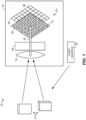
- Fig. 1 is a simplified conceptual diagram of an example 3D (three-dimensional) camera employing a modulator and a polarizing grid array.
- the techniques disclosed herein are to place a grid of optical elements in front of or on the front surface or within the stack of pixel elements of the detecting surface of an imaging sensor array, for example a focal plane array (FPA).
- FPA focal plane array
- These elements can be used to distinguish the signal from different modulation states (including modulated/unmodulated states) and are designed based on the underlying modulation technique.
- such elements could use patterns of polarization elements for phase modulation that results in a polarization change or patterns of transmissive elements for Fabry-Perot cavities and other phase modulation.
- Such elements can be designed and combined in one or more ways to distinguish states of the system, including variations in polarization transmission, spectral transmission, phase transmission, intensity transmission, or similar property of light.
- a compact 3D camera system may be achieved by integrating the elements of a modulated sensor approach described U.S. Patent 8,471,895 B2 issued on June 25, 2013 , (referred to herein as the "'895 patent") with a polarizing or transmission grid array.
- Examples of 3D imaging systems and methods that may be modified to implement the methods and systems described herein are disclosed in the '895 patent at, for example, Figs. 1 -12 and their accompanying written description in the '895 specification.
- Those portions of the '895 patent describe 3D imaging systems that can be configured to perform the methods and to include the polarizing or transmission grid arrays disclosed in the present application.
- the present techniques place the required time-dependent elements in front of each pixel or the array of pixels or photosensitive elements.
- the present techniques uses optical, electro-optic, or other means of affecting the light field in front of each pixel or groups of pixels to affect the photon signal. These optical means may be placed in close proximity to the sensor array, between the sensor array and corresponding optical elements, or in front of such optical elements to allow extraction of time or depth (e.g., z-axis distance) information from the incident light field including time-of-flight information.
- modulator external to the sensor array
- modulators 524, 700-701 1124, 1224 disclosed in the '895 patent to encode the range information eliminates the need for costly custom sensor array or chip development, especially the challenge of scaling chips that can provide high precision timing information which have been limited to about 200 pixels.
- Combining the modulator approach with a polarizing grid coupled and aligned to a sensor array eliminates the need to have two separate sensor arrays and bulky polarizing components such as a polarizing beamsplitter. With a single sensor array, there is alignment and registration between two virtual arrays. The location of each polarization pixel is automatically known relatively to the pixels of the orthogonal polarization in position and angle of any surface normal. This reduces manufacturing and calibration complexity.
- the use of the polarizing grid also greatly reduces the thickness of the glass or other material that is used for polarization separation elements, which reduces the amount of spherical and other optical aberrations.
- these aberrations either degraded the optical performance of the optical system of the 3D camera, or the optical system must be adapted with custom designs to remove or compensate such aberrations.
- the amount of aberration compensation required of optical elements is reduced or eliminated.
- the use of the polarizing grid opens the possibility of making the modulator/polarization separation/sensor array into a closely coupled or monolithic optical assembly that can be used directly with catalog optical lens or imaging elements. In some circumstances, such as wafer scale manufacturing, no lenses or relay optics would need be placed between the optical modulator and the sensor array/polarizing grid. This can reduce the size and cost of the 3D camera system.
- the data streams produced and processed by the 3D camera become simpler since there is only one sensor array and no need to time with other sensor arrays. It also becomes simpler to combine multiple 3D cameras or modules together as described in the'895 patent (for example, to use different range windows and modulation waveforms to extend the range window without worsening the range resolution achievable), such as described in the '895 patent with reference to Fig. 10.
- an electro-optic module 21 includes a grid of polarization elements 18 is placed in front of, or possibly on, the surface of an imaging sensor 20 such as a charge coupled device (CCD) or complementary metal oxide semiconductor (CMOS) array of pixels.
- the polarization grid layer 18 can be placed directly on the surface of the sensor array 20 using an additional step or steps in the lithographic processing.
- the grid layer 18 can be placed on a transparent substrate that is then placed on or in front of the sensor array.
- the polarizing grid 18 can be placed within the layers that are above the detector or electronic sites of a sensor array.
- the polarizing grid 18 is aligned such that the center of each polarizing element 19 is positioned approximately coincident with the center of each pixel 22.
- the grid 18 is arranged so that alternating polarizing elements pass orthogonal polarizations. For example, if the first polarizing element is oriented to pass vertical polarization, the next element in the row or column is oriented to pass horizontal polarization.
- orthogonal circular polarizing element both left-handed and right-handed, can also be used.
- Other configurations may use other patterns of polarizing elements, including elements that pass non-orthogonal polarizations.
- the polarizing elements 18 can be made using a variety of techniques, including metal wire-grid polarizers, thin film polarizing layers, stressed polymers, and elements made of liquid crystal devices as well as any other technique that preferentially passes a particular polarization state over others.
- the polarizing elements can be made of material that can be changed with some control signal, either between each pulse or during the pulse.
- Such elements can be deposited by a variety of methods using film deposition techniques. Some can be created by lithographic techniques such as interspersed exposure (including by multiple beams or wavelengths), etch, and deposition steps. Other such elements can be created by stretching or otherwise stressing materials such as polymers. Some elements can be created by e-beam or laser writing of shapes and structures of the appropriate spacing or dimensions.
- elements that are insensitive to wavelength can be used to support 3D imagery with multiple illumination wavelengths or with broadband illumination.
- elements with narrow acceptance bandwidths can be used as the polarizing elements to more effectively discriminate between desired and undesired wavelengths of light.
- any polarizer grid to sensor array misalignment and non-uniform spacing, non-ideal polarizer performance, and cross-talk between the pixels can be reduced. Because both the polarizer grid and the sensor array can be fabricated using lithographic processes, uniformity of spacing are determined by the mask design, which is normally accurate to nanometer levels. Alignment fiducials can be used to align the two grids and lithographic precision permits accurately matching the pitch of the grid elements.
- Non-ideal polarizer performance would result in location shifts of the minima and maxima of output light. This non-ideal behavior can be handled by calibration of the response at various times. Equally, imperfect polarization contrast (the ratio between the transmission of the transmitted polarization and the rejected polarization) can be managed by proper system calibration. For example, polarization contrasts of approximately 5:1, 10:1, or higher can be used with acceptable performance.
- An effect may be performance changes as the angle content of the incident light changes, for example by changing the F# of the collecting optics.
- Higher f/# optics may be used to reduce cross-talk.
- Some configurations may reduce cross-talk by constructing the polarizing grids to use opaque separator bands or structures between pixels. Such bands or structures reduce the amount of light that can cross from one pixel position to neighboring pixel positions or pixels. In some configurations, such bands or structures may also reduce overall effective transmission efficiency. Other structures can be implemented to reduce cross-talk including structures on either side of the substrate. For example, opaque or reflective structures can be created in the space between pixels that would block light that is transmitted through the grid element from being transmitted to the detector of a neighboring pixel. Such structures or bands may be placed in front of the polarizer array, behind the polarizer array, within the layers of the sensor array, or around the photosite or photosites of the sensor array, as well as within the polarizer array itself.
- guard pixels between the polarization states could be used where the signal is ignored.
- a polarizer element might be nine microns wide with a three micron separator that covers the guard pixels.
- guard pixels could be used with no special separation existing on the grid structure between elements.
- some of the elements of the polarizer array may have no polarization properties or reduced polarization properties, forming the basis to determine the normalization signal.
- Any suitable arrangement of polarization elements and non-polarization elements in the grid can be used depending on the application and system design. These non-polarization elements can be approximately uniform in transmission for multiple wavelengths or they can vary similar to Bayer patterns for color cameras or different filters for IR or thermal cameras or other arrangements at other wavelengths or wavelength regions. For example, they may be opaque or less transmissive of light.
- the polarizer grid elements can be larger than a single pixel of the sensor array, for example 2 x 2, 3 x 3, 4 x 4, or other multiple.
- the elements can also be rectangular, for example, 2 x 1, 3 x 2, or other multiple or aspect ratio or any other arrangement that is non-rectangular in shape. If the grid elements are larger than one pixel, the transmissive elements may be further divided into individual areas that transmit different amounts based on wavelength or angle or other similar optical property.
- the detected signal from the pixels in the sensor array 20 can be binned or otherwise processed to improve the robustness of the measurement, reduce sensitivity to noise or other deleterious effects, or otherwise improve the signal to noise ratio of the individual measurements. Values from different elements or different types of elements can be combined in many ways, depending on the algorithm implemented and the result desired.
- arrays of elements that vary in transmission between elements in some pattern similar to that described above can be employed instead of polarization elements.
- Some elements can be relatively low transmission that may provide the needed finesse for a Fabry-Perot cavity while some elements can be relatively high transmission.
- the high transmission elements (coupled with high transmission elements on the other side of the Fabry Perot cavity) can be used to determine the unmodulated reference signal, including interpolating the signal to the lower transmission elements for determination of the relative modulation signal as described in the base patent.
- the arrangement of these pixels can be grouped in various ways, as described in more detail below.
- the gain of individual pixels, columns, rows, or other arrangements of groups of pixels in the sensor arrays can be adjusted or set to different values to reduce contrast between the groups of elements where there is significant signal or to increase the contrast between pixels or groups of pixels where there is lower signal, thereby increasing the dynamic range of the sensor or 3D camera.
- Some configurations could make use of additional filters that change transmission in front of pixels or groups of pixels. For example, a Bayer pattern RGB filter could be used or other pattern of differing transmissive properties. Such filter elements could also be used where multiple wavelengths of light are used, either for illuminating the scene for the 3D camera or for acquiring specific background or ambient illumination.
- An improved way of eliminating the bulky optics that have been previously used in some 3D cameras to separate polarization states is to place a polarizing element in front of each pixel of a sensor array.
- Such micro-grid polarizing arrays can be used to measure the absolute or relative time-of-flight.
- Absolute distance measurements can be used in a 3D camera, for among other things, to reduce error buildup, particularly where multiple objects or surfaces are within the scene and where they are not connected, or the connection is not visible from the camera.
- Fig. 1 is a simplified perspective-view conceptual diagram of an example 3D camera 10 employing a modulator 14 and a polarizing grid array 14 that receive incoming light 16 through a receiving lens 12.
- the laser illumination (incoming light) 16 is imaged by the lens 12 onto the camera sensor array 20 through the polarizer array 18 with a pattern of polarization directions or transmission parameters such as shown in Fig. 1 .
- the figure shows alternating horizontal and vertical linear polarizers in array 18 arranged to be in front of each pixel 22, but other arrangements and/or circular or elliptical polarization can be used.
- the camera 10 captures 3D information and may also capture image or video from a scene 15 having objects 17 that scatter or reflect illumination light emitted from a light source 25.
- the light source 25 may be integrated with the camera 10 as an illumination subsystem as described in the '895 patent, or alternatively, it may be separated from the camera 10.
- the light source 25 may be any suitable means for illuminating the scene 15, including those described in the '895 patent.
- the electro-optic module 21 may include the optical modulator 14, grid 18, and sensor array 20, as well as an optional polarizer (not shown) located in the optical path before the modulator 14 integrally formed together as a single unit.
- This highly integrated configuration of the electro-optic module 21 may be constructed using the lithographic, etching and deposition techniques described herein.
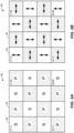
- FIG. 2A-B An example polarizer array 30 arrangement is shown in greater detail in Figs. 2A-B , where S indicates a vertical linear polarizer 32 and P indicates a horizontal linear polarizer 34. (Other arrangements can also be used where S and P can be any two different polarizations, or represent a non-polarizer.)
- the array 30 can be used as array 18 in Fig. 1 .
- the array 30 can be manufactured separately on a glass substrate and then aligned and placed using standard alignment techniques so that each micro-polarizer is positioned such that its center approximately is coincident with the center of the underlying pixel, as shown in Fig. 1 .
- the grid of polarizers 30 can be created directly on the sensor array surface, such as the passivation layer, using standard lithographic techniques.
- a metal layer such as aluminum can be deposited on the surface followed by a photoresist layer, exposing the photoresist with the appropriate mask, etching the exposed photoresist and metal in order to remove preferentially some of the metal layer, and then removing the remaining photoresist and leaving the desired metal structure.
- These metal layers can be ⁇ 1 ⁇ m thick in some cases, or ⁇ 5 ⁇ m thick or other thicknesses as appropriate.
- Other materials or techniques can be used to create the polarizing effect, including etching structures directly into the sensor surface or into the layers deposited above the sensor surface, such as the passivation layer.
- Examples of such materials or techniques is to deposit or arrange stressed polymers or other thin film polarization layers in the gridded pattern. Or liquid crystal devices or structures can be deposited, some with electrically induced patterning. In others, direct etch techniques such as e-beam or laser writing can be used to create a patterned structure. Such layers may be created in a single step or in multiple steps or in multiple layers or in combination of materials and techniques. These techniques and others known to practitioners of similar techniques can be used to create the patterned polarizing elements.
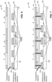
- the polarization element array 30 may also be placed in any of several layers in the stack of layers on the top of the sensor array such as shown in the examples of Figs 5-7 .
- the deposition methods described for creating the polarization elements on the sensor itself (or accompanying layers) can also be used to create polarization elements on a separate transparent or semi-transparent substrate (layers 64 of Fig. 5 , layers 84 of Fig. 6 , and layers 104 of Fig. 7 ) to be place in front of the sensor array.
- a separate transparent or semi-transparent substrate layers 64 of Fig. 5 , layers 84 of Fig. 6 , and layers 104 of Fig. 7
- Such a separate substrate or integrated layer may also have anti-reflection coatings applied to maximize transmission or to minimize stray light.
- Any suitable technique that provides for discrimination between polarization states can be used for the methods and systems disclosed herein; some techniques provide a contrast (or ratio) between desired polarization states and undesired polarization states of > 500:1, some > 100:1, some > 50:1, and some > 10:1.
- the pixel in the (1,1) position provides a response based in large part on the component of the photon flux incident on pixel (1,1) that is polarized vertically.
- the pixel in the (1,2) position provides a response level substantially proportional to the component of the photon flux incident on pixel (1,2) of the alternate polarization. And so on for each pixel across the entire sensor.
- the major polarization axes can be tilted at any angle.
- the major axes of the alternating polarizers are orthogonal.
- the major axes may not be orthogonal.
- a vertical polarizer could be combined with a second polarizer type, the polarization axis forming a 45° angle with respect to the first polarizer.
- Other configurations may use more than two polarizer types, using three, four, or more polarizer types.
- a combination of three polarizer types may have polarization elements forming angles with respect to vertical of 0°, 45°, and 90°, or 0°, 30°, and 60°, or other combination of orientations. In other configurations, these angles may be referenced with respect to the horizontal or any other direction.
- the pattern in which these are arrangements can also vary from the checkerboard pattern shown in Figs. 2A-B .
- the S elements can be arranged on either entire rows or columns, respectively, and the P elements can be arranged on either alternating rows or columns. In some configurations, more of one polarizer type may be present than another or than others.
- the polarizing elements can be sized to be the size of more than one pixel grouped together (an example is shown in Fig. 6 ).
- the polarizing elements can be 11 ⁇ m x 11 ⁇ m if the pixel size or pixel pitch is 5.5 ⁇ m (2 x 2 pixel grouping).
- Such pixel groupings may comprise other suitable numbers of pixels such as 3 x 3, 1 ⁇ 2, 3 ⁇ 4, or any other number or arrangement.
- Any other suitable pixel size or pitch can be used with the arrays described herein, for example 3 ⁇ m or 7 ⁇ m or 15 ⁇ m.
- the pixel size or pitch may be non-regular or all pixels may be of the same size.
- the polarization elements can be aligned to the pixel boundaries, or the centroid of each polarization element aligned to the centroid of the corresponding pixel. In other configurations, at least some of the elements may be misaligned in some patterns that can be assessed using Fourier transform techniques and signal processing or other processing algorithms.
- circular polarizing structures 50 of Fig. 4 can be used to distinguish polarization states as described above.
- the S elements 32 in Figs. 2A-B can instead be right circular polarizing elements 52 and the P elements 34 can be left circular polarizing elements 54 as shown in Fig. 4 .
- Any type of polarizing structure or combination of structures can be used in the disclosed camera system, including pairs of elements with an orthogonal polarization orientation. In some configurations, the polarizing elements may be elliptical polarizing.
- a polarizing grid array 50 is illustrated in Fig. 3 , where some of the pixels 42 are not polarizing structures at all and instead transmit all polarizations.
- the unlabeled elements 42 do not have a polarizing element and the other elements S and P, 44, 46 are as above.
- the non-polarizing elements 42 may all have the same or similar transmission properties, for example transmitting nearly 100% of the light.
- the non-polarizing elements may transmit less than 90% of the incident light or less than 50% or less than 10% of the incident light or any other transmission percentage.
- the transmission percentage may also be patterned for use in high dynamic range (HDR) imaging or other intensity dependent imaging technique such that not all of the transmissive elements have the same transmission percentage.
- polarizing elements may have different transmission values for the corresponding polarization state or elements with different transmission properties may be combined with polarization elements.
- the non-polarizing elements may also be arranged as color filters, or with transmission percentages dependent on color or wavelength, similar to a Bayer pattern.
- the polarizing elements may also be all of the same type (either all S or all P) or any other mixture of polarization types.
- Grids of color filters may be used to create color cameras. For these cameras, the color information is gathered using an array of micro-color filters placed directly in front of the sensor array in a pattern. The most common pattern is known as the Bayer pattern and the filter array is known as a Bayer filter, as described in U.S. patent 3,971,065 to Bayer , which may be used with the element arrays disclosed herein.
- a fraction of the pixels detect the incident light at each wavelength band (red, green, and blue) as a monochromatic signal.
- the color image is then generated using a process known as de-mosaicing, using the measured values and calibrated response curves to calculate the R, G, and B response at the other pixels and then mixing the color values to produce the R, G, and B values that are recorded in the color digital image format, such as JPG.
- These color filter grids may be used to record the color information of the incoming light.
- the normalization image used to normalize the ratio calculated to obtain the depth information is calculated using the response of the pixel to determine the intensity of its associated polarization state combined with the response of the surrounding pixels used to determine the intensity of the opposite polarization state. This is accomplished by interpolating the value for each pixel of the intensity of the orthogonal polarization state using some combination of values of the surrounding pixels.
- the determination of the depth coordinate (z-coordinate) based on this information is simplified since it only uses values within a single array and that have a known relationship and position within the array.
- the relative intensity of the two polarization states for each pixel illustrated in Figs. 2A-B is determined by using the measured value of the polarizing element polarization state and the interpolated value of the other state.
- the normalized combined return for each pixel may be calculated or interpolated based on neighboring pixels in a similar fashion to that used in Bayer-filter based color digital cameras. For example, in an array of elements 30 as illustrated in Figs. 2A-B , where S has a vertical polarizer in front of the pixel and P has a horizontal polarizing element in front of the pixel.
- This interleaved pixel from a single sensor array can reduce optical distortions that may be caused by mis-registration when using bulk polarization separation optics such as a polarizing beamsplitter prism combined with two separate sensor arrays, as shown in Fig. 5 of the '895 patent.
- the 3D range information (z-axis information) for each pixel position is extracted as described in the '895 patent.
- optical and software filters can be applied to change the amount of aliasing present.
- the polarizing element array may be used as an anti-aliasing filter or it can be integrated with other anti-aliasing filters such as holographic elements or other structures.
- the disclosed camera system 10 may also perform in the event of non-ideal polarization states or if there is any dependence of optical performance (either polarization or transmission) on angles of incidence of the returned light.
- the measured performance can be correlated with or corrected to the approximately ideal performance. Offsets and nonlinear response of either the imaging sensor array or the polarizing or transmission elements can be corrected using parameters determined using a calibration step.
- the position of the polarizing grid (including grids with non-polarizing elements) can be aligned to the pixel positions to within some fraction of a pixel.
- the fraction can be ⁇ 0.1 pixels, ⁇ 0.2 pixels, ⁇ 0.5 pixels or other fraction.
- the non-ideal characteristics that can affect the performance for the disclosed single sensor 3D camera can be: polarizer grid to sensor array misalignment and non-uniform spacing, non-ideal (e.g., low contrast) polarizer performance, and cross-talk between the pixels. Because both the polarizer grid and the sensor array may be fabricated using lithographic processes, uniformity of spacing can be determined by the mask design, which is can be accurate to nanometer levels.
- Alignment fiducials can be used to align the two grids and lithographic precision permits accurately matching the pitch of the grid elements.
- Non-ideal polarizer performance would result in shifts of the minima and maxima of the relative response signals over the modulation waveform. This non-ideal behavior can be handled by calibration or characterization of the response at various times and under different conditions.
- materials may be chosen to minimize or prevent relative movement of polarizer elements with respect to pixels over different temperatures, humidity, vibration, or other environmental factors.
- the polarization contrast can be greater than 100:1, for some > 50:1, for some > 20: 1, for some > 10:1, or other contrast ratio that is appropriate for the application.
- An effect can be pixel cross-talk where light passing through a polarization element reaches a neighboring pixel.
- An opaque separator band or guard band between pixels can be used to reduce possible cross-talk.
- such separator bands can be placed as opaque or semi-opaque regions 72 between the polarizing elements 70 as illustrated in side view cross-section of an integrated polarizing array and sensor system 60 in Fig. 5 .
- the array structure 60 includes a polarizing element array layer 62, one or more transparent layers 64, and a sensor substrate layer 66 that includes a substrate 74, sensor pixels 69 and electronic or metallization layer 68.
- the separator bands 72 are shown in Fig. 5 .
- Such opaque regions can be part of the lithographic mask design or can be doped regions or optical absorbing regions similar to the fabrication process for color filters such as Bayer filters.
- Such separator bands can be made of reflective layers or other techniques to reduce the transmission, including transmission based on wavelength or angle of incidence.
- the separator band opaque region 72 can be, for example, any suitable material such a metal, like aluminum, or photo resist, or polymer, or another material such as a semiconductor material like polycrystalline silicon or other types of semiconductor material.
- angles of incidence > 6° (equivalent to ⁇ f/5) may reach the adjacent pixel for some FPA micro-lens designs.
- Some configurations could make use of thicker separation bands, such as 2 ⁇ m or wider, to further reduce cross-talk, depending on the design.
- the separator guard bands 92 are made approximately as wide as the pixel pitch or wider, such that they block a substantial fraction of a pixel 89.
- the array structure 80 includes a polarizing element array layer 82, one or more transparent layers 84, and a sensor substrate layer 86 that includes a substrate 94, sensor pixels 89 and electronic or metallization layer 88.
- Fig. 6 illustrates a design which uses polarizing elements 90 that are 2 pixels wide (for example, 2 x 1 or 2 x 2 or 2 x 3 or other 2D arrangement), with a guard band (G) 92 covering the third pixel 89.
- the guard band 92 can be opaque, reflective, semi-transparent, or transparent or some combination, depending on the design, to reduce cross-talk.
- the guard bands 92 could also be allowed to vary across the polarizing element grid to reduce fabrication costs or for other design purposes.
- Such guard bands 92 can be combined with the variety of arrangements of polarizing elements described above.
- microlens array can be placed in front of or behind the pixelated polarizer or transmission grid structure as appropriate.
- opaque or reflective structures can be included as separator bands or guard bands 112 in the stack of transparent layers 104 in front of the pixel detector layer 106 to reduce the amount of cross-talk light that can reach other pixels.
- An example of this configuration is shown in the integrated array 100 of Fig. 7 .
- the array structure 100 includes a polarizing element array layer 102, one or more transparent layers 104, and a sensor substrate layer 106 that includes a substrate 114, sensor pixels 109 and electronic or metallization layer 108.
- Fig. 7 shows an exemplary placement of opaque structures as vertical walls 112 between pixels 109 to prevent light incident on one polarizing element 110 from reaching a neighbor pixel.
- Such structures 112 can reach the polarizing element grid structure layer 102, or the structures may only reach > 90% of the height between sensor layer 106 and structure 102, or > 75%, or > 50%, or other amount as appropriate for the design of interest.
- these structures 112 can be shaped to be narrower on the top (farthest from the sensor) and wider on the bottom. Other configurations can affect cross-talk by making the structures 112 wider at the top or completely vertical.
- the sensor 109 design itself and metallization layers 108 can also be shaped in similar fashion or made taller to reduce the amount of light that can reach adjacent sensor pixels 109. Other configurations can make use of absorbing material to reduce scattered light or other structures to direct light away from the other pixels.
- the structures 112 can be semi-opaque or semi reflective.
- the distinction between two or more states can be made via other transmission variations rather than polarization variations such as those described above.
- a variable Fabry-Perot etalon can be used to vary the transmission by some means of control similar to that in the '895 patent for polarization states.
- the phase within a Fabry-Perot cavity can be varied by applying a voltage to an electro-optic material, by applying a voltage to a piezo-electric material, by applying a voltage to a liquid crystal, or some other similar means.
- the pixels of an imaging sensor can also be divided into different groups similar to the illustration in Fig. 3 . One group of pixels, such as those indicated by S in Fig.
- Fabry-Perot etalon can have a reflective coating of suitable reflectivity R to achieve the desired finesse of the Fabry-Perot etalon.
- Another group of pixels such as those indicated by P in Fig. 2A , can have reflective or anti-reflective coating that has a different transmission level, such as 100%, or > 99%, or > 95%, or > 90% or > 80% or other desired transmission.
- These high transmission pixels provide a signal value that can be used as the denominator calculated using Eq. (1), where the value for the S pixels can be determined by interpolation similar to the method described above.
- Such groupings of pixels can be arrayed as illustrated in Figs. 2 - 7 or other arrangement that may be desirable. More complex groupings of transmission, with more than two groups, can also be used.
- the reflective coatings may be deposited directly onto the imaging sensor, for example on top of the passivation layer of the sensor array chip. Alternatively, such coatings can be deposited on an additional substrate that can be placed in front of the imaging sensor array with the reflective areas aligned to the pixels of the imaging sensor. Other configurations may have such coatings deposited within the stack of layers that make up the sensor.
- Deposition of these coatings can be performed by techniques known for creating reflective coatings and may use transparent materials such as oxides or fluorides or other similar materials or the coatings may be made of thin or semi-transparent layers of metals or other more opaque or semi-transparent materials, such as gold, silver, aluminum, semiconductor, or other such material. Materials can be chosen to be advantageous at specific wavelengths of interest or may be chosen for use with multiple wavelengths or broadband illumination.
- This transmission patterning can be done on a single substrate or it may be part of a broader stack of coating for electric field application or other transmission patterning.
- the transmission grid can be patterned on elements forming both sides of the Fabry-Perot cavity. Such placement can be selected based on the system design requirements.
- the coating pattern or grouping may be applied in a way to maintain a uniform thickness, either in a single process step or multiple deposition and etch steps.
- FIG. 8 schematically illustrates another example of a 3D imaging sensor system or camera 120.
- Sensor system 120 optionally may include visible imaging subsystem 530 show and described in connection with Fig. 5 of the '895 patent.
- the subsystem 530 is omitted from FIG. 8 for clarity.
- the system 120 includes receiving (Rx) lens 121, band-pass filter (BPF) 122, modulator 124, compensator (Cp.) 125, imaging lens 126, and FPA 129, each of which may be the same as described with respect to the corresponding components illustrated in FIG. 5 of the '895 patent.
- system 120 also includes element array 128, which may be any of the polarizing arrays or transmission-based arrays described herein, for example, with reference to Figs. 2-7 .
- the system 120 can include beamsplitter 123 which is at any suitable position before the modulator (here, between bandpass filter 122 and modulator 124), which directs a portion of the received light to FPA 119, which obtains an image of the scene based thereon. The remainder of the light is transmitted to modulator 124, which modulates the light transmitted there through, and FPA 129 obtains an image of the scene based thereon.
- the images obtained by FPA 119 and FPA 129 may differ in that the former is based on unmodulated light, while the latter is based on modulated light.
- the image obtained by FPA 119 may be used to normalize the image obtained by FPA 129. Specifically, the intensity at any pixel ( i,j ) of FPA 119 may be used as the value I total,i,j in the distance calculations discussed in the '895 patent with reference to equations (8) to (15). Alternatively, in some configurations the intensities measured by FPA 119 are not needed, instead using the demosaiced intensity sum from FPA 129 as described above.
- FPA 119 is used for images a different wavelength or wavelengths, such as visible light or infrared light or other spectral region.
- some of the components shown may be omitted or changed in order.
- the beamsplitter 123 may be replaced by another variety of polarizing plate or optic or for some instances, omitted altogether if the incident polarization state is of sufficient quality.
- the compensator 125 and/or imaging lens can be omitted.
- the bandpass filter 122 can also be omitted for suitable environments where background light can be neglected.
- the components 124 through 128 or some subset thereof can be repeated in other configurations between beamsplitter 123 and the FPA 119.
- the modulation patterns between FPA 119 and 129 can be the same or of different lengths or other differences in shape or structure, as described in the '895 patent.
- the signals obtained from either or both of the FPAs 119, 129 can be combined in algorithms described in the '895 patent.
- FIG. 9 is a flowchart 200 illustrating an example method of capturing a 3D image using the systems described herein.
- a light pulse for example, a laser pulse as described in the '895 patent, emitted from the light source 25. Portions of the light pulse are scattered or reflected from objects in the scene and return to the receiving optics of the 3D camera
- the returned portion of the light pulse is modulated as a function of time by a modulator within the camera.
- the modulator may be any suitable optical modulator, for example a Pockels cell or alternatively, a Fabry-Perot modulator, both described in the '895 patent.
- the modulated returned light pulse portion passes through an element array, such as any of those disclosed herein.
- the element array is arranged to correspond to pixels in a sensor array in a predefined manner.
- the light portion is received at the pixelated sensor array, which generates electrical signals in response to the received light.
- the signals are then processes by a processor, such as a digital signal processor (DSP) or microprocessor, running software to determine time-of-flight information, which can then be used to determine z-axis information to produce a 3D image of the scene.
- DSP digital signal processor
- the systems and methods disclosed herein are able to measure or assess the relative phase or other modulation by using an appropriate grid/array that has groups of distinct elements that pass different signals.
- the type of element in the grid/array is determined based on the needs of the modulation technique chosen. For example, polarizing elements can be used for modulation techniques that change the polarization phase or state of the incoming light. Or transmission elements can be used in a Fabry-Perot arrangement where the phase is modulated. This arrangement allows for at least two different time dependent transmission functions that can be separated by pixels in the sensor array.
Landscapes
- Physics & Mathematics (AREA)
- Engineering & Computer Science (AREA)
- General Physics & Mathematics (AREA)
- Multimedia (AREA)
- Signal Processing (AREA)
- Remote Sensing (AREA)
- Radar, Positioning & Navigation (AREA)
- Computer Networks & Wireless Communication (AREA)
- Optics & Photonics (AREA)
- Electromagnetism (AREA)
- Nonlinear Science (AREA)
- Spectroscopy & Molecular Physics (AREA)
- Polarising Elements (AREA)
- Length Measuring Devices By Optical Means (AREA)
- Measurement Of Optical Distance (AREA)
- Studio Devices (AREA)
- Stereoscopic And Panoramic Photography (AREA)
- Optical Modulation, Optical Deflection, Nonlinear Optics, Optical Demodulation, Optical Logic Elements (AREA)
- Optical Radar Systems And Details Thereof (AREA)
Applications Claiming Priority (2)
| Application Number | Priority Date | Filing Date | Title |
|---|---|---|---|
| US201662301587P | 2016-02-29 | 2016-02-29 | |
| PCT/US2017/020011 WO2017151660A1 (en) | 2016-02-29 | 2017-02-28 | 3d imaging system and method |
Publications (3)
| Publication Number | Publication Date |
|---|---|
| EP3423858A1 EP3423858A1 (en) | 2019-01-09 |
| EP3423858A4 EP3423858A4 (en) | 2019-06-12 |
| EP3423858B1 true EP3423858B1 (en) | 2023-12-06 |
Family
ID=59680144
Family Applications (1)
| Application Number | Title | Priority Date | Filing Date |
|---|---|---|---|
| EP17760645.6A Active EP3423858B1 (en) | 2016-02-29 | 2017-02-28 | 3d imaging system and method |
Country Status (6)
| Country | Link |
|---|---|
| US (1) | US11209664B2 (zh) |
| EP (1) | EP3423858B1 (zh) |
| JP (1) | JP2019513976A (zh) |
| KR (1) | KR20190003480A (zh) |
| CN (1) | CN108780142B (zh) |
| WO (1) | WO2017151660A1 (zh) |
Families Citing this family (31)
| Publication number | Priority date | Publication date | Assignee | Title |
|---|---|---|---|---|
| KR20170009882A (ko) * | 2014-04-26 | 2017-01-25 | 테트라뷰 인코포레이티드 | 3d 이미징의 심도감지용의 강력하고 확대된 광조사 파형을 위한 방법 및 시스템 |
| WO2017210781A1 (en) * | 2016-06-07 | 2017-12-14 | Airy3D Inc. | Light field imaging device and method for depth acquisition and three-dimensional imaging |
| US11056518B2 (en) * | 2016-08-18 | 2021-07-06 | Sony Corporation | Imaging apparatus and imaging method |
| US10448012B2 (en) * | 2016-11-22 | 2019-10-15 | Pixvana, Inc. | System and method for data reduction based on scene content |
| US10505656B2 (en) * | 2017-04-08 | 2019-12-10 | Nokia Solutions And Networks Oy | Optical wavelength selective switches with guard bands |
| WO2019094627A1 (en) * | 2017-11-08 | 2019-05-16 | Arizona Board Of Regents On Behalf Of The University Of Arizona | Imaging method and apparatus using circularly polarized light |
| DE102018205984A1 (de) * | 2018-04-19 | 2019-10-24 | Robert Bosch Gmbh | Vorrichtung und Verfahren zum Bestimmen einer Position von mindestens einem Objekt |
| KR102514487B1 (ko) | 2018-06-07 | 2023-03-27 | 엘지이노텍 주식회사 | 카메라 모듈 및 그의 깊이 정보 추출 방법 |
| US20200041807A1 (en) * | 2018-08-02 | 2020-02-06 | Christie Digital Systems Usa, Inc. | Light emitting diode display with a monolithic wire-grid polarizer for producing three-dimensional images |
| KR102534247B1 (ko) | 2018-10-01 | 2023-05-18 | 삼성전자주식회사 | 편광판을 포함한 3d 이미지 센서, 및 그 3d 이미지 센서를 기반으로 한 깊이 보정방법과 3d 영상 생성방법 |
| JP6978394B2 (ja) * | 2018-11-01 | 2021-12-08 | 京セラ株式会社 | 電磁波検出装置及び情報取得システム |
| JP2020071168A (ja) * | 2018-11-01 | 2020-05-07 | 京セラ株式会社 | 電磁波検出装置および情報取得システム |
| KR102155329B1 (ko) * | 2018-11-09 | 2020-09-11 | 경북대학교 산학협력단 | 라이트 필드 이미징 시스템 |
| TWI696842B (zh) * | 2018-11-16 | 2020-06-21 | 精準基因生物科技股份有限公司 | 飛時測距感測器以及飛時測距方法 |
| EP3884295A4 (en) | 2018-11-21 | 2022-08-17 | The Board of Trustees of the Leland Stanford Junior University | METHODS OF EXTENDED FIELD NANOSECOND IMAGING USING EXTENDED FIELD OPTICAL MODULATORS |
| JP7325949B2 (ja) * | 2018-11-22 | 2023-08-15 | ソニーセミコンダクタソリューションズ株式会社 | 撮像装置及び電子機器 |
| CN111398935B (zh) * | 2018-12-27 | 2022-08-16 | 深圳市速腾聚创科技有限公司 | 激光雷达接收系统 |
| EP3894887A4 (en) | 2019-01-18 | 2022-08-17 | Sense Photonics, Inc. | DIGITAL PIXELS AND THEIR OPERATING METHODS |
| WO2020160349A1 (en) | 2019-01-31 | 2020-08-06 | Sense Photonics, Inc. | Strobe window dependent illumination for flash lidar |
| US11644549B2 (en) * | 2019-03-06 | 2023-05-09 | The University Court Of The University Of Edinburgh | Extended dynamic range and reduced power imaging for LIDAR detector arrays |
| WO2020181048A1 (en) * | 2019-03-06 | 2020-09-10 | Sense Photonics, Inc. | Extended dynamic range and reduced power imaging for lidar detector arrays |
| WO2020259928A1 (en) | 2019-06-27 | 2020-12-30 | Ams International Ag | Imaging system and detection method |
| EP3990942A1 (en) * | 2019-06-27 | 2022-05-04 | ams International AG | Imaging system and detection method |
| WO2021016839A1 (zh) * | 2019-07-30 | 2021-02-04 | 深圳市汇顶科技股份有限公司 | 图像传感器及其制造方法、芯片及手持装置 |
| US11828851B2 (en) | 2020-01-20 | 2023-11-28 | The Board Of Trustees Of The Leland Stanford Junior University | Wide-field resonant electro-optic imaging devices and applications |
| DE102020107450A1 (de) | 2020-03-18 | 2021-09-23 | Audi Aktiengesellschaft | Lidar-Sensoreinrichtung für ein Kraftfahrzeug, Verfahren zum Betrieb einer Lidar-Sensoreinrichtung und Kraftfahrzeug |
| US11723763B2 (en) * | 2020-05-22 | 2023-08-15 | Innovega Inc. | Article of manufacture including occlusion ring having inner/outer regions with orthogonal polarizations |
| CN113884019B (zh) * | 2020-07-03 | 2024-04-05 | 睿镞科技(北京)有限责任公司 | 三维成像系统及方法 |
| WO2022165650A1 (zh) * | 2021-02-02 | 2022-08-11 | 华为技术有限公司 | 一种探测装置、控制方法、融合探测系统及终端 |
| CN113115017B (zh) * | 2021-03-05 | 2022-03-18 | 上海炬佑智能科技有限公司 | 3d成像模组参数检验方法以及3d成像装置 |
| WO2024095471A1 (ja) * | 2022-11-04 | 2024-05-10 | ソニーセミコンダクタソリューションズ株式会社 | 光検出装置及び測距装置 |
Family Cites Families (56)
| Publication number | Priority date | Publication date | Assignee | Title |
|---|---|---|---|---|
| DE1272583B (de) | 1965-04-09 | 1968-07-11 | Philips Patentverwaltung | Verfahren zur photooptischen Aufzeichnung bzw. Speicherung von aus Einzelsymbolen bestehenden Informationen |
| US3644017A (en) | 1968-12-02 | 1972-02-22 | Baird Atomic Inc | Electro-optic light modulator with area selection |
| JPS5636405B2 (zh) | 1971-09-18 | 1981-08-24 | ||
| CH667340A5 (de) | 1985-04-30 | 1988-09-30 | Cerberus Ag | Lichtschranke. |
| US4967270A (en) | 1989-05-08 | 1990-10-30 | Kaman Aerospace Corporation | Lidar system incorporating multiple cameras for obtaining a plurality of subimages |
| US4935616A (en) | 1989-08-14 | 1990-06-19 | The United States Of America As Represented By The Department Of Energy | Range imaging laser radar |
| US6736321B2 (en) | 1995-12-18 | 2004-05-18 | Metrologic Instruments, Inc. | Planar laser illumination and imaging (PLIIM) system employing wavefront control methods for reducing the power of speckle-pattern noise digital images acquired by said system |
| US5200793A (en) | 1990-10-24 | 1993-04-06 | Kaman Aerospace Corporation | Range finding array camera |
| US5162861A (en) | 1991-04-01 | 1992-11-10 | Tamburino Louis A | Laser imaging and ranging system using one camera |
| US5157451A (en) | 1991-04-01 | 1992-10-20 | John Taboada | Laser imaging and ranging system using two cameras |
| US5144482A (en) | 1991-05-13 | 1992-09-01 | Gould Dennis R | Three dimensional viewing apparatus including a stack of transparent plates and related method |
| US5686990A (en) | 1992-12-08 | 1997-11-11 | The Charles Stark Draper Laboratory, Inc. | Optical source isolator with polarization maintaining optical fiber and aspheric collimating and focusing lens |
| US5394413A (en) | 1994-02-08 | 1995-02-28 | Massachusetts Institute Of Technology | Passively Q-switched picosecond microlaser |
| DE4439298A1 (de) | 1994-11-07 | 1996-06-13 | Rudolf Prof Dr Ing Schwarte | 3D-Kamera nach Laufzeitverfahren |
| US6088086A (en) | 1995-09-11 | 2000-07-11 | Sandia Corporation | Range determination for scannerless imaging |
| US5892575A (en) * | 1996-05-10 | 1999-04-06 | Massachusetts Institute Of Technology | Method and apparatus for imaging a scene using a light detector operating in non-linear geiger-mode |
| US7796081B2 (en) | 1997-10-22 | 2010-09-14 | Intelligent Technologies International, Inc. | Combined imaging and distance monitoring for vehicular applications |
| US7046711B2 (en) | 1999-06-11 | 2006-05-16 | High Q Laser Production Gmbh | High power and high gain saturation diode pumped laser means and diode array pumping device |
| EP1214609B1 (en) | 1999-09-08 | 2004-12-15 | 3DV Systems Ltd. | 3d imaging system |
| US6515737B2 (en) | 2000-01-04 | 2003-02-04 | The Regents Of The University Of California | High-resolution imaging and target designation through clouds or smoke |
| US6456793B1 (en) | 2000-08-03 | 2002-09-24 | Eastman Kodak Company | Method and apparatus for a color scannerless range imaging system |
| US7140543B2 (en) | 2000-11-24 | 2006-11-28 | Metrologic Instruments, Inc. | Planar light illumination and imaging device with modulated coherent illumination that reduces speckle noise induced by coherent illumination |
| US7444013B2 (en) | 2001-08-10 | 2008-10-28 | Stmicroelectronics, Inc. | Method and apparatus for recovering depth using multi-plane stereo and spatial propagation |
| US20040041082A1 (en) | 2001-11-27 | 2004-03-04 | Harmon Gary R. | Molecular sensing array |
| US6707054B2 (en) * | 2002-03-21 | 2004-03-16 | Eastman Kodak Company | Scannerless range imaging system having high dynamic range |
| US6781763B1 (en) | 2002-04-01 | 2004-08-24 | The United States Of America As Represented By The Secretary Of The Air Force | Image analysis through polarization modulation and combination |
| US7224382B2 (en) | 2002-04-12 | 2007-05-29 | Image Masters, Inc. | Immersive imaging system |
| US7257278B2 (en) | 2003-02-26 | 2007-08-14 | Hewlett-Packard Development Company, L.P. | Image sensor for capturing and filtering image data |
| US7301138B2 (en) | 2003-12-19 | 2007-11-27 | General Atomics | Method and apparatus for dual polarization imaging |
| US7236235B2 (en) * | 2004-07-06 | 2007-06-26 | Dimsdale Engineering, Llc | System and method for determining range in 3D imaging systems |
| JP4566685B2 (ja) | 2004-10-13 | 2010-10-20 | 株式会社トプコン | 光画像計測装置及び光画像計測方法 |
| US7535617B2 (en) | 2005-08-18 | 2009-05-19 | The United States Of America As Represented By The Secretary Of The Army | Portable acousto-optical spectrometers |
| US9182228B2 (en) | 2006-02-13 | 2015-11-10 | Sony Corporation | Multi-lens array system and method |
| US7995191B1 (en) | 2006-06-29 | 2011-08-09 | Sandia Corporation | Scannerless laser range imaging using loss modulation |
| US7667762B2 (en) | 2006-08-01 | 2010-02-23 | Lifesize Communications, Inc. | Dual sensor video camera |
| US7751109B1 (en) | 2006-09-14 | 2010-07-06 | The United States Of America As Represented By The Secretary Of The Army | Electro-optic shutter |
| JP4403162B2 (ja) | 2006-09-29 | 2010-01-20 | 株式会社東芝 | 立体画像表示装置および立体画像の作製方法 |
| US8259203B2 (en) | 2007-12-05 | 2012-09-04 | Electro Scientific Industries, Inc. | Method and apparatus for achieving panchromatic response from a color-mosaic imager |
| JP4450076B2 (ja) * | 2008-01-17 | 2010-04-14 | パナソニック株式会社 | 三次元画像再生装置 |
| EP2265993B8 (en) * | 2008-03-28 | 2021-07-07 | Contrast, Inc. | Whole beam image splitting system |
| US8471895B2 (en) | 2008-11-25 | 2013-06-25 | Paul S. Banks | Systems and methods of high resolution three-dimensional imaging |
| US8823848B2 (en) * | 2009-06-11 | 2014-09-02 | The Arizona Board Of Regents On Behalf Of The University Of Arizona | Microgrid imaging polarimeters with frequency domain reconstruction |
| US8228417B1 (en) * | 2009-07-15 | 2012-07-24 | Adobe Systems Incorporated | Focused plenoptic camera employing different apertures or filtering at different microlenses |
| US8736670B2 (en) * | 2009-12-07 | 2014-05-27 | Photon-X, Inc. | 3D visualization system |
| US20110175981A1 (en) | 2010-01-19 | 2011-07-21 | Chun-Hung Lai | 3d color image sensor |
| CN201707438U (zh) * | 2010-05-28 | 2011-01-12 | 中国科学院合肥物质科学研究院 | 基于led阵列共透镜tof深度测量的三维成像系统 |
| US8444275B2 (en) | 2010-08-12 | 2013-05-21 | Eastman Kodak Company | Light source control for projector with multiple pulse-width modulated light sources |
| KR101680762B1 (ko) * | 2010-10-29 | 2016-11-29 | 삼성전자주식회사 | 3d 카메라용 빔스플리터 및 상기 빔스플리터를 채용한 3차원 영상 획득 장치 |
| US9479743B2 (en) | 2011-06-01 | 2016-10-25 | Gvbb Holdings S.A.R.L. | Single lens 3-D camera |
| JP5982751B2 (ja) * | 2011-08-04 | 2016-08-31 | ソニー株式会社 | 画像処理装置、および画像処理方法、並びにプログラム |
| WO2013052781A1 (en) | 2011-10-07 | 2013-04-11 | Massachusetts Institute Of Technology | Method and apparatus to determine depth information for a scene of interest |
| US9177983B2 (en) * | 2012-01-23 | 2015-11-03 | Omnivision Technologies, Inc. | Image sensor with optical filters having alternating polarization for 3D imaging |
| WO2013114891A1 (ja) * | 2012-02-03 | 2013-08-08 | パナソニック株式会社 | 撮像装置および撮像システム |
| WO2014125529A1 (ja) * | 2013-02-15 | 2014-08-21 | パナソニック株式会社 | 画像処理装置および内視鏡 |
| CA2937497A1 (en) * | 2014-01-22 | 2015-10-08 | Polaris Sensor Technologies, Inc. | Polarization imaging for facial recognition enhancement system and method |
| KR20170009882A (ko) * | 2014-04-26 | 2017-01-25 | 테트라뷰 인코포레이티드 | 3d 이미징의 심도감지용의 강력하고 확대된 광조사 파형을 위한 방법 및 시스템 |
-
2017
- 2017-02-28 WO PCT/US2017/020011 patent/WO2017151660A1/en active Application Filing
- 2017-02-28 EP EP17760645.6A patent/EP3423858B1/en active Active
- 2017-02-28 US US15/445,560 patent/US11209664B2/en active Active
- 2017-02-28 CN CN201780017336.0A patent/CN108780142B/zh active Active
- 2017-02-28 KR KR1020187028140A patent/KR20190003480A/ko not_active Application Discontinuation
- 2017-02-28 JP JP2018545214A patent/JP2019513976A/ja active Pending
Also Published As
| Publication number | Publication date |
|---|---|
| EP3423858A1 (en) | 2019-01-09 |
| CN108780142A (zh) | 2018-11-09 |
| KR20190003480A (ko) | 2019-01-09 |
| CN108780142B (zh) | 2023-10-31 |
| WO2017151660A1 (en) | 2017-09-08 |
| US11209664B2 (en) | 2021-12-28 |
| EP3423858A4 (en) | 2019-06-12 |
| US20170248796A1 (en) | 2017-08-31 |
| JP2019513976A (ja) | 2019-05-30 |
Similar Documents
| Publication | Publication Date | Title |
|---|---|---|
| EP3423858B1 (en) | 3d imaging system and method | |
| Maruyama et al. | 3.2-MP Back-Illuminated Polarization Image Sensor With Four-Directional Air-Gap Wire Grid and 2.5-$\mu $ m Pixels | |
| KR102391632B1 (ko) | 광 필드 이미징 장치 및 깊이 획득 및 3차원 이미징 방법 | |
| EP2816389B1 (en) | A method for producing a mirror for a Fabry-Perot interferomete | |
| US10317205B2 (en) | Depth measurement using a phase grating | |
| US10438365B2 (en) | Imaging device, subject information acquisition method, and computer program | |
| US11902494B2 (en) | System and method for glint reduction | |
| CN108417644B (zh) | 一种红外探测器的封装结构以及封装方法 | |
| US7330266B2 (en) | Stationary fourier transform spectrometer | |
| JP2007322128A (ja) | カメラモジュール | |
| US20220050205A1 (en) | Electro-optic modulator and methods of using and manufacturing same for three-dimensional imaging | |
| US20220221733A1 (en) | Light Field Imaging Device and Method for 3D Sensing | |
| EP3700197B1 (en) | Imaging device and method, and image processing device and method | |
| US20180166488A1 (en) | Image sensor and electronic device | |
| JP2014003433A (ja) | 撮像装置 | |
| CN107917759A (zh) | 基于阶梯相位反射镜的偏振干涉成像光谱仪及制作方法 | |
| CN114365019A (zh) | 深度信息图像采集装置和电子设备 | |
| Brückner et al. | Advanced artificial compound-eye imaging systems | |
| US20240063240A1 (en) | Light state imaging pixel | |
| Drysdale | Plasmonic angle sensitive pixel for digital imagers | |
| TW202413899A (zh) | 多光譜光學感測器、攝影機系統及視差補償方法 | |
| CN117949087A (zh) | 一种基于偏振调制阵列和消色差四面角锥棱镜的偏振相机 | |
| Möller | Full frame 3D snapshot: Possibilities and limitations of 3D image acquisition without scanning |
Legal Events
| Date | Code | Title | Description |
|---|---|---|---|
| STAA | Information on the status of an ep patent application or granted ep patent |
Free format text: STATUS: THE INTERNATIONAL PUBLICATION HAS BEEN MADE |
|
| PUAI | Public reference made under article 153(3) epc to a published international application that has entered the european phase |
Free format text: ORIGINAL CODE: 0009012 |
|
| STAA | Information on the status of an ep patent application or granted ep patent |
Free format text: STATUS: REQUEST FOR EXAMINATION WAS MADE |
|
| 17P | Request for examination filed |
Effective date: 20180926 |
|
| AK | Designated contracting states |
Kind code of ref document: A1 Designated state(s): AL AT BE BG CH CY CZ DE DK EE ES FI FR GB GR HR HU IE IS IT LI LT LU LV MC MK MT NL NO PL PT RO RS SE SI SK SM TR |
|
| AX | Request for extension of the european patent |
Extension state: BA ME |
|
| RIC1 | Information provided on ipc code assigned before grant |
Ipc: G01S 17/89 20060101AFI20190201BHEP Ipc: G01S 7/481 20060101ALI20190201BHEP Ipc: H04N 13/271 20180101ALI20190201BHEP Ipc: G01S 7/499 20060101ALI20190201BHEP Ipc: H04N 13/218 20180101ALI20190201BHEP Ipc: H04N 13/296 20180101ALI20190201BHEP Ipc: H04N 13/254 20180101ALI20190201BHEP |
|
| STAA | Information on the status of an ep patent application or granted ep patent |
Free format text: STATUS: REQUEST FOR EXAMINATION WAS MADE |
|
| REG | Reference to a national code |
Ref country code: DE Ref legal event code: R079 Ref document number: 602017077228 Country of ref document: DE Free format text: PREVIOUS MAIN CLASS: G01S0007481000 Ipc: G01S0017890000 Ref country code: DE Ref legal event code: R079 Free format text: PREVIOUS MAIN CLASS: G01S0007481000 Ipc: G01S0017890000 |
|
| DAV | Request for validation of the european patent (deleted) | ||
| DAX | Request for extension of the european patent (deleted) | ||
| A4 | Supplementary search report drawn up and despatched |
Effective date: 20190514 |
|
| RIC1 | Information provided on ipc code assigned before grant |
Ipc: G01S 17/89 20060101AFI20190508BHEP Ipc: G01S 7/481 20060101ALI20190508BHEP Ipc: G01S 7/499 20060101ALI20190508BHEP Ipc: H04N 13/296 20180101ALI20190508BHEP Ipc: H04N 13/271 20180101ALI20190508BHEP Ipc: H04N 13/254 20180101ALI20190508BHEP Ipc: H04N 13/218 20180101ALI20190508BHEP |
|
| STAA | Information on the status of an ep patent application or granted ep patent |
Free format text: STATUS: THE APPLICATION IS DEEMED TO BE WITHDRAWN |
|
| 18D | Application deemed to be withdrawn |
Effective date: 20191214 |
|
| 19U | Interruption of proceedings before grant |
Effective date: 20200226 |
|
| STAA | Information on the status of an ep patent application or granted ep patent |
Free format text: STATUS: REQUEST FOR EXAMINATION WAS MADE |
|
| 19W | Proceedings resumed before grant after interruption of proceedings |
Effective date: 20210301 |
|
| D18D | Application deemed to be withdrawn (deleted) | ||
| RAP3 | Party data changed (applicant data changed or rights of an application transferred) |
Owner name: NLIGHT, INC. |
|
| STAA | Information on the status of an ep patent application or granted ep patent |
Free format text: STATUS: EXAMINATION IS IN PROGRESS |
|
| 17Q | First examination report despatched |
Effective date: 20220224 |
|
| GRAP | Despatch of communication of intention to grant a patent |
Free format text: ORIGINAL CODE: EPIDOSNIGR1 |
|
| STAA | Information on the status of an ep patent application or granted ep patent |
Free format text: STATUS: GRANT OF PATENT IS INTENDED |
|
| INTG | Intention to grant announced |
Effective date: 20230508 |
|
| P01 | Opt-out of the competence of the unified patent court (upc) registered |
Effective date: 20230523 |
|
| GRAJ | Information related to disapproval of communication of intention to grant by the applicant or resumption of examination proceedings by the epo deleted |
Free format text: ORIGINAL CODE: EPIDOSDIGR1 |
|
| STAA | Information on the status of an ep patent application or granted ep patent |
Free format text: STATUS: EXAMINATION IS IN PROGRESS |
|
| GRAP | Despatch of communication of intention to grant a patent |
Free format text: ORIGINAL CODE: EPIDOSNIGR1 |
|
| STAA | Information on the status of an ep patent application or granted ep patent |
Free format text: STATUS: GRANT OF PATENT IS INTENDED |
|
| INTC | Intention to grant announced (deleted) | ||
| GRAS | Grant fee paid |
Free format text: ORIGINAL CODE: EPIDOSNIGR3 |
|
| GRAA | (expected) grant |
Free format text: ORIGINAL CODE: 0009210 |
|
| STAA | Information on the status of an ep patent application or granted ep patent |
Free format text: STATUS: THE PATENT HAS BEEN GRANTED |
|
| INTG | Intention to grant announced |
Effective date: 20231011 |
|
| AK | Designated contracting states |
Kind code of ref document: B1 Designated state(s): AL AT BE BG CH CY CZ DE DK EE ES FI FR GB GR HR HU IE IS IT LI LT LU LV MC MK MT NL NO PL PT RO RS SE SI SK SM TR |
|
| REG | Reference to a national code |
Ref country code: CH Ref legal event code: EP |
|
| REG | Reference to a national code |
Ref country code: DE Ref legal event code: R096 Ref document number: 602017077228 Country of ref document: DE |
|
| REG | Reference to a national code |
Ref country code: IE Ref legal event code: FG4D |
|
| REG | Reference to a national code |
Ref country code: LT Ref legal event code: MG9D |
|
| PG25 | Lapsed in a contracting state [announced via postgrant information from national office to epo] |
Ref country code: GR Free format text: LAPSE BECAUSE OF FAILURE TO SUBMIT A TRANSLATION OF THE DESCRIPTION OR TO PAY THE FEE WITHIN THE PRESCRIBED TIME-LIMIT Effective date: 20240307 |
|
| REG | Reference to a national code |
Ref country code: NL Ref legal event code: MP Effective date: 20231206 |
|
| PG25 | Lapsed in a contracting state [announced via postgrant information from national office to epo] |
Ref country code: LT Free format text: LAPSE BECAUSE OF FAILURE TO SUBMIT A TRANSLATION OF THE DESCRIPTION OR TO PAY THE FEE WITHIN THE PRESCRIBED TIME-LIMIT Effective date: 20231206 |
|
| PG25 | Lapsed in a contracting state [announced via postgrant information from national office to epo] |
Ref country code: ES Free format text: LAPSE BECAUSE OF FAILURE TO SUBMIT A TRANSLATION OF THE DESCRIPTION OR TO PAY THE FEE WITHIN THE PRESCRIBED TIME-LIMIT Effective date: 20231206 |
|
| PG25 | Lapsed in a contracting state [announced via postgrant information from national office to epo] |
Ref country code: LT Free format text: LAPSE BECAUSE OF FAILURE TO SUBMIT A TRANSLATION OF THE DESCRIPTION OR TO PAY THE FEE WITHIN THE PRESCRIBED TIME-LIMIT Effective date: 20231206 Ref country code: GR Free format text: LAPSE BECAUSE OF FAILURE TO SUBMIT A TRANSLATION OF THE DESCRIPTION OR TO PAY THE FEE WITHIN THE PRESCRIBED TIME-LIMIT Effective date: 20240307 Ref country code: ES Free format text: LAPSE BECAUSE OF FAILURE TO SUBMIT A TRANSLATION OF THE DESCRIPTION OR TO PAY THE FEE WITHIN THE PRESCRIBED TIME-LIMIT Effective date: 20231206 Ref country code: BG Free format text: LAPSE BECAUSE OF FAILURE TO SUBMIT A TRANSLATION OF THE DESCRIPTION OR TO PAY THE FEE WITHIN THE PRESCRIBED TIME-LIMIT Effective date: 20240306 |
|
| PGFP | Annual fee paid to national office [announced via postgrant information from national office to epo] |
Ref country code: GB Payment date: 20240219 Year of fee payment: 8 |
|
| REG | Reference to a national code |
Ref country code: AT Ref legal event code: MK05 Ref document number: 1638919 Country of ref document: AT Kind code of ref document: T Effective date: 20231206 |
|
| PG25 | Lapsed in a contracting state [announced via postgrant information from national office to epo] |
Ref country code: NL Free format text: LAPSE BECAUSE OF FAILURE TO SUBMIT A TRANSLATION OF THE DESCRIPTION OR TO PAY THE FEE WITHIN THE PRESCRIBED TIME-LIMIT Effective date: 20231206 |