EP3422823A1 - Flexible printed circuit board - Google Patents
Flexible printed circuit board Download PDFInfo
- Publication number
- EP3422823A1 EP3422823A1 EP17756732.8A EP17756732A EP3422823A1 EP 3422823 A1 EP3422823 A1 EP 3422823A1 EP 17756732 A EP17756732 A EP 17756732A EP 3422823 A1 EP3422823 A1 EP 3422823A1
- Authority
- EP
- European Patent Office
- Prior art keywords
- dielectric layer
- ground
- signal line
- disposed
- circuit board
- Prior art date
- Legal status (The legal status is an assumption and is not a legal conclusion. Google has not performed a legal analysis and makes no representation as to the accuracy of the status listed.)
- Pending
Links
Images


Classifications
-
- H—ELECTRICITY
- H05—ELECTRIC TECHNIQUES NOT OTHERWISE PROVIDED FOR
- H05K—PRINTED CIRCUITS; CASINGS OR CONSTRUCTIONAL DETAILS OF ELECTRIC APPARATUS; MANUFACTURE OF ASSEMBLAGES OF ELECTRICAL COMPONENTS
- H05K1/00—Printed circuits
- H05K1/02—Details
- H05K1/11—Printed elements for providing electric connections to or between printed circuits
- H05K1/118—Printed elements for providing electric connections to or between printed circuits specially for flexible printed circuits, e.g. using folded portions
-
- H—ELECTRICITY
- H05—ELECTRIC TECHNIQUES NOT OTHERWISE PROVIDED FOR
- H05K—PRINTED CIRCUITS; CASINGS OR CONSTRUCTIONAL DETAILS OF ELECTRIC APPARATUS; MANUFACTURE OF ASSEMBLAGES OF ELECTRICAL COMPONENTS
- H05K1/00—Printed circuits
- H05K1/02—Details
- H05K1/0213—Electrical arrangements not otherwise provided for
- H05K1/0216—Reduction of cross-talk, noise or electromagnetic interference
- H05K1/0218—Reduction of cross-talk, noise or electromagnetic interference by printed shielding conductors, ground planes or power plane
- H05K1/0219—Printed shielding conductors for shielding around or between signal conductors, e.g. coplanar or coaxial printed shielding conductors
- H05K1/0221—Coaxially shielded signal lines comprising a continuous shielding layer partially or wholly surrounding the signal lines
-
- H—ELECTRICITY
- H05—ELECTRIC TECHNIQUES NOT OTHERWISE PROVIDED FOR
- H05K—PRINTED CIRCUITS; CASINGS OR CONSTRUCTIONAL DETAILS OF ELECTRIC APPARATUS; MANUFACTURE OF ASSEMBLAGES OF ELECTRICAL COMPONENTS
- H05K1/00—Printed circuits
- H05K1/18—Printed circuits structurally associated with non-printed electric components
- H05K1/189—Printed circuits structurally associated with non-printed electric components characterised by the use of a flexible or folded printed circuit
-
- H—ELECTRICITY
- H05—ELECTRIC TECHNIQUES NOT OTHERWISE PROVIDED FOR
- H05K—PRINTED CIRCUITS; CASINGS OR CONSTRUCTIONAL DETAILS OF ELECTRIC APPARATUS; MANUFACTURE OF ASSEMBLAGES OF ELECTRICAL COMPONENTS
- H05K3/00—Apparatus or processes for manufacturing printed circuits
- H05K3/46—Manufacturing multilayer circuits
-
- H—ELECTRICITY
- H05—ELECTRIC TECHNIQUES NOT OTHERWISE PROVIDED FOR
- H05K—PRINTED CIRCUITS; CASINGS OR CONSTRUCTIONAL DETAILS OF ELECTRIC APPARATUS; MANUFACTURE OF ASSEMBLAGES OF ELECTRICAL COMPONENTS
- H05K1/00—Printed circuits
- H05K1/02—Details
- H05K1/0213—Electrical arrangements not otherwise provided for
- H05K1/0216—Reduction of cross-talk, noise or electromagnetic interference
- H05K1/0218—Reduction of cross-talk, noise or electromagnetic interference by printed shielding conductors, ground planes or power plane
- H05K1/0224—Patterned shielding planes, ground planes or power planes
- H05K1/0225—Single or multiple openings in a shielding, ground or power plane
-
- H—ELECTRICITY
- H05—ELECTRIC TECHNIQUES NOT OTHERWISE PROVIDED FOR
- H05K—PRINTED CIRCUITS; CASINGS OR CONSTRUCTIONAL DETAILS OF ELECTRIC APPARATUS; MANUFACTURE OF ASSEMBLAGES OF ELECTRICAL COMPONENTS
- H05K1/00—Printed circuits
- H05K1/02—Details
- H05K1/0213—Electrical arrangements not otherwise provided for
- H05K1/0237—High frequency adaptations
- H05K1/024—Dielectric details, e.g. changing the dielectric material around a transmission line
-
- H—ELECTRICITY
- H05—ELECTRIC TECHNIQUES NOT OTHERWISE PROVIDED FOR
- H05K—PRINTED CIRCUITS; CASINGS OR CONSTRUCTIONAL DETAILS OF ELECTRIC APPARATUS; MANUFACTURE OF ASSEMBLAGES OF ELECTRICAL COMPONENTS
- H05K2201/00—Indexing scheme relating to printed circuits covered by H05K1/00
- H05K2201/05—Flexible printed circuits [FPCs]
-
- H—ELECTRICITY
- H05—ELECTRIC TECHNIQUES NOT OTHERWISE PROVIDED FOR
- H05K—PRINTED CIRCUITS; CASINGS OR CONSTRUCTIONAL DETAILS OF ELECTRIC APPARATUS; MANUFACTURE OF ASSEMBLAGES OF ELECTRICAL COMPONENTS
- H05K2201/00—Indexing scheme relating to printed circuits covered by H05K1/00
- H05K2201/09—Shape and layout
- H05K2201/09209—Shape and layout details of conductors
- H05K2201/09218—Conductive traces
- H05K2201/09236—Parallel layout
-
- H—ELECTRICITY
- H05—ELECTRIC TECHNIQUES NOT OTHERWISE PROVIDED FOR
- H05K—PRINTED CIRCUITS; CASINGS OR CONSTRUCTIONAL DETAILS OF ELECTRIC APPARATUS; MANUFACTURE OF ASSEMBLAGES OF ELECTRICAL COMPONENTS
- H05K2201/00—Indexing scheme relating to printed circuits covered by H05K1/00
- H05K2201/09—Shape and layout
- H05K2201/09209—Shape and layout details of conductors
- H05K2201/095—Conductive through-holes or vias
- H05K2201/09618—Via fence, i.e. one-dimensional array of vias
-
- H—ELECTRICITY
- H05—ELECTRIC TECHNIQUES NOT OTHERWISE PROVIDED FOR
- H05K—PRINTED CIRCUITS; CASINGS OR CONSTRUCTIONAL DETAILS OF ELECTRIC APPARATUS; MANUFACTURE OF ASSEMBLAGES OF ELECTRICAL COMPONENTS
- H05K2201/00—Indexing scheme relating to printed circuits covered by H05K1/00
- H05K2201/10—Details of components or other objects attached to or integrated in a printed circuit board
- H05K2201/10007—Types of components
- H05K2201/10098—Components for radio transmission, e.g. radio frequency identification [RFID] tag, printed or non-printed antennas
-
- H—ELECTRICITY
- H05—ELECTRIC TECHNIQUES NOT OTHERWISE PROVIDED FOR
- H05K—PRINTED CIRCUITS; CASINGS OR CONSTRUCTIONAL DETAILS OF ELECTRIC APPARATUS; MANUFACTURE OF ASSEMBLAGES OF ELECTRICAL COMPONENTS
- H05K3/00—Apparatus or processes for manufacturing printed circuits
- H05K3/46—Manufacturing multilayer circuits
- H05K3/4611—Manufacturing multilayer circuits by laminating two or more circuit boards
- H05K3/4626—Manufacturing multilayer circuits by laminating two or more circuit boards characterised by the insulating layers or materials
- H05K3/4635—Manufacturing multilayer circuits by laminating two or more circuit boards characterised by the insulating layers or materials laminating flexible circuit boards using additional insulating adhesive materials between the boards
-
- H—ELECTRICITY
- H05—ELECTRIC TECHNIQUES NOT OTHERWISE PROVIDED FOR
- H05K—PRINTED CIRCUITS; CASINGS OR CONSTRUCTIONAL DETAILS OF ELECTRIC APPARATUS; MANUFACTURE OF ASSEMBLAGES OF ELECTRICAL COMPONENTS
- H05K3/00—Apparatus or processes for manufacturing printed circuits
- H05K3/46—Manufacturing multilayer circuits
- H05K3/4697—Manufacturing multilayer circuits having cavities, e.g. for mounting components
Definitions
- the present disclosure relates to a flexible printed circuit board.
- a radio frequency (RF) signal line is provided in a terminal such as a mobile phone, a tablet PC, a notebook, and the like.
- the RF signal line according to the related art is mounted in the form of a coaxial cable.
- the flexible printed circuit board is used in recent years because the space utilization in the wireless terminal is deteriorated.
- two or more RF signal lines are used for transmitting a short distance communication signal such as WIFI and/or a wireless mobile communication signal such as 3G and 4G.
- An object of the present invention is to provide a flexible printed circuit board in which a signal interference and a signal loss are minimized to be optimized for a wireless terminal such as a notebook while a plurality of signal lines are arranged on a plane in parallel to each other to realize a thin thickness.
- a flexible printed circuit board includes: a first substrate part including a first signal line; and a second substrate part including a second signal line parallel to the first signal line, wherein the first substrate part and the second substrate part are disposed on the same plane with a shielding part therebetween.
- the flexible printed circuit board may further include: a first dielectric layer; a second dielectric layer disposed to be spaced a predetermined distance from the first dielectric layer in a vertical direction; a pair of first side grounds laminated to be spaced a predetermined from each other on a bottom surface of the first dielectric layer; a pair of second side grounds laminated to be spaced a predetermined from each other on a plane of the second dielectric layer; a first central ground disposed between the pair of first side grounds and laminated on the bottom surface of the first dielectric layer; and a second central ground disposed between the pair of second side grounds and laminated on the plane of the second dielectric layer, wherein the first signal line and the second signal line may be disposed with the first central ground and the second central ground therebetween.
- the first signal line may be disposed between each of the second side grounds and the second central ground and formed on the plane of the second dielectric layer, and the second signal line may be disposed between each of the first side grounds and the first central ground and formed on the bottom surface of the first dielectric layer.
- a first ground layer may be laminated on a plane of the first dielectric layer
- a second ground layer may be laminated on a bottom surface of the second dielectric layer, and facing surfaces of the first dielectric layer and the second dielectric layer, the first central ground and the second central ground, and the first side ground and the second side ground may be coupled to each other by using a coupling part as a medium.
- a first ground layer may be laminated on a plane of the first dielectric layer, a second ground layer may be laminated on a bottom surface of the second dielectric layer, and the first central ground and the second central ground, and the first side ground and the second side ground may be coupled to each other by using a coupling part as a medium, wherein an air layer may be formed in a space through which the first dielectric layer and the second dielectric layer face each other so that the first signal line and the second signal line are exposed to the air layer.
- the flexible printed circuit board according to the present invention may further include: a first dielectric layer; a second dielectric layer disposed to be spaced a predetermined distance from the first dielectric layer in a vertical direction; a third dielectric layer spaced a predetermined distance from the second dielectric layer in the vertical direction, wherein the third dielectric layer and the second dielectric layer are disposed with the first dielectric layer therebetween; a pair of first side grounds laminated to be spaced a predetermined from each other on a plane of the first dielectric layer; a pair of second side grounds laminated to be spaced a predetermined from each other on a bottom surface of the first dielectric layer; a first central ground disposed between the pair of first side grounds and laminated on the plane of the first dielectric layer; and a second central ground disposed between the pair of second side grounds and laminated on the bottom surface of the first dielectric layer, wherein the first signal line and the second signal line may be disposed with the first central ground and the second central ground therebetween.
- the first signal line may be disposed between the second side ground and the second central ground and formed on the bottom surface of the first dielectric layer, and the second signal line may be disposed between the first side ground and the first central ground and formed on the plane of the first dielectric layer.
- a first ground layer may be laminated on a plane of the second dielectric layer
- a second ground layer may be laminated on a bottom surface of the third dielectric layer
- facing surfaces of the first dielectric layer and the second dielectric layer, facing surfaces of the first central ground and the second dielectric layer, facing surfaces of the first side ground and the second dielectric layer, and facing surfaces of the second signal line and the second dielectric layer may be coupled to each other by using a first coupling part as a medium
- facing surfaces of the first dielectric layer and the third dielectric layer, facing surfaces of the second central ground and the third dielectric layer, facing surfaces of the second side ground and the third dielectric layer, and facing surfaces of the first signal line and the third dielectric layer may be coupled to each other by using a second coupling part as a medium.
- a first ground layer may be laminated on a plane of the second dielectric layer, a second ground layer may be laminated on a bottom surface of the third dielectric layer, and an air layer may be formed between the first dielectric layer on which the first signal line is formed and the third dielectric layer and between the first dielectric layer on which the second signal line is formed and the second dielectric layer so that the first signal line and the second signal line are exposed to the air layer.
- the first substrate part and the second substrate part may be divided with respect to the first central ground and the second central ground.
- the flexible printed circuit board may further include: a first via hole formed to pass through the first substrate part in the vertical direction; a second via hole formed to pass through the second substrate part in the vertical direction; and third and fourth via holes passing through the shielding part in the vertical direction and formed to be spaced a predetermined distance from each other in a width direction.
- the first via hole to the fourth via hole may be disposed on the same line in the width direction.
- the first via hole and the third via hole may be disposed on the same first line in the width direction
- the second via hole and the fourth via hole may be disposed on the same second line in the width direction
- the first line and the second line may be formed to alternate with each other.
- a plurality of circular ground holes may be formed to be spaced a predetermined distance from each other in a longitudinal direction of the first signal line in the first ground layer disposed on the plane of the first signal line, a plurality of rectangular ground holes may be formed to be spaced a predetermined distance from each other in a longitudinal direction of the second signal line in the first ground layer disposed on the plane of the second signal line, a plurality of rectangular ground holes may be formed to be spaced a predetermined distance from each other in the longitudinal direction of the first signal line in the second ground layer disposed on the bottom surface of the first signal line, and a plurality of circular ground holes may be formed to be spaced a predetermined distance from each other in the longitudinal direction of the second signal line in the second ground layer disposed on the bottom surface of the second signal line.
- a coaxial cable may be connected to one end of each of the first signal line and the second signal line.
- each of the first signal line and the second signal line may extend in a left and right direction to form a "T" shape.
- a first antenna and a second antenna may be coupled to both ends that are formed to extend from the other end in the left and right direction.
- a first antenna and a second antenna may be formed to extend from both the ends in the left and right direction.
- the plurality of signal lines may be arranged on the plane in parallel to each other to realize the thin thickness.
- the signal interference occurring between the first signal line and the second signal line may be minimized.
- the signal loss may be minimized.
- FIG. 1 is a cross-sectional view of a flexible printed circuit board according to a first embodiment of the present invention.
- the flexible printed circuit board includes a first substrate part 10, a second substrate part 20, and a shielding part 30.
- the first substrate part 10 and the second substrate part 20 are disposed on the same plane with the shielding part 30 therebetween.
- a first signal line T1 formed on the first substrate part 10 and a second signal line T2 formed on the second substrate part 20 are disposed in parallel to each other.
- the flexible printed circuit board according to the present invention may be realized with a thin thickness. Since the first signal line T1 and the second signal line T2 are disposed with the shielding part 30 therebetween, a signal loss due to mutual signal interference may be minimized.
- the flexible printed circuit board according to the present invention may include a first dielectric layer E1, a second dielectric layer E2, a pair of first side grounds S1, a pair of second side grounds S2, a first central ground C1, and a second central ground C2.
- the first dielectric layer E1 and the second dielectric layer E2 are disposed in parallel to be spaced a predetermined distance from each other in a vertical direction and have shape corresponding to each other.
- the pair of first side grounds S1 are laminated to be spaced a predetermined distance from each other on a bottom surface of the first dielectric layer E1, and the pair of second side grounds S2 are laminated to be spaced a predetermined distance from each other on a plane of the second dielectric layer E2.
- the bottom surface of the first dielectric layer E1 and the plane of the second dielectric layer E2 may face each other, bottom surfaces of the pair of first side grounds S1 and planes of the pair of second side grounds S2 may also face each other and be spaced a predetermined distance from each other in the vertical direction.
- the first central ground C1 is laminated on the bottom surface of the first dielectric layer E1 and disposed between the pair of first side grounds S1
- the second central ground C2 is laminated on the plane of the second dielectric layer E2 and disposed between the pair of second side grounds S2.
- the first central ground C1 and the second central ground C2 have shapes corresponding to each other and are disposed in parallel to be spaced a predetermined distance from each other in the vertical direction.
- the first substrate part 10 on which the first signal line T1 is formed and the second substrate part 20 on which the second signal line T2 is formed are disposed on the same plane with the shielding part 30 therebetween.
- one region may be defined as the first substrate part 10
- the other region may be defined as the second substrate part 20 with respect to a region in which the first central ground C1 and the second central ground C2 are disposed.
- the shielding part 30 may be defined as the region in which the first central ground C1 and the second central ground C2 are disposed.
- first central ground C1 and the second central ground C2 may extend to the regions of the first substrate part 10 and the second substrate part 20 as well as the region of the shielding part 30.
- the first signal line T1 and the second signal line T2 are disposed with the above-described first central ground C1 and second central ground C2 therebetween to prevent signal interference occurring between the first signal line T1 and the second signal line T2 from occurring.
- first signal line T1 is formed on the plane of the second dielectric layer E2
- second signal line T2 is formed on the bottom surface of the first dielectric layer E1 in FIG. 3
- the arrangement structure of the first signal line T1 and the second signal line T2 may be variously changed depending on designer's intension.
- the bottom surface of the first dielectric layer E1 and the plane of the second dielectric layer E2, facing surfaces of the first central ground C1 and the second central ground C2, facing surfaces of the first side ground S1 and the second side ground S2, facing surfaces of the first signal line T1 and the first dielectric layer E1, and facing surfaces of the second signal line T2 and the second dielectric layer E2 may be coupled to each other by using a coupling part P as a medium.
- the coupling part P may be a dielectric that is deformed during high-temperature press coupling or an adhesion medium such as a bonding sheet.
- the structure of the coupling part P may be variously deformed and applied depending on designer's intension.
- a flexible printed circuit board according to a second embodiment of the present invention is the same as that according to the foregoing first embodiment except for an installation region of a coupling part P.
- the coupling part P is installed so that the first signal line T1 and the second signal line T2 are exposed to an air layer. That is, only the facing areas of the first side ground S1 and the second side ground S2 and the facing areas of the first central ground C1 and the second central ground C2 are coupled to each other by using the coupling part P as a medium.
- the air layer may be formed between the facing surfaces of the first dielectric layer E1 and the second dielectric layer E2, and the first signal line T1 and the second signal line T2 may be exposed to the air layer having a low dielectric constant. Thus, capacitance may be reduced to minimize a signal loss.
- a three-layered dielectric layer structure according to third and fourth embodiments may be applied to the flexible printed circuit board according to the present invention.
- a first substrate part 10 and a second substrate part 20 may also be disposed on the same plane with a shielding part 30 therebetween.
- this specific configuration will be described.
- the flexible printed circuit board may include a first dielectric layer E1, a second dielectric layer E2, a third dielectric layer E3, a pair of first side grounds S1, a pair of second side grounds S2, a first central ground C1, and a second central ground C2.
- the second dielectric layer E2 is disposed to be spaced a predetermined distance from each other upward, and the third dielectric layer E3 is disposed to be spaced a predetermined distance from each other downward with respect to the first dielectric layer E1.
- the first dielectric layer E1, the second dielectric layer E2, and the third dielectric layer E3 are formed in parallel to each other with shapes corresponding to each other.
- the pair of first side grounds S1 are laminated to be spaced a predetermined distance from each other on a plane of the first dielectric layer E1
- the pair of second side grounds S2 are laminated to be spaced a predetermined distance from each other on a bottom surface of the second dielectric layer E2.
- the first side ground S1 and the second side ground S2 may have the same shape and the same area. This will be variously deformed and used depending on designer's intension.
- the first central ground C1 is disposed between the pair of first side grounds S1 and laminated on a plane of the first dielectric layer E1
- the second central ground C2 is disposed between the pair of second side grounds S2 and laminated on a bottom surface of the first dielectric layer E1.
- one region may be defined as a first substrate part 10, and the other region may be defined as a second substrate part 20 with respect to a region in which the first central ground C1 and the second central ground C2 are disposed.
- a shielding part 30 may be defined as the region in which the first central ground C1 and the second central ground C2 are disposed.
- first central ground C1 and the second central ground C2 may extend to the regions of the first substrate part 10 and the second substrate part 20 as well as the region of the shielding part 30.
- the first signal line T1 is disposed between the second side ground S2 disposed at one side of the first dielectric layer E1 and the second central ground C2, and the second signal line T2 is disposed between the first side ground S1 disposed at the other side of the first dielectric layer E1 and the first central ground C1. That is, signal interference occurring between the first signal line T1 and the second signal line T2 may be prevented by the first central ground C1 and the second central ground C2.
- the signal interference occurring due to other components disposed on upper and lower portions of the flexible printed circuit board may be prevented.
- facing surfaces of the first dielectric layer E1 and the second dielectric layer E2, facing surfaces of the first central ground C1 and the second dielectric layer E2, facing surface of the first side ground S1 and the second dielectric layer E2, and facing surface of the second signal line T2 and the second dielectric layer E2 are coupled to each other by using a first coupling part P1 as a medium
- facing surface of the first dielectric layer E1 and the third dielectric layer E3, facing surface of the second central ground C2 and the third dielectric layer E3, facing surface of the second side ground S2 and the third dielectric layer E3, and facing surface of the first signal line T1 and the third dielectric layer E3 may be coupled to each other by using the second coupling part P2 as a medium.
- Each of the first coupling part P1 and the second coupling part P2 may be a dielectric that is deformed during high-temperature press coupling or an adhesion medium such as a bonding sheet.
- the structures of the first coupling part P1 and the second coupling part P2 may be variously deformed and applied depending on designer's intension.
- a flexible printed circuit board according to a fourth embodiment of the present invention is the same as that according to the foregoing third embodiment except for installation regions of a first coupling part P1 and a second coupling part P2.
- a first substrate part 10 is disposed at one side of a shielding part 30, and a second substrate part 20 is disposed at the other side of the shielding part 30 with respect to the shielding part 30.
- a second signal ling T2 is disposed between a first central ground C1 of a region of the shielding part 30 and a first side ground S1 of a region of the second substrate part 20, and a first signal ling T1 is disposed between a second central ground C2 of the region of the first substrate part 10 and a second central ground C2 of the region of the shielding part 30.
- the first coupling part P1 is disposed between a first dielectric layer E1 and a second dielectric layer E2 to couple the first and second dielectric layers E1 and E2 to each other, and the second coupling part P2 is disposed between the first dielectric layer E1 and a third dielectric layer E3 to couple the first and third dielectric layers E1 and E3 to each other.
- the second coupling part P2 is removed from the region in which the first signal line T1 of the first substrate part 10 is installed so that the first signal line T1 is exposed to an air layer
- the first coupling part P1 is removed from the region in which the second signal line T2 of the second substrate part 20 so that the second signal line T2 is exposed to the air layer.
- the first side ground S1 and the second dielectric layer E2 the first dielectric layer E1 and the second electric layer E2, and the first central ground C1 and the second dielectric layer E2 are coupled to each other by using the first coupling part P1 as a medium.
- the first central ground C1 and the second dielectric layer E2 may also be coupled to each other by using the first coupling part P1 as the medium.
- the second signal line T2 is exposed to the air layer.
- the second side ground S2 and the third dielectric layer E3, the first dielectric layer E1 and the third electric layer E3, and the second central ground C2 and the third dielectric layer E3 are coupled to each other by using the second coupling part P2 as a medium.
- the second central ground C2 and the third dielectric layer E3 may also be coupled to each other by using the second coupling part P2 as the medium.
- the first signal line T1 is exposed to the air layer.
- the first signal line T1 and the second signal line T2 are exposed to the air layer having a low dielectric constant. Thus, capacitance may be reduced to minimize the signal loss.
- a plurality of via holes V1, V2, V3, and V4 may be formed in the flexible printed circuit board according to the present invention.
- the first ground layer G1 is laminated on a plane of the first dielectric layer E1
- the second ground layer G2 is laminated on a bottom surface of the second dielectric layer E2.
- the first via hole V1 is formed to pass through the region of the first substrate part 10 in a vertical direction
- the second via hole V2 is formed to pass through the region of the second substrate part 20 disposed at the other side with respect to the shielding part 30 in the vertical direction.
- the third via hole V3 and the fourth via hole V4 are formed to pass through the shielding part 30 and to be spaced a predetermined distance from each other in a width direction are formed in the shielding part 30.
- the first via hole V1 and the second via hole V2 may pass through the first ground layer G1, the first dielectric layer E1, the first side ground S1, the coupling part P, the second side ground S2, and the second ground layer G2 so that the first side ground S1, the second side ground S2, the first ground layer G1, and the second ground layer G2 are electrically conducted.
- the third via hole V3 and the fourth via hole V4 may pass through the first ground layer G1, the first dielectric layer E1, the first central ground C1, the coupling part P, the second central ground C2, the second dielectric layer E2, and the second ground layer G2 so that the first central ground C1, the second central ground C2, the first ground layer G1, and the second ground layer G2 are electrically conducted.
- the first via hole V1, the second via hole V2, the third via hole V3, and the fourth via hole V4 may be formed.
- the first via hole V1 may be formed in the region of the first substrate part 10
- the second via hole may be formed in the region of the second substrate part 20
- the third via hole V3 and the fourth via hole V4 may be formed in the region of the shielding part 30.
- the first via hole V1 and the second via hole V2 may pass through the first ground layer G1, the second dielectric layer E2, the coupling part P1, the first side ground S1, the first dielectric layer E1, the second side ground S2, the second coupling part P2, the third dielectric layer E3, and the second ground layer G2 so that the first side ground S1, the second side ground S2, the first ground layer G1, and the second ground layer G2 are electrically conducted.
- the third via hole V3 and the fourth via hole V4 may pass through the first ground layer G1, the second dielectric layer E2, the first coupling part P1, the first central ground C1, the first dielectric layer E1, the second central ground C2, the second coupling part P2, the third dielectric layer E3, and the second ground layer G2 so that the first central ground C1, the second central ground C2, the first ground layer G1, and the second ground layer G2 are electrically conducted.
- the first via hole V1, the second via hole V2, the third via hole V3, and the fourth via hole V4 may be disposed on the same line in the width direction of the flexible printed circuit board.
- the first via hole V1 and the third via hole V3 are disposed on the same first line L1 in the width direction
- the second via hole V2 and the fourth via hole V4 are disposed on the same second line L2 in the width direction.
- the first line L1 and the second line L2 may be formed to alternate with each other.
- the first central ground C1 and the second central ground C2 may improve a shielding effect.
- a distance between the third via hole V3 and the fourth via hole V4, which are disposed in the shielding part 30, may be reduced to maximize the shielding effect.
- a rectangular ground hole H is formed in the first ground layer G1 or the second ground layer G2, which is disposed close to the first signal line T1 and the second signal line T2 in the vertical direction.
- a rectangular ground hole H is formed in the first ground layer G1 or the second ground layer G2, which is disposed close to the first signal line T1 and the second signal line T2, and a circular ground hole H is formed in the first ground layer G1 or the second ground layer G2, which is relatively remote.
- FIGS. 7(a) to 7(d) are views illustrating the ground hole H of the flexible printed circuit board according to the first to fourth embodiments of the present invention.
- the rectangular ground hole H is formed in the second ground layer G2 that is disposed close to the first signal line T1
- the circular ground hole H is formed in the first ground layer G1 that is disposed away from the first signal line T1.
- the rectangular ground hole H is formed in the first ground layer G1 that is disposed close to the second signal line T2
- the circular ground hole H is formed in the second ground layer E2 that is disposed away from the second signal line T2.
- a flexible printed circuit board 210 is connected to one end of a coaxial cable 110.
- assembly may be easy, the flexible printed circuit board 210 may be minimized in length, signal loss may be reduced, and manufacturing costs may be reduced.
- the flexible printed circuit board 210 is connected to the coaxial cable 110 through one selected from a connector C or soldering.
- the flexible printed circuit board 210 has a "T" shape, and a first antenna 212 and a second antenna 214 are connected to both ends of the flexible printed circuit board 210.
- the first antenna 212 connected to the flexible printed circuit board 210 transmits and receives a short distance communication signal such as WIFI, and the second antenna 214 transmits and receives a wireless mobile communication signal such as 3G and 4G.
- one end of both ends of the flexible printed circuit board 210 which is connected to the first antenna 212, has a length greater than that of the other end connected to the second antenna 214 in order to minimize signal interference of the first antenna 212 and the second antenna 214.
- the flexible printed circuit board 210 may further include a first antenna 212 and a second antenna 214, which extend from both ends of the flexible printed circuit board 210 in a left and right direction. That is, the first antenna 212 and the second antenna 214 are integrated with both the ends of the flexible printed circuit board 210.
- the flexible printed circuit board is formed in a " ⁇ " shape. Also, it is preferable that a position from which the second antenna 214 is formed to extend is disposed far away from a center of the flexible printed circuit board 210 in a vertical direction when compared to the position from which the first antenna 212 is formed to extend.
Abstract
Description
- The present disclosure relates to a flexible printed circuit board.
- A radio frequency (RF) signal line is provided in a terminal such as a mobile phone, a tablet PC, a notebook, and the like. The RF signal line according to the related art is mounted in the form of a coaxial cable. In the case of being mounted in the form of the coaxial cable, it is general that the flexible printed circuit board is used in recent years because the space utilization in the wireless terminal is deteriorated.
- With the development of communication technology, two or more RF signal lines are used for transmitting a short distance communication signal such as WIFI and/or a wireless mobile communication signal such as 3G and 4G.
- As described above, when the coaxial connector is used as each of the RF signal lines to prevent signals from interfering with each other, a space occupied by the thickness of the coaxial connector itself and a fixing body for fixing he coaxial connector increases in the wireless terminal. To solve such the spatial problem, there is a need to use the flexible printed circuit board.
- However, when the flexible printed circuit board is used, since the RF signal lines different from each other have to be spaced apart from each other so as to solve the signal interference problem, there is also a limitation in solving the spatial problem within the wireless terminal.
- It should be understood that the foregoing description of the background art is merely for the purpose of promoting a better understanding of the background of the present invention, and is not to be construed as admission that the prior art is known to those skilled in the art.
- An object of the present invention is to provide a flexible printed circuit board in which a signal interference and a signal loss are minimized to be optimized for a wireless terminal such as a notebook while a plurality of signal lines are arranged on a plane in parallel to each other to realize a thin thickness.
- To achieve this object, a flexible printed circuit board according to the present invention includes: a first substrate part including a first signal line; and a second substrate part including a second signal line parallel to the first signal line, wherein the first substrate part and the second substrate part are disposed on the same plane with a shielding part therebetween.
- The flexible printed circuit board may further include: a first dielectric layer; a second dielectric layer disposed to be spaced a predetermined distance from the first dielectric layer in a vertical direction; a pair of first side grounds laminated to be spaced a predetermined from each other on a bottom surface of the first dielectric layer; a pair of second side grounds laminated to be spaced a predetermined from each other on a plane of the second dielectric layer; a first central ground disposed between the pair of first side grounds and laminated on the bottom surface of the first dielectric layer; and a second central ground disposed between the pair of second side grounds and laminated on the plane of the second dielectric layer, wherein the first signal line and the second signal line may be disposed with the first central ground and the second central ground therebetween.
- The first signal line may be disposed between each of the second side grounds and the second central ground and formed on the plane of the second dielectric layer, and the second signal line may be disposed between each of the first side grounds and the first central ground and formed on the bottom surface of the first dielectric layer.
- A first ground layer may be laminated on a plane of the first dielectric layer, a second ground layer may be laminated on a bottom surface of the second dielectric layer, and facing surfaces of the first dielectric layer and the second dielectric layer, the first central ground and the second central ground, and the first side ground and the second side ground may be coupled to each other by using a coupling part as a medium.
- A first ground layer may be laminated on a plane of the first dielectric layer, a second ground layer may be laminated on a bottom surface of the second dielectric layer, and the first central ground and the second central ground, and the first side ground and the second side ground may be coupled to each other by using a coupling part as a medium, wherein an air layer may be formed in a space through which the first dielectric layer and the second dielectric layer face each other so that the first signal line and the second signal line are exposed to the air layer.
- The flexible printed circuit board according to the present invention may further include: a first dielectric layer; a second dielectric layer disposed to be spaced a predetermined distance from the first dielectric layer in a vertical direction; a third dielectric layer spaced a predetermined distance from the second dielectric layer in the vertical direction, wherein the third dielectric layer and the second dielectric layer are disposed with the first dielectric layer therebetween; a pair of first side grounds laminated to be spaced a predetermined from each other on a plane of the first dielectric layer; a pair of second side grounds laminated to be spaced a predetermined from each other on a bottom surface of the first dielectric layer; a first central ground disposed between the pair of first side grounds and laminated on the plane of the first dielectric layer; and a second central ground disposed between the pair of second side grounds and laminated on the bottom surface of the first dielectric layer, wherein the first signal line and the second signal line may be disposed with the first central ground and the second central ground therebetween.
- The first signal line may be disposed between the second side ground and the second central ground and formed on the bottom surface of the first dielectric layer, and the second signal line may be disposed between the first side ground and the first central ground and formed on the plane of the first dielectric layer.
- A first ground layer may be laminated on a plane of the second dielectric layer, a second ground layer may be laminated on a bottom surface of the third dielectric layer, facing surfaces of the first dielectric layer and the second dielectric layer, facing surfaces of the first central ground and the second dielectric layer, facing surfaces of the first side ground and the second dielectric layer, and facing surfaces of the second signal line and the second dielectric layer may be coupled to each other by using a first coupling part as a medium, and facing surfaces of the first dielectric layer and the third dielectric layer, facing surfaces of the second central ground and the third dielectric layer, facing surfaces of the second side ground and the third dielectric layer, and facing surfaces of the first signal line and the third dielectric layer may be coupled to each other by using a second coupling part as a medium.
- A first ground layer may be laminated on a plane of the second dielectric layer, a second ground layer may be laminated on a bottom surface of the third dielectric layer, and an air layer may be formed between the first dielectric layer on which the first signal line is formed and the third dielectric layer and between the first dielectric layer on which the second signal line is formed and the second dielectric layer so that the first signal line and the second signal line are exposed to the air layer.
- The first substrate part and the second substrate part may be divided with respect to the first central ground and the second central ground.
- The flexible printed circuit board may further include: a first via hole formed to pass through the first substrate part in the vertical direction; a second via hole formed to pass through the second substrate part in the vertical direction; and third and fourth via holes passing through the shielding part in the vertical direction and formed to be spaced a predetermined distance from each other in a width direction.
- The first via hole to the fourth via hole may be disposed on the same line in the width direction.
- The first via hole and the third via hole may be disposed on the same first line in the width direction, the second via hole and the fourth via hole may be disposed on the same second line in the width direction, and the first line and the second line may be formed to alternate with each other.
- A plurality of circular ground holes may be formed to be spaced a predetermined distance from each other in a longitudinal direction of the first signal line in the first ground layer disposed on the plane of the first signal line, a plurality of rectangular ground holes may be formed to be spaced a predetermined distance from each other in a longitudinal direction of the second signal line in the first ground layer disposed on the plane of the second signal line, a plurality of rectangular ground holes may be formed to be spaced a predetermined distance from each other in the longitudinal direction of the first signal line in the second ground layer disposed on the bottom surface of the first signal line, and a plurality of circular ground holes may be formed to be spaced a predetermined distance from each other in the longitudinal direction of the second signal line in the second ground layer disposed on the bottom surface of the second signal line.
- A coaxial cable may be connected to one end of each of the first signal line and the second signal line.
- The other end of each of the first signal line and the second signal line may extend in a left and right direction to form a "T" shape.
- A first antenna and a second antenna may be coupled to both ends that are formed to extend from the other end in the left and right direction.
- A first antenna and a second antenna may be formed to extend from both the ends in the left and right direction.
- According to the present invention, the following various effects can be realized.
- First, the plurality of signal lines may be arranged on the plane in parallel to each other to realize the thin thickness.
- Second, the signal interference occurring between the first signal line and the second signal line may be minimized.
- Third, the signal loss may be minimized.
-
-
FIG. 1 is a cross-sectional view of a flexible printed circuit board according to a first embodiment of the present invention, -
FIG. 2 is a cross-sectional view of a flexible printed circuit board according to a second embodiment of the present invention, -
FIG. 3 is a cross-sectional view of a flexible printed circuit board according to a third embodiment of the present invention, -
FIG. 4 is a cross-sectional view of a flexible printed circuit board according to a fourth embodiment of the present invention, -
FIGS. 5(a) and 5(b) are views illustrating a via hole of a flexible printed circuit board according to different embodiments of the present invention, -
FIGS. 6(a) and 6(b) are views illustrating a ground hole of a flexible printed circuit board according to different embodiments of the present invention, -
FIGS. 7(a) to 7(d) are views illustrating a ground hole of the flexible printed circuit board according to the first to fourth embodiments of the present invention, -
FIG 8(a) is a view illustrating a state in which an antenna is coupled to the flexible printed circuit board according to the present invention, and -
FIG. 8(b) is a view illustrating a state in which the antenna is integrated with the flexible printed circuit board according to the present invention. - The objectives, specific advantages, and novel features of the present invention will become more apparent from the following detailed description and embodiments taken in conjunction with the accompanying drawings. It should be noted that the reference numerals are added to the components of the drawings in the present specification with the same numerals as possible, even if they are illustrated in other drawings. Also, it will be understood that although the terms such as 'first' and 'second' are used herein to describe various elements, these elements should not be limited by these terms. The terms are only used to distinguish one component from other components. Moreover, detailed descriptions related to well-known functions or configurations will be ruled out in order not to unnecessarily obscure subject matters of the present disclosure.
- Hereinafter, specific embodiments will be described in detail with reference to the accompanying drawings.
-
FIG. 1 is a cross-sectional view of a flexible printed circuit board according to a first embodiment of the present invention. - As illustrated in
FIG. 1 , the flexible printed circuit board according to the present invention includes afirst substrate part 10, asecond substrate part 20, and ashielding part 30. - The
first substrate part 10 and thesecond substrate part 20 are disposed on the same plane with theshielding part 30 therebetween. Thus, a first signal line T1 formed on thefirst substrate part 10 and a second signal line T2 formed on thesecond substrate part 20 are disposed in parallel to each other. - As described above, since the
first substrate part 10 and thesecond substrate part 20 are disposed on the same plane, the flexible printed circuit board according to the present invention may be realized with a thin thickness. Since the first signal line T1 and the second signal line T2 are disposed with theshielding part 30 therebetween, a signal loss due to mutual signal interference may be minimized. - The flexible printed circuit board according to the present invention may include a first dielectric layer E1, a second dielectric layer E2, a pair of first side grounds S1, a pair of second side grounds S2, a first central ground C1, and a second central ground C2.
- The first dielectric layer E1 and the second dielectric layer E2 are disposed in parallel to be spaced a predetermined distance from each other in a vertical direction and have shape corresponding to each other.
- The pair of first side grounds S1 are laminated to be spaced a predetermined distance from each other on a bottom surface of the first dielectric layer E1, and the pair of second side grounds S2 are laminated to be spaced a predetermined distance from each other on a plane of the second dielectric layer E2.
- The bottom surface of the first dielectric layer E1 and the plane of the second dielectric layer E2 may face each other, bottom surfaces of the pair of first side grounds S1 and planes of the pair of second side grounds S2 may also face each other and be spaced a predetermined distance from each other in the vertical direction.
- The first central ground C1 is laminated on the bottom surface of the first dielectric layer E1 and disposed between the pair of first side grounds S1, and the second central ground C2 is laminated on the plane of the second dielectric layer E2 and disposed between the pair of second side grounds S2. The first central ground C1 and the second central ground C2 have shapes corresponding to each other and are disposed in parallel to be spaced a predetermined distance from each other in the vertical direction.
- As described above, the
first substrate part 10 on which the first signal line T1 is formed and thesecond substrate part 20 on which the second signal line T2 is formed are disposed on the same plane with the shieldingpart 30 therebetween. Here, one region may be defined as thefirst substrate part 10, and the other region may be defined as thesecond substrate part 20 with respect to a region in which the first central ground C1 and the second central ground C2 are disposed. The shieldingpart 30 may be defined as the region in which the first central ground C1 and the second central ground C2 are disposed. - Here, the first central ground C1 and the second central ground C2 may extend to the regions of the
first substrate part 10 and thesecond substrate part 20 as well as the region of the shieldingpart 30. - The first signal line T1 and the second signal line T2 are disposed with the above-described first central ground C1 and second central ground C2 therebetween to prevent signal interference occurring between the first signal line T1 and the second signal line T2 from occurring.
- Also, although the first signal line T1 is formed on the plane of the second dielectric layer E2, and the second signal line T2 is formed on the bottom surface of the first dielectric layer E1 in
FIG. 3 , the arrangement structure of the first signal line T1 and the second signal line T2 may be variously changed depending on designer's intension. - The bottom surface of the first dielectric layer E1 and the plane of the second dielectric layer E2, facing surfaces of the first central ground C1 and the second central ground C2, facing surfaces of the first side ground S1 and the second side ground S2, facing surfaces of the first signal line T1 and the first dielectric layer E1, and facing surfaces of the second signal line T2 and the second dielectric layer E2 may be coupled to each other by using a coupling part P as a medium.
- The coupling part P may be a dielectric that is deformed during high-temperature press coupling or an adhesion medium such as a bonding sheet. The structure of the coupling part P may be variously deformed and applied depending on designer's intension.
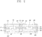
- As illustrated in
FIG 2 , a flexible printed circuit board according to a second embodiment of the present invention is the same as that according to the foregoing first embodiment except for an installation region of a coupling part P. - In description of the flexible printed circuit board according to the second embodiment of the present invention, descriptions with respect to other components except for the coupling part P will be derived from those of the flexible printed circuit board according to the foregoing first embodiment, and thus, the installation region of the coupling part P, which is different from that of the coupling part according to the first embodiment, will be mainly described below.
- The coupling part P is installed so that the first signal line T1 and the second signal line T2 are exposed to an air layer. That is, only the facing areas of the first side ground S1 and the second side ground S2 and the facing areas of the first central ground C1 and the second central ground C2 are coupled to each other by using the coupling part P as a medium.
- The air layer may be formed between the facing surfaces of the first dielectric layer E1 and the second dielectric layer E2, and the first signal line T1 and the second signal line T2 may be exposed to the air layer having a low dielectric constant. Thus, capacitance may be reduced to minimize a signal loss.
- Although the two-layered dielectric layer structure according to the first and second embodiments are applied to the flexible printed circuit board according to the present invention, a three-layered dielectric layer structure according to third and fourth embodiments may be applied to the flexible printed circuit board according to the present invention.
- In the flexible printed circuit board according to the third and fourth embodiments of the present invention, a
first substrate part 10 and asecond substrate part 20 may also be disposed on the same plane with a shieldingpart 30 therebetween. Hereinafter, this specific configuration will be described. - As illustrated in
FIG. 3 , the flexible printed circuit board according to the third embodiment of the present invention may include a first dielectric layer E1, a second dielectric layer E2, a third dielectric layer E3, a pair of first side grounds S1, a pair of second side grounds S2, a first central ground C1, and a second central ground C2. - The second dielectric layer E2 is disposed to be spaced a predetermined distance from each other upward, and the third dielectric layer E3 is disposed to be spaced a predetermined distance from each other downward with respect to the first dielectric layer E1. The first dielectric layer E1, the second dielectric layer E2, and the third dielectric layer E3 are formed in parallel to each other with shapes corresponding to each other.
- Also, the pair of first side grounds S1 are laminated to be spaced a predetermined distance from each other on a plane of the first dielectric layer E1, and the pair of second side grounds S2 are laminated to be spaced a predetermined distance from each other on a bottom surface of the second dielectric layer E2.
- The first side ground S1 and the second side ground S2 may have the same shape and the same area. This will be variously deformed and used depending on designer's intension.
- The first central ground C1 is disposed between the pair of first side grounds S1 and laminated on a plane of the first dielectric layer E1, and the second central ground C2 is disposed between the pair of second side grounds S2 and laminated on a bottom surface of the first dielectric layer E1.
- As described in the first and second embodiments of the present invention, in a third embodiment, one region may be defined as a
first substrate part 10, and the other region may be defined as asecond substrate part 20 with respect to a region in which the first central ground C1 and the second central ground C2 are disposed. A shieldingpart 30 may be defined as the region in which the first central ground C1 and the second central ground C2 are disposed. - Here, the first central ground C1 and the second central ground C2 may extend to the regions of the
first substrate part 10 and thesecond substrate part 20 as well as the region of the shieldingpart 30. - The first signal line T1 is disposed between the second side ground S2 disposed at one side of the first dielectric layer E1 and the second central ground C2, and the second signal line T2 is disposed between the first side ground S1 disposed at the other side of the first dielectric layer E1 and the first central ground C1. That is, signal interference occurring between the first signal line T1 and the second signal line T2 may be prevented by the first central ground C1 and the second central ground C2.
- Also, in the case of the three-layered dielectric layer structure, the signal interference occurring due to other components disposed on upper and lower portions of the flexible printed circuit board may be prevented.
- In the flexible printed circuit board according to the third embodiment of the present invention, facing surfaces of the first dielectric layer E1 and the second dielectric layer E2, facing surfaces of the first central ground C1 and the second dielectric layer E2, facing surface of the first side ground S1 and the second dielectric layer E2, and facing surface of the second signal line T2 and the second dielectric layer E2 are coupled to each other by using a first coupling part P1 as a medium, and facing surface of the first dielectric layer E1 and the third dielectric layer E3, facing surface of the second central ground C2 and the third dielectric layer E3, facing surface of the second side ground S2 and the third dielectric layer E3, and facing surface of the first signal line T1 and the third dielectric layer E3 may be coupled to each other by using the second coupling part P2 as a medium.
- Each of the first coupling part P1 and the second coupling part P2 may be a dielectric that is deformed during high-temperature press coupling or an adhesion medium such as a bonding sheet. The structures of the first coupling part P1 and the second coupling part P2 may be variously deformed and applied depending on designer's intension.
- As illustrated in
FIG 4 , a flexible printed circuit board according to a fourth embodiment of the present invention is the same as that according to the foregoing third embodiment except for installation regions of a first coupling part P1 and a second coupling part P2. - In description of the flexible printed circuit board according to the fourth embodiment of the present invention, descriptions with respect to other components except for the first coupling part P1 and the second coupling part P2 will be derived from those of the flexible printed circuit board according to the foregoing third embodiment, and thus, the installation regions of the first coupling part P1 and the second coupling part P2, which are different from those of the first coupling part P1 and the second coupling part P2 according to the third embodiment, will be mainly described below.
- In the flexible printed circuit board according to the fourth embodiment of the present invention, a
first substrate part 10 is disposed at one side of a shieldingpart 30, and asecond substrate part 20 is disposed at the other side of the shieldingpart 30 with respect to the shieldingpart 30. A second signal ling T2 is disposed between a first central ground C1 of a region of the shieldingpart 30 and a first side ground S1 of a region of thesecond substrate part 20, and a first signal ling T1 is disposed between a second central ground C2 of the region of thefirst substrate part 10 and a second central ground C2 of the region of the shieldingpart 30. - The first coupling part P1 is disposed between a first dielectric layer E1 and a second dielectric layer E2 to couple the first and second dielectric layers E1 and E2 to each other, and the second coupling part P2 is disposed between the first dielectric layer E1 and a third dielectric layer E3 to couple the first and third dielectric layers E1 and E3 to each other.
- Here, the second coupling part P2 is removed from the region in which the first signal line T1 of the
first substrate part 10 is installed so that the first signal line T1 is exposed to an air layer, and the first coupling part P1 is removed from the region in which the second signal line T2 of thesecond substrate part 20 so that the second signal line T2 is exposed to the air layer. - In more detail, in the region of the
first substrate part 10, the first side ground S1 and the second dielectric layer E2, the first dielectric layer E1 and the second electric layer E2, and the first central ground C1 and the second dielectric layer E2 are coupled to each other by using the first coupling part P1 as a medium. In the region of the shieldingpart 30, the first central ground C1 and the second dielectric layer E2 may also be coupled to each other by using the first coupling part P1 as the medium. In the region of thesecond substrate part 20, only the first central ground C1 and the second dielectric layer E2, and the first side ground S1 and the second dielectric layer E2 are coupled to each other by using the first coupling part P1 as the medium, and thus, the second signal line T2 is exposed to the air layer. - Also, in the region of the
second substrate part 20, the second side ground S2 and the third dielectric layer E3, the first dielectric layer E1 and the third electric layer E3, and the second central ground C2 and the third dielectric layer E3 are coupled to each other by using the second coupling part P2 as a medium. In the region of the shieldingpart 30, the second central ground C2 and the third dielectric layer E3 may also be coupled to each other by using the second coupling part P2 as the medium. In the region of thefirst substrate part 10, only the second central ground C2 and the third dielectric layer E3, and the second side ground S2 and the third dielectric layer E3 are coupled to each other by using the second coupling part P2 as the medium, and thus, the first signal line T1 is exposed to the air layer. - As described above, the first signal line T1 and the second signal line T2 are exposed to the air layer having a low dielectric constant. Thus, capacitance may be reduced to minimize the signal loss.
- As illustrated in
FIGS. 1 to 4 , a plurality of via holes V1, V2, V3, and V4 may be formed in the flexible printed circuit board according to the present invention. - As illustrated in
FIGS. 3 and4 , in the flexible printed circuit board having the two-layered dielectric structure, the first ground layer G1 is laminated on a plane of the first dielectric layer E1, and the second ground layer G2 is laminated on a bottom surface of the second dielectric layer E2. Thus, the first via hole V1 is formed to pass through the region of thefirst substrate part 10 in a vertical direction, and the second via hole V2 is formed to pass through the region of thesecond substrate part 20 disposed at the other side with respect to the shieldingpart 30 in the vertical direction. - Also, the third via hole V3 and the fourth via hole V4 are formed to pass through the shielding
part 30 and to be spaced a predetermined distance from each other in a width direction are formed in the shieldingpart 30. - The first via hole V1 and the second via hole V2 may pass through the first ground layer G1, the first dielectric layer E1, the first side ground S1, the coupling part P, the second side ground S2, and the second ground layer G2 so that the first side ground S1, the second side ground S2, the first ground layer G1, and the second ground layer G2 are electrically conducted.
- The third via hole V3 and the fourth via hole V4 may pass through the first ground layer G1, the first dielectric layer E1, the first central ground C1, the coupling part P, the second central ground C2, the second dielectric layer E2, and the second ground layer G2 so that the first central ground C1, the second central ground C2, the first ground layer G1, and the second ground layer G2 are electrically conducted.
- As illustrated in
FIGS. 3 and4 , in the flexible printed circuit board having the three-layered dielectric structure, the first via hole V1, the second via hole V2, the third via hole V3, and the fourth via hole V4 may be formed. As described above, the first via hole V1 may be formed in the region of thefirst substrate part 10, the second via hole may be formed in the region of thesecond substrate part 20, and the third via hole V3 and the fourth via hole V4 may be formed in the region of the shieldingpart 30. - The first via hole V1 and the second via hole V2 may pass through the first ground layer G1, the second dielectric layer E2, the coupling part P1, the first side ground S1, the first dielectric layer E1, the second side ground S2, the second coupling part P2, the third dielectric layer E3, and the second ground layer G2 so that the first side ground S1, the second side ground S2, the first ground layer G1, and the second ground layer G2 are electrically conducted.
- The third via hole V3 and the fourth via hole V4 may pass through the first ground layer G1, the second dielectric layer E2, the first coupling part P1, the first central ground C1, the first dielectric layer E1, the second central ground C2, the second coupling part P2, the third dielectric layer E3, and the second ground layer G2 so that the first central ground C1, the second central ground C2, the first ground layer G1, and the second ground layer G2 are electrically conducted.
- As illustrated in
FIG. 5(a) , the first via hole V1, the second via hole V2, the third via hole V3, and the fourth via hole V4 may be disposed on the same line in the width direction of the flexible printed circuit board. As illustrated inFIG 5(b) , the first via hole V1 and the third via hole V3 are disposed on the same first line L1 in the width direction, and the second via hole V2 and the fourth via hole V4 are disposed on the same second line L2 in the width direction. Here, the first line L1 and the second line L2 may be formed to alternate with each other. - As described above, when the plurality of via holes V1, V2, V3, and V4 are formed, the first central ground C1 and the second central ground C2 may improve a shielding effect. Thus, when the plurality of via holes V1, V2, V3, and V4 are formed to alternate with each other, a distance between the third via hole V3 and the fourth via hole V4, which are disposed in the shielding
part 30, may be reduced to maximize the shielding effect. - As illustrated in
FIG. 6(a) , in the flexible printed circuit board in which the first signal line T1 and the second signal line T2 are formed on layers different from each other, it is preferable that a rectangular ground hole H is formed in the first ground layer G1 or the second ground layer G2, which is disposed close to the first signal line T1 and the second signal line T2 in the vertical direction. - As illustrated in
FIG 6(b) , it is preferable that a rectangular ground hole H is formed in the first ground layer G1 or the second ground layer G2, which is disposed close to the first signal line T1 and the second signal line T2, and a circular ground hole H is formed in the first ground layer G1 or the second ground layer G2, which is relatively remote. Thus, since each of the first signal line T1 and the second signal line T2 increases in area, the signal loss may be minimized. -
FIGS. 7(a) to 7(d) are views illustrating the ground hole H of the flexible printed circuit board according to the first to fourth embodiments of the present invention. - As illustrated in
FIGS. 7(a) and 7(b) , when the ground hole H is formed in the flexible printed circuit board according to the first and second embodiments of the present invention, in the region of thefirst substrate part 10, the rectangular ground hole H is formed in the second ground layer G2 that is disposed close to the first signal line T1, and the circular ground hole H is formed in the first ground layer G1 that is disposed away from the first signal line T1. In the region of thesecond substrate part 20, the rectangular ground hole H is formed in the first ground layer G1 that is disposed close to the second signal line T2, and the circular ground hole H is formed in the second ground layer E2 that is disposed away from the second signal line T2. - As illustrated in
FIGS. 7(c) and 7(d) , when the ground hole H is formed in the flexible printed circuit board according to the third and fourth embodiments of the present invention, in the region of thefirst substrate part 10, the rectangular ground hole H is formed in the second ground layer G2 that is disposed close to the first signal line T1, and the circular ground hole H is formed in the first ground layer G1 that is disposed away from the first signal line T1. In the region of thesecond substrate part 20, the rectangular ground hole H is formed in the first ground layer G1 that is disposed close to the second signal line T2, and the circular ground hole H is formed in the second ground layer E2 that is disposed away from the second signal line T2. - As illustrated in
FIG 8(a) , a flexible printedcircuit board 210 according to the present invention is connected to one end of acoaxial cable 110. In a wireless terminal in which the flexible printedcircuit board 210 having a predetermined length or more such as a notebook is required, assembly may be easy, the flexible printedcircuit board 210 may be minimized in length, signal loss may be reduced, and manufacturing costs may be reduced. - The flexible printed
circuit board 210 is connected to thecoaxial cable 110 through one selected from a connector C or soldering. The flexible printedcircuit board 210 has a "T" shape, and afirst antenna 212 and asecond antenna 214 are connected to both ends of the flexible printedcircuit board 210. - It is preferable that the
first antenna 212 connected to the flexible printedcircuit board 210 transmits and receives a short distance communication signal such as WIFI, and thesecond antenna 214 transmits and receives a wireless mobile communication signal such as 3G and 4G. - Also, it is preferable that one end of both ends of the flexible printed
circuit board 210, which is connected to thefirst antenna 212, has a length greater than that of the other end connected to thesecond antenna 214 in order to minimize signal interference of thefirst antenna 212 and thesecond antenna 214. - As illustrated in
FIG. 8(b) , the flexible printedcircuit board 210 according to the present invention may further include afirst antenna 212 and asecond antenna 214, which extend from both ends of the flexible printedcircuit board 210 in a left and right direction. That is, thefirst antenna 212 and thesecond antenna 214 are integrated with both the ends of the flexible printedcircuit board 210. - Here, in order to minimize signal interference of the
first antenna 212 and thesecond antenna 214, the flexible printed circuit board is formed in a "Γ" shape. Also, it is preferable that a position from which thesecond antenna 214 is formed to extend is disposed far away from a center of the flexible printedcircuit board 210 in a vertical direction when compared to the position from which thefirst antenna 212 is formed to extend. - While the present invention has been particularly shown and described with reference to exemplary embodiments thereof, the present invention is not limited to the flexible printed circuit board according to the present invention, and it will be apparent to those skilled in the art that variations and modifications may be made without departing from the scope of the present invention.
- It will be understood by those skilled in the art that various changes in form and details may be made therein without departing from the spirit and scope of the invention as defined by the appended claims.
-
- 10: First substrate part 20: Second substrate part
- 30: Shielding part
- E1: First dielectric layer E2: Second dielectric layer
- E3: Third dielectric layer G1: First ground layer
- G2: Second ground layer S1: First side ground
- S2: Second side ground C1: First central ground
- C2: Second central ground T1: First signal line
- T2: Second signal line P: Coupling part
- P1: First coupling part P2: Second coupling part
- V1: First via hole V2: Second via hole
- V3: Third via hole V4: Fourth via hole
- L1: First line L2: Second line
- H: Ground hole
Claims (18)
- A flexible printed circuit board comprising:a first substrate part comprising a first signal line; anda second substrate part comprising a second signal line parallel to the first signal line,wherein the first substrate part and the second substrate part are disposed on the same plane with a shielding part therebetween.
- The flexible printed circuit board of claim 1, further comprising:a first dielectric layer;a second dielectric layer disposed to be spaced a predetermined distance from the first dielectric layer in a vertical direction;a pair of first side grounds laminated to be spaced a predetermined from each other on a bottom surface of the first dielectric layer;a pair of second side grounds laminated to be spaced a predetermined from each other on a plane of the second dielectric layer;a first central ground disposed between the pair of first side grounds and laminated on the bottom surface of the first dielectric layer; anda second central ground disposed between the pair of second side grounds and laminated on the plane of the second dielectric layer,wherein the first signal line and the second signal line are disposed with the first central ground and the second central ground therebetween.
- The flexible printed circuit board of claim 2, wherein the first signal line is disposed between each of the second side grounds and the second central ground and formed on the plane of the second dielectric layer, and
the second signal line is disposed between each of the first side grounds and the first central ground and formed on the bottom surface of the first dielectric layer. - The flexible printed circuit board of claim 3, wherein a first ground layer is laminated on a plane of the first dielectric layer,
a second ground layer is laminated on a bottom surface of the second dielectric layer, and
facing surfaces of the first dielectric layer and the second dielectric layer, the first central ground and the second central ground, and the first side ground and the second side ground are coupled to each other by using a coupling part as a medium. - The flexible printed circuit board of claim 3, wherein a first ground layer is laminated on a plane of the first dielectric layer,
a second ground layer is laminated on a bottom surface of the second dielectric layer, and
the first central ground and the second central ground, and the first side ground and the second side ground are coupled to each other by using a coupling part as a medium,
wherein an air layer is formed in a space through which the first dielectric layer and the second dielectric layer face each other so that the first signal line and the second signal line are exposed to the air layer. - The flexible printed circuit board of claim 1, wherein further comprising:a first dielectric layer;a second dielectric layer disposed to be spaced a predetermined distance from the first dielectric layer in a vertical direction;a third dielectric layer spaced a predetermined distance from the second dielectric layer in the vertical direction, wherein the third dielectric layer and the second dielectric layer are disposed with the first dielectric layer therebetween;a pair of first side grounds laminated to be spaced a predetermined from each other on a plane of the first dielectric layer;a pair of second side grounds laminated to be spaced a predetermined from each other on a bottom surface of the first dielectric layer;a first central ground disposed between the pair of first side grounds and laminated on the plane of the first dielectric layer; anda second central ground disposed between the pair of second side grounds and laminated on the bottom surface of the first dielectric layer,wherein the first signal line and the second signal line are disposed with the first central ground and the second central ground therebetween.
- The flexible printed circuit board of claim 6, wherein the first signal line is disposed between the second side ground and the second central ground and formed on the bottom surface of the first dielectric layer, and
the second signal line is disposed between the first side ground and the first central ground and formed on the plane of the first dielectric layer. - The flexible printed circuit board of claim 7, wherein a first ground layer is laminated on a plane of the second dielectric layer,
a second ground layer is laminated on a bottom surface of the third dielectric layer,
facing surfaces of the first dielectric layer and the second dielectric layer, facing surfaces of the first central ground and the second dielectric layer, facing surfaces of the first side ground and the second dielectric layer, and facing surfaces of the second signal line and the second dielectric layer are coupled to each other by using a first coupling part as a medium, and
facing surfaces of the first dielectric layer and the third dielectric layer, facing surfaces of the second central ground and the third dielectric layer, facing surfaces of the second side ground and the third dielectric layer, and facing surfaces of the first signal line and the third dielectric layer are coupled to each other by using a second coupling part as a medium. - The flexible printed circuit board of claim 7, wherein a first ground layer is laminated on a plane of the second dielectric layer,
a second ground layer is laminated on a bottom surface of the third dielectric layer, and
an air layer is formed between the first dielectric layer on which the first signal line is formed and the third dielectric layer and between the first dielectric layer on which the second signal line is formed and the second dielectric layer so that the first signal line and the second signal line are exposed to the air layer. - The flexible printed circuit board of any one of claims 2 to 9, wherein the first substrate part and the second substrate part are divided with respect to the first central ground and the second central ground.
- The flexible printed circuit board of claim 10, further comprising:a first via hole formed to pass through the first substrate part in the vertical direction;a second via hole formed to pass through the second substrate part in the vertical direction; andthird and fourth via holes passing through the shielding part in the vertical direction and formed to be spaced a predetermined distance from each other in a width direction.
- The flexible printed circuit board of claim 11, wherein the first via hole to the fourth via hole are disposed on the same line in the width direction.
- The flexible printed circuit board of claim 11, wherein the first via hole and the third via hole are disposed on the same first line in the width direction,
the second via hole and the fourth via hole are disposed on the same second line in the width direction, and
the first line and the second line are formed to alternate with each other. - The flexible printed circuit board of claim 4, 5, 8, or 9, wherein a plurality of circular ground holes are formed to be spaced a predetermined distance from each other in a longitudinal direction of the first signal line in the first ground layer disposed on the plane of the first signal line,
a plurality of rectangular ground holes are formed to be spaced a predetermined distance from each other in a longitudinal direction of the second signal line in the first ground layer disposed on the plane of the second signal line,
a plurality of rectangular ground holes are formed to be spaced a predetermined distance from each other in the longitudinal direction of the first signal line in the second ground layer disposed on the bottom surface of the first signal line, and
a plurality of circular ground holes are formed to be spaced a predetermined distance from each other in the longitudinal direction of the second signal line in the second ground layer disposed on the bottom surface of the second signal line. - The flexible printed circuit board of claim 1, wherein a coaxial cable is connected to one end of each of the first signal line and the second signal line.
- The flexible printed circuit board of claim 15, wherein the other end of each of the first signal line and the second signal line extends in a left and right direction to form a "T" shape.
- The flexible printed circuit board of claim 16, wherein a first antenna and a second antenna are coupled to both ends that are formed to extend from the other end in the left and right direction.
- The flexible printed circuit board of claim 16, wherein a first antenna and a second antenna are formed to extend from both the ends in the left and right direction.
Priority Applications (1)
| Application Number | Priority Date | Filing Date | Title |
|---|---|---|---|
| EP21186905.2A EP3917292A1 (en) | 2016-02-26 | 2017-02-06 | Flexible printed circuit board |
Applications Claiming Priority (2)
| Application Number | Priority Date | Filing Date | Title |
|---|---|---|---|
| KR1020160022978A KR102552614B1 (en) | 2016-02-26 | 2016-02-26 | Flexible printed circuit board |
| PCT/KR2017/001249 WO2017146394A1 (en) | 2016-02-26 | 2017-02-06 | Flexible printed circuit board |
Related Child Applications (1)
| Application Number | Title | Priority Date | Filing Date |
|---|---|---|---|
| EP21186905.2A Division EP3917292A1 (en) | 2016-02-26 | 2017-02-06 | Flexible printed circuit board |
Publications (2)
| Publication Number | Publication Date |
|---|---|
| EP3422823A1 true EP3422823A1 (en) | 2019-01-02 |
| EP3422823A4 EP3422823A4 (en) | 2019-11-06 |
Family
ID=59685509
Family Applications (2)
| Application Number | Title | Priority Date | Filing Date |
|---|---|---|---|
| EP17756732.8A Pending EP3422823A4 (en) | 2016-02-26 | 2017-02-06 | Flexible printed circuit board |
| EP21186905.2A Pending EP3917292A1 (en) | 2016-02-26 | 2017-02-06 | Flexible printed circuit board |
Family Applications After (1)
| Application Number | Title | Priority Date | Filing Date |
|---|---|---|---|
| EP21186905.2A Pending EP3917292A1 (en) | 2016-02-26 | 2017-02-06 | Flexible printed circuit board |
Country Status (7)
| Country | Link |
|---|---|
| US (1) | US10624209B2 (en) |
| EP (2) | EP3422823A4 (en) |
| JP (2) | JP2019516231A (en) |
| KR (1) | KR102552614B1 (en) |
| CN (1) | CN108476586B (en) |
| TW (1) | TWM542909U (en) |
| WO (1) | WO2017146394A1 (en) |
Cited By (1)
| Publication number | Priority date | Publication date | Assignee | Title |
|---|---|---|---|---|
| EP3738141A4 (en) * | 2018-01-12 | 2021-10-06 | Nortech Systems, Inc. | Flexible printed circuit board |
Families Citing this family (10)
| Publication number | Priority date | Publication date | Assignee | Title |
|---|---|---|---|---|
| KR102622767B1 (en) * | 2016-02-11 | 2024-01-09 | 주식회사 기가레인 | Flexible printed circuit board |
| CN109429442B (en) * | 2017-08-31 | 2020-09-22 | 鹏鼎控股(深圳)股份有限公司 | Circuit board and manufacturing method thereof |
| KR102576638B1 (en) * | 2018-07-02 | 2023-09-11 | 삼성전자주식회사 | Circuit board including insulating layer having a plurality of dielectrics with different dielectric loss, and electronic device including the circuit board |
| KR20200129341A (en) | 2019-05-08 | 2020-11-18 | 삼성전자주식회사 | Flexible cable |
| KR20210009972A (en) * | 2019-07-18 | 2021-01-27 | 삼성전자주식회사 | Flexible cable |
| KR20210073999A (en) * | 2019-12-11 | 2021-06-21 | 삼성전자주식회사 | Printed circuit board and electronic device comprising the same |
| CN111430864B (en) * | 2019-12-16 | 2021-07-09 | 瑞声科技(新加坡)有限公司 | Transmission line and terminal device |
| KR102363957B1 (en) * | 2020-02-05 | 2022-02-16 | 주식회사 이엠따블유 | Cable module and manufacturing method of the same |
| CN113747654B (en) | 2020-05-27 | 2023-08-04 | 宏启胜精密电子(秦皇岛)有限公司 | Flexible circuit board and manufacturing method thereof |
| KR102457122B1 (en) * | 2020-12-03 | 2022-10-20 | 주식회사 기가레인 | Flexible circuit board for multiple signal transmission |
Family Cites Families (42)
| Publication number | Priority date | Publication date | Assignee | Title |
|---|---|---|---|---|
| DE7132203U (en) * | 1971-08-23 | 1980-03-20 | Siemens Ag, 1000 Berlin Und 8000 Muenchen | High-frequency component in stripline technology |
| US4845311A (en) * | 1988-07-21 | 1989-07-04 | Hughes Aircraft Company | Flexible coaxial cable apparatus and method |
| JP2724102B2 (en) * | 1993-12-28 | 1998-03-09 | ケル株式会社 | 2-layer flexible printed circuit board |
| JP4195731B2 (en) * | 1996-07-25 | 2008-12-10 | 富士通株式会社 | Multilayer printed board and high frequency circuit device using the same |
| JPH11177247A (en) * | 1997-12-15 | 1999-07-02 | Ngk Spark Plug Co Ltd | Wiring board |
| JP3384995B2 (en) * | 2000-05-18 | 2003-03-10 | 株式会社ダイワ工業 | Multilayer wiring board and manufacturing method thereof |
| US8847696B2 (en) * | 2002-03-18 | 2014-09-30 | Qualcomm Incorporated | Flexible interconnect cable having signal trace pairs and ground layer pairs disposed on opposite sides of a flexible dielectric |
| JP2004201000A (en) * | 2002-12-18 | 2004-07-15 | Mitsubishi Electric Corp | Printed-wiring board and signaling device |
| JP2004247616A (en) | 2003-02-14 | 2004-09-02 | Canon Inc | Flexible board |
| US7298234B2 (en) * | 2003-11-25 | 2007-11-20 | Banpil Photonics, Inc. | High speed electrical interconnects and method of manufacturing |
| KR100627856B1 (en) * | 2004-06-28 | 2006-09-25 | 에스케이 텔레콤주식회사 | Method and System for Providing Multimedia Ring Back Tone Service by Using Receiver-side Switching Center |
| JP4746852B2 (en) * | 2004-06-30 | 2011-08-10 | ソニーケミカル&インフォメーションデバイス株式会社 | Transmission cable manufacturing method |
| JP2006024618A (en) * | 2004-07-06 | 2006-01-26 | Toshiba Corp | Wiring board |
| JP2007193999A (en) * | 2006-01-17 | 2007-08-02 | Sony Chemical & Information Device Corp | Transmission cable |
| DE102007028799A1 (en) * | 2007-06-19 | 2008-12-24 | Technische Universität Ilmenau | Impedance-controlled coplanar waveguide system for three-dimensional distribution of high bandwidth signals |
| JP5424417B2 (en) * | 2008-02-15 | 2014-02-26 | ギガレーン・カンパニー・リミテッド | Printed circuit board |
| KR100987191B1 (en) * | 2008-04-18 | 2010-10-11 | (주)기가레인 | printed circuit board removing bonding sheet around signal transmission line |
| KR101093630B1 (en) * | 2008-06-23 | 2011-12-15 | (주)기가레인 | Antenna which is formed as a single body with printed circuit board |
| KR20100005616A (en) * | 2008-07-07 | 2010-01-15 | (주)에이스안테나 | Rf transmission line for preventing loss |
| US20100307798A1 (en) * | 2009-06-03 | 2010-12-09 | Izadian Jamal S | Unified scalable high speed interconnects technologies |
| JP5541122B2 (en) * | 2010-11-30 | 2014-07-09 | 山一電機株式会社 | Flexible wiring board |
| CN102687600B (en) | 2010-12-03 | 2014-04-02 | 株式会社村田制作所 | High-frequency signal line |
| CN103906348B (en) | 2010-12-03 | 2017-11-24 | 株式会社村田制作所 | Electronic equipment |
| CN103733425A (en) * | 2011-12-22 | 2014-04-16 | 株式会社村田制作所 | High frequency signal line path and electronic apparatus |
| JP5477422B2 (en) * | 2012-01-06 | 2014-04-23 | 株式会社村田製作所 | High frequency signal line |
| JP6053334B2 (en) * | 2012-06-01 | 2016-12-27 | 株式会社村田製作所 | Multilayer multi-core cable |
| CN106602193B (en) * | 2012-06-19 | 2020-01-17 | 株式会社村田制作所 | Laminated multi-core cable |
| US9065175B2 (en) * | 2012-10-18 | 2015-06-23 | Apple Inc. | Antenna structures and electrical components with grounding |
| CN104798248B (en) * | 2013-01-23 | 2017-03-15 | 株式会社村田制作所 | Transmission line and electronic equipment |
| CN204885387U (en) * | 2013-04-30 | 2015-12-16 | 株式会社村田制作所 | High frequency transmission line |
| KR101416159B1 (en) * | 2013-09-06 | 2014-07-14 | 주식회사 기가레인 | Printed curcuit board comprising contact pad |
| US20150319847A1 (en) * | 2014-04-30 | 2015-11-05 | Samsung Electro-Mechanics Co., Ltd. | Wiring substrate |
| WO2015186720A1 (en) * | 2014-06-05 | 2015-12-10 | 株式会社村田製作所 | Transmission line member |
| JP5943169B2 (en) * | 2014-06-16 | 2016-06-29 | 株式会社村田製作所 | Transmission line member |
| CN110600848B (en) * | 2014-09-26 | 2021-09-14 | 株式会社村田制作所 | Transmission line and electronic device |
| KR102442838B1 (en) * | 2015-09-24 | 2022-09-15 | 주식회사 기가레인 | Flexible printed circuit board having three dielectric substance layer and four ground layer |
| KR102432541B1 (en) * | 2015-09-24 | 2022-08-17 | 주식회사 기가레인 | Flexible printed circuit board having improved bending durabiliy and manufacturing method thereof |
| KR102497358B1 (en) * | 2015-09-24 | 2023-02-10 | 주식회사 기가레인 | Flexible printed circuit board having improved bending durabiliy |
| KR102622767B1 (en) * | 2016-02-11 | 2024-01-09 | 주식회사 기가레인 | Flexible printed circuit board |
| KR102444553B1 (en) * | 2016-02-26 | 2022-09-20 | 주식회사 기가레인 | Notebook computer |
| JP6699725B2 (en) * | 2016-05-17 | 2020-05-27 | 株式会社村田製作所 | Transmission line board and electronic device |
| US10651526B2 (en) * | 2016-08-16 | 2020-05-12 | Samsung Electronics Co., Ltd. | Flexible flat cable comprising stacked insulating layers covered by a conductive outer skin and method for manufacturing |
-
2016
- 2016-02-26 KR KR1020160022978A patent/KR102552614B1/en active IP Right Grant
-
2017
- 2017-02-06 US US16/077,070 patent/US10624209B2/en active Active
- 2017-02-06 WO PCT/KR2017/001249 patent/WO2017146394A1/en active Application Filing
- 2017-02-06 EP EP17756732.8A patent/EP3422823A4/en active Pending
- 2017-02-06 CN CN201780005251.0A patent/CN108476586B/en active Active
- 2017-02-06 JP JP2018544877A patent/JP2019516231A/en active Pending
- 2017-02-06 EP EP21186905.2A patent/EP3917292A1/en active Pending
- 2017-02-23 TW TW106202639U patent/TWM542909U/en unknown
-
2021
- 2021-01-13 JP JP2021003318A patent/JP7048774B2/en active Active
Cited By (1)
| Publication number | Priority date | Publication date | Assignee | Title |
|---|---|---|---|---|
| EP3738141A4 (en) * | 2018-01-12 | 2021-10-06 | Nortech Systems, Inc. | Flexible printed circuit board |
Also Published As
| Publication number | Publication date |
|---|---|
| JP7048774B2 (en) | 2022-04-05 |
| CN108476586A (en) | 2018-08-31 |
| EP3422823A4 (en) | 2019-11-06 |
| TWM542909U (en) | 2017-06-01 |
| KR20170100752A (en) | 2017-09-05 |
| JP2021073701A (en) | 2021-05-13 |
| US10624209B2 (en) | 2020-04-14 |
| CN108476586B (en) | 2021-06-25 |
| JP2019516231A (en) | 2019-06-13 |
| US20190045630A1 (en) | 2019-02-07 |
| KR102552614B1 (en) | 2023-07-06 |
| WO2017146394A1 (en) | 2017-08-31 |
| EP3917292A1 (en) | 2021-12-01 |
Similar Documents
| Publication | Publication Date | Title |
|---|---|---|
| EP3422823A1 (en) | Flexible printed circuit board | |
| EP3422139B1 (en) | Laptop computer | |
| CN105337023B (en) | Antenna device | |
| JP6524985B2 (en) | Antenna module | |
| US20130050027A1 (en) | Mimo/diversity antenna with high isolation | |
| US20120194391A1 (en) | Mimo antenna system | |
| US10840592B2 (en) | Electronic device and antenna assembly thereof | |
| US8519904B2 (en) | Keyboard structure with antenna function | |
| JP2016502262A (en) | Electronic devices and land grid array modules | |
| JP2015023394A (en) | Wireless module | |
| US10477690B2 (en) | Flexible circuit board | |
| KR20170061295A (en) | Antenna structure | |
| CN110120574A (en) | Window assembly with the co-planar waveguide for radio-frequency unit to coplanar waveguide coupler | |
| KR102364151B1 (en) | Flexible printed circuit board | |
| KR20160059627A (en) | Subboard with high and normal frequency transmission line | |
| US20210066805A1 (en) | Socket antenna module and related transceiver assembly | |
| KR101133519B1 (en) | Note-book computer having the radio frequency signal transmission seat | |
| US11158957B1 (en) | Co-located antennas with coupled arms | |
| US20240130036A1 (en) | Signal Transmission Structure, Electronic Device, and PCB | |
| US20240079781A1 (en) | Ultra-wideband Antenna Matching | |
| CN206293613U (en) | A kind of small size PCB printed board radio-frequency antennas for 433MHz RF communication systems | |
| CN205564985U (en) | Thing network device | |
| KR101905809B1 (en) | Antenna and communication module cpmprising the same | |
| KR20060067760A (en) | Method for mounting chip antenna |
Legal Events
| Date | Code | Title | Description |
|---|---|---|---|
| STAA | Information on the status of an ep patent application or granted ep patent |
Free format text: STATUS: THE INTERNATIONAL PUBLICATION HAS BEEN MADE |
|
| PUAI | Public reference made under article 153(3) epc to a published international application that has entered the european phase |
Free format text: ORIGINAL CODE: 0009012 |
|
| STAA | Information on the status of an ep patent application or granted ep patent |
Free format text: STATUS: REQUEST FOR EXAMINATION WAS MADE |
|
| 17P | Request for examination filed |
Effective date: 20180815 |
|
| AK | Designated contracting states |
Kind code of ref document: A1 Designated state(s): AL AT BE BG CH CY CZ DE DK EE ES FI FR GB GR HR HU IE IS IT LI LT LU LV MC MK MT NL NO PL PT RO RS SE SI SK SM TR |
|
| AX | Request for extension of the european patent |
Extension state: BA ME |
|
| DAV | Request for validation of the european patent (deleted) | ||
| DAX | Request for extension of the european patent (deleted) | ||
| A4 | Supplementary search report drawn up and despatched |
Effective date: 20191008 |
|
| RIC1 | Information provided on ipc code assigned before grant |
Ipc: H05K 3/46 20060101ALI20191001BHEP Ipc: H05K 1/18 20060101ALI20191001BHEP Ipc: H05K 1/02 20060101AFI20191001BHEP Ipc: H05K 1/11 20060101ALI20191001BHEP |
|
| GRAP | Despatch of communication of intention to grant a patent |
Free format text: ORIGINAL CODE: EPIDOSNIGR1 |
|
| STAA | Information on the status of an ep patent application or granted ep patent |
Free format text: STATUS: GRANT OF PATENT IS INTENDED |
|
| INTG | Intention to grant announced |
Effective date: 20201215 |
|
| GRAJ | Information related to disapproval of communication of intention to grant by the applicant or resumption of examination proceedings by the epo deleted |
Free format text: ORIGINAL CODE: EPIDOSDIGR1 |
|
| STAA | Information on the status of an ep patent application or granted ep patent |
Free format text: STATUS: REQUEST FOR EXAMINATION WAS MADE |
|
| STAA | Information on the status of an ep patent application or granted ep patent |
Free format text: STATUS: EXAMINATION IS IN PROGRESS |
|
| 17Q | First examination report despatched |
Effective date: 20210419 |
|
| INTC | Intention to grant announced (deleted) | ||
| STAA | Information on the status of an ep patent application or granted ep patent |
Free format text: STATUS: EXAMINATION IS IN PROGRESS |