EP3422581A1 - Correlated double sampling integrating circuit - Google Patents
Correlated double sampling integrating circuit Download PDFInfo
- Publication number
- EP3422581A1 EP3422581A1 EP17897122.2A EP17897122A EP3422581A1 EP 3422581 A1 EP3422581 A1 EP 3422581A1 EP 17897122 A EP17897122 A EP 17897122A EP 3422581 A1 EP3422581 A1 EP 3422581A1
- Authority
- EP
- European Patent Office
- Prior art keywords
- switch unit
- unit
- energy storage
- differential amplifier
- storage unit
- Prior art date
- Legal status (The legal status is an assumption and is not a legal conclusion. Google has not performed a legal analysis and makes no representation as to the accuracy of the status listed.)
- Granted
Links
Images

Classifications
-
- H—ELECTRICITY
- H03—ELECTRONIC CIRCUITRY
- H03M—CODING; DECODING; CODE CONVERSION IN GENERAL
- H03M1/00—Analogue/digital conversion; Digital/analogue conversion
- H03M1/12—Analogue/digital converters
- H03M1/50—Analogue/digital converters with intermediate conversion to time interval
- H03M1/54—Input signal sampled and held with linear return to datum
-
- G—PHYSICS
- G11—INFORMATION STORAGE
- G11C—STATIC STORES
- G11C27/00—Electric analogue stores, e.g. for storing instantaneous values
- G11C27/02—Sample-and-hold arrangements
- G11C27/024—Sample-and-hold arrangements using a capacitive memory element
- G11C27/026—Sample-and-hold arrangements using a capacitive memory element associated with an amplifier
-
- H—ELECTRICITY
- H03—ELECTRONIC CIRCUITRY
- H03F—AMPLIFIERS
- H03F3/00—Amplifiers with only discharge tubes or only semiconductor devices as amplifying elements
- H03F3/005—Amplifiers with only discharge tubes or only semiconductor devices as amplifying elements using switched capacitors, e.g. dynamic amplifiers; using switched capacitors as resistors in differential amplifiers
-
- H—ELECTRICITY
- H03—ELECTRONIC CIRCUITRY
- H03F—AMPLIFIERS
- H03F3/00—Amplifiers with only discharge tubes or only semiconductor devices as amplifying elements
- H03F3/45—Differential amplifiers
- H03F3/45071—Differential amplifiers with semiconductor devices only
- H03F3/45076—Differential amplifiers with semiconductor devices only characterised by the way of implementation of the active amplifying circuit in the differential amplifier
- H03F3/45475—Differential amplifiers with semiconductor devices only characterised by the way of implementation of the active amplifying circuit in the differential amplifier using IC blocks as the active amplifying circuit
-
- H—ELECTRICITY
- H03—ELECTRONIC CIRCUITRY
- H03F—AMPLIFIERS
- H03F2200/00—Indexing scheme relating to amplifiers
- H03F2200/129—Indexing scheme relating to amplifiers there being a feedback over the complete amplifier
-
- H—ELECTRICITY
- H03—ELECTRONIC CIRCUITRY
- H03F—AMPLIFIERS
- H03F2200/00—Indexing scheme relating to amplifiers
- H03F2200/135—Indexing scheme relating to amplifiers there being a feedback over one or more internal stages in the global amplifier
-
- H—ELECTRICITY
- H03—ELECTRONIC CIRCUITRY
- H03F—AMPLIFIERS
- H03F2200/00—Indexing scheme relating to amplifiers
- H03F2200/156—One or more switches are realised in the feedback circuit of the amplifier stage
-
- H—ELECTRICITY
- H03—ELECTRONIC CIRCUITRY
- H03F—AMPLIFIERS
- H03F2200/00—Indexing scheme relating to amplifiers
- H03F2200/159—Indexing scheme relating to amplifiers the feedback circuit being closed during a switching time
-
- H—ELECTRICITY
- H03—ELECTRONIC CIRCUITRY
- H03F—AMPLIFIERS
- H03F2200/00—Indexing scheme relating to amplifiers
- H03F2200/264—An operational amplifier based integrator or transistor based integrator being used in an amplifying circuit
-
- H—ELECTRICITY
- H03—ELECTRONIC CIRCUITRY
- H03F—AMPLIFIERS
- H03F2200/00—Indexing scheme relating to amplifiers
- H03F2200/375—Circuitry to compensate the offset being present in an amplifier
-
- H—ELECTRICITY
- H03—ELECTRONIC CIRCUITRY
- H03F—AMPLIFIERS
- H03F2203/00—Indexing scheme relating to amplifiers with only discharge tubes or only semiconductor devices as amplifying elements covered by H03F3/00
- H03F2203/45—Indexing scheme relating to differential amplifiers
- H03F2203/45114—Indexing scheme relating to differential amplifiers the differential amplifier contains another differential amplifier in its feedback circuit
-
- H—ELECTRICITY
- H03—ELECTRONIC CIRCUITRY
- H03F—AMPLIFIERS
- H03F2203/00—Indexing scheme relating to amplifiers with only discharge tubes or only semiconductor devices as amplifying elements covered by H03F3/00
- H03F2203/45—Indexing scheme relating to differential amplifiers
- H03F2203/45156—At least one capacitor being added at the input of a dif amp
-
- H—ELECTRICITY
- H03—ELECTRONIC CIRCUITRY
- H03F—AMPLIFIERS
- H03F2203/00—Indexing scheme relating to amplifiers with only discharge tubes or only semiconductor devices as amplifying elements covered by H03F3/00
- H03F2203/45—Indexing scheme relating to differential amplifiers
- H03F2203/45171—Indexing scheme relating to differential amplifiers the input signal being switched to the one or more input terminals of the differential amplifier
-
- H—ELECTRICITY
- H03—ELECTRONIC CIRCUITRY
- H03F—AMPLIFIERS
- H03F2203/00—Indexing scheme relating to amplifiers with only discharge tubes or only semiconductor devices as amplifying elements covered by H03F3/00
- H03F2203/45—Indexing scheme relating to differential amplifiers
- H03F2203/45174—Indexing scheme relating to differential amplifiers the application of the differential amplifier being in an integrator circuit
Definitions
- Embodiments of the present invention relate to the technical field of circuits, and in particular, relate to a correlated double sampling integrating circuit.
- the correlated double sampling technology may be introduced. Specifically, different input signals are successively sampled twice, and the input signals upon the twice samplings are subjected to an analogous subtraction, to eliminate the 1/f noise of the operational amplifier and the noise caused by mismatch voltages and the like. In this way, real signal levels are obtained.
- An exemplary correlated double sampling integrating circuit includes: a sampling circuit, an energy storage capacitor and an amplifier.
- the sampling circuit performs time-division based sampling under control of two non-overlap clock signals ⁇ 1 and ⁇ 2.
- clock signal ⁇ 1 When the clock signal ⁇ 1 is high and the clock signal ⁇ 2 is low, a positive electrode sheet of the energy storage capacitor Ci samples an input signal V1, and meanwhile a negative electrode sheet thereof may sample the 1/f noise of the operational amplifier and the noise caused by mismatch voltages and the like.
- the clock signal ⁇ 1 is low and the clock signal ⁇ 2 is high, the positive electrode sheet of the energy storage capacitor Ci samples an input signal V2, and meanwhile the negative electrode sheet thereof may sample the 1/f noise of the operational amplifier and the noise caused by mismatch voltages and the like.
- the variation amount of the output voltage of the amplifier is not affected by the 1/f noise and the mismatch voltages, such that /f noise of the operational amplifier and the noise caused by mismatch voltages and the like are eliminated.
- the output of the amplifier may transition from an output value when the clock signal ⁇ 2 is a high level to a common-mode voltage Vcm.
- the output of the amplifier may transition from the common-mode voltage Vcm to a sum of the output value of the original stage of the clock signal ⁇ 2 and an integration value. Consequently, the output jump of the correlated double sampling integrating circuit become greater and greater as the count of integrations increases.
- Embodiments of the present invention are intended to provide a correlated double sampling integrating circuit to at least solve the above problem in the prior art.
- the correlated double sampling integrating circuit includes: a sampling and holding module, an energy storage unit and a feedback module; where the sampling and holding module is configured to perform sampling and holding for different input signals, the energy storage unit is configured to store charges corresponding to the input signals upon the sampling and holding to generate node signals, and the feedback module is configured to form a negative feedback loop with the energy storage unit to a control node signal at an integrating stage to be consistent with a node signal at a resetting stage and prevent output jump of the correlated double sampling integrating circuit.
- the feedback module includes: a differential amplifier and a switch unit, configured to respectively form different negative feedback loops with the energy storage unit to respectively control the node signals generated by the energy storage unit at the integrating stage and the resetting stage, such that the node signal at the integrating stage is consistent with the node signal at the resetting stage.
- the feedback module includes a first differential amplifier, a second differential amplifier, a first switch unit and a second switch unit; where the first switch unit is configured to be turned on and the second switch unit is configured to be turned off, such that the second differential amplifier and the first switch unit are configured to form a first feedback loop with the energy storage unit, and the first differential amplifier and the second differential amplifier are configured to form a second feedback loop with the energy storage unit, to control the node signal generated by the energy storage unit at the resetting stage.
- the feedback module includes a first differential amplifier, a second differential amplifier, a first switch unit and a second switch unit; where the first switch unit is configured to be turned off and the second switch unit is configured to be turned on, such that the energy storage unit is configured to form a third feedback loop with the first differential amplifier to control the node signal generated by the energy storage unit at the integrating stage.
- the sampling and holding module includes a sampling unit and a holding unit; where the sampling unit is configured to sample the different input signals, and the holding unit is configured to hold the sampled input signals; one terminal of the holding unit is connected to the sampling unit, and the other terminal of the holding unit is respectively connected to one terminal of the first switch unit, one terminal of the energy storage unit and an inverting terminal of the first differential amplifier; and an output terminal of the first differential amplifier and the other terminal of the energy storage unit are respectively connected to a non-inverting terminal and an inverting terminal of the second differential amplifier, the second switch unit is configured to bridge the non-inverting terminal and the inverting terminal of the second differential amplifier, and the other terminal of the first switch unit is connected to an output terminal of the second differential amplifier.
- ON/OFF of the first switch unit and the second switch unit are respectively controlled by two non-overlap clock signals.
- the sampling and holding module includes a third switch unit and a fourth switch unit, and is further configured to sample the different input signals under control of the two non-overlap clock signals; where the first switch unit and the third switch unit are configured to be simultaneously turned on, and the second switch unit and the fourth switch unit are configured to be simultaneously turned off, such that the second differential amplifier and the first switch unit form the first feedback loop with the energy storage unit, and the first differential amplifier and the second differential amplifier form the second feedback loop with the energy storage unit.
- the sampling and holding module includes a third switch unit and a fourth switch unit, and is further configured to sample the different input signals under control of the two non-overlap clock signals; where the first switch unit and the third switch unit are configured to be simultaneously turned off, and the second switch unit and the fourth switch unit are configured to be simultaneously turned on, such that the energy storage unit first the third feedback loop with the first differential amplifier to control the node signal generated by the energy storage unit at the integrating stage.
- the feedback module includes a single-input and single-output amplifier, a second differential amplifier, a first switch unit and a second switch unit; where the first switch unit is configured to be turned on and the second switch unit is configured to be turned off, such that the second differential amplifier is configured to form a fourth feedback loop with the first switch unit, and the single-input and single-output amplifier and the second differential amplifier are configured to form a fifth feedback loop with the energy storage unit, to control the node signal generated by the energy storage unit at the resetting stage.
- the feedback module includes a single-input and single-output amplifier, a second differential amplifier, a first switch unit and a second switch unit; where the first switch unit is configured to be turned off and the second switch unit is configured to be turned on, such that the energy storage unit is configured to form a sixth feedback loop with the single-input and single-output amplifier to control the node signals generated by the energy storage unit at the integrating stage.
- the sampling and holding module includes a sampling unit and a holding unit; where the sampling unit is configured to sample the different input signals, and the holding unit is configured to hold the sampled input signals; one terminal of the holding unit is connected to the sampling unit, and the other terminal of the holding unit is respectively connected to one terminal of the first switch unit, an input terminal of the single-input and single-output amplifier and an inverting terminal of the second differential amplifier; an output terminal of the single-input and single-output amplifier is connected to one terminal of the energy storage unit, and the other terminal of the energy storage unit is respectively connected to a non-inverting terminal of the second differential amplifier, the second switch unit is configured to bridge the non-inverting terminal and an inverting terminal of the second differential amplifier, and the other terminal of the first switch unit is connected to an output terminal of the second differential amplifier.
- ON/OFF of the first switch unit and the second switch unit are respectively controlled by two non-overlap clock signals.
- the sampling and holding module includes a third switch unit and a fourth switch unit, and is further configured to sample the different input signals under control of the two non-overlap clock signals; where the first switch unit and the third switch unit are configured to be simultaneously turned on, and the second switch unit and the fourth switch unit are configured to be simultaneously turned off, such that the second differential amplifier forms the fourth feedback loop with the first switch unit, and the single-input and single-output amplifier and the second differential amplifier form the fifth feedback loop with the energy storage unit, to control the node signal generated by the energy storage unit at the resetting stage.
- the sampling and holding module includes a third switch unit and a fourth switch unit and is further configured to sample the different input signals under control of the two non-overlap clock signals; the first switch unit and the third switch unit are configured to be simultaneously turned off, and the second switch unit and the fourth switch unit are configured to be simultaneously turned on, such that the energy storage unit forms the sixth feedback loop with the single-input and single-output amplifier to control the node signals generated by the energy storage unit at the integrating stage.
- the second switch unit is a second clock-controlled breaker; and/or the first switch unit is a first clock-controlled breaker.
- the correlated double sampling integrating circuit mainly includes: a sampling and holding module, an energy storage unit and a feedback module; where the sampling and holding module is configured to perform sampling and holding for different input signals, the energy storage unit is configured to store charges corresponding to the input signals upon the sampling and holding to generate node signals (for example, node voltages), and the feedback module is configured to form a negative feedback loop with the energy storage unit to control a node signal at an integrating stage to be consistent with a node signal at a resetting stage and prevent output jump of the correlated double sampling integrating circuit.
- the sampling and holding module is configured to perform sampling and holding for different input signals
- the energy storage unit is configured to store charges corresponding to the input signals upon the sampling and holding to generate node signals (for example, node voltages)
- the feedback module is configured to form a negative feedback loop with the energy storage unit to control a node signal at an integrating stage to be consistent with a node signal at a resetting stage and prevent output jump of the correlated double sampling integrating
- the feedback module may include: a differential amplifier and a switch unit, configured to respectively form different negative feedback loops with the energy storage unit to respectively control the node signals generated by the energy storage unit at the integrating stage and the resetting stage, such that the node signals at the integrating stage is consistent with the node signal at the resetting stage. Therefore, the correlated double sampling integrating circuit eliminates the noise caused by 1/f noise of the operational amplifier and noise caused by mismatch voltage, and prevents or weakens output jump of the correlated double sampling integrating circuit caused by the increase of the count of integrations.
- a correlated double sampling integrating circuit mainly includes: a sampling and holding module, an energy storage unit and a feedback module; where the sampling and holding module is configured to perform sampling and holding for different input signals, the energy storage unit is configured to store charges corresponding to the input signals upon the sampling and holding to generate node signals (for example, node voltages), and the feedback module is configured to form a negative feedback loop with the energy storage unit to control node signals at an integrating stage to be consistent with node signals at a resetting stage and prevent output jump of the correlated double sampling integrating circuit.
- node signals for example, node voltages
- the feedback module may include: a differential amplifier and a switch unit, configured to respectively form different negative feedback loops with the energy storage unit to respectively control the node signals generated by the energy storage unit at the integrating stage and the resetting stage, such that the node signals at the integrating stage is consistent with the node signal at the resetting stage. Therefore, the correlated double sampling integrating circuit eliminates the noise caused by 1/f noise of the operational amplifier and noise caused by mismatch voltages, and prevents or weakens output jump of the correlated double sampling integrating circuit caused by the increase of the count of integrations.
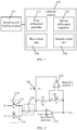
- FIG. 1 is a schematic structural diagram of a correlated double sampling integrating circuit according to the first embodiment of the present invention.
- the correlated double sampling integrating circuit includes: a sampling and holding module 101 and a feedback module 102.
- the feedback module 102 includes a first differential amplifier 112, a second differential amplifier 122, a first switch unit 142 and a second switch unit 132.
- the first switch unit 142 and the second switch unit 132 may be configured to have inverse ON states.
- the second differential amplifier 122 and the first switch unit 142 may are configured to form a first feedback loop with an energy storage unit (not shown in the drawings), and the first differential amplifier 112 and the second differential amplifier 122 may are configured to form a second feedback loop with the energy storage unit, to control node signals generated by the energy storage unit at a resetting stage.
- the energy storage unit is configured to form a third feedback loop with the first differential amplifier 112 to control node signals generated by the energy storage unit at an integrating stage.
- the correlated double sampling integrating circuit may enable the node signals at the integrating stage to be consistent with the node signals at the resetting stage.
- the correlated double sampling integrating circuit eliminates the noise caused by 1/f noise of the operational amplifier and noise caused by mismatch voltages, and prevents or weakens output jump of the correlated double sampling integrating circuit caused by the increase of the count of integrations.
- FIG. 2 is a specific schematic structural diagram of a correlated double sampling integrating circuit according to the second embodiment of the present invention.
- the first differential amplifier 112 is also marked as an operational amplifier 1
- the second differential amplifier 122 is also marked as an operational amplifier 2, wherein:
- the sampling and holding module includes a sampling unit 111 and a holding unit 121.
- the sampling unit 111 is configured to respectively sample different input signals (VI and V2).
- the holding unit 121 (for example, a holding capacitor Ci) is configured to hold the sampled input signals.
- One terminal of the holding unit 121 is connected to the sampling unit 111, and the other terminal of the holding unit 121 is respectively connected to one terminal of the first switch unit 142 (also marked as S4), one terminal of an energy storage unit 103 (for example, the energy storage capacitor Cf in the drawings) and an inverting terminal of the first differential amplifier 112.
- An output terminal of the first differential amplifier 112 and the other terminal of the energy storage unit 103 are respectively connected to a non-inverting terminal and an inverting terminal of the second differential amplifier 122.
- the second switch unit 132 (also marked as S3) is configured to bridge the non-inverting terminal and the inverting terminal of the second differential amplifier 122.
- the other terminal of the first switch unit 142 is connected to an output terminal of the second differential amplifier 122.
- specifically inverse ON states of the first switch unit 142 and the second switch unit 132 may be respectively controlled by two non-overlap clock signals ⁇ 1 and ⁇ 2.
- the sampling and holding module 101 specifically includes a third switch unit 131 (also marked as S1) and a fourth switch unit 141 (also marked as S2).
- the third switch unit 131 and the fourth switch unit 141 may be configured to have inverse ON states.
- the inverse ON states of the third switch unit 131 and the fourth switch unit 141 may also be controlled by the above two non-overlap clock signals ⁇ 1 and ⁇ 2. That is, the two non-overlap clock signals ⁇ 1 and ⁇ 2 respectively control the third switch unit 131 and the fourth switch unit 141 to make a turn-on or turn-off action, such that the third switch unit 131 and the fourth switch unit 141 have the inverse ON states to sample the input signal V1.
- the first switch unit 142 and the third switch unit 131 are synchronously turned on, the second switch unit 132 and the fourth switch unit 141 are synchronously turned off, such that the second differential amplifier 122 and the first switch unit 142 are configured to form a first feedback loop with the energy storage unit 103, and the first differential amplifier 112 and the second differential amplifier 122 are configured to form a second feedback loop with the energy storage unit 103, to control the node signals generated by the energy storage unit 103 at the resetting stage.
- the two non-overlap clock signals ⁇ 1 and ⁇ 2 respectively control the third switch unit 131 and the fourth switch unit 141 to make a turn-on or turn-off action such that the third switch unit 131 and the fourth switch unit 141 have different ON states to sample the input signal V2.
- the first switch unit 142 and the third switch unit 131 are synchronously turned off, and the second switch unit 132 and the fourth switch unit 141 are synchronously turned on, such that the energy storage unit 103 is configured to form a third feedback loop with the first differential amplifier 112 to control the node signals generated by the energy storage unit 103 at the integrating stage, such that the node signals at the integrating stage is consistent with the node signals at the resetting stage.
- a stage where the clock signal ⁇ 1 is high and the clock signal ⁇ 2 is low is defined as the resetting stage, and a stage where the clock signal ⁇ 1 is low and the clock signal ⁇ 2 is high is defined as the integrating stage.
- the 1/f noise of the operational amplifier and the noise caused by mismatch voltages and the like are not considered, and in another aspect assume that a gain of the second differential amplifier 122 is 1, an initial charge of the energy storage capacitor is 0 and a common-mode voltage Vcm is 0; and correspondingly, the correlated double sampling integrating circuit in this embodiment operates as follows:
- the clock signal ⁇ 1 is high and the clock signal ⁇ 2 is low, such that the third switch unit 131 and the first switch unit 142 are both turned on, and the fourth switch unit 141 and the second switch unit 132 are both turned off.
- two terminals of the energy storage unit 103 are bridged between the inverting terminal and the output terminal of the second differential amplifier 122, such that the first negative feedback loop is formed.
- the charges injected into a node 2 may be all absorbed by the second differential amplifier 122.
- the third switch S3 is configured to be turned off, the charges injected into the node 2 may not be transferred to the energy storage unit 103, such that the charges in the energy storage unit 103 are held.
- the output Vout of the integrating circuit may not be affected.
- the voltage at the node 2 is equal to the common-mode voltage Vcm and is 0 V. Therefore, the voltage at a negative electrode sheet of the energy storage unit 103 is 0, the voltage at a negative electrode sheet of the holding unit 121 is also 0, and the voltage at a positive electrode sheet of the holding unit 121 is the voltage of the output signal V1.
- the fourth switch unit 141 and the second switch unit 132 are both turned on, and the third switch unit 131 and the first switch unit 142 are both turned off.
- the second differential amplifier 122 is removed from the loop, the two terminals of the energy storage unit 103 are respectively bridged between the inverting terminal and the output terminal of the first differential amplifier 112, such that a third negative feedback loop is formed.
- the charges injected into the node 2 may be absorbed by the energy storage unit 103.
- the input signal V1 at the positive electrode sheet of the holding unit 121 is changed to the input signal V2. Therefore, the output Vout of the integrating circuit may be calculated according to formula (1).
- V out V 1 ⁇ V 2 C i C f ,
- the charges in the energy capacitor Cf are not affected by the changes of the voltage at the positive electrode sheet of the holding unit 121. Therefore, the voltage at a node 1B at this time is (V1-V2) Ci/Cf. Since the second differential amplifier 122 is virtually shorted, the voltages at the nodes 1B and 1A are consistent, which are both equal to the common-mode voltage Vcm. Therefore, the output Vout of the integrating circuit is equal to the output Vout of the integrating circuit at the first integrating stage, that is, the output Vout of the integrating circuit is determined according to formula (1).
- V out V 1 ⁇ V 2 + ⁇ V T ⁇ ⁇ V T 2 C i C f where T is a clock cycle.
- FIG. 3 is a schematic structural diagram of a correlated double sampling integrating circuit according to the third embodiment of the present invention.
- FIG. 4 is a specific schematic structural diagram of a correlated double sampling integrating circuit according to the fourth embodiment of the present invention.
- the correlated double sampling integrating circuit includes: a feedback module 102 and a sampling and holding module 101, wherein:
- the feedback module 102 includes a single-input and single-output amplifier 152, a second differential amplifier 122, a first switch unit 142 and a second switch unit 132.
- the first switch unit 142 is configured to be turned on and the second switch unit 132 is configured to be turned off, such that the second differential amplifier 122 is configured to form a fourth feedback loop with the first switch unit 142, and the single-input and single-output amplifier 152 and the second differential amplifier 122 are configured to form a fifth feedback loop with the energy storage unit 103, to control the node signals generated by the energy storage unit 103 at the resetting stage.
- first switch unit 142 is configured to be turned off and the second switch unit 132 is configured to be turned on, such that the energy storage unit 103 is configured to form a sixth feedback loop with the single-input and single-output amplifier 152 to control node signals generated by the energy storage unit 103 at the integrating stage.
- ON and OFF states of the first switch unit 142 and the second switch unit 132 may be respectively controlled by the two non-overlap clock signals ⁇ 1 and ⁇ 2.
- the sampling and holding module 101 also includes a sampling unit 111 and a holding unit 121.
- the sampling unit 111 is configured to sample the different input signals (VI and V2)
- the holding unit 121 is configured to hold the sampled input signals.
- one terminal of the holding unit 121 is respectively connected to the sampling unit 111
- the other terminal of the holding unit 121 is respectively connected to one terminal of the first switch unit 142, an input terminal of the single-input and single-output amplifier 152 and an inverting terminal of the second differential amplifier 122.
- An output terminal of the single-input and single-output amplifier 152 is connected to one terminal (the positive electrode sheet terminal) of the energy storage unit 103, and the other terminal (the negative electrode sheet terminal) of the energy storage unit 103 is respectively connected to a non-inverting terminal of the second differential amplifier 122.
- the second switch unit 132 is configured to bridge the non-inverting terminal and the inverting terminal of the second differential amplifier 122, and the other terminal of the first switch unit 142 is connected to an output terminal of the second differential amplifier 122.
- the sampling and holding module 101 includes a third switch unit 131 and a fourth switch unit 141.
- the third switch unit 131 and the fourth switch unit 141 are configured to switch on or switch off under control of the two non-overlap signals ⁇ 1 and ⁇ 2 to sample the input signal V1.
- the first switch unit 142 and the third switch unit 131 are configured to be simultaneously turned on and off, and the second switch unit 132 and the fourth switch unit 142 are configured to be simultaneously turned off, such that the second differential amplifier 122 forms the fourth feedback loop with the first switch unit 142, and the single-input and single-output amplifier 152 and the second differential amplifier 122 form the fifth feedback loop with the energy storage unit 103, to control the node signals generated by the energy storage unit 103 at the resetting stage.
- the third switch unit 131 and the fourth switch unit 141 are further configured to sample the input signal V2 under control of the two non-overlap clock signals ⁇ 1 and ⁇ 2.
- the first switch unit 142 and the third switch unit 131 are configured to be simultaneously turned off, and the second switch unit 132 and the fourth switch unit 141 are configured to be simultaneously turned on, such that the energy storage unit 103 forms the sixth feedback loop with the single-input and single-output amplifier 152 to control the node signals generated by the energy storage unit 103 at the integrating stage.
- the second switch unit 132 arranged between the negative electrode sheet of the energy storage capacitor and the inverting terminal of the single-input and single-output amplifier 152 results in two nodes: a node 2A and a node 2B. It is equivalent that two nodes are inserted. Since the second differential amplifier 122 is virtually shorted, the voltages (the node signals) at the nodes 2A and 2B are both equal to the common-mode voltage Vcm, which are substantially maintained to be constant, such that the node signals at the nodes 2A and 2B constantly vary with the variation of the count of integrations. In this way, the noise caused by 1/f noise of the operational amplifier and noise caused by mismatch voltage are eliminated, and output jump of the correlated double sampling integrating circuit caused by the increase of the count of integrations are prevented or weakened.
- the above first differential amplifier is replaced with the single-input and single-output amplifier 152, and a common-mode voltage Vcm is generated inside the single-input and single-output amplifier 152, such that power consumption and noise are further reduced.
- the turn-on or turn-off action of the second switch unit 132 at the integrating stage is inverse to the turn-on or turn-off action of the second switch unit 132 at the holding stage, such that the charge injection effects are inverse.
- the energy storage capacitor since the inject effects within a cycle may cause differences to the charges therein, the energy storage capacitor in each cycle may have some remaining charges. In an ideal condition, the energy storage capacitor has no remaining charges within each cycle. However, since the amounts of the remaining charges within various cycles are almost the same or no charges remain, the charge inject effects may not affect linearity of the integrating circuit.
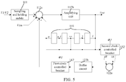
- FIG. 5 is a block diagram of a correlated double sampling integrating circuit according to the fifth embodiment of the present invention.
- the correlated double sampling integrating circuit includes: a sampling and holding module 101 and a feedback module 102.
- the feedback module 102 includes: a first adder 112a, an amplifying unit 112b, a plurality of energy storage units 103, a second clock-controlled breaker 132', a second adder 122a, a buffer circuit 122b and a first clock-controlled breaker 142'.
- a combination of the first adder 112a and the amplifying unit 112b is equivalent to the first differential amplifier.
- the second clock-controlled breaker 132' is equivalent to the second switch unit 132.
- the first clock-controlled breaker 142' is equivalent to the first switch unit 142.
- a combination of the second adder 122a and the buffer circuit 122b is equivalent to the second differential amplifier 122.
- a node iB for example, a node 2b
- a node iA for example, a node 2A
- the cascaded node 3 is split into a node 3B and a node 3A via the second clock-controlled breaker 132', such that by means of the feedback module 102, the node signals at the nodes iB and iA may be controlled to not vary with the variation of the count of integrations. In this way, the noise caused by 1/f noise of the operational amplifier and noise caused by mismatch voltage are eliminated, and output jump of the correlated double sampling integrating circuit caused by the increase of the count of integrations are prevented or weakened.
- the third switch unit (not shown in the drawings) and the first clock-controlled breaker 142' are turned on, the fourth switch unit (not shown in the drawings) and the second clock-controlled breaker 132' are turned off.
- two terminals of the energy storage unit 103 are bridged between an inverting terminal and an amplification output terminal of the first adder 112a, such that the first negative feedback loop is formed; and the first adder 112a, the amplifying unit 112b, the adder 122a and the energy storage unit 103 form the second negative feedback loop.
- the fourth switch unit (not shown in the drawings) and the second clock-controlled breaker 132' are turned on, and the third switch unit (not shown in the drawings) and the first clock-controlled breaker 142' are turned off.
- the second adder 122a is removed from the loop, and the two terminals of the energy storage unit 103 are respectively bridged between an inverting terminal and a non-inverting terminal of the second adder 122a, such that the above third negative feedback loop is formed.
- circuit modules or circuit units in the above embodiments may be individual devices or may be combinations of a plurality of devices, as long as the above functions may be implemented thereby.
- the apparatus according to the embodiments of the present application may be practiced by a computer program.
- a person skilled in the art should understand the above division of units and modules is only an exemplary one, and if the apparatus is divided into other units or modules or not divided, the technical solution shall also fall within the protection scope of the present application as long as the information object has the above functions.
- the embodiments of the present application may be described to illustrate methods, apparatuses (devices), or computer program products. Therefore, hardware embodiments, software embodiments, or hardware-plus-software embodiments may be used to illustrate the present application.
- the present application may further employ a computer program product which may be implemented by at least one non-transitory computer-readable storage medium with an executable program code stored thereon.
- the non-transitory computer-readable storage medium comprises but not limited to a disk memory, a CD-ROM, and an optical memory.
- the present invention is described based on the flowcharts and/or block diagrams of the method, apparatus (device), and computer program product. It should be understood that each process and/or block in the flowcharts and/or block diagrams, and any combination of the processes and/or blocks in the flowcharts and/or block diagrams may be implemented using computer program instructions. These computer program instructions may be issued to a computer, a dedicated computer, an embedded processor, or processors of other programmable data processing device to generate a machine, which enables the computer or the processors of other programmable data processing devices to execute the instructions to implement an apparatus for implementing specific functions in at least one process in the flowcharts and/or at least one block in the block diagrams.
- These computer program instructions may also be stored a non-transitory computer-readable memory capable of causing a computer or other programmable data processing devices to work in a specific mode, such that the instructions stored on the non-transitory computer-readable memory implement a product comprising an instruction apparatus, where the instruction apparatus implements specific functions in at least one process in the flowcharts and/or at least one block in the block diagrams.
- These computer program instructions may also be stored on a computer or other programmable data processing devices, such that the computer or the other programmable data processing devices execute a series of operations or steps to implement processing of the computer.
- the instructions when executed on the computer or the other programmable data processing devices, implement the specific functions in at least one process in the flowcharts and/or at least one block in the block diagrams.
Landscapes
- Engineering & Computer Science (AREA)
- Power Engineering (AREA)
- Theoretical Computer Science (AREA)
- Amplifiers (AREA)
- Transforming Light Signals Into Electric Signals (AREA)
Abstract
Description
- Embodiments of the present invention relate to the technical field of circuits, and in particular, relate to a correlated double sampling integrating circuit.
- To reduce the 1/f noise of the operational amplifier and the noise caused by mismatch voltages and the like in an integrating circuit, generally the correlated double sampling technology may be introduced. Specifically, different input signals are successively sampled twice, and the input signals upon the twice samplings are subjected to an analogous subtraction, to eliminate the 1/f noise of the operational amplifier and the noise caused by mismatch voltages and the like. In this way, real signal levels are obtained.
- An exemplary correlated double sampling integrating circuit includes: a sampling circuit, an energy storage capacitor and an amplifier. The sampling circuit performs time-division based sampling under control of two non-overlap clock signals Φ1 and Φ2. When the clock signal Φ1 is high and the clock signal Φ2 is low, a positive electrode sheet of the energy storage capacitor Ci samples an input signal V1, and meanwhile a negative electrode sheet thereof may sample the 1/f noise of the operational amplifier and the noise caused by mismatch voltages and the like. When the clock signal Φ1 is low and the clock signal Φ2 is high, the positive electrode sheet of the energy storage capacitor Ci samples an input signal V2, and meanwhile the negative electrode sheet thereof may sample the 1/f noise of the operational amplifier and the noise caused by mismatch voltages and the like. If at two contiguous phases, the /f noise of the operational amplifier and the mismatch voltages substantially remain unchanged, with respect to two adjacent sampling time periods, the variation amount of the output voltage of the amplifier is not affected by the 1/f noise and the mismatch voltages, such that /f noise of the operational amplifier and the noise caused by mismatch voltages and the like are eliminated.
- However, in the above exemplary correlated double sampling integrating circuit, at the moment the clock signal Φ1 changes from a low level to a high level, the output of the amplifier may transition from an output value when the clock signal Φ2 is a high level to a common-mode voltage Vcm. Likewise, at the moment the clock signal Φ2 changes from a low level to a high level, the output of the amplifier may transition from the common-mode voltage Vcm to a sum of the output value of the original stage of the clock signal Φ2 and an integration value. Consequently, the output jump of the correlated double sampling integrating circuit become greater and greater as the count of integrations increases.
- Embodiments of the present invention are intended to provide a correlated double sampling integrating circuit to at least solve the above problem in the prior art.
- To achieve the objective, embodiments of the present invention provide a correlated double sampling integrating circuit. The correlated double sampling integrating circuit includes: a sampling and holding module, an energy storage unit and a feedback module; where the sampling and holding module is configured to perform sampling and holding for different input signals, the energy storage unit is configured to store charges corresponding to the input signals upon the sampling and holding to generate node signals, and the feedback module is configured to form a negative feedback loop with the energy storage unit to a control node signal at an integrating stage to be consistent with a node signal at a resetting stage and prevent output jump of the correlated double sampling integrating circuit.
- Optionally, in an embodiment of the present invention, the feedback module includes: a differential amplifier and a switch unit, configured to respectively form different negative feedback loops with the energy storage unit to respectively control the node signals generated by the energy storage unit at the integrating stage and the resetting stage, such that the node signal at the integrating stage is consistent with the node signal at the resetting stage.
- Optionally, in an embodiment of the present invention, the feedback module includes a first differential amplifier, a second differential amplifier, a first switch unit and a second switch unit; where the first switch unit is configured to be turned on and the second switch unit is configured to be turned off, such that the second differential amplifier and the first switch unit are configured to form a first feedback loop with the energy storage unit, and the first differential amplifier and the second differential amplifier are configured to form a second feedback loop with the energy storage unit, to control the node signal generated by the energy storage unit at the resetting stage.
- Optionally, in an embodiment of the present invention, the feedback module includes a first differential amplifier, a second differential amplifier, a first switch unit and a second switch unit; where the first switch unit is configured to be turned off and the second switch unit is configured to be turned on, such that the energy storage unit is configured to form a third feedback loop with the first differential amplifier to control the node signal generated by the energy storage unit at the integrating stage.
- Optionally, in an embodiment of the present invention, the sampling and holding module includes a sampling unit and a holding unit; where the sampling unit is configured to sample the different input signals, and the holding unit is configured to hold the sampled input signals; one terminal of the holding unit is connected to the sampling unit, and the other terminal of the holding unit is respectively connected to one terminal of the first switch unit, one terminal of the energy storage unit and an inverting terminal of the first differential amplifier; and an output terminal of the first differential amplifier and the other terminal of the energy storage unit are respectively connected to a non-inverting terminal and an inverting terminal of the second differential amplifier, the second switch unit is configured to bridge the non-inverting terminal and the inverting terminal of the second differential amplifier, and the other terminal of the first switch unit is connected to an output terminal of the second differential amplifier.
- Optionally, in an embodiment of the present invention, ON/OFF of the first switch unit and the second switch unit are respectively controlled by two non-overlap clock signals.
- Optionally, in an embodiment of the present invention, the sampling and holding module includes a third switch unit and a fourth switch unit, and is further configured to sample the different input signals under control of the two non-overlap clock signals; where the first switch unit and the third switch unit are configured to be simultaneously turned on, and the second switch unit and the fourth switch unit are configured to be simultaneously turned off, such that the second differential amplifier and the first switch unit form the first feedback loop with the energy storage unit, and the first differential amplifier and the second differential amplifier form the second feedback loop with the energy storage unit.
- Optionally, in an embodiment of the present invention, the sampling and holding module includes a third switch unit and a fourth switch unit, and is further configured to sample the different input signals under control of the two non-overlap clock signals; where the first switch unit and the third switch unit are configured to be simultaneously turned off, and the second switch unit and the fourth switch unit are configured to be simultaneously turned on, such that the energy storage unit first the third feedback loop with the first differential amplifier to control the node signal generated by the energy storage unit at the integrating stage.
- Optionally, in an embodiment of the present invention, the feedback module includes a single-input and single-output amplifier, a second differential amplifier, a first switch unit and a second switch unit; where the first switch unit is configured to be turned on and the second switch unit is configured to be turned off, such that the second differential amplifier is configured to form a fourth feedback loop with the first switch unit, and the single-input and single-output amplifier and the second differential amplifier are configured to form a fifth feedback loop with the energy storage unit, to control the node signal generated by the energy storage unit at the resetting stage.
- Optionally, in an embodiment of the present invention, the feedback module includes a single-input and single-output amplifier, a second differential amplifier, a first switch unit and a second switch unit; where the first switch unit is configured to be turned off and the second switch unit is configured to be turned on, such that the energy storage unit is configured to form a sixth feedback loop with the single-input and single-output amplifier to control the node signals generated by the energy storage unit at the integrating stage.
- Optionally, in an embodiment of the present invention, the sampling and holding module includes a sampling unit and a holding unit; where the sampling unit is configured to sample the different input signals, and the holding unit is configured to hold the sampled input signals; one terminal of the holding unit is connected to the sampling unit, and the other terminal of the holding unit is respectively connected to one terminal of the first switch unit, an input terminal of the single-input and single-output amplifier and an inverting terminal of the second differential amplifier; an output terminal of the single-input and single-output amplifier is connected to one terminal of the energy storage unit, and the other terminal of the energy storage unit is respectively connected to a non-inverting terminal of the second differential amplifier, the second switch unit is configured to bridge the non-inverting terminal and an inverting terminal of the second differential amplifier, and the other terminal of the first switch unit is connected to an output terminal of the second differential amplifier.
- Optionally, in an embodiment of the present invention, ON/OFF of the first switch unit and the second switch unit are respectively controlled by two non-overlap clock signals.
- Optionally, in an embodiment of the present invention, the sampling and holding module includes a third switch unit and a fourth switch unit, and is further configured to sample the different input signals under control of the two non-overlap clock signals; where the first switch unit and the third switch unit are configured to be simultaneously turned on, and the second switch unit and the fourth switch unit are configured to be simultaneously turned off, such that the second differential amplifier forms the fourth feedback loop with the first switch unit, and the single-input and single-output amplifier and the second differential amplifier form the fifth feedback loop with the energy storage unit, to control the node signal generated by the energy storage unit at the resetting stage.
- Optionally, in an embodiment of the present invention, the sampling and holding module includes a third switch unit and a fourth switch unit and is further configured to sample the different input signals under control of the two non-overlap clock signals; the first switch unit and the third switch unit are configured to be simultaneously turned off, and the second switch unit and the fourth switch unit are configured to be simultaneously turned on, such that the energy storage unit forms the sixth feedback loop with the single-input and single-output amplifier to control the node signals generated by the energy storage unit at the integrating stage.
- Optionally, in an embodiment of the present invention, the second switch unit is a second clock-controlled breaker; and/or the first switch unit is a first clock-controlled breaker.
- According to embodiments of the present invention, the correlated double sampling integrating circuit mainly includes: a sampling and holding module, an energy storage unit and a feedback module; where the sampling and holding module is configured to perform sampling and holding for different input signals, the energy storage unit is configured to store charges corresponding to the input signals upon the sampling and holding to generate node signals (for example, node voltages), and the feedback module is configured to form a negative feedback loop with the energy storage unit to control a node signal at an integrating stage to be consistent with a node signal at a resetting stage and prevent output jump of the correlated double sampling integrating circuit. The feedback module may include: a differential amplifier and a switch unit, configured to respectively form different negative feedback loops with the energy storage unit to respectively control the node signals generated by the energy storage unit at the integrating stage and the resetting stage, such that the node signals at the integrating stage is consistent with the node signal at the resetting stage. Therefore, the correlated double sampling integrating circuit eliminates the noise caused by 1/f noise of the operational amplifier and noise caused by mismatch voltage, and prevents or weakens output jump of the correlated double sampling integrating circuit caused by the increase of the count of integrations.
-
-
FIG. 1 is a schematic structural diagram of a correlated double sampling integrating circuit according to the first embodiment of the present invention; -
FIG. 2 is a specific schematic structural diagram of a correlated double sampling integrating circuit according to the second embodiment of the present invention; -
FIG. 3 is a schematic structural diagram of a correlated double sampling integrating circuit according to the third embodiment of the present invention; -
FIG. 4 is a specific schematic structural diagram of a correlated double sampling integrating circuit according to the fourth embodiment of the present invention; and -
FIG. 5 is a block diagram of a correlated double sampling integrating circuit according to the fifth embodiment of the present invention. - Practice of the present application is described in detail with reference to drawings and specific embodiments, such that the practice of addressing the technical problem using the technical means according to the present application and achieving the technical effects may be better understood and conducted.
- A correlated double sampling integrating circuit according to the embodiments of the present invention mainly includes: a sampling and holding module, an energy storage unit and a feedback module; where the sampling and holding module is configured to perform sampling and holding for different input signals, the energy storage unit is configured to store charges corresponding to the input signals upon the sampling and holding to generate node signals (for example, node voltages), and the feedback module is configured to form a negative feedback loop with the energy storage unit to control node signals at an integrating stage to be consistent with node signals at a resetting stage and prevent output jump of the correlated double sampling integrating circuit. The feedback module may include: a differential amplifier and a switch unit, configured to respectively form different negative feedback loops with the energy storage unit to respectively control the node signals generated by the energy storage unit at the integrating stage and the resetting stage, such that the node signals at the integrating stage is consistent with the node signal at the resetting stage. Therefore, the correlated double sampling integrating circuit eliminates the noise caused by 1/f noise of the operational amplifier and noise caused by mismatch voltages, and prevents or weakens output jump of the correlated double sampling integrating circuit caused by the increase of the count of integrations.
- In the embodiments hereinafter of the present invention, the above correlated sampling circuit is illustratively interpreted with reference to an exemplary specific circuit.
-
FIG. 1 is a schematic structural diagram of a correlated double sampling integrating circuit according to the first embodiment of the present invention. As illustrated inFIG. 1 , the correlated double sampling integrating circuit includes: a sampling andholding module 101 and afeedback module 102. Thefeedback module 102 includes a firstdifferential amplifier 112, a seconddifferential amplifier 122, afirst switch unit 142 and asecond switch unit 132. Thefirst switch unit 142 and thesecond switch unit 132 may be configured to have inverse ON states. For example, when thefirst switch unit 142 is configured to be turned on and thesecond switch unit 132 is configured to be turned off, the seconddifferential amplifier 122 and thefirst switch unit 142 may are configured to form a first feedback loop with an energy storage unit (not shown in the drawings), and the firstdifferential amplifier 112 and the seconddifferential amplifier 122 may are configured to form a second feedback loop with the energy storage unit, to control node signals generated by the energy storage unit at a resetting stage. When thefirst switch unit 142 is configured to be turned off and thesecond switch unit 132 is configured to be turned on, the energy storage unit is configured to form a third feedback loop with the firstdifferential amplifier 112 to control node signals generated by the energy storage unit at an integrating stage. Therefore, the correlated double sampling integrating circuit according to this embodiment may enable the node signals at the integrating stage to be consistent with the node signals at the resetting stage. The correlated double sampling integrating circuit eliminates the noise caused by 1/f noise of the operational amplifier and noise caused by mismatch voltages, and prevents or weakens output jump of the correlated double sampling integrating circuit caused by the increase of the count of integrations. -
FIG. 2 is a specific schematic structural diagram of a correlated double sampling integrating circuit according to the second embodiment of the present invention. As illustrated inFIG. 2 , in this embodiment, the firstdifferential amplifier 112 is also marked as anoperational amplifier 1, and the seconddifferential amplifier 122 is also marked as anoperational amplifier 2, wherein: - The sampling and holding module includes a
sampling unit 111 and aholding unit 121. Thesampling unit 111 is configured to respectively sample different input signals (VI and V2). The holding unit 121 (for example, a holding capacitor Ci) is configured to hold the sampled input signals. One terminal of theholding unit 121 is connected to thesampling unit 111, and the other terminal of theholding unit 121 is respectively connected to one terminal of the first switch unit 142 (also marked as S4), one terminal of an energy storage unit 103 (for example, the energy storage capacitor Cf in the drawings) and an inverting terminal of the firstdifferential amplifier 112. An output terminal of the firstdifferential amplifier 112 and the other terminal of theenergy storage unit 103 are respectively connected to a non-inverting terminal and an inverting terminal of the seconddifferential amplifier 122. The second switch unit 132 (also marked as S3) is configured to bridge the non-inverting terminal and the inverting terminal of the seconddifferential amplifier 122. The other terminal of thefirst switch unit 142 is connected to an output terminal of the seconddifferential amplifier 122. - In this embodiment, specifically inverse ON states of the
first switch unit 142 and thesecond switch unit 132 may be respectively controlled by two non-overlap clock signals Φ1 and Φ2. - Further, in this embodiment, the sampling and holding
module 101 specifically includes a third switch unit 131 (also marked as S1) and a fourth switch unit 141 (also marked as S2). Thethird switch unit 131 and thefourth switch unit 141 may be configured to have inverse ON states. Specifically, for example, the inverse ON states of thethird switch unit 131 and thefourth switch unit 141 may also be controlled by the above two non-overlap clock signals Φ1 and Φ2. That is, the two non-overlap clock signals Φ1 and Φ2 respectively control thethird switch unit 131 and thefourth switch unit 141 to make a turn-on or turn-off action, such that thethird switch unit 131 and thefourth switch unit 141 have the inverse ON states to sample the input signal V1. Meanwhile, thefirst switch unit 142 and thethird switch unit 131 are synchronously turned on, thesecond switch unit 132 and thefourth switch unit 141 are synchronously turned off, such that the seconddifferential amplifier 122 and thefirst switch unit 142 are configured to form a first feedback loop with theenergy storage unit 103, and the firstdifferential amplifier 112 and the seconddifferential amplifier 122 are configured to form a second feedback loop with theenergy storage unit 103, to control the node signals generated by theenergy storage unit 103 at the resetting stage. - Further, the two non-overlap clock signals Φ1 and Φ2 respectively control the
third switch unit 131 and thefourth switch unit 141 to make a turn-on or turn-off action such that thethird switch unit 131 and thefourth switch unit 141 have different ON states to sample the input signal V2. Meanwhile, thefirst switch unit 142 and thethird switch unit 131 are synchronously turned off, and thesecond switch unit 132 and thefourth switch unit 141 are synchronously turned on, such that theenergy storage unit 103 is configured to form a third feedback loop with the firstdifferential amplifier 112 to control the node signals generated by theenergy storage unit 103 at the integrating stage, such that the node signals at the integrating stage is consistent with the node signals at the resetting stage. - In an optional embodiment, for example, a stage where the clock signal Φ1 is high and the clock signal Φ2 is low is defined as the resetting stage, and a stage where the clock signal Φ1 is low and the clock signal Φ2 is high is defined as the integrating stage. In one aspect assume that the 1/f noise of the operational amplifier and the noise caused by mismatch voltages and the like are not considered, and in another aspect assume that a gain of the second
differential amplifier 122 is 1, an initial charge of the energy storage capacitor is 0 and a common-mode voltage Vcm is 0; and correspondingly, the correlated double sampling integrating circuit in this embodiment operates as follows: - At the first resetting stage, the clock signal Φ1 is high and the clock signal Φ2 is low, such that the
third switch unit 131 and thefirst switch unit 142 are both turned on, and thefourth switch unit 141 and thesecond switch unit 132 are both turned off. In this case, two terminals of theenergy storage unit 103 are bridged between the inverting terminal and the output terminal of the seconddifferential amplifier 122, such that the first negative feedback loop is formed. In this case, the charges injected into anode 2 may be all absorbed by the seconddifferential amplifier 122. However, since the third switch S3 is configured to be turned off, the charges injected into thenode 2 may not be transferred to theenergy storage unit 103, such that the charges in theenergy storage unit 103 are held. That is, regardless of how the voltage at a positive electrode sheet of the holdingunit 121 changes, the output Vout of the integrating circuit may not be affected. In addition, since the firstdifferential amplifier 112 and the seconddifferential amplifier 122 form the second negative feedback loop with theenergy storage unit 103, and the seconddifferential amplifier 122 is in a virtually shorted state, the voltage at thenode 2 is equal to the common-mode voltage Vcm and is 0 V. Therefore, the voltage at a negative electrode sheet of theenergy storage unit 103 is 0, the voltage at a negative electrode sheet of the holdingunit 121 is also 0, and the voltage at a positive electrode sheet of the holdingunit 121 is the voltage of the output signal V1. - At the first integrating stage, the
fourth switch unit 141 and thesecond switch unit 132 are both turned on, and thethird switch unit 131 and thefirst switch unit 142 are both turned off. In this case, the seconddifferential amplifier 122 is removed from the loop, the two terminals of theenergy storage unit 103 are respectively bridged between the inverting terminal and the output terminal of the firstdifferential amplifier 112, such that a third negative feedback loop is formed. In this case, the charges injected into thenode 2 may be absorbed by theenergy storage unit 103. In this case, the input signal V1 at the positive electrode sheet of the holdingunit 121 is changed to the input signal V2. Therefore, the output Vout of the integrating circuit may be calculated according to formula (1).
- At a second resetting stage, similar to the first resetting stage, the charges in the energy capacitor Cf are not affected by the changes of the voltage at the positive electrode sheet of the holding
unit 121. Therefore, the voltage at a node 1B at this time is (V1-V2) Ci/Cf. Since the seconddifferential amplifier 122 is virtually shorted, the voltages at the nodes 1B and 1A are consistent, which are both equal to the common-mode voltage Vcm. Therefore, the output Vout of the integrating circuit is equal to the output Vout of the integrating circuit at the first integrating stage, that is, the output Vout of the integrating circuit is determined according to formula (1). - Considering the 1/f noise of the operational amplifier and the noise δV(T) caused by mismatch voltages and the like, the noise δV(T) may be equivalent to the input signal. Referring to formula (1), upon the first integrating stage, the output Vout of the integrating circuit is given according to formula (2).

- According to formula (2), since a small interval is defined between the integrating stage and the resetting stage, it may be approximately considered that the noise δV(T) and the
noise 

-
FIG. 3 is a schematic structural diagram of a correlated double sampling integrating circuit according to the third embodiment of the present invention.FIG. 4 is a specific schematic structural diagram of a correlated double sampling integrating circuit according to the fourth embodiment of the present invention. As illustrated inFIG. 3 and FIG. 4 , in this embodiment, the correlated double sampling integrating circuit includes: afeedback module 102 and a sampling and holdingmodule 101, wherein: - The
feedback module 102 includes a single-input and single-output amplifier 152, a seconddifferential amplifier 122, afirst switch unit 142 and asecond switch unit 132. Thefirst switch unit 142 is configured to be turned on and thesecond switch unit 132 is configured to be turned off, such that the seconddifferential amplifier 122 is configured to form a fourth feedback loop with thefirst switch unit 142, and the single-input and single-output amplifier 152 and the seconddifferential amplifier 122 are configured to form a fifth feedback loop with theenergy storage unit 103, to control the node signals generated by theenergy storage unit 103 at the resetting stage. Further, thefirst switch unit 142 is configured to be turned off and thesecond switch unit 132 is configured to be turned on, such that theenergy storage unit 103 is configured to form a sixth feedback loop with the single-input and single-output amplifier 152 to control node signals generated by theenergy storage unit 103 at the integrating stage. In this embodiment, ON and OFF states of thefirst switch unit 142 and thesecond switch unit 132 may be respectively controlled by the two non-overlap clock signals Φ1 and Φ2. - The sampling and holding
module 101 also includes asampling unit 111 and a holdingunit 121. Thesampling unit 111 is configured to sample the different input signals (VI and V2), and the holdingunit 121 is configured to hold the sampled input signals. Specifically, one terminal of the holdingunit 121 is respectively connected to thesampling unit 111, and the other terminal of the holdingunit 121 is respectively connected to one terminal of thefirst switch unit 142, an input terminal of the single-input and single-output amplifier 152 and an inverting terminal of the seconddifferential amplifier 122. An output terminal of the single-input and single-output amplifier 152 is connected to one terminal (the positive electrode sheet terminal) of theenergy storage unit 103, and the other terminal (the negative electrode sheet terminal) of theenergy storage unit 103 is respectively connected to a non-inverting terminal of the seconddifferential amplifier 122. Thesecond switch unit 132 is configured to bridge the non-inverting terminal and the inverting terminal of the seconddifferential amplifier 122, and the other terminal of thefirst switch unit 142 is connected to an output terminal of the seconddifferential amplifier 122. - Specifically, the sampling and holding
module 101 includes athird switch unit 131 and afourth switch unit 141. Thethird switch unit 131 and thefourth switch unit 141 are configured to switch on or switch off under control of the two non-overlap signals Φ1 and Φ2 to sample the input signal V1. Meanwhile, thefirst switch unit 142 and thethird switch unit 131 are configured to be simultaneously turned on and off, and thesecond switch unit 132 and thefourth switch unit 142 are configured to be simultaneously turned off, such that the seconddifferential amplifier 122 forms the fourth feedback loop with thefirst switch unit 142, and the single-input and single-output amplifier 152 and the seconddifferential amplifier 122 form the fifth feedback loop with theenergy storage unit 103, to control the node signals generated by theenergy storage unit 103 at the resetting stage. Further, thethird switch unit 131 and thefourth switch unit 141 are further configured to sample the input signal V2 under control of the two non-overlap clock signals Φ1 and Φ2. Meanwhile, thefirst switch unit 142 and thethird switch unit 131 are configured to be simultaneously turned off, and thesecond switch unit 132 and thefourth switch unit 141 are configured to be simultaneously turned on, such that theenergy storage unit 103 forms the sixth feedback loop with the single-input and single-output amplifier 152 to control the node signals generated by theenergy storage unit 103 at the integrating stage. - In this embodiment, the
second switch unit 132 arranged between the negative electrode sheet of the energy storage capacitor and the inverting terminal of the single-input and single-output amplifier 152 results in two nodes: anode 2A and anode 2B. It is equivalent that two nodes are inserted. Since the seconddifferential amplifier 122 is virtually shorted, the voltages (the node signals) at thenodes nodes - In addition, different from the second embodiment as described above, the above first differential amplifier is replaced with the single-input and single-
output amplifier 152, and a common-mode voltage Vcm is generated inside the single-input and single-output amplifier 152, such that power consumption and noise are further reduced. - Still further, since the turn-on or turn-off action of the
second switch unit 132 at the integrating stage is inverse to the turn-on or turn-off action of thesecond switch unit 132 at the holding stage, such that the charge injection effects are inverse. With respect to the energy storage capacitor, since the inject effects within a cycle may cause differences to the charges therein, the energy storage capacitor in each cycle may have some remaining charges. In an ideal condition, the energy storage capacitor has no remaining charges within each cycle. However, since the amounts of the remaining charges within various cycles are almost the same or no charges remain, the charge inject effects may not affect linearity of the integrating circuit. -
FIG. 5 is a block diagram of a correlated double sampling integrating circuit according to the fifth embodiment of the present invention. As illustrated inFIG. 5 , the correlated double sampling integrating circuit includes: a sampling and holdingmodule 101 and afeedback module 102. Thefeedback module 102 includes: afirst adder 112a, an amplifyingunit 112b, a plurality ofenergy storage units 103, a second clock-controlled breaker 132', asecond adder 122a, abuffer circuit 122b and a first clock-controlled breaker 142'. A combination of thefirst adder 112a and the amplifyingunit 112b is equivalent to the first differential amplifier. The second clock-controlled breaker 132' is equivalent to thesecond switch unit 132. The first clock-controlled breaker 142' is equivalent to thefirst switch unit 142. A combination of thesecond adder 122a and thebuffer circuit 122b is equivalent to the seconddifferential amplifier 122. The second clock-controlled breaker 132' may be connected to an ith cascaded node (i=1, 2, ..., n) of any of the plurality ofenergy storage units 103, which is equivalent to splitting the cascaded node to which the second clock-controlled breaker 132' is connected into two nodes: a node iB (for example, a node 2b), and a node iA (for example, anode 2A). For example, as illustrated inFIG. 5 , if the second clock-controlled breaker 132' is connected to the cascadednode 3, it is signified that the cascadednode 3 is split into a node 3B and a node 3A via the second clock-controlled breaker 132', such that by means of thefeedback module 102, the node signals at the nodes iB and iA may be controlled to not vary with the variation of the count of integrations. In this way, the noise caused by 1/f noise of the operational amplifier and noise caused by mismatch voltage are eliminated, and output jump of the correlated double sampling integrating circuit caused by the increase of the count of integrations are prevented or weakened. - The operation process of the correlated double sampling integration as illustrated in
FIG. 5 is briefly described hereinafter. The detail process may be referenced to the above relevant disclosure of the embodiments. - At a first resetting stage, in the
sampling unit 111, the third switch unit (not shown in the drawings) and the first clock-controlled breaker 142' are turned on, the fourth switch unit (not shown in the drawings) and the second clock-controlled breaker 132' are turned off. In this case, two terminals of theenergy storage unit 103 are bridged between an inverting terminal and an amplification output terminal of thefirst adder 112a, such that the first negative feedback loop is formed; and thefirst adder 112a, the amplifyingunit 112b, theadder 122a and theenergy storage unit 103 form the second negative feedback loop. - At a first integrating stage, in the
sampling unit 111, the fourth switch unit (not shown in the drawings) and the second clock-controlled breaker 132' are turned on, and the third switch unit (not shown in the drawings) and the first clock-controlled breaker 142' are turned off. In this case, thesecond adder 122a is removed from the loop, and the two terminals of theenergy storage unit 103 are respectively bridged between an inverting terminal and a non-inverting terminal of thesecond adder 122a, such that the above third negative feedback loop is formed. - It should be noted that the circuit modules or circuit units in the above embodiments may be individual devices or may be combinations of a plurality of devices, as long as the above functions may be implemented thereby.
- The apparatus according to the embodiments of the present application may be practiced by a computer program. A person skilled in the art should understand the above division of units and modules is only an exemplary one, and if the apparatus is divided into other units or modules or not divided, the technical solution shall also fall within the protection scope of the present application as long as the information object has the above functions.
- A person skilled in the art shall understand that the embodiments of the present application may be described to illustrate methods, apparatuses (devices), or computer program products. Therefore, hardware embodiments, software embodiments, or hardware-plus-software embodiments may be used to illustrate the present application. In addition, the present application may further employ a computer program product which may be implemented by at least one non-transitory computer-readable storage medium with an executable program code stored thereon. The non-transitory computer-readable storage medium comprises but not limited to a disk memory, a CD-ROM, and an optical memory.
- The present invention is described based on the flowcharts and/or block diagrams of the method, apparatus (device), and computer program product. It should be understood that each process and/or block in the flowcharts and/or block diagrams, and any combination of the processes and/or blocks in the flowcharts and/or block diagrams may be implemented using computer program instructions. These computer program instructions may be issued to a computer, a dedicated computer, an embedded processor, or processors of other programmable data processing device to generate a machine, which enables the computer or the processors of other programmable data processing devices to execute the instructions to implement an apparatus for implementing specific functions in at least one process in the flowcharts and/or at least one block in the block diagrams.
- These computer program instructions may also be stored a non-transitory computer-readable memory capable of causing a computer or other programmable data processing devices to work in a specific mode, such that the instructions stored on the non-transitory computer-readable memory implement a product comprising an instruction apparatus, where the instruction apparatus implements specific functions in at least one process in the flowcharts and/or at least one block in the block diagrams.
- These computer program instructions may also be stored on a computer or other programmable data processing devices, such that the computer or the other programmable data processing devices execute a series of operations or steps to implement processing of the computer. In this way, the instructions, when executed on the computer or the other programmable data processing devices, implement the specific functions in at least one process in the flowcharts and/or at least one block in the block diagrams.
- Although the preferred embodiments of the present application are described above, once knowing the basic creative concept, a person skilled in the art can make other modifications and variations to these embodiments. Therefore, the appended claims are intended to be construed as covering the preferred embodiments and all the modifications and variations falling within the scope of the present application. Obviously, a person skilled in the art can make various modifications and variations to the present application without departing from the spirit and scope of the present application. In this way, the present application is intended to cover the modifications and variations if they fall within the scope of the appended claims of the present application and equivalent technologies thereof.
Claims (15)
- A correlated double sampling integrating circuit, comprising: a sampling and holding module, an energy storage unit and a feedback module;
wherein the sampling and holding module is configured to sample and hold different input signals,
the energy storage unit is configured to store charges corresponding to the input signals that are sampled and held to generate node signals, and
the feedback module is configured to form a negative feedback loop with the energy storage unit to control a node signal at an integrating stage to be consistent with a node signal at a resetting stage. - The circuit according to claim 1, wherein the feedback module comprises: a differential amplifier and a switch unit, configured to respectively form different negative feedback loops with the energy storage unit to respectively control the node signals generated by the energy storage unit at the integrating stage and the resetting stage, such that the node signal at the integrating stage is consistent with the node signal at the resetting stage.
- The circuit according to claim 2, wherein the feedback module comprises a first differential amplifier, a second differential amplifier, a first switch unit and a second switch unit; wherein the first switch unit is configured to be turned on and the second switch unit is configured to be turned off, such that the second differential amplifier and the first switch unit are configured to form a first feedback loop with the energy storage unit, and the first differential amplifier and the second differential amplifier are configured to form a second feedback loop with the energy storage unit, to control the node signal generated by the energy storage unit at the resetting stage.
- The circuit according to claim 2, wherein the feedback module comprises a first differential amplifier, a second differential amplifier, a first switch unit and a second switch unit; wherein the first switch unit is configured to be turned off and the second switch unit is configured to be turned on, such that the energy storage unit is configured to form a third feedback loop with the first differential amplifier to control the node signal generated by the energy storage unit at the integrating stage.
- The circuit according to claim 3 or 4, wherein the sampling and holding module comprises a sampling unit and a holding unit; wherein the sampling unit is configured to sample the different input signals, and the holding unit is configured to hold the sampled input signals; one terminal of the holding unit is connected to the sampling unit, and the other terminal of the holding unit is respectively connected to one terminal of the first switch unit, one terminal of the energy storage unit and an inverting terminal of the first differential amplifier; and an output terminal of the first differential amplifier and the other terminal of the energy storage unit are respectively connected to a non-inverting terminal and an inverting terminal of the second differential amplifier, the second switch unit is configured to bridge the non-inverting terminal and the inverting terminal of the second differential amplifier, and the other terminal of the first switch unit is connected to an output terminal of the second differential amplifier.
- The circuit according to claim 3 or 4, wherein ON/OFF of the first switch unit and the second switch unit are respectively controlled by two non-overlap clock signals.
- The circuit according to claim 6, wherein the sampling and holding module comprises a third switch unit and a fourth switch unit, and is further configured to sample the different input signals under control of the two non-overlap clock signals; wherein the first switch unit and the third switch unit are configured to be simultaneously turned on, and the second switch unit and the fourth switch unit are configured to be simultaneously turned off, such that the second differential amplifier and the first switch unit form the first feedback loop with the energy storage unit, and the first differential amplifier and the second differential amplifier form the second feedback loop with the energy storage unit.
- The circuit according to claim 6, wherein the sampling and holding module comprises a third switch unit and a fourth switch unit, and is further configured to sample the different input signals under control of the two non-overlap clock signals; wherein the first switch unit and the third switch unit are configured to be simultaneously turned off, and the second switch unit and the fourth switch unit are configured to be simultaneously turned on, such that the energy storage unit forms the third feedback loop with the first differential amplifier to control the node signals generated by the energy storage unit at the integrating stage.
- The circuit according to claim 2, wherein the feedback module comprises a single-input and single-output amplifier, a second differential amplifier, a first switch unit and a second switch unit; wherein the first switch unit is configured to be turned on and the second switch unit is configured to be turned off, such that the second differential amplifier is configured to form a fourth feedback loop with the first switch unit, and the single-input and single-output amplifier and the second differential amplifier are configured to form a fifth feedback loop with the energy storage unit, to control the node signal generated by the energy storage unit at the resetting stage.
- The circuit according to claim 2, wherein the feedback module comprises a single-input and single-output amplifier, a second differential amplifier, a first switch unit and a second switch unit; wherein the first switch unit is configured to be turned off and the second switch unit is configured to be turned on, such that the energy storage unit is configured to form a sixth feedback loop with the single-input and single-output amplifier to control the node signal generated by the energy storage unit at the integrating stage.
- The circuit according to claim 9, wherein the sampling and holding module comprises a sampling unit and a holding unit; wherein the sampling unit is configured to sample the different input signals, and the holding unit is configured to hold the sampled input signals; one terminal of the holding unit is connected to the sampling unit, and the other terminal of the holding unit is respectively connected to one terminal of the first switch unit, an input terminal of the single-input and single-output amplifier and an inverting terminal of the second differential amplifier; an output terminal of the single-input and single-output amplifier is connected to one terminal of the energy storage unit, and the other terminal of the energy storage unit is respectively connected to a non-inverting terminal of the second differential amplifier, the second switch unit is configured to bridge the non-inverting terminal and an inverting terminal of the second differential amplifier, and the other terminal of the first switch unit is connected to an output terminal of the second differential amplifier.
- The circuit according to claim 9 or 10, wherein ON/OFF of the first switch unit and the second switch unit are respectively controlled by a two non-overlap clock signals to turn on and turn off.
- The circuit according to claim 12, wherein the sampling and holding module comprises a third switch unit and a fourth switch unit, and is further configured to sample the different input signals under control of the two non-overlap clock signals; wherein the first switch unit and the third switch unit are configured to be simultaneously turned on, and the second switch unit and the fourth switch unit are configured to be simultaneously turned off, such that the second differential amplifier forms the fourth feedback loop with the first switch unit, and the single-input and single-output amplifier and the second differential amplifier form the fifth feedback loop with the energy storage unit, to control the node signal generated by the energy storage unit at the resetting stage.
- The circuit according to claim 12, wherein the sampling and holding module comprises a third switch unit and a fourth switch unit, and is further configured to sample the different input signals under control of the two non-overlap clock signals; the first switch unit and the third switch unit are configured to be simultaneously turned off, and the second switch unit and the fourth switch unit are configured to be simultaneously turned on, such that the energy storage unit forms the sixth feedback loop with the single-input and single-output amplifier to control the node signal generated by the energy storage unit at the integrating stage.
- The circuit according to claim 3, wherein the second switch unit is a second clock-controlled breaker; and/or the first switch unit is a first clock-controlled breaker.
Applications Claiming Priority (1)
| Application Number | Priority Date | Filing Date | Title |
|---|---|---|---|
| PCT/CN2017/073860 WO2018148921A1 (en) | 2017-02-17 | 2017-02-17 | Correlated double sampling integrating circuit |
Publications (3)
| Publication Number | Publication Date |
|---|---|
| EP3422581A1 true EP3422581A1 (en) | 2019-01-02 |
| EP3422581A4 EP3422581A4 (en) | 2019-05-08 |
| EP3422581B1 EP3422581B1 (en) | 2021-02-17 |
Family
ID=59435989
Family Applications (1)
| Application Number | Title | Priority Date | Filing Date |
|---|---|---|---|
| EP17897122.2A Active EP3422581B1 (en) | 2017-02-17 | 2017-02-17 | Correlated double sampling integrating circuit |
Country Status (4)
| Country | Link |
|---|---|
| US (1) | US10395746B2 (en) |
| EP (1) | EP3422581B1 (en) |
| CN (1) | CN107005248B (en) |
| WO (1) | WO2018148921A1 (en) |
Families Citing this family (2)
| Publication number | Priority date | Publication date | Assignee | Title |
|---|---|---|---|---|
| CN111510079B (en) * | 2020-04-16 | 2022-10-04 | 南京邮电大学 | Pseudo-differential structure weak current integrating circuit based on correlated double sampling |
| CN116634297B (en) * | 2023-05-18 | 2026-03-31 | 西安电子科技大学 | A correlation dual sampling circuit |
Family Cites Families (23)
| Publication number | Priority date | Publication date | Assignee | Title |
|---|---|---|---|---|
| TW391086B (en) * | 1998-11-05 | 2000-05-21 | Nat Science Council | Double-sampling and virtual three-way band-pass integral triangle modulator |
| CN1485898A (en) * | 2002-09-25 | 2004-03-31 | 中国科学院微电子中心 | Low Power Correlated Double Sampling Circuit Structure |
| US6750796B1 (en) * | 2003-03-27 | 2004-06-15 | National Semiconductor Corporation | Low noise correlated double sampling modulation system |
| US7068198B2 (en) * | 2004-05-28 | 2006-06-27 | Freescale Semiconductor, Inc. | Double-sampled integrator system and method thereof |
| US7075475B1 (en) * | 2004-08-13 | 2006-07-11 | National Semiconductor Corporation | Correlated double sampling modulation system with reduced latency of reference to input |
| CN100433197C (en) * | 2005-03-17 | 2008-11-12 | 北京思比科微电子技术有限公司 | Low noisc relative double-sampling circuit |
| JP2008079072A (en) * | 2006-09-22 | 2008-04-03 | Victor Co Of Japan Ltd | Cds circuit of solid imaging device |
| CN102035551B (en) * | 2007-11-20 | 2012-08-29 | 北京大学深圳研究生院 | Sampling holder |
| US7852124B2 (en) * | 2008-11-03 | 2010-12-14 | Teledyne Scientific & Imaging, Llc | Low noise correlated double sampling amplifier for 4T technology |
| TWI379515B (en) * | 2008-11-06 | 2012-12-11 | Novatek Microelectronics Corp | Correlated double sampling circuit |
| US20100194447A1 (en) * | 2009-02-05 | 2010-08-05 | James Garrett | Zero input bias current, auto-zeroed buffer for a sample and hold circuit |
| CN101625718B (en) * | 2009-06-19 | 2012-11-28 | 复旦大学 | Double sampling integrator |
| US7924062B2 (en) * | 2009-07-15 | 2011-04-12 | Mediatek Inc. | Sampling circuits |
| KR101633283B1 (en) * | 2009-09-18 | 2016-06-24 | 삼성전자주식회사 | Correlated double sampling circuit, image sensor including the same, and image processing system including the image sensor |
| CN102523394B (en) * | 2011-11-23 | 2014-04-16 | 华东师范大学 | Photoelectric conversion front-end detection-type readout circuit with automatically adjustable gain |
| CN102522991B (en) * | 2011-12-31 | 2014-05-21 | 开曼群岛威睿电通股份有限公司 | Analog-digital converter adopting delta-sigma modulation |
| CN103023499B (en) * | 2013-01-04 | 2016-02-10 | 北京昆腾微电子有限公司 | Analog to digital converter and method of work thereof |
| US8841962B1 (en) * | 2013-04-26 | 2014-09-23 | Linear Technology Corporation | Leakage compensation for switched capacitor integrators |
| DE102014204518A1 (en) * | 2014-03-12 | 2015-09-17 | Siemens Aktiengesellschaft | Circuitry, analog-to-digital converter, gradient amplifier and method for suppressing offset, offset drift and 1 / f noise of one of the analog-to-digital conversion |
| CN104796638B (en) * | 2015-04-20 | 2017-12-01 | 中国航天科技集团公司第九研究院第七七一研究所 | A kind of high speed flowing water output type correlated double sampling circuit for cmos image sensor |
| US9716510B2 (en) * | 2015-05-12 | 2017-07-25 | Teledyne Scientific & Imaging, Llc | Comparator circuits with constant input capacitance for a column-parallel single-slope ADC |
| CN105100657B (en) * | 2015-07-10 | 2018-08-21 | 中国科学院高能物理研究所 | A kind of variable gain correlated double sampling circuit with baseline adjustment |
| WO2018032327A1 (en) * | 2016-08-16 | 2018-02-22 | 深圳市汇顶科技股份有限公司 | Current sampling and holding circuit and signal acquisition system |
-
2017
- 2017-02-17 CN CN201780000064.3A patent/CN107005248B/en active Active
- 2017-02-17 WO PCT/CN2017/073860 patent/WO2018148921A1/en not_active Ceased
- 2017-02-17 EP EP17897122.2A patent/EP3422581B1/en active Active
-
2018
- 2018-09-22 US US16/139,028 patent/US10395746B2/en active Active
Also Published As
| Publication number | Publication date |
|---|---|
| US10395746B2 (en) | 2019-08-27 |
| EP3422581B1 (en) | 2021-02-17 |
| CN107005248A (en) | 2017-08-01 |
| CN107005248B (en) | 2020-07-28 |
| US20190027229A1 (en) | 2019-01-24 |
| WO2018148921A1 (en) | 2018-08-23 |
| EP3422581A4 (en) | 2019-05-08 |
Similar Documents
| Publication | Publication Date | Title |
|---|---|---|
| US10372284B2 (en) | Capacitance variation detection circuit, touch screen and touch detection method | |
| KR102549745B1 (en) | Voltage comparator, voltage comparation method of the same, and reset method of the same | |
| KR20180057685A (en) | Display device, TFT substrate and GOA driving circuit | |
| US11308390B2 (en) | Methods and systems of neuron leaky integrate and fire circuits | |
| US8836556B2 (en) | ADC, IC including the same, and ADC method thereof | |
| EP4250053A1 (en) | Apparatus, method and system for adjusting voltage stabilization output of power source | |
| EP3252747A1 (en) | Pixel drive circuit and drive method therefor, and display device | |
| US10395746B2 (en) | Correlated double sampling integrating circuit | |
| US11250800B2 (en) | Shift register unit and driving method thereof, and gate driving circuit, display apparatus | |
| EP2847868A1 (en) | Inverter-and-switched-capacitor-based squelch detector apparatus and method | |
| US10600381B2 (en) | Reset control circuit, method for driving the same, shift register circuit, and display device | |
| US20160370946A1 (en) | Signal processing system, touch panel system, and electronic device | |
| US5408142A (en) | Hold circuit | |
| CN112067927A (en) | Medium-high frequency oscillation detection method and device | |
| US10700673B2 (en) | Comparison circuit and delay cancellation method | |
| CN108306502B (en) | Charge pump circuit and electronic device using same | |
| CN112771751A (en) | Charging method, charging device, mobile terminal and computer-readable storage medium | |
| KR102463174B1 (en) | Reconfigurable amplifier and amplifying method thereof | |
| CN108376015B (en) | Mirror circuit and power management chip | |
| CN110632359B (en) | Analog quantity isolation system and method based on flying capacitor | |
| US9667240B2 (en) | Systems and methods for starting up analog circuits | |
| CN110365207B (en) | Amplifying circuit | |
| JP2000031788A (en) | Matched filter | |
| RU158948U1 (en) | ANALOGUE STORAGE SUMMER | |
| CN104052441B (en) | Pre-charge load-balancing switch capacitor circuit and switch capacitor comparator with same |
Legal Events
| Date | Code | Title | Description |
|---|---|---|---|
| STAA | Information on the status of an ep patent application or granted ep patent |
Free format text: STATUS: THE INTERNATIONAL PUBLICATION HAS BEEN MADE |
|
| PUAI | Public reference made under article 153(3) epc to a published international application that has entered the european phase |
Free format text: ORIGINAL CODE: 0009012 |
|
| STAA | Information on the status of an ep patent application or granted ep patent |
Free format text: STATUS: REQUEST FOR EXAMINATION WAS MADE |
|
| 17P | Request for examination filed |
Effective date: 20180924 |
|
| AK | Designated contracting states |
Kind code of ref document: A1 Designated state(s): AL AT BE BG CH CY CZ DE DK EE ES FI FR GB GR HR HU IE IS IT LI LT LU LV MC MK MT NL NO PL PT RO RS SE SI SK SM TR |
|
| AX | Request for extension of the european patent |
Extension state: BA ME |
|
| A4 | Supplementary search report drawn up and despatched |
Effective date: 20190405 |
|
| RIC1 | Information provided on ipc code assigned before grant |
Ipc: H03F 3/00 20060101ALI20190401BHEP Ipc: H03F 3/45 20060101ALI20190401BHEP Ipc: H03M 1/54 20060101AFI20190401BHEP Ipc: H03F 1/30 20060101ALI20190401BHEP |
|
| STAA | Information on the status of an ep patent application or granted ep patent |
Free format text: STATUS: EXAMINATION IS IN PROGRESS |
|
| 17Q | First examination report despatched |
Effective date: 20200102 |
|
| DAV | Request for validation of the european patent (deleted) | ||
| DAX | Request for extension of the european patent (deleted) | ||
| GRAP | Despatch of communication of intention to grant a patent |
Free format text: ORIGINAL CODE: EPIDOSNIGR1 |
|
| STAA | Information on the status of an ep patent application or granted ep patent |
Free format text: STATUS: GRANT OF PATENT IS INTENDED |
|
| INTG | Intention to grant announced |
Effective date: 20200904 |
|
| GRAJ | Information related to disapproval of communication of intention to grant by the applicant or resumption of examination proceedings by the epo deleted |
Free format text: ORIGINAL CODE: EPIDOSDIGR1 |
|
| STAA | Information on the status of an ep patent application or granted ep patent |
Free format text: STATUS: EXAMINATION IS IN PROGRESS |
|
| GRAS | Grant fee paid |
Free format text: ORIGINAL CODE: EPIDOSNIGR3 |
|
| STAA | Information on the status of an ep patent application or granted ep patent |
Free format text: STATUS: GRANT OF PATENT IS INTENDED |
|
| GRAP | Despatch of communication of intention to grant a patent |
Free format text: ORIGINAL CODE: EPIDOSNIGR1 |
|
| INTC | Intention to grant announced (deleted) | ||
| GRAA | (expected) grant |
Free format text: ORIGINAL CODE: 0009210 |
|
| STAA | Information on the status of an ep patent application or granted ep patent |
Free format text: STATUS: THE PATENT HAS BEEN GRANTED |
|
| INTG | Intention to grant announced |
Effective date: 20201221 |
|
| AK | Designated contracting states |
Kind code of ref document: B1 Designated state(s): AL AT BE BG CH CY CZ DE DK EE ES FI FR GB GR HR HU IE IS IT LI LT LU LV MC MK MT NL NO PL PT RO RS SE SI SK SM TR |
|
| REG | Reference to a national code |
Ref country code: GB Ref legal event code: FG4D |
|
| REG | Reference to a national code |
Ref country code: CH Ref legal event code: EP |
|
| REG | Reference to a national code |
Ref country code: DE Ref legal event code: R096 Ref document number: 602017033029 Country of ref document: DE |
|
| REG | Reference to a national code |
Ref country code: AT Ref legal event code: REF Ref document number: 1362847 Country of ref document: AT Kind code of ref document: T Effective date: 20210315 |
|
| REG | Reference to a national code |
Ref country code: IE Ref legal event code: FG4D |
|
| REG | Reference to a national code |
Ref country code: LT Ref legal event code: MG9D |
|
| REG | Reference to a national code |
Ref country code: NL Ref legal event code: MP Effective date: 20210217 |
|
| PG25 | Lapsed in a contracting state [announced via postgrant information from national office to epo] |
Ref country code: BG Free format text: LAPSE BECAUSE OF FAILURE TO SUBMIT A TRANSLATION OF THE DESCRIPTION OR TO PAY THE FEE WITHIN THE PRESCRIBED TIME-LIMIT Effective date: 20210517 Ref country code: LT Free format text: LAPSE BECAUSE OF FAILURE TO SUBMIT A TRANSLATION OF THE DESCRIPTION OR TO PAY THE FEE WITHIN THE PRESCRIBED TIME-LIMIT Effective date: 20210217 Ref country code: PT Free format text: LAPSE BECAUSE OF FAILURE TO SUBMIT A TRANSLATION OF THE DESCRIPTION OR TO PAY THE FEE WITHIN THE PRESCRIBED TIME-LIMIT Effective date: 20210617 Ref country code: NO Free format text: LAPSE BECAUSE OF FAILURE TO SUBMIT A TRANSLATION OF THE DESCRIPTION OR TO PAY THE FEE WITHIN THE PRESCRIBED TIME-LIMIT Effective date: 20210517 Ref country code: GR Free format text: LAPSE BECAUSE OF FAILURE TO SUBMIT A TRANSLATION OF THE DESCRIPTION OR TO PAY THE FEE WITHIN THE PRESCRIBED TIME-LIMIT Effective date: 20210518 Ref country code: HR Free format text: LAPSE BECAUSE OF FAILURE TO SUBMIT A TRANSLATION OF THE DESCRIPTION OR TO PAY THE FEE WITHIN THE PRESCRIBED TIME-LIMIT Effective date: 20210217 Ref country code: FI Free format text: LAPSE BECAUSE OF FAILURE TO SUBMIT A TRANSLATION OF THE DESCRIPTION OR TO PAY THE FEE WITHIN THE PRESCRIBED TIME-LIMIT Effective date: 20210217 |
|
| REG | Reference to a national code |
Ref country code: AT Ref legal event code: MK05 Ref document number: 1362847 Country of ref document: AT Kind code of ref document: T Effective date: 20210217 |
|
| PG25 | Lapsed in a contracting state [announced via postgrant information from national office to epo] |
Ref country code: SE Free format text: LAPSE BECAUSE OF FAILURE TO SUBMIT A TRANSLATION OF THE DESCRIPTION OR TO PAY THE FEE WITHIN THE PRESCRIBED TIME-LIMIT Effective date: 20210217 Ref country code: NL Free format text: LAPSE BECAUSE OF FAILURE TO SUBMIT A TRANSLATION OF THE DESCRIPTION OR TO PAY THE FEE WITHIN THE PRESCRIBED TIME-LIMIT Effective date: 20210217 Ref country code: PL Free format text: LAPSE BECAUSE OF FAILURE TO SUBMIT A TRANSLATION OF THE DESCRIPTION OR TO PAY THE FEE WITHIN THE PRESCRIBED TIME-LIMIT Effective date: 20210217 Ref country code: LV Free format text: LAPSE BECAUSE OF FAILURE TO SUBMIT A TRANSLATION OF THE DESCRIPTION OR TO PAY THE FEE WITHIN THE PRESCRIBED TIME-LIMIT Effective date: 20210217 Ref country code: RS Free format text: LAPSE BECAUSE OF FAILURE TO SUBMIT A TRANSLATION OF THE DESCRIPTION OR TO PAY THE FEE WITHIN THE PRESCRIBED TIME-LIMIT Effective date: 20210217 |
|
| PG25 | Lapsed in a contracting state [announced via postgrant information from national office to epo] |
Ref country code: IS Free format text: LAPSE BECAUSE OF FAILURE TO SUBMIT A TRANSLATION OF THE DESCRIPTION OR TO PAY THE FEE WITHIN THE PRESCRIBED TIME-LIMIT Effective date: 20210617 |
|
| REG | Reference to a national code |
Ref country code: BE Ref legal event code: MM Effective date: 20210228 |
|
| PG25 | Lapsed in a contracting state [announced via postgrant information from national office to epo] |
Ref country code: LI Free format text: LAPSE BECAUSE OF NON-PAYMENT OF DUE FEES Effective date: 20210228 Ref country code: LU Free format text: LAPSE BECAUSE OF NON-PAYMENT OF DUE FEES Effective date: 20210217 Ref country code: EE Free format text: LAPSE BECAUSE OF FAILURE TO SUBMIT A TRANSLATION OF THE DESCRIPTION OR TO PAY THE FEE WITHIN THE PRESCRIBED TIME-LIMIT Effective date: 20210217 Ref country code: CZ Free format text: LAPSE BECAUSE OF FAILURE TO SUBMIT A TRANSLATION OF THE DESCRIPTION OR TO PAY THE FEE WITHIN THE PRESCRIBED TIME-LIMIT Effective date: 20210217 Ref country code: SM Free format text: LAPSE BECAUSE OF FAILURE TO SUBMIT A TRANSLATION OF THE DESCRIPTION OR TO PAY THE FEE WITHIN THE PRESCRIBED TIME-LIMIT Effective date: 20210217 Ref country code: CH Free format text: LAPSE BECAUSE OF NON-PAYMENT OF DUE FEES Effective date: 20210228 Ref country code: AT Free format text: LAPSE BECAUSE OF FAILURE TO SUBMIT A TRANSLATION OF THE DESCRIPTION OR TO PAY THE FEE WITHIN THE PRESCRIBED TIME-LIMIT Effective date: 20210217 |
|
| REG | Reference to a national code |
Ref country code: DE Ref legal event code: R097 Ref document number: 602017033029 Country of ref document: DE |
|
| PG25 | Lapsed in a contracting state [announced via postgrant information from national office to epo] |
Ref country code: MC Free format text: LAPSE BECAUSE OF FAILURE TO SUBMIT A TRANSLATION OF THE DESCRIPTION OR TO PAY THE FEE WITHIN THE PRESCRIBED TIME-LIMIT Effective date: 20210217 Ref country code: SK Free format text: LAPSE BECAUSE OF FAILURE TO SUBMIT A TRANSLATION OF THE DESCRIPTION OR TO PAY THE FEE WITHIN THE PRESCRIBED TIME-LIMIT Effective date: 20210217 Ref country code: DK Free format text: LAPSE BECAUSE OF FAILURE TO SUBMIT A TRANSLATION OF THE DESCRIPTION OR TO PAY THE FEE WITHIN THE PRESCRIBED TIME-LIMIT Effective date: 20210217 Ref country code: RO Free format text: LAPSE BECAUSE OF FAILURE TO SUBMIT A TRANSLATION OF THE DESCRIPTION OR TO PAY THE FEE WITHIN THE PRESCRIBED TIME-LIMIT Effective date: 20210217 |
|
| PLBE | No opposition filed within time limit |
Free format text: ORIGINAL CODE: 0009261 |
|
| STAA | Information on the status of an ep patent application or granted ep patent |
Free format text: STATUS: NO OPPOSITION FILED WITHIN TIME LIMIT |
|
| 26N | No opposition filed |
Effective date: 20211118 |
|
| PG25 | Lapsed in a contracting state [announced via postgrant information from national office to epo] |
Ref country code: FR Free format text: LAPSE BECAUSE OF NON-PAYMENT OF DUE FEES Effective date: 20210417 Ref country code: IE Free format text: LAPSE BECAUSE OF NON-PAYMENT OF DUE FEES Effective date: 20210217 Ref country code: ES Free format text: LAPSE BECAUSE OF FAILURE TO SUBMIT A TRANSLATION OF THE DESCRIPTION OR TO PAY THE FEE WITHIN THE PRESCRIBED TIME-LIMIT Effective date: 20210217 Ref country code: AL Free format text: LAPSE BECAUSE OF FAILURE TO SUBMIT A TRANSLATION OF THE DESCRIPTION OR TO PAY THE FEE WITHIN THE PRESCRIBED TIME-LIMIT Effective date: 20210217 |
|
| PG25 | Lapsed in a contracting state [announced via postgrant information from national office to epo] |
Ref country code: SI Free format text: LAPSE BECAUSE OF FAILURE TO SUBMIT A TRANSLATION OF THE DESCRIPTION OR TO PAY THE FEE WITHIN THE PRESCRIBED TIME-LIMIT Effective date: 20210217 |
|
| PG25 | Lapsed in a contracting state [announced via postgrant information from national office to epo] |
Ref country code: IT Free format text: LAPSE BECAUSE OF FAILURE TO SUBMIT A TRANSLATION OF THE DESCRIPTION OR TO PAY THE FEE WITHIN THE PRESCRIBED TIME-LIMIT Effective date: 20210217 |
|
| PG25 | Lapsed in a contracting state [announced via postgrant information from national office to epo] |
Ref country code: IS Free format text: LAPSE BECAUSE OF FAILURE TO SUBMIT A TRANSLATION OF THE DESCRIPTION OR TO PAY THE FEE WITHIN THE PRESCRIBED TIME-LIMIT Effective date: 20210617 |
|
| PG25 | Lapsed in a contracting state [announced via postgrant information from national office to epo] |
Ref country code: BE Free format text: LAPSE BECAUSE OF NON-PAYMENT OF DUE FEES Effective date: 20210228 |
|
| PG25 | Lapsed in a contracting state [announced via postgrant information from national office to epo] |
Ref country code: CY Free format text: LAPSE BECAUSE OF FAILURE TO SUBMIT A TRANSLATION OF THE DESCRIPTION OR TO PAY THE FEE WITHIN THE PRESCRIBED TIME-LIMIT Effective date: 20210217 |
|
| PG25 | Lapsed in a contracting state [announced via postgrant information from national office to epo] |
Ref country code: HU Free format text: LAPSE BECAUSE OF FAILURE TO SUBMIT A TRANSLATION OF THE DESCRIPTION OR TO PAY THE FEE WITHIN THE PRESCRIBED TIME-LIMIT; INVALID AB INITIO Effective date: 20170217 |
|
| PG25 | Lapsed in a contracting state [announced via postgrant information from national office to epo] |
Ref country code: MK Free format text: LAPSE BECAUSE OF FAILURE TO SUBMIT A TRANSLATION OF THE DESCRIPTION OR TO PAY THE FEE WITHIN THE PRESCRIBED TIME-LIMIT Effective date: 20210217 |
|
| PG25 | Lapsed in a contracting state [announced via postgrant information from national office to epo] |
Ref country code: MT Free format text: LAPSE BECAUSE OF FAILURE TO SUBMIT A TRANSLATION OF THE DESCRIPTION OR TO PAY THE FEE WITHIN THE PRESCRIBED TIME-LIMIT Effective date: 20210217 |
|
| PG25 | Lapsed in a contracting state [announced via postgrant information from national office to epo] |
Ref country code: TR Free format text: LAPSE BECAUSE OF FAILURE TO SUBMIT A TRANSLATION OF THE DESCRIPTION OR TO PAY THE FEE WITHIN THE PRESCRIBED TIME-LIMIT Effective date: 20210217 |
|
| PGFP | Annual fee paid to national office [announced via postgrant information from national office to epo] |
Ref country code: GB Payment date: 20260216 Year of fee payment: 10 |
|
| PGFP | Annual fee paid to national office [announced via postgrant information from national office to epo] |
Ref country code: DE Payment date: 20260211 Year of fee payment: 10 |