EP3422333A1 - Display device and driving method of the same - Google Patents
Display device and driving method of the same Download PDFInfo
- Publication number
- EP3422333A1 EP3422333A1 EP18180608.4A EP18180608A EP3422333A1 EP 3422333 A1 EP3422333 A1 EP 3422333A1 EP 18180608 A EP18180608 A EP 18180608A EP 3422333 A1 EP3422333 A1 EP 3422333A1
- Authority
- EP
- European Patent Office
- Prior art keywords
- luminance
- curved area
- area
- curved
- display device
- Prior art date
- Legal status (The legal status is an assumption and is not a legal conclusion. Google has not performed a legal analysis and makes no representation as to the accuracy of the status listed.)
- Pending
Links
Images


Classifications
-
- G—PHYSICS
- G09—EDUCATION; CRYPTOGRAPHY; DISPLAY; ADVERTISING; SEALS
- G09G—ARRANGEMENTS OR CIRCUITS FOR CONTROL OF INDICATING DEVICES USING STATIC MEANS TO PRESENT VARIABLE INFORMATION
- G09G3/00—Control arrangements or circuits, of interest only in connection with visual indicators other than cathode-ray tubes
- G09G3/20—Control arrangements or circuits, of interest only in connection with visual indicators other than cathode-ray tubes for presentation of an assembly of a number of characters, e.g. a page, by composing the assembly by combination of individual elements arranged in a matrix no fixed position being assigned to or needed to be assigned to the individual characters or partial characters
- G09G3/22—Control arrangements or circuits, of interest only in connection with visual indicators other than cathode-ray tubes for presentation of an assembly of a number of characters, e.g. a page, by composing the assembly by combination of individual elements arranged in a matrix no fixed position being assigned to or needed to be assigned to the individual characters or partial characters using controlled light sources
- G09G3/30—Control arrangements or circuits, of interest only in connection with visual indicators other than cathode-ray tubes for presentation of an assembly of a number of characters, e.g. a page, by composing the assembly by combination of individual elements arranged in a matrix no fixed position being assigned to or needed to be assigned to the individual characters or partial characters using controlled light sources using electroluminescent panels
- G09G3/32—Control arrangements or circuits, of interest only in connection with visual indicators other than cathode-ray tubes for presentation of an assembly of a number of characters, e.g. a page, by composing the assembly by combination of individual elements arranged in a matrix no fixed position being assigned to or needed to be assigned to the individual characters or partial characters using controlled light sources using electroluminescent panels semiconductive, e.g. using light-emitting diodes [LED]
- G09G3/3208—Control arrangements or circuits, of interest only in connection with visual indicators other than cathode-ray tubes for presentation of an assembly of a number of characters, e.g. a page, by composing the assembly by combination of individual elements arranged in a matrix no fixed position being assigned to or needed to be assigned to the individual characters or partial characters using controlled light sources using electroluminescent panels semiconductive, e.g. using light-emitting diodes [LED] organic, e.g. using organic light-emitting diodes [OLED]
- G09G3/3225—Control arrangements or circuits, of interest only in connection with visual indicators other than cathode-ray tubes for presentation of an assembly of a number of characters, e.g. a page, by composing the assembly by combination of individual elements arranged in a matrix no fixed position being assigned to or needed to be assigned to the individual characters or partial characters using controlled light sources using electroluminescent panels semiconductive, e.g. using light-emitting diodes [LED] organic, e.g. using organic light-emitting diodes [OLED] using an active matrix
-
- G—PHYSICS
- G09—EDUCATION; CRYPTOGRAPHY; DISPLAY; ADVERTISING; SEALS
- G09G—ARRANGEMENTS OR CIRCUITS FOR CONTROL OF INDICATING DEVICES USING STATIC MEANS TO PRESENT VARIABLE INFORMATION
- G09G3/00—Control arrangements or circuits, of interest only in connection with visual indicators other than cathode-ray tubes
- G09G3/03—Control arrangements or circuits, of interest only in connection with visual indicators other than cathode-ray tubes specially adapted for displays having non-planar surfaces, e.g. curved displays
-
- G—PHYSICS
- G09—EDUCATION; CRYPTOGRAPHY; DISPLAY; ADVERTISING; SEALS
- G09G—ARRANGEMENTS OR CIRCUITS FOR CONTROL OF INDICATING DEVICES USING STATIC MEANS TO PRESENT VARIABLE INFORMATION
- G09G3/00—Control arrangements or circuits, of interest only in connection with visual indicators other than cathode-ray tubes
- G09G3/001—Control arrangements or circuits, of interest only in connection with visual indicators other than cathode-ray tubes using specific devices not provided for in groups G09G3/02 - G09G3/36, e.g. using an intermediate record carrier such as a film slide; Projection systems; Display of non-alphanumerical information, solely or in combination with alphanumerical information, e.g. digital display on projected diapositive as background
- G09G3/003—Control arrangements or circuits, of interest only in connection with visual indicators other than cathode-ray tubes using specific devices not provided for in groups G09G3/02 - G09G3/36, e.g. using an intermediate record carrier such as a film slide; Projection systems; Display of non-alphanumerical information, solely or in combination with alphanumerical information, e.g. digital display on projected diapositive as background to produce spatial visual effects
-
- G—PHYSICS
- G09—EDUCATION; CRYPTOGRAPHY; DISPLAY; ADVERTISING; SEALS
- G09G—ARRANGEMENTS OR CIRCUITS FOR CONTROL OF INDICATING DEVICES USING STATIC MEANS TO PRESENT VARIABLE INFORMATION
- G09G3/00—Control arrangements or circuits, of interest only in connection with visual indicators other than cathode-ray tubes
- G09G3/20—Control arrangements or circuits, of interest only in connection with visual indicators other than cathode-ray tubes for presentation of an assembly of a number of characters, e.g. a page, by composing the assembly by combination of individual elements arranged in a matrix no fixed position being assigned to or needed to be assigned to the individual characters or partial characters
- G09G3/22—Control arrangements or circuits, of interest only in connection with visual indicators other than cathode-ray tubes for presentation of an assembly of a number of characters, e.g. a page, by composing the assembly by combination of individual elements arranged in a matrix no fixed position being assigned to or needed to be assigned to the individual characters or partial characters using controlled light sources
- G09G3/30—Control arrangements or circuits, of interest only in connection with visual indicators other than cathode-ray tubes for presentation of an assembly of a number of characters, e.g. a page, by composing the assembly by combination of individual elements arranged in a matrix no fixed position being assigned to or needed to be assigned to the individual characters or partial characters using controlled light sources using electroluminescent panels
- G09G3/32—Control arrangements or circuits, of interest only in connection with visual indicators other than cathode-ray tubes for presentation of an assembly of a number of characters, e.g. a page, by composing the assembly by combination of individual elements arranged in a matrix no fixed position being assigned to or needed to be assigned to the individual characters or partial characters using controlled light sources using electroluminescent panels semiconductive, e.g. using light-emitting diodes [LED]
- G09G3/3208—Control arrangements or circuits, of interest only in connection with visual indicators other than cathode-ray tubes for presentation of an assembly of a number of characters, e.g. a page, by composing the assembly by combination of individual elements arranged in a matrix no fixed position being assigned to or needed to be assigned to the individual characters or partial characters using controlled light sources using electroluminescent panels semiconductive, e.g. using light-emitting diodes [LED] organic, e.g. using organic light-emitting diodes [OLED]
- G09G3/3225—Control arrangements or circuits, of interest only in connection with visual indicators other than cathode-ray tubes for presentation of an assembly of a number of characters, e.g. a page, by composing the assembly by combination of individual elements arranged in a matrix no fixed position being assigned to or needed to be assigned to the individual characters or partial characters using controlled light sources using electroluminescent panels semiconductive, e.g. using light-emitting diodes [LED] organic, e.g. using organic light-emitting diodes [OLED] using an active matrix
- G09G3/3233—Control arrangements or circuits, of interest only in connection with visual indicators other than cathode-ray tubes for presentation of an assembly of a number of characters, e.g. a page, by composing the assembly by combination of individual elements arranged in a matrix no fixed position being assigned to or needed to be assigned to the individual characters or partial characters using controlled light sources using electroluminescent panels semiconductive, e.g. using light-emitting diodes [LED] organic, e.g. using organic light-emitting diodes [OLED] using an active matrix with pixel circuitry controlling the current through the light-emitting element
-
- G—PHYSICS
- G09—EDUCATION; CRYPTOGRAPHY; DISPLAY; ADVERTISING; SEALS
- G09G—ARRANGEMENTS OR CIRCUITS FOR CONTROL OF INDICATING DEVICES USING STATIC MEANS TO PRESENT VARIABLE INFORMATION
- G09G3/00—Control arrangements or circuits, of interest only in connection with visual indicators other than cathode-ray tubes
- G09G3/20—Control arrangements or circuits, of interest only in connection with visual indicators other than cathode-ray tubes for presentation of an assembly of a number of characters, e.g. a page, by composing the assembly by combination of individual elements arranged in a matrix no fixed position being assigned to or needed to be assigned to the individual characters or partial characters
- G09G3/22—Control arrangements or circuits, of interest only in connection with visual indicators other than cathode-ray tubes for presentation of an assembly of a number of characters, e.g. a page, by composing the assembly by combination of individual elements arranged in a matrix no fixed position being assigned to or needed to be assigned to the individual characters or partial characters using controlled light sources
- G09G3/30—Control arrangements or circuits, of interest only in connection with visual indicators other than cathode-ray tubes for presentation of an assembly of a number of characters, e.g. a page, by composing the assembly by combination of individual elements arranged in a matrix no fixed position being assigned to or needed to be assigned to the individual characters or partial characters using controlled light sources using electroluminescent panels
- G09G3/32—Control arrangements or circuits, of interest only in connection with visual indicators other than cathode-ray tubes for presentation of an assembly of a number of characters, e.g. a page, by composing the assembly by combination of individual elements arranged in a matrix no fixed position being assigned to or needed to be assigned to the individual characters or partial characters using controlled light sources using electroluminescent panels semiconductive, e.g. using light-emitting diodes [LED]
- G09G3/3208—Control arrangements or circuits, of interest only in connection with visual indicators other than cathode-ray tubes for presentation of an assembly of a number of characters, e.g. a page, by composing the assembly by combination of individual elements arranged in a matrix no fixed position being assigned to or needed to be assigned to the individual characters or partial characters using controlled light sources using electroluminescent panels semiconductive, e.g. using light-emitting diodes [LED] organic, e.g. using organic light-emitting diodes [OLED]
- G09G3/3225—Control arrangements or circuits, of interest only in connection with visual indicators other than cathode-ray tubes for presentation of an assembly of a number of characters, e.g. a page, by composing the assembly by combination of individual elements arranged in a matrix no fixed position being assigned to or needed to be assigned to the individual characters or partial characters using controlled light sources using electroluminescent panels semiconductive, e.g. using light-emitting diodes [LED] organic, e.g. using organic light-emitting diodes [OLED] using an active matrix
- G09G3/3258—Control arrangements or circuits, of interest only in connection with visual indicators other than cathode-ray tubes for presentation of an assembly of a number of characters, e.g. a page, by composing the assembly by combination of individual elements arranged in a matrix no fixed position being assigned to or needed to be assigned to the individual characters or partial characters using controlled light sources using electroluminescent panels semiconductive, e.g. using light-emitting diodes [LED] organic, e.g. using organic light-emitting diodes [OLED] using an active matrix with pixel circuitry controlling the voltage across the light-emitting element
-
- G—PHYSICS
- G09—EDUCATION; CRYPTOGRAPHY; DISPLAY; ADVERTISING; SEALS
- G09G—ARRANGEMENTS OR CIRCUITS FOR CONTROL OF INDICATING DEVICES USING STATIC MEANS TO PRESENT VARIABLE INFORMATION
- G09G3/00—Control arrangements or circuits, of interest only in connection with visual indicators other than cathode-ray tubes
- G09G3/20—Control arrangements or circuits, of interest only in connection with visual indicators other than cathode-ray tubes for presentation of an assembly of a number of characters, e.g. a page, by composing the assembly by combination of individual elements arranged in a matrix no fixed position being assigned to or needed to be assigned to the individual characters or partial characters
- G09G3/34—Control arrangements or circuits, of interest only in connection with visual indicators other than cathode-ray tubes for presentation of an assembly of a number of characters, e.g. a page, by composing the assembly by combination of individual elements arranged in a matrix no fixed position being assigned to or needed to be assigned to the individual characters or partial characters by control of light from an independent source
- G09G3/36—Control arrangements or circuits, of interest only in connection with visual indicators other than cathode-ray tubes for presentation of an assembly of a number of characters, e.g. a page, by composing the assembly by combination of individual elements arranged in a matrix no fixed position being assigned to or needed to be assigned to the individual characters or partial characters by control of light from an independent source using liquid crystals
- G09G3/3611—Control of matrices with row and column drivers
- G09G3/3648—Control of matrices with row and column drivers using an active matrix
-
- G—PHYSICS
- G09—EDUCATION; CRYPTOGRAPHY; DISPLAY; ADVERTISING; SEALS
- G09G—ARRANGEMENTS OR CIRCUITS FOR CONTROL OF INDICATING DEVICES USING STATIC MEANS TO PRESENT VARIABLE INFORMATION
- G09G2300/00—Aspects of the constitution of display devices
- G09G2300/02—Composition of display devices
- G09G2300/026—Video wall, i.e. juxtaposition of a plurality of screens to create a display screen of bigger dimensions
-
- G—PHYSICS
- G09—EDUCATION; CRYPTOGRAPHY; DISPLAY; ADVERTISING; SEALS
- G09G—ARRANGEMENTS OR CIRCUITS FOR CONTROL OF INDICATING DEVICES USING STATIC MEANS TO PRESENT VARIABLE INFORMATION
- G09G2310/00—Command of the display device
- G09G2310/02—Addressing, scanning or driving the display screen or processing steps related thereto
- G09G2310/0232—Special driving of display border areas
-
- G—PHYSICS
- G09—EDUCATION; CRYPTOGRAPHY; DISPLAY; ADVERTISING; SEALS
- G09G—ARRANGEMENTS OR CIRCUITS FOR CONTROL OF INDICATING DEVICES USING STATIC MEANS TO PRESENT VARIABLE INFORMATION
- G09G2310/00—Command of the display device
- G09G2310/02—Addressing, scanning or driving the display screen or processing steps related thereto
- G09G2310/0243—Details of the generation of driving signals
-
- G—PHYSICS
- G09—EDUCATION; CRYPTOGRAPHY; DISPLAY; ADVERTISING; SEALS
- G09G—ARRANGEMENTS OR CIRCUITS FOR CONTROL OF INDICATING DEVICES USING STATIC MEANS TO PRESENT VARIABLE INFORMATION
- G09G2310/00—Command of the display device
- G09G2310/02—Addressing, scanning or driving the display screen or processing steps related thereto
- G09G2310/0264—Details of driving circuits
- G09G2310/027—Details of drivers for data electrodes, the drivers handling digital grey scale data, e.g. use of D/A converters
-
- G—PHYSICS
- G09—EDUCATION; CRYPTOGRAPHY; DISPLAY; ADVERTISING; SEALS
- G09G—ARRANGEMENTS OR CIRCUITS FOR CONTROL OF INDICATING DEVICES USING STATIC MEANS TO PRESENT VARIABLE INFORMATION
- G09G2310/00—Command of the display device
- G09G2310/08—Details of timing specific for flat panels, other than clock recovery
-
- G—PHYSICS
- G09—EDUCATION; CRYPTOGRAPHY; DISPLAY; ADVERTISING; SEALS
- G09G—ARRANGEMENTS OR CIRCUITS FOR CONTROL OF INDICATING DEVICES USING STATIC MEANS TO PRESENT VARIABLE INFORMATION
- G09G2320/00—Control of display operating conditions
- G09G2320/02—Improving the quality of display appearance
- G09G2320/0233—Improving the luminance or brightness uniformity across the screen
-
- G—PHYSICS
- G09—EDUCATION; CRYPTOGRAPHY; DISPLAY; ADVERTISING; SEALS
- G09G—ARRANGEMENTS OR CIRCUITS FOR CONTROL OF INDICATING DEVICES USING STATIC MEANS TO PRESENT VARIABLE INFORMATION
- G09G2320/00—Control of display operating conditions
- G09G2320/02—Improving the quality of display appearance
- G09G2320/0261—Improving the quality of display appearance in the context of movement of objects on the screen or movement of the observer relative to the screen
-
- G—PHYSICS
- G09—EDUCATION; CRYPTOGRAPHY; DISPLAY; ADVERTISING; SEALS
- G09G—ARRANGEMENTS OR CIRCUITS FOR CONTROL OF INDICATING DEVICES USING STATIC MEANS TO PRESENT VARIABLE INFORMATION
- G09G2320/00—Control of display operating conditions
- G09G2320/06—Adjustment of display parameters
- G09G2320/068—Adjustment of display parameters for control of viewing angle adjustment
-
- G—PHYSICS
- G09—EDUCATION; CRYPTOGRAPHY; DISPLAY; ADVERTISING; SEALS
- G09G—ARRANGEMENTS OR CIRCUITS FOR CONTROL OF INDICATING DEVICES USING STATIC MEANS TO PRESENT VARIABLE INFORMATION
- G09G2330/00—Aspects of power supply; Aspects of display protection and defect management
- G09G2330/02—Details of power systems and of start or stop of display operation
- G09G2330/021—Power management, e.g. power saving
-
- G—PHYSICS
- G09—EDUCATION; CRYPTOGRAPHY; DISPLAY; ADVERTISING; SEALS
- G09G—ARRANGEMENTS OR CIRCUITS FOR CONTROL OF INDICATING DEVICES USING STATIC MEANS TO PRESENT VARIABLE INFORMATION
- G09G2340/00—Aspects of display data processing
- G09G2340/14—Solving problems related to the presentation of information to be displayed
-
- G—PHYSICS
- G09—EDUCATION; CRYPTOGRAPHY; DISPLAY; ADVERTISING; SEALS
- G09G—ARRANGEMENTS OR CIRCUITS FOR CONTROL OF INDICATING DEVICES USING STATIC MEANS TO PRESENT VARIABLE INFORMATION
- G09G2354/00—Aspects of interface with display user
Definitions
- the present disclosure relates to a display device and a driving method of the same, and more particularly, to a display device and a driving method of the same which increase a luminance of a curve area according to a viewing angle to uniformly control the luminance.
- the display devices include a display panel in which data lines and gate lines are disposed and pixels are disposed at the intersections of the data lines and the gate lines. Further, the display devices include a data driver which supplies a data voltage to the data lines, a gate driver which supplies a gate voltage to the gate lines, and a timing controller which controls the data driver and the gate driver.
- a flexible organic light emitting display device which may implement an image quality at it is using a flexible substrate even though a display panel is bent has been developed.
- a display panel of the flexible organic light emitting display device is divided into a flat plain area and a curved area which is bent at the outside of the plain area and an entire image is output through the plain area and the curved area.
- a viewing angle of the plane area is 0° with respect to a front, but the curved area has a predetermined viewing angle with respect to a front.
- a luminance of a display panel which outputs the entire image is set to be constant based on a luminance of the plane area, regardless of the plane area and the curved area.
- a luminance of the plane area is appropriately set to normally output an image.
- the luminance of the at least one curved area is recognized to be lower than the luminance of the plane area with respect to the front, due to a viewing angle of the curved area.
- the flexible organic light emitting display device of the related art does not recognize uniform luminance through the entire display panel, so that image quality may be deteriorated due to luminance unevenness of the display panel.
- a display device is provided as defined in claim 1.
- a driving method of a display device is provided as defined in claim 10.
- An object to be achieved by the present disclosure is to provide a display device and a driving method of the same which control the luminance to be uniform by increasing the luminance of the at least one curved area in accordance with the viewing angle.
- Another object to be achieved by the present disclosure is to provide a display device and a driving method of the same which reduce the power consumption by activating a luminance compensating function based on an image signal.
- a display device includes: a display panel which includes a plane area and at least one curved area disposed at the outside of the plane area; a timing controller which is applied with an image signal to generate image data; and a data driver which is applied with the image data to output a data voltage to a plurality of pixels disposed in the plane area and in the at least one curved areaa plurality of pixels disposed in the at least one curved area in which the timing controller includes an image analyzing unit which analyzes the corresponding to the at least one curved areaimage signal corresponding to the at least one curved area and a luminance control unit which controls the corresponding to the at least one curved areaimage signal corresponding to the at least one curved area to increase luminance of the at least one curved areaa luminance of the at least one curved area.
- a driving method of a display device includes an image analyzing step of analyzing an corresponding to the at least one curved areaimage signal corresponding to the at least one curved area and a luminance control step of increasing luminance of the at least one curved areaa luminance of the at least one curved area.
- the luminance of the at least one curved area is increased based on the viewing angle to increase the luminance uniformity of the display panel, thereby minimizing the deterioration of the image quality due to the curved area.
- the luminance compensating function is activated based on an average of a square of predicted luminance to reduce the power consumption due to the luminance compensating function and minimize a damage of an organic light emitting diode due to the increased luminance, thereby lengthening the lifespan of the display device.
- first, second, and the like are used for describing various components, these components are not confined by these terms. These terms are merely used for distinguishing one component from the other components. Therefore, a first component to be mentioned below may be a second component in a technical concept of the present disclosure.
- FIG. 1 is a schematic block diagram for explaining a display device according to an exemplary embodiment of the present disclosure.
- a display device 100 includes a display panel 110, a data driver 120, a gate driver 130, a timing controller 140, and a position tracking unit 150.
- the display panel 110 is configured such that a plurality of gate lines GL1 to GLm and a plurality of data lines DL1 to DLn intersect each other to be formed in a matrix on a substrate which uses glass or plastic.
- a plurality of pixels Px1 and Px2 is defined at the intersections of the plurality of gate lines GL1 to GLm and the plurality of data lines DL1 to DLn.
- the substrate may be a flexible substrate. That is, a substrate of a display device 100 according to an exemplary embodiment of the present disclosure has a predetermined elasticity to be bent by an external force.
- the substrate may be formed of polymer plastic having a bending property such as polyimide (PI).
- Each of the pixels Px1 and Px2 of the display panel 110 includes at least one thin film transistor.
- a gate electrode of the thin film transistor is connected to the gate line GL1 to GLm and a source electrode is connected to the data line DL1 to DLn.
- a drain electrode is connected to a pixel electrode facing a common electrode to control a voltage which is applied to liquid crystal. By doing this, movement of the liquid crystal is controlled to implement a gray scale of the liquid crystal display device.
- the display device 100 when the display device 100 according to the exemplary embodiment of the present disclosure is an organic light emitting display device, current is applied to an organic light emitting diode (OLED in FIG. 3 ) equipped in the plurality of pixels Px1 and Px2 and discharged electrons and holes are coupled to generate excitons.
- OLED organic light emitting diode
- the excitons emit light to implement the gray scale of the organic light emitting display device. Details thereof will be described below with reference to FIG. 3 .
- the display device 100 is not limited to the liquid crystal display and the organic light emitting display device, but may be various types of display devices.
- FIG. 2 is a view illustrating a display panel of a display device according to an exemplary embodiment of the present disclosure.
- the display panel 110 may include a plane area 112 and a curved area 111.
- the plane area 112 is disposed at a center portion of the display panel 110 and outputs an image to the front which is a viewing position.
- the curved area 111 is disposed to be divided into at least one curved area 111 at an outside of the plane area 112.
- the curved area 111 does not output the image to the front which is a viewing position, but outputs an image while maintaining a predetermined viewing angle with respect to the front.
- the plane area 112 and the curved area 111 are divided to have a predetermined area, but this is merely an example.
- the plane area 112 and the curved area 111 may vary in accordance with a bending property of the display device 100.
- the curved area 111 of the display panel 110 may be divided into a first curved area 111a, a second curved area 111b, and a third curved area 111c having different curvatures.
- the curvature of the second curved area 111b is larger than the curvature of the first curved area 111a and the curvature of the third curved area 111c is larger than the curvature of the second curved area 111b.
- a bending angle ⁇ 2 of the second curved area 111b is larger than a bending angle ⁇ 1 of the first curved area 111a and a bending angle ⁇ 3 of the third curved area 111c is larger than the bending angle ⁇ 2 of the second curved area 111b.
- a second viewing angle ⁇ 2 of an image output from the second curved area 111b is larger than a first viewing angle ⁇ 1 of an image output from the first curved area 111a and a third viewing angle ⁇ 3 of an image output from the third curved area 111c is larger than the second viewing angle ⁇ 2 of an image output from the second curved area 111b.
- the bending angle is increased in the at least one curved area 111 disposed at an outer edge of the display panel 110, it is not limited thereto and the bending angle may vary depending on an external force which is applied to the display panel 110.
- a plurality of pixels Px1 and Px2 may be disposed in the plane area 112 and the curved area 111.
- the plurality of pixels Px2 disposed in the plane area 112 and the plurality of pixels Px1 disposed in the at least one curved area 111 may be distinguished.
- Each of the pixels Px1 and Px2 may include a plurality of sub pixels and each sub pixel may implement light of a specific color.
- the plurality of sub pixels may be configured by a red sub pixel which implements red, a green sub pixel which implements green, and a blue sub pixel which implements blue, but is not limited thereto.
- FIG. 3 is a circuit diagram illustrating a pixel disposed on a display panel of a display device according to an exemplary embodiment of the present disclosure.
- a switching transistor ST is turned on by a gate voltage which is supplied to the gate lines GL1 to GLm of each of the pixels Px1 and Px2.
- a data voltage Vdata is supplied from the data lines DL1 to DLn by the turned-on switching transistor ST and a driving current i is controlled by a driving transistor DT which is applied with the data voltage.
- the organic light emitting diode OLED emits light corresponding to the controlled driving current i to display images.
- FIGS. 4A and 4B are schematic views for explaining a display panel of a display device according to an exemplary embodiment of the present disclosure and a viewing position.
- the position tracking unit 150 tracks a position of a viewer to generate a location signal LS.
- the position tracking unit 150 generates a location signal LS including a location information of the viewer with respect to the center of the display panel 110.
- the location information indicates that the viewer is located within a predetermined angle with respect to the center of the display panel 110.
- the position tracking unit 150 may be configured by a camera which may recognize the position of the viewer, but is not limited thereto and all devices which are capable of figuring out the location of the viewer may correspond to the position tracking unit 150.
- the position tracking unit 150 determines that the viewer is watching the display device 100.
- the position tracking unit 150 determines that the viewer is watching the display device 100.
- the position tracking unit 150 generates the location signal LS by combining them. That is, only when the angle at which the viewer is located is 10° or less with respect to the long axis of the display panel 110 and the angle at which the viewer is located is 40° or less with respect to the short axis of the display panel 110, the position tracking unit 150 outputs an on-level location signal LS to activate a luminance compensating function of the display device 100 according to an exemplary embodiment of the present disclosure.
- the luminance compensating function is activated to reduce the power consumption while the viewer does not watch the display panel 110.
- the timing controller 140 supplies various control signals DCS and GCS and image data RGB to the data driver 120 and the gate driver 130 to control the data driver 120 and the gate driver 130.
- the timing controller 140 starts scanning in accordance with a timing implemented by each frame, based on the timing signal TS received from an external host system.
- the timing controller 140 converts an image signal VS received from the external host system in accordance with an image data RGB format which is processible in the data driver 120. Further, the timing controller 140 adjusts the luminance of the at least one curved area 111 by analyzing the image signal VS curved corresponding to the at least one curved area 111 to make the luminance in the front of the display panel 110 uniform. Details thereof will be described below with reference to FIG. 5 .
- the timing controller 140 receives various timing signals TS including a vertical synchronization signal Vsync, a horizontal synchronization signal Hsync, a data enable signal DE, and a data clock signal DCLK together with an image signal VS from the external host system.
- various timing signals TS including a vertical synchronization signal Vsync, a horizontal synchronization signal Hsync, a data enable signal DE, and a data clock signal DCLK together with an image signal VS from the external host system.
- the timing controller 140 receives the timing signal TS such as the vertical synchronization signal Vsync, the horizontal synchronization signal Hsync, the data enable signal DE, and the data clock signal DCLK and generates various control signals DCS and GCS.
- the timing controller 140 outputs the various control signals DCS and GCS to the data driver 120 and the gate driver 130.
- the timing controller 140 outputs various gate control signals GCS including a gate start pulse GSP, a gate shift clock GSC, and a gate output enable signal GOE.
- the gate start pulse controls an operation start timing of one or more gate circuits which configure the gate driver 130.
- the gate shift clock is a clock signal which is commonly input to one or more gate circuits and controls a shift timing of the scan signal (gate pulse).
- the gate output enable signal designates timing information of one or more gate circuits.
- the timing controller 140 outputs various data control signals DCS including a source start pulse SSP, a source sampling clock SSC, and a source output enable signal SOE.
- the source start pulse controls a data sampling start timing of one or more data circuits which configure the data driver 120.
- the source sampling clock is a clock signal which controls a sampling timing of data in each data circuit.
- the source output enable signal controls an output timing of the data driver 120.
- the timing controller 140 may be disposed on a control printed circuit board which is connected to a source printed circuit board to which the data driver 120 is bonded through a connecting medium such as a flexible flat cable (FFC) or a flexible printed circuit (FPC).
- a connecting medium such as a flexible flat cable (FFC) or a flexible printed circuit (FPC).
- a power controller which supplies various voltages or currents to the display panel 110, the data driver 120, and the gate driver 130 or controls various voltages or currents to be supplied may be further disposed.
- the power controller may also be referred to as a power management integrated circuit (PMIC).
- the source printed circuit board and the control printed circuit board described above may be configured by one printed circuit board.
- the gate driver 130 sequentially supplies a gate voltage which is an on-voltage or an off-voltage to the gate lines GL1 to GLm in accordance with the control of the timing controller 140.
- the gate driver 130 may be located only at one side of the display panel 110 or located at both sides if necessary.
- the gate driver 130 may be connected to a bonding pad of the display panel 110 by means of a tape automated bonding (TAB) method or a chip on glass (COG) method.
- TAB tape automated bonding
- COG chip on glass
- the gate driver 130 may be implemented to be a gate in panel (GIP) type to be directly disposed in the display panel 110 or may be integrated to be disposed in the display panel 110, if necessary.
- GIP gate in panel
- the gate driver 130 may include a shift register or a level shifter.
- the data driver 120 converts image data RGB received from the timing controller 140 into an analog data voltage Vdata to output the analog data voltage to the data lines DL1 to DLn.
- the data driver 120 is connected to the bonding pad of the display panel 110 by a tape automated bonding method or a chip on glass method or may be directly disposed on the display panel 110. If necessary, the data driver 120 may be integrated to be disposed in the display panel 110.
- the data driver 120 may be implemented by a chip on film (COF) method.
- COF chip on film
- one end of the data driver 120 may be bonded to at least one source printed circuit board and the other end may be bonded to the display panel 110.
- the data driver 120 may include a logic unit including various circuits such as a level shifter or a latch unit, a digital analog converter DAC, and an output buffer.
- FIG. 5 is a schematic block diagram for explaining a timing controller of a display device according to an exemplary embodiment of the present disclosure
- the timing controller 140 includes an image analyzing unit 141, a luminance control unit 143, and a gray scale control unit 145.
- FIG. 6 is a timing chart for explaining an internal signal of a timing controller of a display device according to an exemplary embodiment of the present disclosure.
- the image analyzing unit 141 determines whether the luminance of the at least one curved area 111 is increased, based on the location signal LS.
- the image analyzing unit 141 increases the luminance of the at least one curved area 111.
- the image analyzing unit 141 does not increase the luminance of the at least one curved area 111.
- the luminance compensating function is activated to reduce the power consumption while the viewer does not watch the display panel 110.
- the image analyzing unit 141 analyzes the image signal VS curved corresponding to the at least one curved area 111 to determine whether the luminance of the at least one curved area 111 is increased.
- the image analyzing unit 141 separates, extracts, and analyzes the image signal VS curved corresponding to the at least one curved area 111 to calculate a predicted luminance CL curved of the curved area 111. Further, the image analyzing unit 141 determines whether the luminance of the at least one curved area 111 is increased, based on the predicted luminance CL curved of the curved area 111.
- the image analyzing unit 141 will be described with reference to FIG. 6 as follows.
- the image signal VS including 3840 image data RGB is applied during one horizontal period 1H defined by a vertical synchronization signal Vsync.
- the image analyzing unit 141 generates a count signal (pixel count: PC) indicating an order of image data RGB included in the image signal VS during one horizontal period 1H.
- a count signal pixel count: PC
- the image signal VS includes 3840 image data RGB, so that the count signal PC periodically repeats values of 1 to 3840.
- the image analyzing unit 141 separates and extracts an image signal VS curved corresponding to the at least one curved area 111, in accordance with a predetermined area signal AS.
- the area signal AS is in an on-level during a section when an image signal VS curved corresponding to the at least one curved area 111 is output and is in an off-level during a section when an image signal VS corresponding to the plane area 112 is output.
- the area signal AS is in an on-level during sections corresponding to first image data to 100-th image data and sections corresponding to 3741-st image data to 3840-th image data and is in an off-level during remaining sections corresponding to 101-st image data to 3740-th image data.
- the image analyzing unit 141 separates and extracts an area signal VS curved of a section when the image signal AS is in an on-level. That is, the image analyzing unit 141 separates and extracts image signals VS curved including first to 100-th image data and 3741-st image data to 3840-th image data.
- the image analyzing unit 141 analyzes the image data RGB of the image signal VS curved corresponding to the at least one curved area 111 to predict a luminance CL curved of an image to be output to the curved area 111 and determine whether the luminance of the at least one curved area 111 is increased by calculating a mean square thereof.
- the image analyzing unit 141 calculates a predicted luminance in the at least one curved area 111 by means of Equation 1.
- CL curved RGB curved 2 bits ⁇ 1 ⁇
- CL curved means a predicted luminance in the at least one curved area 111
- RGB curved means image data of the image signal VS corresponding to the at least one curved area 111
- bits means a bit number of image data of the image signal VS
- ⁇ means a gamma constant of the display device 100.
- the image analyzing unit 141 calculates a mean square of the predicted luminance CL curved in the at least one curved area 111 by means of Equation 2 to determine whether to compensate the luminance of the at least one curved area 111.
- WF curved ⁇ CL curved 2 ⁇ CL curved
- WF curved means a mean square value of the predicted luminance CL curved and may have a value between 0 to 1. This becomes an index for determining whether the luminance of the at least one curved area 111 of the display device 100 according to the exemplary embodiment of the present disclosure is increased.
- the viewer may not recognize luminance deterioration by the curved area 111 at the low luminance but may apparently recognize the luminance deterioration by the curved area 111 at a relatively high luminance. Therefore, there is a necessity to compensate the luminance of the at least one curved area 111 only at a relatively high luminance.
- the luminance of the at least one curved area 111 is increased and when the mean square value is equal to or lower than 0.9, the luminance of the at least one curved area 111 may not be increased.
- the luminance of the at least one curved area 111 may be gradually increased.
- a luminance boost ratio of the curved area 111 may be set to be proportional to the mean square value WF curved of the predicted luminance.
- the luminance compensating function of the display device 100 is activated based on the mean value WF curved of the square of the predicted luminance to reduce the power consumption due to the luminance compensating function. Further, the damage of the organic light emitting diode OLED due to the increased luminance is minimized, thereby lengthening the lifespan of the display device 100.
- FIGS. 7A and 7B are views for explaining luminance control of a display panel of a display device according to an exemplary embodiment of the present disclosure.
- the luminance control unit 143 controls an image signal VS curved corresponding to the at least one curved area 111 to increase the luminance of the at least one curved area 111.
- the luminance control unit 143 increases the luminance of the at least one curved area 111 such that a front luminance in a front direction among components of the luminance of the at least one curved area 111 is equal to the luminance of the plane area 112.
- the first curved area 111a outputs an image while maintaining the first viewing angle ⁇ 1 with respect to the front
- the second curved area 111b outputs an image while maintaining the second viewing angle ⁇ 2 with respect to the front
- the third curved area 111c outputs an image while maintaining the third viewing angle ⁇ 3 with respect to the front. Therefore, when it is assumed that the entire areas of the display panel 110 have the same luminance, the front luminance is gradually lowered in the order of the first curved area 111a, the second curved area 111b, and the third curved area 111c with respect to the front.
- the luminance of the at least one curved area 111 is increased such that the front luminance is equal to the luminance of the plane area 112. Since the second viewing angle ⁇ 2 of the second curved area 111b is larger than the first viewing angle ⁇ 1 of the first curved area 111a, the increased luminance of the second curved area 111b is higher than the increased luminance of the first curved area 111a. Further, since the third viewing angle ⁇ 3 of the third curved area 111c is larger than the second viewing angle ⁇ 2 of the second curved area 111b, the increased luminance of the third curved area 111c is higher than the increased luminance of the second curved area 111b.
- the luminance control unit 143 will be described with reference to FIG. 7B as follows.
- the first viewing angle ⁇ 1 of the first curved area 111a is 15°
- the second viewing angle ⁇ 2 of the second curved area 111b is 30°
- the third viewing angle ⁇ 3 of the third curved area 111c is 45°.
- a front luminance, a luminance boost ratio of the curved area 111, and a data voltage Vdata therefor in accordance with the viewing angles of the curved area 111 are represented in Table 1.
- Table 1 Viewing angle [°] 0 15 30 45 Front luminance [cd/m 2 ] 350 348 320 280 Boost Ratio 1 1.01 1.1 1.25 Vdata[v] 3.2 3.2 3.5 3.9
- a front luminance of the first curved area 111a is 348 cd/m 2 . Therefore, in order to set the front luminance of the first curved area 111a to be 350 cd/m 2 which is the luminance of the plane area 112, the luminance of the first curved area 111a needs to be increased by 1.01 times. To this end, the data voltage Vdata applied to the driving transistor DT illustrated in FIG. 3 needs to be increased.
- a front luminance of the second curved area 111b is 320 cd/m 2 . Therefore, in order to set the front luminance of the second curved area 111b to be 350 cd/m 2 which is the luminance of the plane area 112, the luminance of the second curved area 111b needs to be increased by 1.1 times. To this end, the data voltage Vdata applied to the driving transistor DT illustrated in FIG. 3 needs to be increased to 3.5 V.
- a front luminance of the third curved area 111c is 280 cd/m 2 . Therefore, in order to set the front luminance of the third curved area 111c to be 350 cd/m 2 which is the luminance of the plane area 112, the luminance of the third curved area 111c needs to be increased by 1.25 times. To this end, the data voltage Vdata applied to the driving transistor DT illustrated in FIG. 3 needs to be increased to 3.9V.
- the driving current i of the organic light emitting diode OLED connected to the driving transistor DT is increased due to the increased data voltage Vdata. Therefore, as light emitted from the organic light emitting diode OLED is increased, the luminance of the at least one curved area 111 is increased.
- the luminance of the at least one curved area 111 is increased based on the viewing angle so that a constant luminance may be recognized from the front.
- the luminance uniformity of the display panel 110 is increased so that the deterioration of the image quality due to the curved area 111 may be minimized.
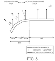
- FIG. 8 is a view for explaining a compensating area and a non-compensating area of a display panel of a display device according to an exemplary embodiment of the present disclosure.
- the luminance control unit 143 may increase the luminance of the at least one curved area 111 such that among the luminance of the at least one curved area 111, the front luminance is higher than a difference between the luminance of the plane area 112 and an identification luminance and is lower than the luminance of the plane area 112.
- the luminance control unit 143 may increase the luminance of the at least one curved area 111 so as to establish the relationship of "luminance of plane area 112 > front luminance among luminance of curved area 111 > luminance of plane area 112 - identification luminance".
- the identification luminance means a luminance difference which may be visually distinguished from a reference luminance by a viewer.
- the identification luminance tends to gradually increase as the reference luminance is increased.
- the luminance is not visually distinguished up to 347.7 cd/m 2 with respect to 350 cd/m 2 so that the identification luminance is 2.3 cd/m 2 .
- the luminance is not visually distinguished up to 994 cd/m 2 with respect to 1000 cd/m 2 so that the identification luminance is 6 cd/m 2 .
- the front luminance of the first curved area 111a is 348 c/m 2 , a difference between the luminance of the plane area 112 and the front luminance of the first curved area 111 is within the identification luminance. Therefore, even though the luminance of the first curved area 111a is not increased, the viewer does not recognize the ununiformity of the luminance.
- the viewer does not recognize the ununiformity of the luminance. That is, even though the luminances of the second curved area 111b and the third curved area 111c are increased not to 350 cd/m2, but to 347.7 cd/m 2 to 350 cd/m 2 , the viewer does not recognize the ununiformity of the luminance.
- the first curved area 111a and the plane area 112 are non-compensating areas in which compensation of the luminance is not necessary and the second curved area 111b and the third curved area 111c correspond to the compensating areas.
- an increased amount of the front luminance of the at least one curved area 111 is set in consideration of the identification luminance so that the increased amount of the luminance of each curved area 111 may be reduced.
- the power consumption due to the luminance compensating function may be reduced and the damage of the organic light emitting diode OLED due to the increased luminance may be minimized, thereby lengthening the lifespan of the display device 100.
- the gray scale control unit 145 controls gray scales of each of the pixels Px1 and Px2 so as to allow the display panel 110 to implement images.
- the gray scale control unit 145 sets a data voltage Vdata for expressing the gray scales of the pixels Px1 and Px2 after determining a data voltage Vdata for compensating the luminance of the at least one curved area 111. Specifically, the gray scale control unit 145 divides a data voltage Vdata for compensating the luminance of the at least one curved area 111 to set a data voltage Vdata for expressing the gray scales of the pixels Px1 and Px2.
- a difference of data voltages Vdata for expressing differences in individual gray scales may be constant, but may be gradually increased in consideration of visual property of the people.
- the gray scale control unit 145 outputs the image data RGB to the data driver 120 so as to reflect the data voltage Vdata determined as described above so that the image is implemented on the display panel 110.
- the luminance of the at least one curved area 111 is increased based on the viewing angle so that a constant luminance may be recognized from the front.
- the luminance uniformity of the display panel 110 is increased so that the deterioration of the image quality due to the curved area 111 may be minimized.
- FIGS. 9A and 9B are views for explaining luminance control and gray scale control of a display panel of a display device according to another exemplary embodiment of the present disclosure.
- FIGS. 9A and 9B A repeated description with the exemplary embodiment of the present disclosure will be omitted.
- an image signal VS curved corresponding to the at least one curved area 211 is controlled to increase the luminance of the at least one curved area 211.
- the luminance of a curved area 211 is increased such that a front luminance in a front direction among components of the luminance of a curved area 211 is equal to or higher than the luminance of the plane area 212.
- a first curved area 211a outputs an image while maintaining the first viewing angle ⁇ 1 with respect to the front
- a second curved area 211b outputs an image while maintaining the second viewing angle ⁇ 2 with respect to the front
- a third curved area 211c outputs an image while maintaining the third viewing angle ⁇ 3 with respect to the front. Therefore, when it is assumed that the entire areas of the display panel 210 have the same luminance, the front luminance is gradually lowered in the order of the first curved area 211a, the second curved area 211b, and the third curved area 211c with respect to the front.
- the luminance of the third curved area 211c is increased such that the front luminance of the third curved area 211c which has the lowest front luminance is equal to or higher than the luminance of the plane area 212. Further, similarly, the luminances of the first curved area 211a and the second curved area 211b are increased by an increased amount of the luminance of the third curved area 211c.
- the luminance of the at least one curved area 211 is increased by the increased amount of the luminance of the third curved area 211c so that the front luminance of the at least one curved area 211 is equal to or higher than the luminance of the plain area 212.
- the front luminance of the second curved area 211b is lower than the front luminance of the first curved area 211a.
- a third viewing angle ⁇ 3 of the third curved area 211c is larger than the second viewing angle ⁇ 2 of the second curved area 211b, the front luminance of the third curved area 211c is lower than the front luminance of the second curved area 211b.
- the gray scale control unit 245 controls the gray scale of the at least one curved area 211 such that a front luminance in a front direction among components of the luminance of the at least one curved area 211 is equal to the luminance of the plane area 212.
- the gray scale control unit 245 decreases the front luminance by differently adjusting the gray scales of the first curved area 211a, the second curved area 211b, and the third curved area 211c so that the front luminance of the at least one curved area 211 becomes uniform.
- the front luminance of the first curved area 211a is higher than the front luminance of the second curved area 211b
- a decreased amount of luminance by the gray scale adjustment of the first curved area 211a is larger than a decreased amount of luminance by the gray scale adjustment of the second curved area 211b.
- the front luminance of the second curved area 211b is higher than the front luminance of the third curved area 211c
- a decreased amount of luminance by the gray scale adjustment of the second curved area 211b is larger than a decreased amount of luminance by the gray scale adjustment of the third curved area 211c.
- the luminance control unit 243 and the gray scale control unit 245 will be described with reference to FIG. 9B as follows.
- the first viewing angle ⁇ 1 of the first curved area 211a is 15°
- the second viewing angle ⁇ 2 of the second curved area 211b is 30°
- the third viewing angle ⁇ 3 of the third curved area 211c is 45°.
- the increased amount of luminance of the at least one curved area 211 may be set such that the front luminance of the at least one curved area 211 is equal to or higher than the luminance of the plane area 212.
- the increased amount of luminance of the at least one curved area 211 is set such that the front luminance of the at least one curved area 211 is higher than the luminance of the plane area 212, for example.
- the entire front luminance is 430 cd/m 2 . Therefore, in order to set the front luminance of the third curved area 211c to be 350 cd/m 2 which is the luminance of the plane area 212, the gray scale of the third curved area 211c is decreased such that the front luminance of the third curved area 211c is decreased by 80 cd/m 2 .
- the entire front luminance is 470 cd/m 2 . Therefore, in order to set the front luminance of the second curved area 211b to be 350 cd/m 2 which is the luminance of the plane area 212, the gray scale of the second curved area 211b is decreased so that the front luminance of the second curved area 211b is decreased by 120 cd/m 2 .
- the entire front luminance is 498 cd/m 2 . Therefore, in order to set the front luminance of the first curved area 211a to be 350 cd/m 2 which is the luminance of the plane area 212, the gray scale of the first curved area 211a is decreased so that the front luminance of the first curved area 211a is decreased by 148 cd/m 2 .
- the luminance of the at least one curved area 211 is increased and the gray scale is decreased based on the viewing angle so that a constant luminance may be recognized from the front.
- the luminance uniformity of the display panel 210 is increased so that the deterioration of the image quality due to the curved area 211 may be minimized.
- the gray scale control unit 245 may decrease the gray scale of the at least one curved area 211 such that among the luminance of the at least one curved area 212, the front luminance is higher than a difference between the luminance of the plane area 212 and an identified luminance and is lower than the luminance of the plane area 212.
- the gray scale control unit 245 may decrease the gray scale of the at least one curved area 211 so as to establish the relationship of "luminance of plane area 212 > front luminance among luminance of curved area 211 > luminance of plane area 212 - identification luminance".
- the viewer may not recognize the ununiformity of the luminance. That is, even though the front luminance of the at least one curved area 211 is increased not to 350 cd/m 2 , but to 347.7 cd/m 2 to 350 cd/m 2 , the viewer does not recognize the ununiformity of the luminance.
- a decreased amount of the gray scale of the at least one curved area 211 is set in consideration of the identification luminance so that the increased amount of the luminance of each curved area 211 may be reduced.
- the power consumption due to the luminance compensating function may be reduced and the damage of the organic light emitting diode OLED due to the increased luminance may be minimized, thereby lengthening the lifespan of the display device 100.
- FIG. 10 is a flowchart for explaining a driving method of a display device according to one exemplary embodiment of the present disclosure.
- the driving method S100 of the display device includes a position tracking step S110, an image analyzing step S120, a luminance control step S130, and a gray scale control step S140.
- a position of the viewer is determined with respect to the center of the display panel 110. That is, during the position tracking step S110, it is identified whether the viewer is located within a predetermined angle with respect to the center of the display panel 110.
- a luminance compensating function by the driving method S100 of the display device is activated.
- the luminance compensating function is activated to reduce the power consumption while the viewer does not watch the display panel 110.
- the image signal VS curved corresponding to the at least one curved area 111 is analyzed to determine whether the luminance of the at least one curved area 111 is increased.
- the image signal VS curved corresponding to the at least one curved area 111 is separated, extracted, and analyzed to calculate a predicted luminance CL curved of the curved area 111. Further, during the image analyzing step, it is determined whether the luminance of the at least one curved area 111 is increased, based on the predicted luminance CL curved of the curved area 111.
- the image signal VS including 3840 image data RGB is applied during one horizontal period 1H defined by a vertical synchronization signal Vsync.
- image signals VS curved including first image data to 100-th image data and 3741-st image data to 3840-th image data which are image signals VS curved corresponding to the at least one curved area 111 are separated and extracted.
- the image data RGB of the image signal VS curved corresponding to the at least one curved area 111 is analyzed to predict a luminance CL curved of an image to be output to the curved area 111 and determine whether the luminance of the at least one curved area 111 is increased by calculating a mean square thereof.
- a predicted luminance in the at least one curved area 111 is calculated by means of Equation 1.
- CL curved RGB curved 2 bits ⁇ 1 ⁇
- CL curved means a predicted luminance in the at least one curved area 111
- RGB curved means image data of the image signal VS corresponding to the at least one curved area 111
- bits means a bit number of image data of the image signal VS
- ⁇ means a gamma constant of the display device 100.
- a mean square of the predicted luminance CL curved in the at least one curved area 111 is calculated by means of Equation 2 to determine whether to compensate the luminance of the at least one curved area 111.
- WF curved ⁇ CL curved 2 ⁇ CL curved
- WF curved means a mean square value of the predicted luminance CL curved and may have a value between 0 to 1. This becomes an index for determining whether the luminance of the at least one curved area 111 of the display device 100 according to the exemplary embodiment of the present disclosure is increased.
- the viewer may not recognize the luminance deterioration by the curved area 111 at the low luminance but may apparently recognize the luminance deterioration by the curved area 111 at a relatively high luminance. Therefore, the luminance of the at least one curved area 111 needs to be compensated only at a relatively high luminance.
- the luminance of the at least one curved area 111 is increased and when the mean square value is equal to or lower than 0.9, the luminance of the at least one curved area 111 may not be increased.
- the luminance of the at least one curved area 111 may be gradually increased.
- a luminance boost ratio of the curved area 111 may be set to be proportional to the mean square value WF curved of the predicted luminance.
- the luminance compensating function of the display device 100 is activated based on the mean value WF curved of the square of the predicted luminance to reduce the power consumption by the luminance compensating function. Further, the damage of the organic light emitting diode OLED due to the increased luminance is minimized, thereby lengthening the lifespan of the display device 100.
- an image signal VS curved corresponding to the at least one curved area 111 is controlled to increase the luminance of the at least one curved area 111.
- the luminance of the at least one curved area 111 is increased such that a front luminance in a front direction among components of the luminance of the at least one curved area 111 is equal to the luminance of the plane area 112.
- the first curved area 111a outputs an image while maintaining the first viewing angle ⁇ 1 with respect to the front
- the second curved area 111b outputs an image while maintaining the second viewing angle ⁇ 2 with respect to the front
- the third curved area 111c outputs an image while maintaining the third viewing angle ⁇ 3 with respect to the front. Therefore, when it is assumed that the entire areas of the display panel 110 have the same luminance, the front luminance is gradually lowered in the order of the first curved area 111a, the second curved area 111b, and the third curved area 111c with respect to the front.
- the luminance of the at least one curved area 111 is increased such that the front luminance is equal to the luminance of the plane area 112. Since the second viewing angle ⁇ 2 of the second curved area 111b is larger than the first viewing angle ⁇ 1 of the first curved area 111a, the increased luminance of the second curved area 111b is higher than the increased luminance of the first curved area 111a. Further, since the third viewing angle ⁇ 3 of the third curved area 111c is larger than the second viewing angle ⁇ 2 of the second curved area 111b, the increased luminance of the third curved area 111c is higher than the increased luminance of the second curved area 111b.
- the luminance control step S130 will be described with reference to FIG. 7B as follows.
- the first viewing angle ⁇ 1 of the first curved area 111a is 15°
- the second viewing angle ⁇ 2 of the second curved area 111b is 30°
- the third viewing angle ⁇ 3 of the third curved area 111c is 45°.
- the front luminance and the luminance boost ratio of the curved area 111 in accordance with the viewing angle of the curved area 111 are represented in Table 1.
- Table 1 Viewing angle [°] 0 15 30 45 Front luminance [cd/m 2 ] 350 348 320 280 Boost Ratio 1 1.01 1.1 1.25 Vdata[v] 3.2 3.2 3.5 3.9
- a front luminance of the first curved area 111a is 348 cd/m 2 . Therefore, in order to set the front luminance of the first curved area 111a to be 350 cd/m 2 which is the luminance of the plane area 112, the luminance of the first curved area 111a needs to be increased by 1.01 times.
- a front luminance of the second curved area 111b is 320 cd/m 2 . Therefore, in order to set the front luminance of the second curved area 111b to be 350 cd/m 2 which is the luminance of the plane area 112, the luminance of the second curved area 111b needs to be increased by 1.1 times.
- a front luminance of the third curved area 111c is 280 cd/m 2 . Therefore, in order to set the front luminance of the third curved area 111c to be 350 cd/m 2 which is the luminance of the plane area 112, the luminance of the third curved area 111c needs to be increased by 1.25 times.
- the luminance of the at least one curved area 111 is increased based on the viewing angle so that a constant luminance may be recognized from the front.
- the luminance uniformity of the display panel 110 is increased so that the deterioration of the image quality due to the curved area 111 may be minimized.
- the luminance of the at least one curved area 111 may be increased such that among the luminance of the at least one curved area 111, the front luminance is higher than a difference between the luminance of the plane area 112 and an identified luminance and is lower than the luminance of the plane area 112.
- the luminance of the at least one curved area 111 may be increased so as to establish the relationship of "luminance of plane area 112 > front luminance among luminance of curved area 111 > luminance of plane area 112 - identification luminance".
- the identification luminance means a luminance difference which may be visibly distinguished from a reference luminance by a viewer.
- the identification luminance tends to gradually increase as the reference luminance is increased.
- the luminance is not visually distinguished up to 347.7 cd/m 2 with respect to 350 cd/m 2 so that the identification luminance is 2.3 cd/m 2 .
- the luminance is not visually distinguished up to 994 cd/m 2 with respect to 1000 cd/m 2 so that the identification luminance is 6 cd/m 2 .
- the front luminance of the first curved area 111a is 348 c/m 2 , a difference between the luminance of the plane area 112 and the front luminance of the first curved area 111 is within the identification luminance. Therefore, even though the luminance of the first curved area 111a is not increased, the viewer does not recognize the ununiformity of the luminance.
- the front luminances of the second curved area 111b and the third curved area 111c are increased to be higher than a difference between the luminance of the plane area 112 and the identification luminance and lower than the luminance of the plane area 112, the viewer does not recognize the ununiformity of the luminance. That is, even though the luminances of the second curved area 111b and the third curved area 111c are increased not to 350 cd/m2, but to 347.7 cd/m 2 to 350 cd/m 2 , the viewer does not recognize the ununiformity of the luminance.
- the first curved area 111a and the plane area 112 are non-compensating areas in which compensation of the luminance is not necessary and the second curved area 111b and the third curved area 111c correspond to the compensating areas.
- an increased amount of the front luminance of the at least one curved area 111 is set in consideration of the identification luminance so that the increased amount of the luminance of each curved area 111 may be reduced.
- the power consumption due to the luminance compensating function may be reduced and the damage of the organic light emitting diode OLED due to the increased luminance may be minimized, thereby lengthening the lifespan of the display device 100.
- gray scales of each of the pixels Px1 and Px2 are controlled so as to allow the display panel 110 to implement images.
- a data voltage Vdata for expressing the gray scales of the pixels Px1 and Px2 is set after determining a data voltage Vdata for compensating the luminance of the at least one curved area 111.
- a data voltage Vdata for expressing the gray scales of the pixels Px1 and Px2 is set by dividing a data voltage Vdata for compensating the luminance of the at least one curved area 111.
- the luminance of the at least one curved area 111 is increased based on the viewing angle so that a constant luminance may be recognized from the front.
- the luminance uniformity of the display panel 110 is increased so that the deterioration of the image quality due to the curved area 111 may be minimized.
- an image signal VS curved corresponding to a curved area 211 is controlled to increase the luminance of the at least one curved area 211.
- the luminance of the at least one curved area 211 is increased such that a front luminance in a front direction among components of the luminance of the at least one curved area 211 is equal to or higher than the luminance of the plane area 212.
- a first curved area 211a outputs an image while maintaining the first viewing angle ⁇ 1 with respect to the front
- a second curved area 211b outputs an image while maintaining the second viewing angle ⁇ 2 with respect to the front
- a third curved area 211c outputs an image while maintaining the third viewing angle ⁇ 3 with respect to the front. Therefore, when it is assumed that the entire areas of the display panel 210 have the same luminance, the front luminance is gradually lowered in the order of the first curved area 211a, the second curved area 211b, and the third curved area 211c with respect to the front.
- the luminance of the third curved area 211c is increased such that the front luminance of the third curved area 211c which has the lowest front luminance is equal to or higher than the luminance of the plane area 212. Further, the luminances of the first curved area 211a and the second curved area 211b are increased by an increased amount of the luminance of the third curved area 211c.
- the luminance of the at least one curved area 211 is increased by the increased amount of the luminance of the third curved area 211c so that the front luminance of the at least one curved area 211 is equal to or higher than the luminance of the plain area 212.
- a second viewing angle ⁇ 2 of the second curved area 211b is larger than a first viewing angle ⁇ 1 of the first curved area 211a
- the front luminance of the second curved area 211b is lower than the front luminance of the first curved area 211a.
- a third viewing angle ⁇ 3 of the third curved area 211c is larger than the second viewing angle ⁇ 2 of the second curved area 211b
- the front luminance of the third curved area 211c is lower than the front luminance of the second curved area 211b.
- the gray scale of the at least one curved area 211 is controlled such that a front luminance in a front direction among components of the luminance of the at least one curved area 211 is equal to the luminance of the plane area 212.
- the front luminance is decreased by differently adjusting the gray scales of the first curved area 211a, the second curved area 211b, and the third curved area 211c so that the front luminance of the at least one curved area 211 becomes uniform.
- an amount of decreased luminance by the gray scale adjustment of the first curved area 211a is larger than an amount of decreased luminance by the gray scale adjustment of the second curved area 211b.
- an amount of decreased luminance by the gray scale adjustment of the second curved area 211b is larger than an amount of decreased luminance by the gray scale adjustment of the third curved area 211c.
- the luminance control unit 243 and the gray scale control unit 245 will be described with reference to FIG. 9B as follows.
- the first viewing angle ⁇ 1 of the first curved area 211a is 15°
- the second viewing angle ⁇ 2 of the second curved area 211b is 30°
- the third viewing angle ⁇ 3 of the third curved area 211c is 45°.
- the amount of increased luminance of the at least one curved area 211 may be set such that the front luminance of the at least one curved area 211 is equal to or higher than the luminance of the plane area 212.
- the amount of increased luminance of the at least one curved area 211 is set such that the front luminance of the at least one curved area 211 is higher than the luminance of the plane area 212, for example.
- the entire front luminance is 430 cd/m 2 . Therefore, in order to set the front luminance of the third curved area 211c to be 350 cd/m 2 which is the luminance of the plane area 212, the gray scale of the third curved area 211c is decreased such that the front luminance is decreased by 80 cd/m 2 .
- the entire front luminance is 470 cd/m 2 . Therefore, in order to set the front luminance of the second curved area 211b to be 350 cd/m 2 which is the luminance of the plane area 212, the gray scale of the second curved area 211b is decreased so that the front luminance is decreased by 120 cd/m 2 .
- the entire front luminance is 498 cd/m 2 . Therefore, in order to set the front luminance of the first curved area 211a to be 350 cd/m 2 which is the luminance of the plane area 212, the gray scale of the first curved area 211a is decreased so that the front luminance is decreased by 148 cd/m 2 .
- the luminance of the at least one curved area 211 is increased and the gray scale is decreased based on the viewing angle so that a constant luminance may be recognized from the front.
- the luminance uniformity of the display panel 210 is increased so that the deterioration of the image quality due to the curved area 211 may be minimized.
- the gray scale of the at least one curved area 211 is decreased such that among the luminance of the at least one curved area 212, the front luminance is higher than a difference between the luminance of the plane area 212 and an identified luminance and is lower than the luminance of the plane area 212.
- the gray scale control unit 245 may decrease the gray scale of the at least one curved area 211 so as to establish the relationship of "luminance of plane area 212 > front luminance among luminance of curved area 211 > luminance of plane area 212 - identification luminance".
- the front luminance of the at least one curved area 211 is increased to be higher than a difference between the luminance of the plane area 212 and the identification luminance and to be lower than the luminance of the plane area 212, the viewer may not recognize the ununiformity of the luminance. That is, the luminance of the at least one curved area 211 is increased not to 350 cd/m 2 , but to 347.7 cd/m 2 to 350 cd/m 2 , the viewer does not recognize the ununiformity of the luminance.
- a decreased amount of the gray scale of the at least one curved area 211 is set in consideration of the identification luminance so that the increased amount of the luminance of each curved area 211 may be reduced.
- a display device includes: a display panel which includes a plane area and at least one curved area disposed at the outside of the plane area; a timing controller which is applied with an image signal to generate image data; and a data driver which is applied with the image data to output a data voltage to a plurality of pixels disposed in the plane area and in the at least one curved areaa plurality of pixels disposed in the at least one curved area in which the timing controller includes an image analyzing unit which analyzes the corresponding to the at least one curved areaimage signal corresponding to the at least one curved area and a luminance control unit which controls the corresponding to the at least one curved areaimage signal corresponding to the at least one curved area to increase luminance of the at least one curved areaa luminance of the at least one curved area.
- the display device may further include: a position tracking unit which tracks a position of a viewer to generate a location signal including a location information of the viewer and the image analyzing unit may determine whether to increase the luminance of the at least one curved area, based on the location signal.
- the image analyzing unit may analyze an corresponding to the at least one curved areaimage signal corresponding to the at least one curved area to calculate a predicted luminance of the at least one curved area and determine whether to increase the luminance of the at least one curved area, based on the predicted luminance of the at least one curved area.
- the data driver may increase a data voltage output to the plurality of pixels disposed in the at least one curved area, based on the image data corresponding to the at least one curved area, and the plurality of pixels disposed in the at least one curved area may include at least one organic light emitting diode, and a driving current of the at least one organic light emitting diode may be increased by the increased data voltage.
- the luminance control unit may increase the luminance of the at least one curved area such that a front luminance among the luminance of the at least one curved area is equal to the luminance of the plane area.
- the luminance control unit may increase the luminance of the at least one curved area such that a front luminance among the luminance of the at least one curved area is higher than a difference between the luminance of the plane area and an identification luminance and is lower than the luminance of the plane area.
- the timing controller may further include a gray scale control unit which controls a gray scale of the at least one curved area
- the luminance control unit may increases the luminance of the at least one curved area such that a front luminance among the luminance of the at least one curved area is equal to or higher than the luminance of the plane area
- the gray scale control unit may decrease the gray scale of the at least one curved area.
- the gray scale control unit may decrease the gray scale of the at least one curved area such that a front luminance among the luminance of the at least one curved area is equal to the luminance of the plane area.
- the gray scale control unit may decrease a gray scale of the at least one curved area such that a front luminance among the luminance of the at least one curved area is higher than a difference between the luminance of the plane area and an identification luminance and is lower than the luminance of the plane area.
- a driving method of a display device includes an image analyzing step of analyzing an corresponding to the at least one curved areaimage signal corresponding to the at least one curved area and a luminance control step of increasing luminance of the at least one curved areaa luminance of the at least one curved area.
- the driving method may further include a gray scale control step of increasing the luminance of the at least one curved area such that a front luminance among the luminance of the at least one curved area is equal to or higher than the luminance of the plane area and decreasing a gray scale of the at least one curved area.
- the gray scale of the at least one curved area may be decreased such that a front luminance among the luminance of the at least one curved area is equal to the luminance of the plane area.
- a gray scale of the at least one curved area may be decreased such that a front luminance among the luminance of the at least one curved area is higher than a difference between the luminance of the plane area and an identification luminance and is lower than the luminance of the plane area.
Abstract
Description
- This application claims the priority of Korean Patent Application No.
10-2017-0083418 filed on June 30, 2017 - The present disclosure relates to a display device and a driving method of the same, and more particularly, to a display device and a driving method of the same which increase a luminance of a curve area according to a viewing angle to uniformly control the luminance.
- As the information society is developed, demands for display devices for displaying images are increased in various forms. Recently, various display devices such as a liquid crystal display device, a plasma display panel, and an organic light emitting display device are utilized.
- The display devices include a display panel in which data lines and gate lines are disposed and pixels are disposed at the intersections of the data lines and the gate lines. Further, the display devices include a data driver which supplies a data voltage to the data lines, a gate driver which supplies a gate voltage to the gate lines, and a timing controller which controls the data driver and the gate driver.
- Specifically, recently, a flexible organic light emitting display device (flexible OLED) which may implement an image quality at it is using a flexible substrate even though a display panel is bent has been developed.
- A display panel of the flexible organic light emitting display device is divided into a flat plain area and a curved area which is bent at the outside of the plain area and an entire image is output through the plain area and the curved area. Here, a viewing angle of the plane area is 0° with respect to a front, but the curved area has a predetermined viewing angle with respect to a front.
- In the related art, a luminance of a display panel which outputs the entire image is set to be constant based on a luminance of the plane area, regardless of the plane area and the curved area.
- In this case, as seen from the front which is a viewing position, a luminance of the plane area is appropriately set to normally output an image. However, the luminance of the at least one curved area is recognized to be lower than the luminance of the plane area with respect to the front, due to a viewing angle of the curved area.
- Accordingly, the flexible organic light emitting display device of the related art does not recognize uniform luminance through the entire display panel, so that image quality may be deteriorated due to luminance unevenness of the display panel.
- In an aspect, a display device is provided as defined in
claim 1. - In another aspect, a driving method of a display device is provided as defined in claim 10.
- An object to be achieved by the present disclosure is to provide a display device and a driving method of the same which control the luminance to be uniform by increasing the luminance of the at least one curved area in accordance with the viewing angle.
- Another object to be achieved by the present disclosure is to provide a display device and a driving method of the same which reduce the power consumption by activating a luminance compensating function based on an image signal.
- Objects of the present disclosure are not limited to the above-mentioned objects, and other objects, which are not mentioned above, can be clearly understood by those skilled in the art from the following descriptions.
- According to an example of the present disclosure, a display device includes: a display panel which includes a plane area and at least one curved area disposed at the outside of the plane area; a timing controller which is applied with an image signal to generate image data; and a data driver which is applied with the image data to output a data voltage to a plurality of pixels disposed in the plane area and in the at least one curved areaa plurality of pixels disposed in the at least one curved area in which the timing controller includes an image analyzing unit which analyzes the corresponding to the at least one curved areaimage signal corresponding to the at least one curved area and a luminance control unit which controls the corresponding to the at least one curved areaimage signal corresponding to the at least one curved area to increase luminance of the at least one curved areaa luminance of the at least one curved area.
- According to another example of the present disclosure, a driving method of a display device includes an image analyzing step of analyzing an corresponding to the at least one curved areaimage signal corresponding to the at least one curved area and a luminance control step of increasing luminance of the at least one curved areaa luminance of the at least one curved area.
- Other detailed matters of the embodiments are included in the detailed description and the drawings.
- According to the present disclosure, the luminance of the at least one curved area is increased based on the viewing angle to increase the luminance uniformity of the display panel, thereby minimizing the deterioration of the image quality due to the curved area.
- Further, according to the present disclosure, only when it is determined that a viewer watches the display device, the luminance compensating function is activated based on an average of a square of predicted luminance to reduce the power consumption due to the luminance compensating function and minimize a damage of an organic light emitting diode due to the increased luminance, thereby lengthening the lifespan of the display device.
- The effects according to the present disclosure are not limited to the contents exemplified above, and more various effects are included in the present specification.
- The above and other examples, features and other advantages of the present disclosure will be more clearly understood from the following detailed description taken in conjunction with the accompanying drawings, in which:
-
FIG. 1 is a schematic block diagram for explaining a display device according to an exemplary embodiment of the present disclosure; -
FIG. 2 is a view illustrating a display panel of a display device according to an exemplary embodiment of the present disclosure; -
FIG. 3 is a circuit diagram illustrating a pixel disposed on a display panel of a display device according to an exemplary embodiment of the present disclosure; -
FIGS. 4A and4B are schematic views for explaining a display panel of a display device according to an exemplary embodiment of the present disclosure and a viewing position; -
FIG. 5 is a schematic block diagram for explaining a timing controller of a display device according to an exemplary embodiment of the present disclosure; -
FIG. 6 is a timing chart for explaining an internal signal of a timing controller of a display device according to an exemplary embodiment of the present disclosure; -
FIGS. 7A and7B are views for explaining luminance control of a display panel of a display device according to an exemplary embodiment of the present disclosure; -
FIG. 8 is a view for explaining a compensating area and a non-compensating area of a display panel of a display device according to an exemplary embodiment of the present disclosure; -
FIGS. 9A and9B are views for explaining luminance control and gray scale control of a display panel of a display device according to another exemplary embodiment of the present disclosure; and -
FIG. 10 is a flowchart for explaining a driving method of a display device according to one exemplary embodiment of the present disclosure. - Advantages and characteristics of the present disclosure and a method of achieving the advantages and characteristics will be clear by referring to exemplary embodiments described below in detail together with the accompanying drawings. However, the present disclosure is not limited to the exemplary embodiment disclosed herein but will be implemented in various forms. The exemplary embodiments are provided by way of example only so that a person of ordinary skill in the art can fully understand the present disclosure and the scope of the present disclosure. Therefore, the present disclosure will be defined only by the scope of the appended claims.
- Further, in the following description, a detailed explanation of known related technologies may be omitted to avoid unnecessarily obscuring the subject matter of the present disclosure. The terms such as "including," "having," and "consist of" used herein are generally intended to allow other components to be added unless the terms are used with the term "only". Any references to singular may include plural unless expressly stated otherwise.
- Components are interpreted to include an ordinary error range even if not expressly stated.
- Although the terms "first", "second", and the like are used for describing various components, these components are not confined by these terms. These terms are merely used for distinguishing one component from the other components. Therefore, a first component to be mentioned below may be a second component in a technical concept of the present disclosure.
- Like reference numerals generally denote like elements throughout the specification.
- The features of various embodiments of the present disclosure can be partially or entirely bonded to or combined with each other and can be interlocked and operated in technically various ways understood by those skilled in the art, and the embodiments can be carried out independently of or in association with each other.
- Hereinafter, various exemplary embodiments of the present disclosure will be described in detail with reference to accompanying drawings.
-
FIG. 1 is a schematic block diagram for explaining a display device according to an exemplary embodiment of the present disclosure. - Referring to
FIG. 1 , adisplay device 100 includes adisplay panel 110, adata driver 120, agate driver 130, atiming controller 140, and aposition tracking unit 150. - The
display panel 110 is configured such that a plurality of gate lines GL1 to GLm and a plurality of data lines DL1 to DLn intersect each other to be formed in a matrix on a substrate which uses glass or plastic. A plurality of pixels Px1 and Px2 is defined at the intersections of the plurality of gate lines GL1 to GLm and the plurality of data lines DL1 to DLn. - Here, the substrate may be a flexible substrate. That is, a substrate of a
display device 100 according to an exemplary embodiment of the present disclosure has a predetermined elasticity to be bent by an external force. To this end, the substrate may be formed of polymer plastic having a bending property such as polyimide (PI). - Each of the pixels Px1 and Px2 of the
display panel 110 includes at least one thin film transistor. A gate electrode of the thin film transistor is connected to the gate line GL1 to GLm and a source electrode is connected to the data line DL1 to DLn. - When the
display device 100 according to an exemplary embodiment of the present disclosure is a liquid crystal display device, a drain electrode is connected to a pixel electrode facing a common electrode to control a voltage which is applied to liquid crystal. By doing this, movement of the liquid crystal is controlled to implement a gray scale of the liquid crystal display device. - Further, when the
display device 100 according to the exemplary embodiment of the present disclosure is an organic light emitting display device, current is applied to an organic light emitting diode (OLED inFIG. 3 ) equipped in the plurality of pixels Px1 and Px2 and discharged electrons and holes are coupled to generate excitons. The excitons emit light to implement the gray scale of the organic light emitting display device. Details thereof will be described below with reference toFIG. 3 . - As described above, the
display device 100 according to the exemplary embodiment of the present disclosure is not limited to the liquid crystal display and the organic light emitting display device, but may be various types of display devices. -
FIG. 2 is a view illustrating a display panel of a display device according to an exemplary embodiment of the present disclosure. - The
display panel 110 may include aplane area 112 and acurved area 111. Theplane area 112 is disposed at a center portion of thedisplay panel 110 and outputs an image to the front which is a viewing position. Thecurved area 111 is disposed to be divided into at least onecurved area 111 at an outside of theplane area 112. Thecurved area 111 does not output the image to the front which is a viewing position, but outputs an image while maintaining a predetermined viewing angle with respect to the front. InFIG. 1 , theplane area 112 and thecurved area 111 are divided to have a predetermined area, but this is merely an example. Theplane area 112 and thecurved area 111 may vary in accordance with a bending property of thedisplay device 100. - More specifically, referring to
FIG. 2 , thecurved area 111 of thedisplay panel 110 may be divided into a firstcurved area 111a, a secondcurved area 111b, and a thirdcurved area 111c having different curvatures. Here, the curvature of the secondcurved area 111b is larger than the curvature of the firstcurved area 111a and the curvature of the thirdcurved area 111c is larger than the curvature of the secondcurved area 111b. That is, with respect to theplane area 112, a bending angle θ2 of the secondcurved area 111b is larger than a bending angle θ1 of the firstcurved area 111a and a bending angle θ3 of the thirdcurved area 111c is larger than the bending angle θ2 of the secondcurved area 111b. - Therefore, with respect to the front which is a viewing position, a second viewing angle θ2 of an image output from the second
curved area 111b is larger than a first viewing angle θ1 of an image output from the firstcurved area 111a and a third viewing angle θ3 of an image output from the thirdcurved area 111c is larger than the second viewing angle θ2 of an image output from the secondcurved area 111b. - Even though in
FIG. 2 , it is illustrated that the bending angle is increased in the at least onecurved area 111 disposed at an outer edge of thedisplay panel 110, it is not limited thereto and the bending angle may vary depending on an external force which is applied to thedisplay panel 110. - In the
plane area 112 and thecurved area 111, a plurality of pixels Px1 and Px2 may be disposed. The plurality of pixels Px2 disposed in theplane area 112 and the plurality of pixels Px1 disposed in the at least onecurved area 111 may be distinguished. - Each of the pixels Px1 and Px2 may include a plurality of sub pixels and each sub pixel may implement light of a specific color. For example, the plurality of sub pixels may be configured by a red sub pixel which implements red, a green sub pixel which implements green, and a blue sub pixel which implements blue, but is not limited thereto.
-
FIG. 3 is a circuit diagram illustrating a pixel disposed on a display panel of a display device according to an exemplary embodiment of the present disclosure. - The driving of each of the pixels Px1 and Px2 will be described with reference to
FIG. 3 as follows. First, a switching transistor ST is turned on by a gate voltage which is supplied to the gate lines GL1 to GLm of each of the pixels Px1 and Px2. Further, a data voltage Vdata is supplied from the data lines DL1 to DLn by the turned-on switching transistor ST and a driving current i is controlled by a driving transistor DT which is applied with the data voltage. Finally, the organic light emitting diode OLED emits light corresponding to the controlled driving current i to display images. -
FIGS. 4A and4B are schematic views for explaining a display panel of a display device according to an exemplary embodiment of the present disclosure and a viewing position. - The
position tracking unit 150 tracks a position of a viewer to generate a location signal LS. - That is, the
position tracking unit 150 generates a location signal LS including a location information of the viewer with respect to the center of thedisplay panel 110. Here, the location information indicates that the viewer is located within a predetermined angle with respect to the center of thedisplay panel 110. - The
position tracking unit 150 may be configured by a camera which may recognize the position of the viewer, but is not limited thereto and all devices which are capable of figuring out the location of the viewer may correspond to theposition tracking unit 150. - Specifically, referring to
FIG. 4A , when an angle at which the viewer is located is 10° or less with respect to a long axis of thedisplay panel 110, theposition tracking unit 150 determines that the viewer is watching thedisplay device 100. - Further, referring to
FIG. 4B , when an angle at which the viewer is located is 40° or less with respect to a short axis of thedisplay panel 110, theposition tracking unit 150 determines that the viewer is watching thedisplay device 100. - Therefore, the
position tracking unit 150 generates the location signal LS by combining them. That is, only when the angle at which the viewer is located is 10° or less with respect to the long axis of thedisplay panel 110 and the angle at which the viewer is located is 40° or less with respect to the short axis of thedisplay panel 110, theposition tracking unit 150 outputs an on-level location signal LS to activate a luminance compensating function of thedisplay device 100 according to an exemplary embodiment of the present disclosure. - As described above, there is an advantage in that only when it is determined that the viewer watches the
display device 100, the luminance compensating function is activated to reduce the power consumption while the viewer does not watch thedisplay panel 110. - The
timing controller 140 supplies various control signals DCS and GCS and image data RGB to thedata driver 120 and thegate driver 130 to control thedata driver 120 and thegate driver 130. - The
timing controller 140 starts scanning in accordance with a timing implemented by each frame, based on the timing signal TS received from an external host system. Thetiming controller 140 converts an image signal VS received from the external host system in accordance with an image data RGB format which is processible in thedata driver 120. Further, thetiming controller 140 adjusts the luminance of the at least onecurved area 111 by analyzing the image signal VScurved corresponding to the at least onecurved area 111 to make the luminance in the front of thedisplay panel 110 uniform. Details thereof will be described below with reference toFIG. 5 . - More specifically, the
timing controller 140 receives various timing signals TS including a vertical synchronization signal Vsync, a horizontal synchronization signal Hsync, a data enable signal DE, and a data clock signal DCLK together with an image signal VS from the external host system. - In order to control the
data driver 120 and thegate driver 130, thetiming controller 140 receives the timing signal TS such as the vertical synchronization signal Vsync, the horizontal synchronization signal Hsync, the data enable signal DE, and the data clock signal DCLK and generates various control signals DCS and GCS. Thetiming controller 140 outputs the various control signals DCS and GCS to thedata driver 120 and thegate driver 130. - For example, in order to control the
gate driver 130, thetiming controller 140 outputs various gate control signals GCS including a gate start pulse GSP, a gate shift clock GSC, and a gate output enable signal GOE. - Here, the gate start pulse controls an operation start timing of one or more gate circuits which configure the
gate driver 130. The gate shift clock is a clock signal which is commonly input to one or more gate circuits and controls a shift timing of the scan signal (gate pulse). The gate output enable signal designates timing information of one or more gate circuits. - Further, in order to control the
data driver 120, thetiming controller 140 outputs various data control signals DCS including a source start pulse SSP, a source sampling clock SSC, and a source output enable signal SOE. - Here, the source start pulse controls a data sampling start timing of one or more data circuits which configure the
data driver 120. The source sampling clock is a clock signal which controls a sampling timing of data in each data circuit. The source output enable signal controls an output timing of thedata driver 120. - The
timing controller 140 may be disposed on a control printed circuit board which is connected to a source printed circuit board to which thedata driver 120 is bonded through a connecting medium such as a flexible flat cable (FFC) or a flexible printed circuit (FPC). - In the control printed circuit board, a power controller which supplies various voltages or currents to the
display panel 110, thedata driver 120, and thegate driver 130 or controls various voltages or currents to be supplied may be further disposed. The power controller may also be referred to as a power management integrated circuit (PMIC). - The source printed circuit board and the control printed circuit board described above may be configured by one printed circuit board.
- The
gate driver 130 sequentially supplies a gate voltage which is an on-voltage or an off-voltage to the gate lines GL1 to GLm in accordance with the control of thetiming controller 140. - According to a driving method, the
gate driver 130 may be located only at one side of thedisplay panel 110 or located at both sides if necessary. - The
gate driver 130 may be connected to a bonding pad of thedisplay panel 110 by means of a tape automated bonding (TAB) method or a chip on glass (COG) method. Thegate driver 130 may be implemented to be a gate in panel (GIP) type to be directly disposed in thedisplay panel 110 or may be integrated to be disposed in thedisplay panel 110, if necessary. - The
gate driver 130 may include a shift register or a level shifter. - The
data driver 120 converts image data RGB received from thetiming controller 140 into an analog data voltage Vdata to output the analog data voltage to the data lines DL1 to DLn. - The
data driver 120 is connected to the bonding pad of thedisplay panel 110 by a tape automated bonding method or a chip on glass method or may be directly disposed on thedisplay panel 110. If necessary, thedata driver 120 may be integrated to be disposed in thedisplay panel 110. - Further, the
data driver 120 may be implemented by a chip on film (COF) method. In this case, one end of thedata driver 120 may be bonded to at least one source printed circuit board and the other end may be bonded to thedisplay panel 110. - The
data driver 120 may include a logic unit including various circuits such as a level shifter or a latch unit, a digital analog converter DAC, and an output buffer. -
FIG. 5 is a schematic block diagram for explaining a timing controller of a display device according to an exemplary embodiment of the present disclosure; - Referring to
FIG. 5 , thetiming controller 140 according to the exemplary embodiment of the present disclosure includes animage analyzing unit 141, aluminance control unit 143, and a grayscale control unit 145. -
FIG. 6 is a timing chart for explaining an internal signal of a timing controller of a display device according to an exemplary embodiment of the present disclosure. - The
image analyzing unit 141 determines whether the luminance of the at least onecurved area 111 is increased, based on the location signal LS. - That is, when the on-level location signal LS is applied, the
image analyzing unit 141 increases the luminance of the at least onecurved area 111. In contrast, when the off-level location signal LS is applied, theimage analyzing unit 141 does not increase the luminance of the at least onecurved area 111. - As described above, there is an advantage in that only when it is determined that the viewer watches the
display device 100, the luminance compensating function is activated to reduce the power consumption while the viewer does not watch thedisplay panel 110. - The
image analyzing unit 141 analyzes the image signal VScurved corresponding to the at least onecurved area 111 to determine whether the luminance of the at least onecurved area 111 is increased. - In other words, the
image analyzing unit 141 separates, extracts, and analyzes the image signal VScurved corresponding to the at least onecurved area 111 to calculate a predicted luminance CLcurved of thecurved area 111. Further, theimage analyzing unit 141 determines whether the luminance of the at least onecurved area 111 is increased, based on the predicted luminance CLcurved of thecurved area 111. - Specifically, an operation of the
image analyzing unit 141 will be described with reference toFIG. 6 as follows. For the convenience of description, it is assumed that the image signal VS including 3840 image data RGB is applied during onehorizontal period 1H defined by a vertical synchronization signal Vsync. - The
image analyzing unit 141 generates a count signal (pixel count: PC) indicating an order of image data RGB included in the image signal VS during onehorizontal period 1H. As illustrated inFIG. 6 , the image signal VS includes 3840 image data RGB, so that the count signal PC periodically repeats values of 1 to 3840. - The
image analyzing unit 141 separates and extracts an image signal VScurved corresponding to the at least onecurved area 111, in accordance with a predetermined area signal AS. - Here, the area signal AS is in an on-level during a section when an image signal VScurved corresponding to the at least one
curved area 111 is output and is in an off-level during a section when an image signal VS corresponding to theplane area 112 is output. - Specifically, the area signal AS is in an on-level during sections corresponding to first image data to 100-th image data and sections corresponding to 3741-st image data to 3840-th image data and is in an off-level during remaining sections corresponding to 101-st image data to 3740-th image data.
- By doing this, the
image analyzing unit 141 separates and extracts an area signal VScurved of a section when the image signal AS is in an on-level. That is, theimage analyzing unit 141 separates and extracts image signals VScurved including first to 100-th image data and 3741-st image data to 3840-th image data. - Next, the
image analyzing unit 141 analyzes the image data RGB of the image signal VScurved corresponding to the at least onecurved area 111 to predict a luminance CLcurved of an image to be output to thecurved area 111 and determine whether the luminance of the at least onecurved area 111 is increased by calculating a mean square thereof. - Specifically, the
image analyzing unit 141 calculates a predicted luminance in the at least onecurved area 111 by means ofEquation 1.
- Here, CLcurved means a predicted luminance in the at least one
curved area 111, RGBcurved means image data of the image signal VS corresponding to the at least onecurved area 111, bits means a bit number of image data of the image signal VS, and γ means a gamma constant of thedisplay device 100. - The
image analyzing unit 141 calculates a mean square of the predicted luminance CLcurved in the at least onecurved area 111 by means ofEquation 2 to determine whether to compensate the luminance of the at least onecurved area 111.
- Here, WFcurved means a mean square value of the predicted luminance CLcurved and may have a value between 0 to 1. This becomes an index for determining whether the luminance of the at least one
curved area 111 of thedisplay device 100 according to the exemplary embodiment of the present disclosure is increased. - With regard to this, the viewer may not recognize luminance deterioration by the
curved area 111 at the low luminance but may apparently recognize the luminance deterioration by thecurved area 111 at a relatively high luminance. Therefore, there is a necessity to compensate the luminance of the at least onecurved area 111 only at a relatively high luminance. - Therefore, only when a mean square value WFcurved of the predicted luminance which means a relative intensity of the luminance is equal to or higher than a predetermined value, the luminance of the at least one
curved area 111 is increased. - For example, only when a mean square value WFcurved of the predicted luminance is equal to or higher than 0.9, the luminance of the at least one
curved area 111 is increased and when the mean square value is equal to or lower than 0.9, the luminance of the at least onecurved area 111 may not be increased. - Alternatively, as the mean square value WFcurved of the predicted luminance is increased, the luminance of the at least one
curved area 111 may be gradually increased. For example, when the mean square value WFcurved of the predicted luminance is equal to or higher than 0.75 and equal to or lower than 1, a luminance boost ratio of thecurved area 111 may be set to be proportional to the mean square value WFcurved of the predicted luminance. - As described above, the luminance compensating function of the
display device 100 according to the exemplary embodiment of the present disclosure is activated based on the mean value WFcurved of the square of the predicted luminance to reduce the power consumption due to the luminance compensating function. Further, the damage of the organic light emitting diode OLED due to the increased luminance is minimized, thereby lengthening the lifespan of thedisplay device 100. -
FIGS. 7A and7B are views for explaining luminance control of a display panel of a display device according to an exemplary embodiment of the present disclosure. - The
luminance control unit 143 controls an image signal VScurved corresponding to the at least onecurved area 111 to increase the luminance of the at least onecurved area 111. - That is, the
luminance control unit 143 increases the luminance of the at least onecurved area 111 such that a front luminance in a front direction among components of the luminance of the at least onecurved area 111 is equal to the luminance of theplane area 112. - Referring to
FIG. 7A , the firstcurved area 111a outputs an image while maintaining the first viewing angle θ1 with respect to the front, the secondcurved area 111b outputs an image while maintaining the second viewing angle θ2 with respect to the front, and the thirdcurved area 111c outputs an image while maintaining the third viewing angle θ3 with respect to the front. Therefore, when it is assumed that the entire areas of thedisplay panel 110 have the same luminance, the front luminance is gradually lowered in the order of the firstcurved area 111a, the secondcurved area 111b, and the thirdcurved area 111c with respect to the front. - In order to solve the luminance ununiformity, the luminance of the at least one
curved area 111 is increased such that the front luminance is equal to the luminance of theplane area 112. Since the second viewing angle θ2 of the secondcurved area 111b is larger than the first viewing angle θ1 of the firstcurved area 111a, the increased luminance of the secondcurved area 111b is higher than the increased luminance of the firstcurved area 111a. Further, since the third viewing angle θ3 of the thirdcurved area 111c is larger than the second viewing angle θ2 of the secondcurved area 111b, the increased luminance of the thirdcurved area 111c is higher than the increased luminance of the secondcurved area 111b. - Specifically, an operation of the
luminance control unit 143 will be described with reference toFIG. 7B as follows. For the convenience of description, it is assumed that the first viewing angle θ1 of the firstcurved area 111a is 15°, the second viewing angle θ2 of the secondcurved area 111b is 30°, and the third viewing angle θ3 of the thirdcurved area 111c is 45°. - A front luminance, a luminance boost ratio of the
curved area 111, and a data voltage Vdata therefor in accordance with the viewing angles of thecurved area 111 are represented in Table 1.[Table 1] Viewing angle [°] 0 15 30 45 Front luminance [cd/m2] 350 348 320 280 Boost Ratio 1 1.01 1.1 1.25 Vdata[v] 3.2 3.2 3.5 3.9 - Referring to
FIG. 7B and Table 1, a front luminance of the firstcurved area 111a is 348 cd/m2. Therefore, in order to set the front luminance of the firstcurved area 111a to be 350 cd/m2 which is the luminance of theplane area 112, the luminance of the firstcurved area 111a needs to be increased by 1.01 times. To this end, the data voltage Vdata applied to the driving transistor DT illustrated inFIG. 3 needs to be increased. - Next, a front luminance of the second
curved area 111b is 320 cd/m2. Therefore, in order to set the front luminance of the secondcurved area 111b to be 350 cd/m2 which is the luminance of theplane area 112, the luminance of the secondcurved area 111b needs to be increased by 1.1 times. To this end, the data voltage Vdata applied to the driving transistor DT illustrated inFIG. 3 needs to be increased to 3.5 V. - Next, a front luminance of the third
curved area 111c is 280 cd/m2. Therefore, in order to set the front luminance of the thirdcurved area 111c to be 350 cd/m2 which is the luminance of theplane area 112, the luminance of the thirdcurved area 111c needs to be increased by 1.25 times. To this end, the data voltage Vdata applied to the driving transistor DT illustrated inFIG. 3 needs to be increased to 3.9V. - The driving current i of the organic light emitting diode OLED connected to the driving transistor DT is increased due to the increased data voltage Vdata. Therefore, as light emitted from the organic light emitting diode OLED is increased, the luminance of the at least one
curved area 111 is increased. - As described above, the luminance of the at least one
curved area 111 is increased based on the viewing angle so that a constant luminance may be recognized from the front. By doing this, the luminance uniformity of thedisplay panel 110 is increased so that the deterioration of the image quality due to thecurved area 111 may be minimized. -
FIG. 8 is a view for explaining a compensating area and a non-compensating area of a display panel of a display device according to an exemplary embodiment of the present disclosure. - Separately from this, the
luminance control unit 143 may increase the luminance of the at least onecurved area 111 such that among the luminance of the at least onecurved area 111, the front luminance is higher than a difference between the luminance of theplane area 112 and an identification luminance and is lower than the luminance of theplane area 112. - That is, the
luminance control unit 143 may increase the luminance of the at least onecurved area 111 so as to establish the relationship of "luminance ofplane area 112 > front luminance among luminance ofcurved area 111 > luminance of plane area 112 - identification luminance". - Here, the identification luminance means a luminance difference which may be visually distinguished from a reference luminance by a viewer. The identification luminance tends to gradually increase as the reference luminance is increased. For example, the luminance is not visually distinguished up to 347.7 cd/m2 with respect to 350 cd/m2 so that the identification luminance is 2.3 cd/m2. Further, the luminance is not visually distinguished up to 994 cd/m2 with respect to 1000 cd/m2 so that the identification luminance is 6 cd/m2.
- Therefore, since the front luminance of the first
curved area 111a is 348 c/m2, a difference between the luminance of theplane area 112 and the front luminance of the firstcurved area 111 is within the identification luminance. Therefore, even though the luminance of the firstcurved area 111a is not increased, the viewer does not recognize the ununiformity of the luminance. - Further, even though the front luminances of the second
curved area 111b and the thirdcurved area 111c are increased to be higher than the difference between the luminance of theplane area 112 and the identification luminance and lower than the luminance of theplane area 112, the viewer does not recognize the ununiformity of the luminance. That is, even though the luminances of the secondcurved area 111b and the thirdcurved area 111c are increased not to 350 cd/m2, but to 347.7 cd/m2 to 350 cd/m2, the viewer does not recognize the ununiformity of the luminance. - That is, as illustrated in
FIG. 8 , the firstcurved area 111a and theplane area 112 are non-compensating areas in which compensation of the luminance is not necessary and the secondcurved area 111b and the thirdcurved area 111c correspond to the compensating areas. - As described above, an increased amount of the front luminance of the at least one
curved area 111 is set in consideration of the identification luminance so that the increased amount of the luminance of eachcurved area 111 may be reduced. By doing this, the power consumption due to the luminance compensating function may be reduced and the damage of the organic light emitting diode OLED due to the increased luminance may be minimized, thereby lengthening the lifespan of thedisplay device 100. - Next, the gray
scale control unit 145 controls gray scales of each of the pixels Px1 and Px2 so as to allow thedisplay panel 110 to implement images. - First, the gray
scale control unit 145 sets a data voltage Vdata for expressing the gray scales of the pixels Px1 and Px2 after determining a data voltage Vdata for compensating the luminance of the at least onecurved area 111. Specifically, the grayscale control unit 145 divides a data voltage Vdata for compensating the luminance of the at least onecurved area 111 to set a data voltage Vdata for expressing the gray scales of the pixels Px1 and Px2. - For example, in order to express 255 gray scales which are full gray scales, when the pixels Px1 disposed in the third
curved area 111c needs 3.9 V of data voltage Vdata, 3.9 V of data voltage Vdata is divided through a resistor string R-string to determine the data voltage Vdata for expressing individual gray scales. - A difference of data voltages Vdata for expressing differences in individual gray scales may be constant, but may be gradually increased in consideration of visual property of the people.
- The gray
scale control unit 145 outputs the image data RGB to thedata driver 120 so as to reflect the data voltage Vdata determined as described above so that the image is implemented on thedisplay panel 110. - As described above, in the display device according to the exemplary embodiment of the present disclosure, the luminance of the at least one
curved area 111 is increased based on the viewing angle so that a constant luminance may be recognized from the front. By doing this, the luminance uniformity of thedisplay panel 110 is increased so that the deterioration of the image quality due to thecurved area 111 may be minimized. -
FIGS. 9A and9B are views for explaining luminance control and gray scale control of a display panel of a display device according to another exemplary embodiment of the present disclosure. - Hereinafter, a display device according to another exemplary embodiment of the present disclosure will be described with reference to
FIGS. 9A and9B . A repeated description with the exemplary embodiment of the present disclosure will be omitted. - During a luminance control step, an image signal VScurved corresponding to the at least one
curved area 211 is controlled to increase the luminance of the at least onecurved area 211. - That is, during the luminance control step, the luminance of a
curved area 211 is increased such that a front luminance in a front direction among components of the luminance of acurved area 211 is equal to or higher than the luminance of theplane area 212. - Specifically, referring to
FIG. 9A , a firstcurved area 211a outputs an image while maintaining the first viewing angle θ1 with respect to the front, a secondcurved area 211b outputs an image while maintaining the second viewing angle θ2 with respect to the front, and a thirdcurved area 211c outputs an image while maintaining the third viewing angle θ3 with respect to the front. Therefore, when it is assumed that the entire areas of thedisplay panel 210 have the same luminance, the front luminance is gradually lowered in the order of the firstcurved area 211a, the secondcurved area 211b, and the thirdcurved area 211c with respect to the front. - Here, in the at least one
curved area 211, the luminance of the thirdcurved area 211c is increased such that the front luminance of the thirdcurved area 211c which has the lowest front luminance is equal to or higher than the luminance of theplane area 212. Further, similarly, the luminances of the firstcurved area 211a and the secondcurved area 211b are increased by an increased amount of the luminance of the thirdcurved area 211c. - As described above, the luminance of the at least one
curved area 211 is increased by the increased amount of the luminance of the thirdcurved area 211c so that the front luminance of the at least onecurved area 211 is equal to or higher than the luminance of theplain area 212. - Therefore, since the second viewing angle θ2 of the second
curved area 211b is larger than the first viewing angle θ1 of the firstcurved area 211a, the front luminance of the secondcurved area 211b is lower than the front luminance of the firstcurved area 211a. Further, since a third viewing angle θ3 of the thirdcurved area 211c is larger than the second viewing angle θ2 of the secondcurved area 211b, the front luminance of the thirdcurved area 211c is lower than the front luminance of the secondcurved area 211b. - Next, the gray scale control unit 245 controls the gray scale of the at least one
curved area 211 such that a front luminance in a front direction among components of the luminance of the at least onecurved area 211 is equal to the luminance of theplane area 212. - That is, the gray scale control unit 245 decreases the front luminance by differently adjusting the gray scales of the first
curved area 211a, the secondcurved area 211b, and the thirdcurved area 211c so that the front luminance of the at least onecurved area 211 becomes uniform. - Referring to
FIG. 9A , since the front luminance of the firstcurved area 211a is higher than the front luminance of the secondcurved area 211b, a decreased amount of luminance by the gray scale adjustment of the firstcurved area 211a is larger than a decreased amount of luminance by the gray scale adjustment of the secondcurved area 211b. Further, since the front luminance of the secondcurved area 211b is higher than the front luminance of the thirdcurved area 211c, a decreased amount of luminance by the gray scale adjustment of the secondcurved area 211b is larger than a decreased amount of luminance by the gray scale adjustment of the thirdcurved area 211c. - Specifically, operations of the luminance control unit 243 and the gray scale control unit 245 will be described with reference to
FIG. 9B as follows. For the convenience of description, it is assumed that the first viewing angle θ1 of the firstcurved area 211a is 15°, the second viewing angle θ2 of the secondcurved area 211b is 30°, and the third viewing angle θ3 of the thirdcurved area 211c is 45°. - Here, the increased amount of luminance of the at least one
curved area 211 may be set such that the front luminance of the at least onecurved area 211 is equal to or higher than the luminance of theplane area 212. However, in the following description, the increased amount of luminance of the at least onecurved area 211 is set such that the front luminance of the at least onecurved area 211 is higher than the luminance of theplane area 212, for example. - In the case of the third
curved area 211c, when the front luminance of is 280 cd/m2 and the increased amount of luminance of the at least onecurved area 211 is 150 cd/m2, the entire front luminance is 430 cd/m2. Therefore, in order to set the front luminance of the thirdcurved area 211c to be 350 cd/m2 which is the luminance of theplane area 212, the gray scale of the thirdcurved area 211c is decreased such that the front luminance of the thirdcurved area 211c is decreased by 80 cd/m2. - Next, in the case of the second
curved area 211b, when the front luminance is 320 cd/m2 and the amount of increased luminance of the at least onecurved area 211 is 150 cd/m2, the entire front luminance is 470 cd/m2. Therefore, in order to set the front luminance of the secondcurved area 211b to be 350 cd/m2 which is the luminance of theplane area 212, the gray scale of the secondcurved area 211b is decreased so that the front luminance of the secondcurved area 211b is decreased by 120 cd/m2. - Next, in the case of the first
curved area 211a, when the front luminance is 348 cd/m2 and the amount of increased luminance of the at least onecurved area 211 is 150 cd/m2, the entire front luminance is 498 cd/m2. Therefore, in order to set the front luminance of the firstcurved area 211a to be 350 cd/m2 which is the luminance of theplane area 212, the gray scale of the firstcurved area 211a is decreased so that the front luminance of the firstcurved area 211a is decreased by 148 cd/m2. - As described above, similarly, the luminance of the at least one
curved area 211 is increased and the gray scale is decreased based on the viewing angle so that a constant luminance may be recognized from the front. By doing this, the luminance uniformity of thedisplay panel 210 is increased so that the deterioration of the image quality due to thecurved area 211 may be minimized. - Differently from this, the gray scale control unit 245 may decrease the gray scale of the at least one
curved area 211 such that among the luminance of the at least onecurved area 212, the front luminance is higher than a difference between the luminance of theplane area 212 and an identified luminance and is lower than the luminance of theplane area 212. - That is, the gray scale control unit 245 may decrease the gray scale of the at least one
curved area 211 so as to establish the relationship of "luminance ofplane area 212 > front luminance among luminance ofcurved area 211 > luminance of plane area 212 - identification luminance". - Therefore, even though the front luminance of the at least one
curved area 211 is increased to be higher than a difference between the luminance of theplane area 212 and the identification luminance and to be lower than the luminance of theplane area 212, the viewer may not recognize the ununiformity of the luminance. That is, even though the front luminance of the at least onecurved area 211 is increased not to 350 cd/m2, but to 347.7 cd/m2 to 350 cd/m2, the viewer does not recognize the ununiformity of the luminance. - As described above, a decreased amount of the gray scale of the at least one
curved area 211 is set in consideration of the identification luminance so that the increased amount of the luminance of eachcurved area 211 may be reduced. By doing this, the power consumption due to the luminance compensating function may be reduced and the damage of the organic light emitting diode OLED due to the increased luminance may be minimized, thereby lengthening the lifespan of thedisplay device 100. - Hereinafter, a driving method of a display device according to an exemplary embodiment of the present disclosure will be described with reference to
FIG. 10 . -
FIG. 10 is a flowchart for explaining a driving method of a display device according to one exemplary embodiment of the present disclosure. - The driving method S100 of the display device according to the exemplary embodiment of the present disclosure includes a position tracking step S110, an image analyzing step S120, a luminance control step S130, and a gray scale control step S140.
- During the position tracking step S110, a position of the viewer is determined with respect to the center of the
display panel 110. That is, during the position tracking step S110, it is identified whether the viewer is located within a predetermined angle with respect to the center of thedisplay panel 110. - Specifically, referring to
FIG. 4A , during the position tracking step S110, when an angle at which the viewer is located is 10° or less with respect to a long axis of thedisplay panel 110, it is determined that the viewer is watching thedisplay device 100. - Further, referring to
FIG. 4B , during the position tracking step S110, when an angle at which the viewer is located is 40° or less with respect to a short axis of thedisplay panel 110, it is determined that the viewer is watching thedisplay device 100. - Therefore, during the position tracking step S110, only when the angle at which the viewer is located is 10° or less with respect to a long axis of the
display panel 110 and when the angle at which the viewer is located is 40° or less with respect to a short axis of thedisplay panel 110, a luminance compensating function by the driving method S100 of the display device according to an exemplary embodiment of the present disclosure is activated. - As described above, there is an advantage in that only when it is determined that the viewer watches the
display device 100, the luminance compensating function is activated to reduce the power consumption while the viewer does not watch thedisplay panel 110. - During the image analyzing step S120, the image signal VScurved corresponding to the at least one
curved area 111 is analyzed to determine whether the luminance of the at least onecurved area 111 is increased. - In other words, during the image analyzing step S120, the image signal VScurved corresponding to the at least one
curved area 111 is separated, extracted, and analyzed to calculate a predicted luminance CLcurved of thecurved area 111. Further, during the image analyzing step, it is determined whether the luminance of the at least onecurved area 111 is increased, based on the predicted luminance CLcurved of thecurved area 111. - For the convenience of description, it is assumed that the image signal VS including 3840 image data RGB is applied during one
horizontal period 1H defined by a vertical synchronization signal Vsync. Specifically, during the image analyzing step S120, image signals VScurved including first image data to 100-th image data and 3741-st image data to 3840-th image data which are image signals VScurved corresponding to the at least onecurved area 111 are separated and extracted. - Next, during the image analyzing step S120, the image data RGB of the image signal VScurved corresponding to the at least one
curved area 111 is analyzed to predict a luminance CLcurved of an image to be output to thecurved area 111 and determine whether the luminance of the at least onecurved area 111 is increased by calculating a mean square thereof. - Specifically, during the image analyzing step S120, a predicted luminance in the at least one
curved area 111 is calculated by means ofEquation 1.
- Here, CLcurved means a predicted luminance in the at least one
curved area 111, RGBcurved means image data of the image signal VS corresponding to the at least onecurved area 111, bits means a bit number of image data of the image signal VS, and γ means a gamma constant of thedisplay device 100. - During the image analyzing step S120, a mean square of the predicted luminance CLcurved in the at least one
curved area 111 is calculated by means ofEquation 2 to determine whether to compensate the luminance of the at least onecurved area 111.
- Here, WFcurved means a mean square value of the predicted luminance CLcurved and may have a value between 0 to 1. This becomes an index for determining whether the luminance of the at least one
curved area 111 of thedisplay device 100 according to the exemplary embodiment of the present disclosure is increased. - With regard to this, the viewer may not recognize the luminance deterioration by the
curved area 111 at the low luminance but may apparently recognize the luminance deterioration by thecurved area 111 at a relatively high luminance. Therefore, the luminance of the at least onecurved area 111 needs to be compensated only at a relatively high luminance. - Therefore, only when a mean square value WFcurved of the predicted luminance which means a relative intensity of the luminance is equal to or higher than a predetermined value, the luminance of the at least one
curved area 111 is increased. - For example, only when a mean square value WFcurved of the predicted luminance is equal to or higher than 0.9, the luminance of the at least one
curved area 111 is increased and when the mean square value is equal to or lower than 0.9, the luminance of the at least onecurved area 111 may not be increased. - Alternatively, as the mean square value WFcurved of the predicted luminance is increased, the luminance of the at least one
curved area 111 may be gradually increased. For example, when the mean square value WFcurved of the predicted luminance is equal to or higher than 0.75 and equal to or lower than 1, a luminance boost ratio of thecurved area 111 may be set to be proportional to the mean square value WFcurved of the predicted luminance. - As described above, the luminance compensating function of the
display device 100 according to the exemplary embodiment of the present disclosure is activated based on the mean value WFcurved of the square of the predicted luminance to reduce the power consumption by the luminance compensating function. Further, the damage of the organic light emitting diode OLED due to the increased luminance is minimized, thereby lengthening the lifespan of thedisplay device 100. - Next, during the luminance control step S130, an image signal VScurved corresponding to the at least one
curved area 111 is controlled to increase the luminance of the at least onecurved area 111. - That is, during the luminance control step S130, the luminance of the at least one
curved area 111 is increased such that a front luminance in a front direction among components of the luminance of the at least onecurved area 111 is equal to the luminance of theplane area 112. - Referring to
FIG. 7A , the firstcurved area 111a outputs an image while maintaining the first viewing angle θ1 with respect to the front, the secondcurved area 111b outputs an image while maintaining the second viewing angle θ2 with respect to the front, and the thirdcurved area 111c outputs an image while maintaining the third viewing angle θ3 with respect to the front. Therefore, when it is assumed that the entire areas of thedisplay panel 110 have the same luminance, the front luminance is gradually lowered in the order of the firstcurved area 111a, the secondcurved area 111b, and the thirdcurved area 111c with respect to the front. - In order to solve the luminance ununiformity, the luminance of the at least one
curved area 111 is increased such that the front luminance is equal to the luminance of theplane area 112. Since the second viewing angle θ2 of the secondcurved area 111b is larger than the first viewing angle θ1 of the firstcurved area 111a, the increased luminance of the secondcurved area 111b is higher than the increased luminance of the firstcurved area 111a. Further, since the third viewing angle θ3 of the thirdcurved area 111c is larger than the second viewing angle θ2 of the secondcurved area 111b, the increased luminance of the thirdcurved area 111c is higher than the increased luminance of the secondcurved area 111b. - Specifically, the luminance control step S130 will be described with reference to
FIG. 7B as follows. For the convenience of description, it is assumed that the first viewing angle θ1 of the firstcurved area 111a is 15°, the second viewing angle θ2 of the secondcurved area 111b is 30°, and the third viewing angle θ3 of the thirdcurved area 111c is 45°. - The front luminance and the luminance boost ratio of the
curved area 111 in accordance with the viewing angle of thecurved area 111 are represented in Table 1.[Table 1] Viewing angle [°] 0 15 30 45 Front luminance [cd/m2] 350 348 320 280 Boost Ratio 1 1.01 1.1 1.25 Vdata[v] 3.2 3.2 3.5 3.9 - Referring to
FIG. 7B and Table 1, a front luminance of the firstcurved area 111a is 348 cd/m2. Therefore, in order to set the front luminance of the firstcurved area 111a to be 350 cd/m2 which is the luminance of theplane area 112, the luminance of the firstcurved area 111a needs to be increased by 1.01 times. - Next, a front luminance of the second
curved area 111b is 320 cd/m2. Therefore, in order to set the front luminance of the secondcurved area 111b to be 350 cd/m2 which is the luminance of theplane area 112, the luminance of the secondcurved area 111b needs to be increased by 1.1 times. Next, a front luminance of the thirdcurved area 111c is 280 cd/m2. Therefore, in order to set the front luminance of the thirdcurved area 111c to be 350 cd/m2 which is the luminance of theplane area 112, the luminance of the thirdcurved area 111c needs to be increased by 1.25 times. - As described above, during the luminance control step S130, the luminance of the at least one
curved area 111 is increased based on the viewing angle so that a constant luminance may be recognized from the front. By doing this, the luminance uniformity of thedisplay panel 110 is increased so that the deterioration of the image quality due to thecurved area 111 may be minimized. - Differently from this, during the luminance control step S130, the luminance of the at least one
curved area 111 may be increased such that among the luminance of the at least onecurved area 111, the front luminance is higher than a difference between the luminance of theplane area 112 and an identified luminance and is lower than the luminance of theplane area 112. - That is, during the luminance control step S130, the luminance of the at least one
curved area 111 may be increased so as to establish the relationship of "luminance ofplane area 112 > front luminance among luminance ofcurved area 111 > luminance of plane area 112 - identification luminance". - Here, the identification luminance means a luminance difference which may be visibly distinguished from a reference luminance by a viewer. The identification luminance tends to gradually increase as the reference luminance is increased. For example, the luminance is not visually distinguished up to 347.7 cd/m2 with respect to 350 cd/m2 so that the identification luminance is 2.3 cd/m2. Further, the luminance is not visually distinguished up to 994 cd/m2 with respect to 1000 cd/m2 so that the identification luminance is 6 cd/m2.
- Therefore, since the front luminance of the first
curved area 111a is 348 c/m2, a difference between the luminance of theplane area 112 and the front luminance of the firstcurved area 111 is within the identification luminance. Therefore, even though the luminance of the firstcurved area 111a is not increased, the viewer does not recognize the ununiformity of the luminance. - Further, the front luminances of the second
curved area 111b and the thirdcurved area 111c are increased to be higher than a difference between the luminance of theplane area 112 and the identification luminance and lower than the luminance of theplane area 112, the viewer does not recognize the ununiformity of the luminance. That is, even though the luminances of the secondcurved area 111b and the thirdcurved area 111c are increased not to 350 cd/m2, but to 347.7 cd/m2 to 350 cd/m2, the viewer does not recognize the ununiformity of the luminance. - That is, as illustrated in
FIG. 8 , the firstcurved area 111a and theplane area 112 are non-compensating areas in which compensation of the luminance is not necessary and the secondcurved area 111b and the thirdcurved area 111c correspond to the compensating areas. - As described above, during the luminance control step S130, an increased amount of the front luminance of the at least one
curved area 111 is set in consideration of the identification luminance so that the increased amount of the luminance of eachcurved area 111 may be reduced. By doing this, the power consumption due to the luminance compensating function may be reduced and the damage of the organic light emitting diode OLED due to the increased luminance may be minimized, thereby lengthening the lifespan of thedisplay device 100. - Next, during the gray scale control step S140, gray scales of each of the pixels Px1 and Px2 are controlled so as to allow the
display panel 110 to implement images. - First, during the gray scale control step S140, a data voltage Vdata for expressing the gray scales of the pixels Px1 and Px2 is set after determining a data voltage Vdata for compensating the luminance of the at least one
curved area 111. First, during the gray scale control step S140, a data voltage Vdata for expressing the gray scales of the pixels Px1 and Px2 is set by dividing a data voltage Vdata for compensating the luminance of the at least onecurved area 111. - As described above, according to the display device according to the exemplary embodiment of the present disclosure, the luminance of the at least one
curved area 111 is increased based on the viewing angle so that a constant luminance may be recognized from the front. By doing this, the luminance uniformity of thedisplay panel 110 is increased so that the deterioration of the image quality due to thecurved area 111 may be minimized. - Hereinafter, a driving method of a display device according to another exemplary embodiment of the present disclosure will be described. A repeated description with the exemplary embodiment of the present disclosure will be omitted.
- During a luminance control step S230 of a driving method S200 of a display device according to another exemplary embodiment of the present disclosure, an image signal VScurved corresponding to a
curved area 211 is controlled to increase the luminance of the at least onecurved area 211. - That is, during the luminance control step S230, the luminance of the at least one
curved area 211 is increased such that a front luminance in a front direction among components of the luminance of the at least onecurved area 211 is equal to or higher than the luminance of theplane area 212. - Specifically, referring to
FIG. 9A , a firstcurved area 211a outputs an image while maintaining the first viewing angle θ1 with respect to the front, a secondcurved area 211b outputs an image while maintaining the second viewing angle θ2 with respect to the front, and a thirdcurved area 211c outputs an image while maintaining the third viewing angle θ3 with respect to the front. Therefore, when it is assumed that the entire areas of thedisplay panel 210 have the same luminance, the front luminance is gradually lowered in the order of the firstcurved area 211a, the secondcurved area 211b, and the thirdcurved area 211c with respect to the front. - Here, in the at least one
curved area 211, the luminance of the thirdcurved area 211c is increased such that the front luminance of the thirdcurved area 211c which has the lowest front luminance is equal to or higher than the luminance of theplane area 212. Further, the luminances of the firstcurved area 211a and the secondcurved area 211b are increased by an increased amount of the luminance of the thirdcurved area 211c. - As described above, the luminance of the at least one
curved area 211 is increased by the increased amount of the luminance of the thirdcurved area 211c so that the front luminance of the at least onecurved area 211 is equal to or higher than the luminance of theplain area 212. - Therefore, since a second viewing angle θ2 of the second
curved area 211b is larger than a first viewing angle θ1 of the firstcurved area 211a, the front luminance of the secondcurved area 211b is lower than the front luminance of the firstcurved area 211a. Further, since a third viewing angle θ3 of the thirdcurved area 211c is larger than the second viewing angle θ2 of the secondcurved area 211b, the front luminance of the thirdcurved area 211c is lower than the front luminance of the secondcurved area 211b. - Next, during the gray scale control step S240, the gray scale of the at least one
curved area 211 is controlled such that a front luminance in a front direction among components of the luminance of the at least onecurved area 211 is equal to the luminance of theplane area 212. - That is, during the gray scale control step S240, the front luminance is decreased by differently adjusting the gray scales of the first
curved area 211a, the secondcurved area 211b, and the thirdcurved area 211c so that the front luminance of the at least onecurved area 211 becomes uniform. - Referring to
FIG. 9A , since the front luminance of the firstcurved area 211a is higher than the front luminance of the secondcurved area 211b, an amount of decreased luminance by the gray scale adjustment of the firstcurved area 211a is larger than an amount of decreased luminance by the gray scale adjustment of the secondcurved area 211b. Further, since the front luminance of the secondcurved area 211b is higher than the front luminance of the thirdcurved area 211c, an amount of decreased luminance by the gray scale adjustment of the secondcurved area 211b is larger than an amount of decreased luminance by the gray scale adjustment of the thirdcurved area 211c. - Specifically, operations of the luminance control unit 243 and the gray scale control unit 245 will be described with reference to
FIG. 9B as follows. For the convenience of description, it is assumed that the first viewing angle θ1 of the firstcurved area 211a is 15°, the second viewing angle θ2 of the secondcurved area 211b is 30°, and the third viewing angle θ3 of the thirdcurved area 211c is 45°. - Here, the amount of increased luminance of the at least one
curved area 211 may be set such that the front luminance of the at least onecurved area 211 is equal to or higher than the luminance of theplane area 212. However, in the following description, the amount of increased luminance of the at least onecurved area 211 is set such that the front luminance of the at least onecurved area 211 is higher than the luminance of theplane area 212, for example. - In the case of the third
curved area 211c, when the front luminance is 280 cd/m2 and the amount of increased luminance of the at least onecurved area 211 is 150 cd/m2, the entire front luminance is 430 cd/m2. Therefore, in order to set the front luminance of the thirdcurved area 211c to be 350 cd/m2 which is the luminance of theplane area 212, the gray scale of the thirdcurved area 211c is decreased such that the front luminance is decreased by 80 cd/m2. - Next, in the second
curved area 211b, when the front luminance is 320 cd/m2 and the amount of increased luminance of the at least onecurved area 211 is 150 cd/m2, the entire front luminance is 470 cd/m2. Therefore, in order to set the front luminance of the secondcurved area 211b to be 350 cd/m2 which is the luminance of theplane area 212, the gray scale of the secondcurved area 211b is decreased so that the front luminance is decreased by 120 cd/m2. - Next, in the first
curved area 211a, when the front luminance is 348 cd/m2 and the amount of increased luminance of the at least onecurved area 211 is 150 cd/m2, the entire front luminance is 498 cd/m2. Therefore, in order to set the front luminance of the firstcurved area 211a to be 350 cd/m2 which is the luminance of theplane area 212, the gray scale of the firstcurved area 211a is decreased so that the front luminance is decreased by 148 cd/m2. - As described above, according to the driving method S200 of the display device according to another exemplary embodiment of the present disclosure, the luminance of the at least one
curved area 211 is increased and the gray scale is decreased based on the viewing angle so that a constant luminance may be recognized from the front. By doing this, the luminance uniformity of thedisplay panel 210 is increased so that the deterioration of the image quality due to thecurved area 211 may be minimized. - Differently from this, during the gray scale control step S240, the gray scale of the at least one
curved area 211 is decreased such that among the luminance of the at least onecurved area 212, the front luminance is higher than a difference between the luminance of theplane area 212 and an identified luminance and is lower than the luminance of theplane area 212. - That is, the gray scale control unit 245 may decrease the gray scale of the at least one
curved area 211 so as to establish the relationship of "luminance ofplane area 212 > front luminance among luminance ofcurved area 211 > luminance of plane area 212 - identification luminance". - Therefore, even though the front luminance of the at least one
curved area 211 is increased to be higher than a difference between the luminance of theplane area 212 and the identification luminance and to be lower than the luminance of theplane area 212, the viewer may not recognize the ununiformity of the luminance. That is, the luminance of the at least onecurved area 211 is increased not to 350 cd/m2, but to 347.7 cd/m2 to 350 cd/m2, the viewer does not recognize the ununiformity of the luminance. - As described above, during the gray scale control step S240, a decreased amount of the gray scale of the at least one
curved area 211 is set in consideration of the identification luminance so that the increased amount of the luminance of eachcurved area 211 may be reduced. By doing this, the power consumption due to the luminance compensating function may be saved and the damage of the organic light emitting diode OLED due to the increased luminance may be minimized, thereby lengthening the lifespan of thedisplay device 100. - The exemplary embodiments of the present disclosure can also be described as follows:
- According to an example of the present disclosure, a display device includes: a display panel which includes a plane area and at least one curved area disposed at the outside of the plane area; a timing controller which is applied with an image signal to generate image data; and a data driver which is applied with the image data to output a data voltage to a plurality of pixels disposed in the plane area and in the at least one curved areaa plurality of pixels disposed in the at least one curved area in which the timing controller includes an image analyzing unit which analyzes the corresponding to the at least one curved areaimage signal corresponding to the at least one curved area and a luminance control unit which controls the corresponding to the at least one curved areaimage signal corresponding to the at least one curved area to increase luminance of the at least one curved areaa luminance of the at least one curved area.
- According to another example of the present disclosure, the display device may further include: a position tracking unit which tracks a position of a viewer to generate a location signal including a location information of the viewer and the image analyzing unit may determine whether to increase the luminance of the at least one curved area, based on the location signal.
- According to still another example of the present disclosure, the image analyzing unit may analyze an corresponding to the at least one curved areaimage signal corresponding to the at least one curved area to calculate a predicted luminance of the at least one curved area and determine whether to increase the luminance of the at least one curved area, based on the predicted luminance of the at least one curved area.
- According to still another example of the present disclosure, the data driver may increase a data voltage output to the plurality of pixels disposed in the at least one curved area, based on the image data corresponding to the at least one curved area, and the plurality of pixels disposed in the at least one curved area may include at least one organic light emitting diode, and a driving current of the at least one organic light emitting diode may be increased by the increased data voltage.
- According to still another example of the present disclosure, the luminance control unit may increase the luminance of the at least one curved area such that a front luminance among the luminance of the at least one curved area is equal to the luminance of the plane area.
- According to still another example of the present disclosure, the luminance control unit may increase the luminance of the at least one curved area such that a front luminance among the luminance of the at least one curved area is higher than a difference between the luminance of the plane area and an identification luminance and is lower than the luminance of the plane area.
- According to another example of the present disclosure, the timing controller may further include a gray scale control unit which controls a gray scale of the at least one curved area, the luminance control unit may increases the luminance of the at least one curved area such that a front luminance among the luminance of the at least one curved area is equal to or higher than the luminance of the plane area, and the gray scale control unit may decrease the gray scale of the at least one curved area.
- According to another example of the present disclosure, the gray scale control unit may decrease the gray scale of the at least one curved area such that a front luminance among the luminance of the at least one curved area is equal to the luminance of the plane area.
- According to still another example of the present disclosure, the gray scale control unit may decrease a gray scale of the at least one curved area such that a front luminance among the luminance of the at least one curved area is higher than a difference between the luminance of the plane area and an identification luminance and is lower than the luminance of the plane area.
- According to another example of the present disclosure, a driving method of a display device includes an image analyzing step of analyzing an corresponding to the at least one curved areaimage signal corresponding to the at least one curved area and a luminance control step of increasing luminance of the at least one curved areaa luminance of the at least one curved area.
- According to another example of the present disclosure, the driving method may further include a gray scale control step of increasing the luminance of the at least one curved area such that a front luminance among the luminance of the at least one curved area is equal to or higher than the luminance of the plane area and decreasing a gray scale of the at least one curved area.
- According to still another example of the present disclosure, during the gray scale control step, the gray scale of the at least one curved area may be decreased such that a front luminance among the luminance of the at least one curved area is equal to the luminance of the plane area.
- According to still another example of the present disclosure, during the gray scale control step, a gray scale of the at least one curved area may be decreased such that a front luminance among the luminance of the at least one curved area is higher than a difference between the luminance of the plane area and an identification luminance and is lower than the luminance of the plane area.
- Although the exemplary embodiments of the present disclosure have been described in detail with reference to the accompanying drawings, the present disclosure is not limited thereto and may be embodied in many different forms without departing from the technical concept of the present disclosure. Therefore, the exemplary embodiments of the present disclosure are provided for illustrative purposes only but not intended to limit the technical concept of the present disclosure. The scope of the technical concept of the present disclosure is not limited thereto. Therefore, it should be understood that the above-described exemplary embodiments are illustrative in all aspects and do not limit the present disclosure. The protective scope of the present disclosure should be construed based on the following claims, and all the technical concepts in the equivalent scope thereof should be construed as falling within the scope of the present disclosure.
The following items are also disclosed: - 1. A display device, comprising:
- a display panel which includes a plane area and at least one curved area disposed at the outside of the plane area;
- a timing controller which is applied with an image signal to generate image data; and
- a data driver which is applied with the image data to output a data voltage to a plurality of pixels disposed in the plane area and in the at least one curved areaa plurality of pixels disposed in the at least one curved area,
- wherein the timing controller includes
- an image analyzing unit which analyzes the corresponding to the at least one curved areaimage signal corresponding to the at least one curved area and
- a luminance control unit which controls the corresponding to the at least one curved areaimage signal corresponding to the at least one curved area to increase luminance of the at least one curved areaa luminance of the at least one curved area.
- 2. The display device according to
clause 1, further comprising:- a position tracking unit which tracks a position of a viewer to generate a location signal including a location information of the viewer,
- wherein the image analyzing unit determines whether to increase the luminance of the at least one curved area, based on the location signal.
- 3. The display device according to any preceding clause, wherein the image analyzing unit analyzes an corresponding to the at least one curved areaimage signal corresponding to the at least one curved area to calculate a predicted luminance of the at least one curved area and determine whether to increase the luminance of the at least one curved area, based on the predicted luminance of the at least one curved area.
- 4. The display device according to any preceding clause, wherein the data driver increases a data voltage output to the plurality of pixels disposed in the at least one curved area, based on the image data corresponding to the at least one curved area, and
the plurality of pixels disposed in the at least one curved area includes:- at least one organic light emitting diode, and
- a driving current of the at least one organic light emitting diode is increased by the increased data voltage.
- 5. The display device according to any preceding clause, wherein the luminance control unit increases the luminance of the at least one curved area such that a front luminance among the luminance of the at least one curved area is equal to the luminance of the plane area.
- 6. The display device according to any preceding clause, wherein the luminance control unit increases the luminance of the at least one curved area such that a front luminance among the luminance of the at least one curved area is higher than a difference between the luminance of the plane area and an identification luminance and is lower than the luminance of the plane area.
- 7. The display device according to any preceding clause, wherein the timing controller further includes a gray scale control unit which controls a gray scale of the at least one curved area,
the luminance control unit increases the luminance of the at least one curved area such that a front luminance among the luminance of the at least one curved area is equal to or higher than the luminance of the plane area, and
the gray scale control unit decreases the gray scale of the at least one curved area. - 8. The display device according to any preceding clause, wherein the gray scale control unit decreases the gray scale of the at least one curved area such that a front luminance among the luminance of the at least one curved area is equal to the luminance of the plane area.
- 9. The display device according to any preceding clause, wherein the gray scale control unit decreases the gray scale of the at least one curved area such that a front luminance among the luminance of the at least one curved area is higher than a difference between the luminance of the plane area and an identification luminance and is lower than the luminance of the plane area.
- 10. A driving method of a display device which includes a display panel which includes a plane area and at least one curved area disposed at the outside of the plane area; the driving method comprising:
- an image analyzing step of analyzing an image signal corresponding to the at least one curved area; and
- a luminance control step of increasing luminance of the at least one curved areaa luminance of the at least one curved area.
- 11. The driving method according to clause 10, wherein during the luminance control step, the luminance of the at least one curved area is increased such that a front luminance among the luminance of the at least one curved area is equal to or higher than the luminance of the plane area and
the method further comprising:
a gray scale control step of decreasing a gray scale of the at least one curved area. - 12. The driving method according to any of clauses 10-11, wherein during the gray scale control step, the gray scale of the at least one curved area is decreased such that a front luminance among the luminance of the at least one curved area is equal to the luminance of the plane area.
- 13. The driving method according to any of clauses 10-12, wherein during the gray scale control step, the gray scale of the at least one curved area is decreased such that a front luminance among the luminance of the at least one curved area is higher than a difference between the luminance of the plane area and an identification luminance and is lower than the luminance of the plane area.
Claims (13)
- A display device (100), comprising:a display panel (110) which includes a plane area (112) and at least one curved area (111, 111a, 111b, 111c) disposed outside of the plane area;a timing controller (140) configured to use an image signal (VS) to generate image data (RGB); anda data driver (120) configured to use the image data to output a data voltage (Vdata) to a plurality of pixels (PX2) disposed in the plane area and a plurality of pixels (PX1) disposed in the at least one curved area,wherein the timing controller includes:an image analyzing unit (141) configured to analyze an image signal (VScurved) corresponding to the at least one curved area; anda luminance control unit (143) configured to control the image signal corresponding to the at least one curved area to increase a luminance of the at least one curved area.
- The display device (100) according to claim 1, further comprising:a position tracking unit (150) configured to track a position of a viewer to generate a location signal (LS) including location information of the viewer,wherein the image analyzing unit (141) is configured to determine whether to increase the luminance of the at least one curved area (111, 111a, 111b, 111c) based on the location signal.
- The display device (100) according to claim 1 or claim 2, wherein the image analyzing unit (141) is configured to analyze the image signal (VScurved) corresponding to the at least one curved area (111, 111a, 111b, 111c) to calculate a predicted luminance of the at least one curved area and determine whether to increase the luminance of the at least one curved area based on the predicted luminance of the at least one curved area.
- The display device (100) according to any of claims 1-3, wherein the data driver (120) is configured to increase a data voltage (Vdata) output to the plurality of pixels (PX1) disposed in the at least one curved area (111, 111a, 111b, 111c) based on the image data (RGB) corresponding to the at least one curved area, and
wherein the plurality of pixels disposed in the at least one curved area includes at least one organic light emitting diode (OLED), wherein a driving current (i) of the at least one organic light emitting diode is configured to be increased by the increased data voltage. - The display device (100) according to any of claims 1-4, wherein the luminance control unit (143) is configured to increase the luminance of the at least one curved area (111, 111a, 111b, 111c) such that a front luminance among the luminance of the at least one curved area is equal to a luminance of the plane area (112).
- The display device (100) according to any of claims 1-4, wherein the luminance control unit (143) is configured to increase the luminance of the at least one curved area (111, 111a, 111b, 111c) such that a front luminance among the luminance of the at least one curved area is higher than a difference between a luminance of the plane area (112) and an identification luminance and is lower than the luminance of the plane area.
- The display device (100) according to any of claims 1-4, wherein:the timing controller (140) further includes a gray scale control unit (145) configured to control a gray scale of the at least one curved area (111, 111a, 111b, 111c);the luminance control unit (143) is configured to increase the luminance of the at least one curved area such that a front luminance among the luminance of the at least one curved area is equal to or higher than a luminance of the plane area (112); andthe gray scale control unit is configured to decrease the gray scale of the at least one curved area.
- The display device (100) according to claim 7, wherein the gray scale control unit (145) is configured to decrease the gray scale of the at least one curved area (111, 111a, 111b, 111c) such that the front luminance among the luminance of the at least one curved area is equal to the luminance of the plane area (112).
- The display device (100) according to claim 7, wherein the gray scale control unit (145) is configured to decrease the gray scale of the at least one curved area (111, 111a, 111b, 111c) such that the front luminance among the luminance of the at least one curved area is higher than a difference between the luminance of the plane area (112) and an identification luminance and is lower than the luminance of the plane area.
- A driving method (S100) of a display device (100) which includes a display panel (110), wherein the display panel includes a plane area (112) and at least one curved area (111, 111a, 111b, 111c) disposed outside of the plane area, the driving method comprising:an image analyzing step (S120) of analyzing an image signal (VScurved) corresponding to the at least one curved area; anda luminance control step (S130) of increasing a luminance of the at least one curved area.
- The driving method (S100) according to claim 10, wherein during the luminance control step (S130), the luminance of the at least one curved area (111, 111a, 111b, 111c) is increased such that a front luminance among the luminance of the at least one curved area is equal to or higher than a luminance of the plane area (120), and
wherein the method further comprises:
a gray scale control step (S140) of decreasing a gray scale of the at least one curved area. - The driving method (S100) according to claim 11, wherein during the gray scale control step (S140), the gray scale of the at least one curved area (111, 111a, 111b, 111c) is decreased such that the front luminance among the luminance of the at least one curved area is equal to the luminance of the plane area (112).
- The driving method (S100) according to claim 11, wherein during the gray scale control step (S140), the gray scale of the at least one curved area (111, 111a, 111b, 111c) is decreased such that the front luminance among the luminance of the at least one curved area is higher than a difference between the luminance of the plane area (112) and an identification luminance and is lower than the luminance of the plane area.
Applications Claiming Priority (1)
| Application Number | Priority Date | Filing Date | Title |
|---|---|---|---|
| KR1020170083418A KR102364165B1 (en) | 2017-06-30 | 2017-06-30 | Display device and driving method of the same |
Publications (1)
| Publication Number | Publication Date |
|---|---|
| EP3422333A1 true EP3422333A1 (en) | 2019-01-02 |
Family
ID=62837614
Family Applications (1)
| Application Number | Title | Priority Date | Filing Date |
|---|---|---|---|
| EP18180608.4A Pending EP3422333A1 (en) | 2017-06-30 | 2018-06-29 | Display device and driving method of the same |
Country Status (4)
| Country | Link |
|---|---|
| US (1) | US10706775B2 (en) |
| EP (1) | EP3422333A1 (en) |
| KR (1) | KR102364165B1 (en) |
| CN (1) | CN109215576B (en) |
Cited By (2)
| Publication number | Priority date | Publication date | Assignee | Title |
|---|---|---|---|---|
| EP3719609A1 (en) * | 2019-04-05 | 2020-10-07 | Samsung Electronics Co., Ltd. | Electronic device for improving visibility of curved portion of display and method for operating the same |
| CN112259035A (en) * | 2020-10-30 | 2021-01-22 | 天马微电子股份有限公司 | Display control method, flexible display panel and display device |
Families Citing this family (14)
| Publication number | Priority date | Publication date | Assignee | Title |
|---|---|---|---|---|
| US10403199B2 (en) * | 2018-02-05 | 2019-09-03 | Dell Products L.P. | System and method of compensation of a curved display |
| US10504421B1 (en) * | 2018-10-12 | 2019-12-10 | Dell Products L.P. | System and method of compensation o a curved display |
| WO2020191698A1 (en) * | 2019-03-28 | 2020-10-01 | 京东方科技集团股份有限公司 | Display panel, and control method and apparatus therefor |
| CN110875020B (en) * | 2019-11-29 | 2021-11-30 | 武汉天马微电子有限公司 | Driving method, driving device and display device |
| CN111105745B (en) * | 2020-01-17 | 2024-02-09 | 深圳市华星光电半导体显示技术有限公司 | Compensation method and compensation system for curved display panel |
| CN111145692B (en) * | 2020-01-22 | 2020-10-23 | 华兴源创(成都)科技有限公司 | Data restoration method and device for display panel |
| CN113990199B (en) * | 2020-03-25 | 2023-06-13 | 武汉天马微电子有限公司 | Display device and driving method thereof |
| CN113744675B (en) * | 2020-05-29 | 2024-01-30 | 北京小米移动软件有限公司 | Display effect adjusting method and device of display screen, electronic equipment and medium |
| WO2022013191A1 (en) * | 2020-07-13 | 2022-01-20 | Brompton Technololgy Ltd. | System and method for realtime led viewing angle correction |
| KR20220030372A (en) * | 2020-08-28 | 2022-03-11 | 삼성디스플레이 주식회사 | Display apparatus and method of driving the same |
| CN114550665B (en) * | 2020-11-24 | 2023-09-15 | 京东方科技集团股份有限公司 | Liquid crystal display device, driving system thereof and driving method thereof |
| US11556148B2 (en) * | 2021-01-21 | 2023-01-17 | Dell Products L.P. | Foldable display for an information handling system |
| CN113707088B (en) * | 2021-08-26 | 2022-12-23 | 京东方科技集团股份有限公司 | Brightness compensation method and device and display device |
| CN115064102A (en) * | 2021-11-30 | 2022-09-16 | 深圳荣耀智能机器有限公司 | Display screen, electronic equipment and manufacturing method of display screen |
Citations (6)
| Publication number | Priority date | Publication date | Assignee | Title |
|---|---|---|---|---|
| US20130135366A1 (en) * | 2010-12-24 | 2013-05-30 | Mitsubishi Electric Corporation | Liquid crystal display device and vehicle-mounted information device |
| WO2015026017A1 (en) * | 2013-08-19 | 2015-02-26 | Lg Electronics Inc. | Display apparatus and operation method thereof |
| US20160117994A1 (en) * | 2014-10-27 | 2016-04-28 | Lg Electronics Inc. | Digital device and method for controlling the same |
| US20160148554A1 (en) * | 2014-11-24 | 2016-05-26 | Samsung Electronics Co., Ltd. | Display apparatus and controlling method thereof |
| US20160196778A1 (en) * | 2015-01-06 | 2016-07-07 | Samsung Display Co., Ltd. | Curved display device and driving method therefor |
| US20160210901A1 (en) * | 2015-01-16 | 2016-07-21 | Samsung Display Co., Ltd. | Display device and driving method thereof |
Family Cites Families (18)
| Publication number | Priority date | Publication date | Assignee | Title |
|---|---|---|---|---|
| US7742019B2 (en) * | 2002-04-26 | 2010-06-22 | Toshiba Matsushita Display Technology Co., Ltd. | Drive method of el display apparatus |
| KR101030537B1 (en) | 2004-06-30 | 2011-04-21 | 엘지디스플레이 주식회사 | Liquid crystal display device and method for compensation luminance difference by using the same |
| US20110267541A1 (en) * | 2009-04-28 | 2011-11-03 | Sharp Kabushiki Kaisha | Display apparatus |
| US8593061B2 (en) * | 2009-08-25 | 2013-11-26 | Seiko Epson Corporation | Electro-optical device and electronic apparatus |
| US9119261B2 (en) * | 2010-07-26 | 2015-08-25 | Apple Inc. | Display brightness control temporal response |
| KR101507206B1 (en) * | 2012-02-13 | 2015-03-30 | 엘지디스플레이 주식회사 | Flexible Display Device |
| KR101796812B1 (en) * | 2013-02-15 | 2017-11-10 | 엘지디스플레이 주식회사 | Flexible organic light emitting display device and method of manufacturing the same |
| KR102039685B1 (en) * | 2013-04-17 | 2019-11-04 | 삼성디스플레이 주식회사 | Organic light emitting diode display |
| KR102181236B1 (en) * | 2014-04-18 | 2020-11-23 | 삼성디스플레이 주식회사 | Display apparatus and method of controlling display apparatus |
| KR20160011760A (en) * | 2014-07-22 | 2016-02-02 | 삼성디스플레이 주식회사 | Display device and method for drving the same |
| KR102223792B1 (en) * | 2014-11-10 | 2021-03-04 | 엘지디스플레이 주식회사 | Apparatus and method for correcting image distortion, curved display device including the same |
| KR102254540B1 (en) * | 2015-01-06 | 2021-05-21 | 삼성디스플레이 주식회사 | Curved display and a driving method of the same |
| KR102423602B1 (en) * | 2015-07-30 | 2022-07-22 | 삼성디스플레이 주식회사 | Method of image processing, image processor performing the method, and display device having the image processor |
| KR102552317B1 (en) * | 2015-10-23 | 2023-07-10 | 삼성디스플레이 주식회사 | Display device |
| KR102537463B1 (en) * | 2016-01-20 | 2023-05-30 | 삼성디스플레이 주식회사 | Stain compensating apparatus for display panel, method of compensating stain using the stan compensating apparatus and method of driving display panel having the method of compensating stain |
| KR102530765B1 (en) * | 2016-09-09 | 2023-05-11 | 삼성디스플레이주식회사 | Display device, driving device, and method for driving the display device |
| US10223952B2 (en) * | 2016-10-26 | 2019-03-05 | Microsoft Technology Licensing, Llc | Curved edge display with controlled distortion |
| KR102367971B1 (en) * | 2017-06-16 | 2022-02-25 | 삼성디스플레이 주식회사 | Cover window and display device comprising the same |
-
2017
- 2017-06-30 KR KR1020170083418A patent/KR102364165B1/en active IP Right Grant
-
2018
- 2018-06-20 US US16/013,217 patent/US10706775B2/en active Active
- 2018-06-25 CN CN201810660193.1A patent/CN109215576B/en active Active
- 2018-06-29 EP EP18180608.4A patent/EP3422333A1/en active Pending
Patent Citations (6)
| Publication number | Priority date | Publication date | Assignee | Title |
|---|---|---|---|---|
| US20130135366A1 (en) * | 2010-12-24 | 2013-05-30 | Mitsubishi Electric Corporation | Liquid crystal display device and vehicle-mounted information device |
| WO2015026017A1 (en) * | 2013-08-19 | 2015-02-26 | Lg Electronics Inc. | Display apparatus and operation method thereof |
| US20160117994A1 (en) * | 2014-10-27 | 2016-04-28 | Lg Electronics Inc. | Digital device and method for controlling the same |
| US20160148554A1 (en) * | 2014-11-24 | 2016-05-26 | Samsung Electronics Co., Ltd. | Display apparatus and controlling method thereof |
| US20160196778A1 (en) * | 2015-01-06 | 2016-07-07 | Samsung Display Co., Ltd. | Curved display device and driving method therefor |
| US20160210901A1 (en) * | 2015-01-16 | 2016-07-21 | Samsung Display Co., Ltd. | Display device and driving method thereof |
Cited By (4)
| Publication number | Priority date | Publication date | Assignee | Title |
|---|---|---|---|---|
| EP3719609A1 (en) * | 2019-04-05 | 2020-10-07 | Samsung Electronics Co., Ltd. | Electronic device for improving visibility of curved portion of display and method for operating the same |
| US11435780B2 (en) | 2019-04-05 | 2022-09-06 | Samsung Electronics Co., Ltd. | Electronic device for improving visibility of curved portion of display and method for operating the same |
| CN112259035A (en) * | 2020-10-30 | 2021-01-22 | 天马微电子股份有限公司 | Display control method, flexible display panel and display device |
| CN112259035B (en) * | 2020-10-30 | 2023-11-14 | 天马微电子股份有限公司 | Display control method, flexible display panel and display device |
Also Published As
| Publication number | Publication date |
|---|---|
| KR20190003008A (en) | 2019-01-09 |
| US20190005879A1 (en) | 2019-01-03 |
| CN109215576A (en) | 2019-01-15 |
| CN109215576B (en) | 2021-05-11 |
| US10706775B2 (en) | 2020-07-07 |
| KR102364165B1 (en) | 2022-02-16 |
Similar Documents
| Publication | Publication Date | Title |
|---|---|---|
| EP3422333A1 (en) | Display device and driving method of the same | |
| US10395596B2 (en) | Organic light emitting display device, data driver, and method for driving data driver | |
| KR102460992B1 (en) | Compensation marging controller and organic light emitting display device and method for driving the same | |
| KR102000041B1 (en) | Method for driving light emitting display device | |
| KR20180047242A (en) | Bendable display panel and bendable display apparatus using the same | |
| US11545095B2 (en) | Display device | |
| US8576240B2 (en) | Display apparatus and method of driving the same | |
| US10775931B2 (en) | Touch display device having a power output circuit, controller, and touch display panel | |
| KR20190079283A (en) | Tiled display | |
| KR102468062B1 (en) | Display Device and Driving Method thereof | |
| KR20170050748A (en) | Organic light emitting display device, timing controller and method for driving the timing controller | |
| KR102427313B1 (en) | Organic light emitting display device and the method for driving the same | |
| KR20180131002A (en) | Display device and driving method of the same | |
| KR102352693B1 (en) | Video wall device and driving method of the same | |
| KR20180039804A (en) | Controller, organic light emitting display device and method for driving thereof | |
| KR20170073771A (en) | Organic light emitting display panel, organic light emitting display device and method for driving the organic light emitting display device | |
| US11587481B2 (en) | Display device and method of driving the same | |
| US11100871B2 (en) | Display device and driving method of the same | |
| KR102526243B1 (en) | Organic light emitting display device and method for driving the organic light emitting display device | |
| KR102482993B1 (en) | Organic light emitting diode display device and image snprocessing method thereof | |
| KR102523251B1 (en) | Organic light emitting display device and method for driving the organic light emitting display device | |
| KR20190023878A (en) | Display device and driving method of the same | |
| KR20190033313A (en) | Display device and driving method of the same | |
| KR102502562B1 (en) | Video wall device and driving method of the same | |
| US20230206839A1 (en) | Display device, data driving circuit and display driving method |
Legal Events
| Date | Code | Title | Description |
|---|---|---|---|
| PUAI | Public reference made under article 153(3) epc to a published international application that has entered the european phase |
Free format text: ORIGINAL CODE: 0009012 |
|
| STAA | Information on the status of an ep patent application or granted ep patent |
Free format text: STATUS: REQUEST FOR EXAMINATION WAS MADE |
|
| 17P | Request for examination filed |
Effective date: 20180629 |
|
| AK | Designated contracting states |
Kind code of ref document: A1 Designated state(s): AL AT BE BG CH CY CZ DE DK EE ES FI FR GB GR HR HU IE IS IT LI LT LU LV MC MK MT NL NO PL PT RO RS SE SI SK SM TR |
|
| AX | Request for extension of the european patent |
Extension state: BA ME |
|
| RBV | Designated contracting states (corrected) |
Designated state(s): AL AT BE BG CH CY CZ DE DK EE ES FI FR GB GR HR HU IE IS IT LI LT LU LV MC MK MT NL NO PL PT RO RS SE SI SK SM TR |
|
| STAA | Information on the status of an ep patent application or granted ep patent |
Free format text: STATUS: EXAMINATION IS IN PROGRESS |
|
| 17Q | First examination report despatched |
Effective date: 20200121 |
|
| STAA | Information on the status of an ep patent application or granted ep patent |
Free format text: STATUS: EXAMINATION IS IN PROGRESS |
|
| STAA | Information on the status of an ep patent application or granted ep patent |
Free format text: STATUS: EXAMINATION IS IN PROGRESS |