EP3417554B1 - Schaltmatrix mit polarisationssteuergerät - Google Patents
Schaltmatrix mit polarisationssteuergerät Download PDFInfo
- Publication number
- EP3417554B1 EP3417554B1 EP16898289.0A EP16898289A EP3417554B1 EP 3417554 B1 EP3417554 B1 EP 3417554B1 EP 16898289 A EP16898289 A EP 16898289A EP 3417554 B1 EP3417554 B1 EP 3417554B1
- Authority
- EP
- European Patent Office
- Prior art keywords
- arms
- optical
- polarization
- mzi
- optical paths
- Prior art date
- Legal status (The legal status is an assumption and is not a legal conclusion. Google has not performed a legal analysis and makes no representation as to the accuracy of the status listed.)
- Active
Links
Images


Classifications
-
- G—PHYSICS
- G02—OPTICS
- G02B—OPTICAL ELEMENTS, SYSTEMS OR APPARATUS
- G02B6/00—Light guides; Structural details of arrangements comprising light guides and other optical elements, e.g. couplings
- G02B6/24—Coupling light guides
- G02B6/26—Optical coupling means
- G02B6/35—Optical coupling means having switching means
- G02B6/3594—Characterised by additional functional means, e.g. means for variably attenuating or branching or means for switching differently polarized beams
-
- H—ELECTRICITY
- H04—ELECTRIC COMMUNICATION TECHNIQUE
- H04Q—SELECTING
- H04Q11/00—Selecting arrangements for multiplex systems
- H04Q11/0001—Selecting arrangements for multiplex systems using optical switching
- H04Q11/0005—Switch and router aspects
-
- G—PHYSICS
- G02—OPTICS
- G02B—OPTICAL ELEMENTS, SYSTEMS OR APPARATUS
- G02B6/00—Light guides; Structural details of arrangements comprising light guides and other optical elements, e.g. couplings
- G02B6/24—Coupling light guides
- G02B6/26—Optical coupling means
- G02B6/27—Optical coupling means with polarisation selective and adjusting means
- G02B6/2753—Optical coupling means with polarisation selective and adjusting means characterised by their function or use, i.e. of the complete device
- G02B6/2766—Manipulating the plane of polarisation from one input polarisation to another output polarisation, e.g. polarisation rotators, linear to circular polarisation converters
-
- G—PHYSICS
- G02—OPTICS
- G02B—OPTICAL ELEMENTS, SYSTEMS OR APPARATUS
- G02B6/00—Light guides; Structural details of arrangements comprising light guides and other optical elements, e.g. couplings
- G02B6/24—Coupling light guides
- G02B6/26—Optical coupling means
- G02B6/28—Optical coupling means having data bus means, i.e. plural waveguides interconnected and providing an inherently bidirectional system by mixing and splitting signals
- G02B6/293—Optical coupling means having data bus means, i.e. plural waveguides interconnected and providing an inherently bidirectional system by mixing and splitting signals with wavelength selective means
- G02B6/29346—Optical coupling means having data bus means, i.e. plural waveguides interconnected and providing an inherently bidirectional system by mixing and splitting signals with wavelength selective means operating by wave or beam interference
- G02B6/2935—Mach-Zehnder configuration, i.e. comprising separate splitting and combining means
-
- G—PHYSICS
- G02—OPTICS
- G02B—OPTICAL ELEMENTS, SYSTEMS OR APPARATUS
- G02B6/00—Light guides; Structural details of arrangements comprising light guides and other optical elements, e.g. couplings
- G02B6/24—Coupling light guides
- G02B6/26—Optical coupling means
- G02B6/35—Optical coupling means having switching means
- G02B6/354—Switching arrangements, i.e. number of input/output ports and interconnection types
- G02B6/3544—2D constellations, i.e. with switching elements and switched beams located in a plane
- G02B6/3546—NxM switch, i.e. a regular array of switches elements of matrix type constellation
-
- G—PHYSICS
- G02—OPTICS
- G02B—OPTICAL ELEMENTS, SYSTEMS OR APPARATUS
- G02B6/00—Light guides; Structural details of arrangements comprising light guides and other optical elements, e.g. couplings
- G02B6/24—Coupling light guides
- G02B6/26—Optical coupling means
- G02B6/35—Optical coupling means having switching means
- G02B6/354—Switching arrangements, i.e. number of input/output ports and interconnection types
- G02B6/3544—2D constellations, i.e. with switching elements and switched beams located in a plane
- G02B6/3548—1xN switch, i.e. one input and a selectable single output of N possible outputs
- G02B6/355—1x2 switch, i.e. one input and a selectable single output of two possible outputs
-
- G—PHYSICS
- G02—OPTICS
- G02F—OPTICAL DEVICES OR ARRANGEMENTS FOR THE CONTROL OF LIGHT BY MODIFICATION OF THE OPTICAL PROPERTIES OF THE MEDIA OF THE ELEMENTS INVOLVED THEREIN; NON-LINEAR OPTICS; FREQUENCY-CHANGING OF LIGHT; OPTICAL LOGIC ELEMENTS; OPTICAL ANALOGUE/DIGITAL CONVERTERS
- G02F1/00—Devices or arrangements for the control of the intensity, colour, phase, polarisation or direction of light arriving from an independent light source, e.g. switching, gating or modulating; Non-linear optics
- G02F1/01—Devices or arrangements for the control of the intensity, colour, phase, polarisation or direction of light arriving from an independent light source, e.g. switching, gating or modulating; Non-linear optics for the control of the intensity, phase, polarisation or colour
- G02F1/011—Devices or arrangements for the control of the intensity, colour, phase, polarisation or direction of light arriving from an independent light source, e.g. switching, gating or modulating; Non-linear optics for the control of the intensity, phase, polarisation or colour in optical waveguides, not otherwise provided for in this subclass
-
- H—ELECTRICITY
- H04—ELECTRIC COMMUNICATION TECHNIQUE
- H04Q—SELECTING
- H04Q11/00—Selecting arrangements for multiplex systems
- H04Q11/0001—Selecting arrangements for multiplex systems using optical switching
- H04Q11/0005—Switch and router aspects
- H04Q2011/0007—Construction
- H04Q2011/0035—Construction using miscellaneous components, e.g. circulator, polarisation, acousto/thermo optical
-
- H—ELECTRICITY
- H04—ELECTRIC COMMUNICATION TECHNIQUE
- H04Q—SELECTING
- H04Q11/00—Selecting arrangements for multiplex systems
- H04Q11/0001—Selecting arrangements for multiplex systems using optical switching
- H04Q11/0005—Switch and router aspects
- H04Q2011/0037—Operation
- H04Q2011/0039—Electrical control
-
- H—ELECTRICITY
- H04—ELECTRIC COMMUNICATION TECHNIQUE
- H04Q—SELECTING
- H04Q11/00—Selecting arrangements for multiplex systems
- H04Q11/0001—Selecting arrangements for multiplex systems using optical switching
- H04Q11/0005—Switch and router aspects
- H04Q2011/0037—Operation
- H04Q2011/0049—Crosstalk reduction; Noise; Power budget
-
- H—ELECTRICITY
- H04—ELECTRIC COMMUNICATION TECHNIQUE
- H04Q—SELECTING
- H04Q11/00—Selecting arrangements for multiplex systems
- H04Q11/0001—Selecting arrangements for multiplex systems using optical switching
- H04Q11/0005—Switch and router aspects
- H04Q2011/0052—Interconnection of switches
- H04Q2011/0058—Crossbar; Matrix
Definitions
- the current application relates to photonic integrated circuits, and in particular to photonic switches.
- Silicon on insulator (SOI) circuits may be used to implement photonic switches capable of establishing light paths between a plurality of inputs and outputs.
- SOI circuits can provide compact photonic circuits.
- the circuits may require an optical signal to have a pre-defined state of polarization, e.g. transverse electric (TE) polarization.
- TE transverse electric
- photonic integrated circuits may require polarization controllers for adjusting the optical polarization of incoming signals to be TE polarized.
- Such polarization controllers may be provided as separate components, implemented either on the same photonic chip or off-chip. The additional components of the polarization controller increase the insertion loss and power consumption.
- US 2009/257706 A1 describes optical signal processing and more particularly the processing of polarization components.
- a photonic switch matrix comprising: a plurality of 1x2 input switches, each 1x2 input switch comprising: an input port for receiving an optical beam; first and second output ports for outputting the optical beam in a pre-defined state of polarization; a polarization controller coupled to the input port for providing the pre-defined state of polarization of the optical beam, the polarization controller including at least one polarization controller stage comprising two optical paths associated with two polarization components of the optical beam; and an optical mixer stage coupled to the two optical paths of the at least one polarization controller stage for mixing light in the two optical paths so as to direct the optical beam in the pre-defined state of polarization to the first or second output port; a plurality of output switches; and a plurality of intermediary switches coupled to the plurality of 1x2 input switches and the plurality of output switches, for selectively establishing optical paths between the plurality of 1x2 input switches and the plurality of output switches.
- Each one of the plurality of 1x2 input switches further comprises: an input element for splitting the input beam into the orthogonal polarization components.
- the input element comprises one of: a polarization rotator splitter; and a polarization splitting surface grating coupler.
- each of the at least one polarization controller stages and the optical mixer stage comprise a Mach-Zehnder Interferometer (MZI) structure with at least one phase shifter located in arms of the MZI structure connected at a coupler.
- MZI Mach-Zehnder Interferometer
- one or more of the couplers of the at least one polarization controller stages and the optical mixer stage comprises one of: a symmetric directional coupler; an adiabatic coupler; and a multimode interference (MMI) coupler.
- MMI multimode interference
- one or more of the phase shifters of the at least one polarization controller stages and the optical mixer stage comprises one of: a thermo-optic phase shifter; and a carrier injection phase shifter.
- a combination of the polarization controller and the optical mixer stage provide a 2-stage polarization controller
- the polarization controller and the optical mixer stage of each one of the plurality of 1x2 input switches comprise: a phase shifter located in one of two arms of a first Mach-Zehnder Interferometer (MZI) structure, the two arms of the first MZI structure coupled to the optical paths associated with the orthogonal polarization components; a first optical coupler connected to the two arms of the first MZI structure providing two output optical paths; at least one phase shifter located in one of two arms of a second MZI structure, the two arms of the second MZI structure coupled to the two output optical paths of the first optical coupler; and a second optical coupler connected to the two arms of the second MZI structure providing two output optical paths.
- MZI Mach-Zehnder Interferometer
- a combination of the polarization controller and the optical mixer stage provide a 3-stage polarization controller and the polarization controller and the optical mixer stage of each one of the plurality of 1x2 input switches comprise: at least one phase shifter located in one of two arms of a first Mach-Zender Interferometer (MZI) structure, the two arms of the first MZI structure coupled to the optical paths associated with the orthogonal polarization components; a first optical coupler connected to the two arms of the first MZI structure providing two output optical paths; at least one phase shifter located in one of two arms of a second MZI structure, the two arms of the second MZI structure coupled to the two output optical paths of the first optical coupler; a second optical coupler connected to the two arms of the second MZI structure providing two output optical paths; at least one phase shifter located in one of two arms of a third MZI structure, the two arms of the third MZI structure coupled to the two output optical paths of the second optical coupler;
- MZI Mach-Zender Interfer
- a combination of the polarization controller and the optical mixer stage provide a 4-stage polarization controller, and the polarization controller and the optical mixer stage of each one of the plurality of 1x2 input switches comprise: at least one phase shifter located in one of two arms of a first Mach-Zender Interferometer (MZI) structure, the two arms of the first MZI structure coupled to the optical paths associated with the orthogonal polarization components; a first optical coupler connected to the two arms of the first MZI structure providing two output optical paths; at least one phase shifter located in one of two arms of a second MZI structure, the two arms of the second MZI structure coupled to the two output optical paths of the first optical coupler; a second optical coupler connected to the two arms of the second MZI structure providing two output optical paths; at least one phase shifter located in one of two arms of a third MZI structure, the two arms of the third MZI structure coupled to the two output optical paths of the second optical coupler
- MZI Mach-Zender Interfer
- a photonic switch comprising: a photonic switch matrix comprising: a plurality of 1 ⁇ 2 input switches, each 1 ⁇ 2 input switch comprising: an input port for receiving an optical beam; first and second output ports for outputting the optical beam in a pre-defined state of polarization; a polarization controller coupled to the input port for providing the pre-defined state of polarization of the optical beam, the polarization controller including at least one polarization controller stage comprising two optical paths associated with two polarization components of the optical beam; and an optical mixer stage coupled to the two optical paths of the at least one polarization controller stage for mixing light in the two optical paths so as to direct the optical beam in the pre-defined state of polarization to the first or second output port; a plurality of output switches; and a plurality of intermediary switches coupled to the plurality of 1x2 input switches and the plurality of output switches, for selectively establishing optical paths between the plurality of 1x2 input switches and the plurality of output switches; and
- the controller and the photonic switch matrix are implemented on a single silicon on insulator (SOI) chip.
- SOI silicon on insulator
- each one of the plurality of 1x2 input switches further comprises: an input element for splitting the input beam into the orthogonal polarization components.
- the input element comprises one of: a polarization rotator splitter; and a polarization splitting surface grating coupler.
- the photonic switch further comprises a plurality of polarization rotator and splitter (PRS) elements located off-chip from the switch matrix, each one of the plurality of PRS elements associated with a respective one of the 1x2 input switches.
- PRS polarization rotator and splitter
- each polarization controller stage and the optical mixer stage comprise a Mach-Zehnder Interferometer (MZI) structure with at least one phase shifter located in arms of the MZI structure connected at a coupler.
- MZI Mach-Zehnder Interferometer
- one or more of the couplers of the at least one polarization controller stage and the optical mixer stage comprises one of: a symmetric directional coupler; an adiabatic coupler; and a multimode interference (MMI) coupler.
- MMI multimode interference
- one or more of the phase shifters of the at least one polarization controller stages and the optical mixer stage comprises one of: a thermo-optic phase shifter; and a carrier injection phase shifter.
- a combination of the polarization controller and the optical mixer stage provide a 2-stage polarization controller and the polarization controller and the optical mixer stage of each one of the plurality of 1x2 input switches comprise: at least one phase shifter located in one of two arms of a first Mach-Zehnder Interferometer (MZI) structure, the two arms of the first MZI structure coupled to the optical paths associated with the orthogonal polarization components; a first optical coupler connected to the two arms of the first MZI structure providing two output optical paths; at least one phase shifter located in one of two arms of a second MZI structure, the two arms of the second MZI structure coupled to the two output optical paths of the first optical coupler; and a second optical coupler connected to the two arms of the second MZI structure providing two output optical paths.
- MZI Mach-Zehnder Interferometer
- a combination of the polarization controller and the optical mixer stage provide a 3-stage polarization controller and the polarization controller and the optical mixer stage of each one of the plurality of 1x2 input switches comprise: at least one phase shifter located in one of two arms of a first Mach-Zender Interferometer (MZI) structure, the two arms of the first MZI structure coupled to the optical paths associated with the orthogonal polarization components; a first optical coupler connected to the two arms of the first MZI structure providing two output optical paths; at least one phase shifter located in one of two arms of a second MZI structure, the two arms of the second MZI structure coupled to the two output optical paths of the first optical coupler; a second optical coupler connected to the two arms of the second MZI structure providing two output optical paths; at least one phase shifter located in one of two arms of a third MZI structure, the two arms of the third MZI structure coupled to the two output optical paths of the second optical coupler; and
- MZI Mach-Zender Inter
- a combination of the polarization controller and the optical mixer stage provide a 4-stage polarization controller and the polarization controller and the optical mixer stage of each one of the plurality of 1x2 input switches comprise: at least one phase shifter located in one of two arms of a first Mach-Zender Interferometer (MZI) structure, the two arms of the first MZI structure coupled to the optical paths associated with the orthogonal polarization components; a first optical coupler connected to the two arms of the first MZI structure providing two output optical paths; at least one phase shifter located in one of two arms of a second MZI structure, the two arms of the second MZI structure coupled to the two output optical paths of the first optical coupler; a second optical coupler connected to the two arms of the second MZI structure providing two output optical paths; at least one phase shifter located in one of two arms of a third MZI structure, the two arms of the third MZI structure coupled to the two output optical paths of the second optical coupler;
- MZI Mach-Zender Interfer
- Photonic switches based on photonic integrated circuits may offer desirable characteristics such as speed, compactness and low power consumption.
- optical inputs to photonic switches may incorporate polarization controllers in order to change the polarization of the input signal to a predetermined polarization for operation with the silicon photonics.
- the polarization controllers may be provided by a plurality of cascaded stages with a last stage of controller overlapping with a first input switching stage. That is, the last stage of polarization controller and the first input switching stage are provided by the same component.
- a polarization controller that overlaps with the first stage of the switch input may provide lower insertion loss and power consumption for the photonic switch due to fewer optical components in the optical path.
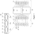
- FIG. 1 depicts a photonic switch structure 100 including a photonic switch 102 and a plurality of polarization controllers 104.
- the photonic switch 102 comprises a plurality of inputs that can be switched to a plurality of outputs.
- the photonic switch 102 comprises a number of input switching cells 112 that can switch an incoming signal to an appropriate switching plane 114a, 114b, or section of a single switching plane, that in turn establishes a connection to an appropriate output switching cell 116 in order to establish the desired connection.
- an appropriate switching plane 114a, 114b, or section of a single switching plane that in turn establishes a connection to an appropriate output switching cell 116 in order to establish the desired connection.
- 8x8 switch architecture for establishing connections between 8 inputs and 8 outputs is shown in Figure 1
- the switches are generally formed from a plurality of individual switching cells.
- the individual switching cells may be provided by a Mach-Zender Interferometer (MZI) structure comprising a pair of
- the MZI structure may function best with a specific polarization of light.
- the individual switching cells may function primarily with transverse electric (TE) polarization.
- TE transverse electric
- TM transverse magnetic
- inputs to the switch 102 may be associated with polarization controllers 104 that convert an optical signal having both a TM polarization component (106) and a TE polarization component (108) to a signal having a single polarization component, such as a TE polarization component (110).
- the polarization controllers 104 are separate components that add to the insertion loss, increase the component count and increase the complexity of the photonic switch structure 100.
- polarization controller architectures are possible depending on the requirements, such as endless, or reset-free, control as well as the ability to adjust any incoming polarization to any output polarization.
- the polarization controllers may be provided as a number of cascaded stages. Depending upon the number of stages cascaded together, a different degree of flexibility of the polarization controller may be provided.
- Figure 1 depicts a 3-stage polarization controller 104a that is capable of producing a specific polarization from any input polarization without requiring resets - a capability referred to herein as "endless polarization control".
- the polarization controller 104a comprises a polarization beam splitter and rotator 118 that splits an incoming beam into orthogonally polarized components and rotates one of the polarized components.
- a series of cascaded phase shifter arms 120a, 120b, 124a, 124b, 128a, 128b and 3dB MMI couplers/splitters 122, 126, 130 allow the unknown polarization to be changed to a particular polarization, such as the TE polarization.
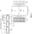
- FIG. 2 depicts a photonic switch incorporating polarization controllers.
- the photonic switch 200 comprises a number of input stages 202 that each have an optical input for receiving an optical signal to be coupled to one of a plurality of output stages 206.
- Optical paths are established between the input stages 202 and output stages 206 through a plurality of intermediary switching stages 204.
- the particular arrangement of the input stages 202, intermediary switching stages 204 and the output stages 206 will depend upon the switch architecture; however, the input stages 202 will typically include one or more optical switches provided by a Mach-Zender Interferometer (MZI) structure for selectively coupling the input optical signal to a particular one of the intermediary switching cells.
- MZI Mach-Zender Interferometer
- the intermediary switching cells may be arranged into one or more similar switching planes 204a, 204b.
- the switch 200 is depicted as being an 8x8, non-blocking switch comprising 2 switching planes each provided by a blocking 8x8 switching plane. Regardless of the particular architecture of the switch 200, it is provided by a number of interconnected silicon photonic components, which operate with a particular polarization. Accordingly, in order to provide efficient switching of the optical signals, the input optical signal should be of the particular optical polarization, such as TE polarization.
- the switch 200 incorporates polarization controllers into the input stages 202 of the switch, providing a compact and efficient switch capable of receiving randomly polarized optical signals and converting the incoming signals to the appropriate polarization for the silicon photonic components.
- each of the input stages 202 comprises a state of polarization (SOP) controller 208 that overlaps with the first input stage 210 of the switching cell. That is, the first input switching stages 202 also provide a last stage of the polarization controller 208. By overlapping the polarization controller 208 with the first stage of the switch input 210, lower insertion loss and power consumption are possible.
- SOP state of polarization
- FIG. 2 depicts details of a polarization controller 208 incorporated into the input stage 202a of the switch.
- the polarization controller 208 comprise a 3 stage polarization controller that can convert an unknown polarization of incoming light to a particular polarization, without requiring the polarization controller to be reset.
- the polarization controller 208 comprises a polarization rotator splitter (PRS) 212 that splits the incoming polarized light into orthogonal polarization components.
- PRS polarization rotator splitter
- the PRS 212 may also rotate the polarization of one of the components by 90° so that it is parallel to polarization of the other polarization component.
- the polarization controller 208 comprise comprises 3 phase shifter stages 214a,214b, 218a, 218b, 222a, 222b that are coupled to 3dB multimode interferometer (MMI) couplers 216, 220, 224.
- the phase shifter stages 214a,214b, 218a, 218b, 222a, 222b are depicted as being cascaded together to the PRS 212 components located in each of two different arms connected to the MMI couplers 216, 220, 224.
- the final stage of the polarization controller also acts as the first stage of the switch matrix. That is, the final stage of the polarization controller may be provided by an optical mixer stage that also provides the first switching stage.
- the output of the final 3dB MMI coupler 224 may be controlled so that all of the optical power of the input signal is transferred to only one of the two outputs of the coupler depending upon the particular routing required by the switch.
- the last stage of the polarization controller incorporates the first stage of the switch matrix.
- the combined last stage of the switch is provided by an MZI structure composed of a pair of phase shifters 222a, 22b located in different arms of the MZI structure and connected to an MMI coupler 224 for combining the phase shifted signals in the two arms.
- the photonic switch 200 depicted in Figure 2 has a multi-plane architecture; however, polarization controllers incorporated into input stages may be used with different switch architectures.
- the different switch architectures may be based on, for example, crossbar architectures, Benes architectures, dilated Banyan architectures, etc.
- the photonic switch 200 is depicted as a space switch that can selectively establish optical paths between a plurality of inputs and a plurality of outputs.
- the photonic switch may alternatively be a tunable filter switch.
- Such tunable filter switches may be used in applications such as reconfigurable add/drop optical network switches, and in optical filters that are used to filter out unwanted signal components such as a sideband to create a single sideband signal.
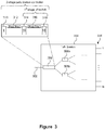
- Figure 3 depicts a 1xN switching cell incorporating a polarization controller.
- the input stages 202 described above with reference to Figure 2 comprised a 1 ⁇ 2 switch incorporating a 3-stage polarization controller with the last stage of the polarization controller being provided by the 1x2 switch.
- 1xN switches 300 may incorporate polarization controllers.
- the 1xN switch 300 switches an input 302 to one of a plurality of outputs 304. The switching is accomplished by a number of individual switching cells arranged together.
- the 1xN switch comprises an input stage 306 that incorporates the polarization controller, which is depicted as being provided by a 2-stage polarization controller.
- the input stage In addition to controlling the polarization of the input, the input stage also switches the input signal, or rather the polarization adjusted input signal, to one of two further individual switching cells 308a, 308b.
- the number of individual switching cells required in a 1xN switch will depend upon the number of outputs, N as well as the switch architecture used. Assuming that the 1xN switch is provided by 1x2 individual switching cells, there may be, depending upon the particular switch architecture, log 2 (N) stages of switching cells.
- the input stage 306 of the 1xN switch comprises a polarization rotator splitter 310 that splits an incoming beam into orthogonal polarization components and rotates the polarization of one of the split beams by 90°.
- the two split beams are provided to different arms of an MZI structure.
- the polarization controller may comprise phase shifters in each arm of the MZI structure.
- the polarization controller of the input stage 306 may include phase shifters 312, 316 in only one arm of the MZI structure.
- the different arms of the MZI structure are coupled to 3dB MMI couplers 314, 318.
- the plurality of phase shifters 312, 316 and couplers 314, 318 provide a plurality of stages cascaded together to the PRS input element 310.
- the final stage of the polarization controller incorporates the first switching stage of the 1xN switch. That is the final stage of the polarization controller is capable of directing the polarization corrected signal to one of two paths, which are coupled to optical switching cells 308a, 308b.
- Figure 4 depicts an input stage of a switching cell incorporating an N-stage polarization controller.
- the figures above have described 3-stage and 2-stage polarization controllers incorporated into switching cell input stages.
- the input stage 400 incorporates an N-stage polarization controller.
- the input stage 400 may be used as the first stage of a photonic switch matrix.
- the input stage 400 incorporates an N-stage polarization controller including an input element, depicted as a polarization rotator and splitter (PRS) 402, that splits an incoming beam into orthogonally polarized components.
- PRS polarization rotator and splitter
- a plurality, N, of polarization controller stages, 404, 406, 408 are cascaded together to the polarization components output from the PRS input element 402.
- the N stage polarization controller comprises a first stage 404 connected to the PRS input element 402, optional one or more additional polarization controller stages 406 cascaded together to the first polarization controller stage 404 and a last polarization controller stage 408 cascaded to the additional polarization controller stages 406, or directly to the first stage 404 if the polarization controller only has two stages.
- the last polarization controller stage 408 can selectively direct the polarization adjusted output beam to one of two outputs of the last polarization controller stage 408.
- the last polarization stage 408 also incorporates the first input switching stage of the switch matrix that the input stage 400 is part of. That is, the last polarization stage 408 also functions as the first input switching stage of the switch matrix, which may reduce insertion losses and optical power consumption of the switch matrix.
- the individual polarization controller stages comprise phase shifters 410a, 410b, 414a, 414b arranged in opposing arms of an MZI structure with 3dB MMI couplers 412, 416 combining the phase shifted signals in opposing arms and joining the stages 404, 406, 408 together.
- the phase shifters 410a, 410b, 414a, 414b are capable of adjusting a relative phase shift between optical signals in opposing arms of the input stage 400.
- the relative phase shift may be achieved using two, or more if desired, phase shifters as depicted in Figure 4 .
- a single phase shifter may be used in one of the two arms, such as phase shifters 410a, 414a for the first and last stages 404, 408.
- Figure 5 depicts an input stage for a switch matrix incorporating a 2-stage polarization controller having a separate beam splitter.
- the above input stages incorporating polarization control described with reference to Figures 2 to 4 have depicted implementing the polarization rotator and splitter (PRS) element on the same chip as the other photonic components of the input stage.
- PRS polarization rotator and splitter
- the input stage 500 for a switch matrix it is possible for the input stage 500 for a switch matrix to include a polarization rotator and splitter provided as an off-chip component 502.
- the on-chip components of the input stage 500 are similar to those described above with regard to Figures 2 to 4 .
- the on-chip components 504 comprise a 1 st stage of a polarization controller 506, optional additional stages of the polarization controller 508 and the combined last stage of the polarization controller and the first stage of the switch matrix 510.
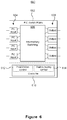
- FIG. 6 depicts a switch based on the switch matrix incorporating an application of photonic switches incorporating polarization controllers.
- the switch 600 may comprise a photonic integrated circuit switch matrix 602 that is manufactured using SOI techniques.
- the switch matrix 602 is depicted as a 4x4 switch, although different sizes of switches are possible.
- the switch matrix 602 is capable of selectively establishing optical paths between the inputs 604 and outputs 608 via the intermediary switching components 606.
- the inputs 604 incorporate polarization controllers as described above.
- the switch 600 may also comprise a controller 610 for controlling the operation of the switch matrix 602.
- the controller 610 may be implemented as an application specific integrated circuit (ASIC), field programmable gate array (FPGA), microprocessor or microcontroller, for example.
- the controller 610 may be implemented on the same chip as the photonic integrated circuit switch matrix 602, or may be implemented on a separate chip.
- the controller 610 provides polarization functionality 612 for controlling the polarization of input signals as well as switch routing functionality 614 for establishing the desired optical paths through the switch matrix 602.
- the switch routing functionality 614 may utilize various different approaches for determining the routing of signals through the switch matrix. Although depicted as distinct functionality, the polarization functionality and the switch routing functionality are combined in the polarization controller.
- the polarization controller functions as a first stage of the switch, providing both a switching function between one of two outputs of the polarization controller, and a polarization controlling function in the currently selected output of the polarization controller.
- the controller 610 may receive various feedback signals in order to perform the polarization control functionality as well as the switch routing.
- the controller 610 may receive an indication of desired optical paths to be established, such as connection of a first input to a fourth output, etc.
- the polarization control may receive measurements or signals from different parts of the polarization controller in order to provide an indication of the state of polarization of the incoming signal.
- the measurements or signals may be provided through various optical taps on the optical path at various locations in the polarization controller of the polarization controlling inputs 602.
- the control algorithms applied to the polarization controllers may vary depending upon the number of stages present in the polarization controller, whether or not the polarization control is reset-free or may require periodic resets, the measurements along the optical path that are available as well as other factors.
- the above has described various implementations for an input stage for a switch matrix that incorporates a polarization controller.
- the switch matrix with incorporated polarization controllers may be implemented as a silicon on insulator (SOI) photonic apparatus providing all-optical switching of signals.
- SOI silicon on insulator
- the incorporation of the polarization controller into the switch inputs provides a polarization independent optical switch in an SOI photonic circuit.
- the switch matrix incorporating polarization controllers works with light in which information is not carried by the polarization.
- the specific photonic components used in the switch matrix with integrated polarization controllers may vary.
- the input component that splits an incoming beam into orthogonal polarization components may be provided by an on-chip component such as a polarization rotator splitter (PRS), a polarization-splitting surface grating coupler, or may be provided off-chip by a polarization beam splitter cube.
- the phase shifters within the MZI switch cell structures may be provided, for example, by thermo-optic switches or carrier injection switches.
- the 3dB MMI couplers described above may be replaced with alternative couplers, such as symmetric directional couplers, adiabatic couplers, etc.
- each architecture typically includes an initial 1xN input switch stage, as opposed to, for example a 2x2 switch.
- the 1xN input switch stage may be replaced with the input stage incorporating the polarization controller as described above.
- the polarization controller may provide endless polarization adjustment or may require a reset.
- a photonic circuit providing a switch matrix incorporating polarization controller inputs as described above may be used in various applications such as all optical switches that switch non-coherent signals, or signals to be detected by non-coherent receivers. Although different applications will be apparent to one of ordinary skill in the art, examples of possible applications may include, for example, datacenter packet switching applications and high-throughput computing applications.
- An optical switch based on the switch matrix incorporating polarization controller inputs as described above may be manufactured on a SOI platform and provide an optical switch having lower insertion loss and power consumption, compared to a switch without incorporated polarization controllers
Landscapes
- Physics & Mathematics (AREA)
- General Physics & Mathematics (AREA)
- Optics & Photonics (AREA)
- Nonlinear Science (AREA)
- Mathematical Physics (AREA)
- Engineering & Computer Science (AREA)
- Computer Networks & Wireless Communication (AREA)
- Optical Modulation, Optical Deflection, Nonlinear Optics, Optical Demodulation, Optical Logic Elements (AREA)
Claims (10)
- Photonische Schaltmatrix, umfassend:eine Mehrzahl von 1×2-Eingangsschaltern (102), wobei jeder 1×2-Eingangsschalter umfasst:einen Eingangsanschluss zum Empfangen eines optischen Strahls;erste und zweite Ausgangsanschlüsse zum Ausgeben des optischen Strahls in einem vordefinierten Polarisationszustand;eine Polarisationssteuerung (104), die mit dem Eingangsanschluss zum Bereitstellen des vordefinierten Polarisationszustands des optischen Strahls gekoppelt ist, wobei die Polarisationssteuerung mindestens eine Polarisationssteuerungsstufe umfasst, die zwei optische Pfade umfasst, die mit zwei Polarisationsanteilen des optischen Strahls assoziiert sind; undeine optische Mischerstufe, die mit den zwei optischen Pfaden der mindestens einen Polarisationssteuerungsstufe zum Mischen von Licht in den zwei optischen Pfaden gekoppelt ist, um den optischen Strahl in dem vordefinierten Polarisationszustand zu dem ersten oder zweiten Ausgangsanschluss zu leiten;eine Mehrzahl von Ausgangsschaltern; undeine Mehrzahl von dazwischenliegenden Schaltern, die mit der Mehrzahl von 1x2-Eingangsschaltern und der Mehrzahl von Ausgangsschaltern zum gezielten Herstellen von optischen Pfaden zwischen der Mehrzahl von 1×2-Eingangsschaltern und der Mehrzahl von Ausgangsschaltern gekoppelt sind, wobei jeder der Mehrzahl von 1x2-Eingangsschaltern ferner umfasst:
ein Eingangselement zum Teilen des Eingangsstrahls in die orthogonalen Polarisationsanteile,wobei das Eingangselement eines von Folgendem umfasst:einen Polarisationsrotator/-teiler (118); undeinen polarisationsteilenden Oberflächengitterkoppler. - Photonische Schaltmatrix nach Anspruch 1, wobei jede der mindestens einen Polarisationssteuerungsstufen und der optischen Mischerstufe eine Mach-Zehnder-Interferometer, MZI,-Struktur mit mindestens einem Phasenschieber umfasst, die in Armen der MZI-Struktur angeordnet ist, die mit einem Koppler verbunden sind.
- Photonische Schaltmatrix nach Anspruch 2, wobei einer oder mehrere der Koppler der mindestens einen Polarisationssteuerungsstufen und der optischen Mischerstufe eines von Folgendem umfasst:einen symmetrischen Richtkoppler;einen adiabatischen Koppler; undeinen Multimode-Interferenz, MMI,-Koppler.
- Photonische Schaltmatrix nach Anspruch 2 oder 3, wobei einer oder mehrere der Phasenschieber der mindestens einen Polarisationssteuerungsstufen und der optischen Mischerstufe eines von Folgendem umfasst:einen thermooptischen Phasenschieber; undeinen Trägerinjektions-Phasenschieber.
- Photonische Schaltmatrix nach Anspruch 1, wobei eine Kombination der Polarisationssteuerung und der optischen Mischerstufe eine 2-stufige Polarisationssteuerung bereitstellt, und die Polarisationssteuerung und die optische Mischerstufe jedes der Mehrzahl von 1×2-Eingangsschaltern umfassen:einen Phasenschieber, der in einem von zwei Armen einer ersten Mach-Zehnder-Interferometer, MZI,-Struktur angeordnet ist, wobei die zwei Arme der ersten MZI-Struktur mit den optischen Pfaden gekoppelt sind, die mit den orthogonalen Polarisationsanteilen assoziiert sind;einen ersten optischen Koppler, der mit den zwei Armen der ersten MZI-Struktur verbunden ist, der zwei optische Ausgangspfade bereitstellt;mindestens einen Phasenschieber, der in einem von zwei Armen einer zweiten MZI-Struktur angeordnet ist, wobei die zwei Arme der zweiten MZI-Struktur mit den zwei optischen Ausgangspfaden des ersten optischen Kopplers gekoppelt sind; undeinen zweiten optischen Koppler, der mit den zwei Armen der zweiten MZI-Struktur verbunden ist, der zwei optische Ausgangspfade bereitstellt.
- Photonische Schaltmatrix nach Anspruch 1, wobei eine Kombination der Polarisationssteuerung und der optischen Mischerstufe eine 3-stufige Polarisationssteuerung bereitstellt, und die Polarisationssteuerung und die optische Mischerstufe jedes der Mehrzahl von 1×2-Eingangsschaltern umfassen:mindestens einen Phasenschieber, der in einem von zwei Armen einer ersten Mach-Zehnder-Interferometer, MZI,-Struktur angeordnet ist, wobei die zwei Arme der ersten MZI-Struktur mit den optischen Pfaden gekoppelt sind, die mit den orthogonalen Polarisationsanteilen assoziiert sind;einen ersten optischen Koppler, der mit den zwei Armen der ersten MZI-Struktur verbunden ist, der zwei optische Ausgangspfade bereitstellt;mindestens einen Phasenschieber, der in einem von zwei Armen einer zweiten MZI-Struktur angeordnet ist, wobei die zwei Arme der zweiten MZI-Struktur mit den zwei optischen Ausgangspfaden des ersten optischen Kopplers gekoppelt sind;einen zweiten optischen Koppler, der mit den zwei Armen der zweiten MZI-Struktur verbunden ist, der zwei optische Ausgangspfade bereitstellt;mindestens einen Phasenschieber, der in einem von zwei Armen einer dritten MZI-Struktur angeordnet ist, wobei die zwei Arme der dritten MZI-Struktur mit den zwei optischen Ausgangspfaden des zweiten optischen Kopplers gekoppelt sind; undeinen dritten optischen Koppler, der mit den zwei Armen der dritten MZI-Struktur verbunden ist, der zwei optische Ausgangspfade bereitstellt.
- Photonische Schaltmatrix nach Anspruch 1, wobei eine Kombination der Polarisationssteuerung und der optischen Mischerstufe eine 4-stufige Polarisationssteuerung bereitstellt, und die Polarisationssteuerung und die optische Mischerstufe jedes der Mehrzahl von 1×2-Eingangsschaltern umfassen:mindestens einen Phasenschieber, der in einem von zwei Armen einer ersten Mach-Zehnder-Interferometer, MZI,-Struktur angeordnet ist, wobei die zwei Arme der ersten MZI-Struktur mit den optischen Pfaden gekoppelt sind, die mit den orthogonalen Polarisationsanteilen assoziiert sind;einen ersten optischen Koppler, der mit den zwei Armen der ersten MZI-Struktur verbunden ist, der zwei optische Ausgangspfade bereitstellt;mindestens einen Phasenschieber, der in einem von zwei Armen einer zweiten MZI-Struktur angeordnet ist, wobei die zwei Arme der zweiten MZI-Struktur mit den zwei optischen Ausgangspfaden des ersten optischen Kopplers gekoppelt sind;einen zweiten optischen Koppler, der mit den zwei Armen der zweiten MZI-Struktur verbunden ist, der zwei optische Ausgangspfade bereitstellt;mindestens einen Phasenschieber, der in einem von zwei Armen einer dritten MZI-Struktur angeordnet ist, wobei die zwei Arme der dritten MZI-Struktur mit den zwei optischen Ausgangspfaden des zweiten optischen Kopplers gekoppelt sind;einen dritten optischen Koppler, der mit den zwei Armen der dritten MZI-Struktur verbunden ist, der zwei optische Ausgangspfade bereitstellt;mindestens einen Phasenschieber, der in einem von zwei Armen einer vierten MZI-Struktur angeordnet ist, wobei die zwei Arme der vierten MZI-Struktur mit den zwei optischen Ausgangspfaden des dritten optischen Kopplers gekoppelt sind; undeinen vierten optischen Koppler, der mit den zwei Armen der vierten MZI-Struktur verbunden ist, der zwei optische Ausgangspfade bereitstellt.
- Photonische Schaltmatrix nach einem der Ansprüche 1 bis 7, wobei die photonische Schaltmatrix ferner eine Steuerung umfasst;
wobei die Steuerung zum Steuern einer Polarisation der Eingangsstrahlen, die mit jedem der 1×2-Schalter assoziiert sind, und zum Routen von optischen Pfaden durch die Schaltmatrix dient. - Photonische Schaltmatrix nach Anspruch 8, wobei die Steuerung und die photonische Schaltmatrix auf einem einzelnen "Silicon-on-Insulator", SOI,-Chip implementiert sind.
- Photonische Schaltmatrix nach einem der Ansprüche 1 bis 9, ferner umfassend eine Mehrzahl von Polarisationsrotator-und-teiler, PRS,-Elementen, die chipextern von der Schaltmatrix angeordnet sind, wobei jedes der Mehrzahl von PRS-Elementen mit einem jeweiligen der 1x2-Eingangsschalter assoziiert ist.
Applications Claiming Priority (2)
| Application Number | Priority Date | Filing Date | Title |
|---|---|---|---|
| US15/095,746 US9784921B1 (en) | 2016-04-11 | 2016-04-11 | Switch matrix incorporating polarization controller |
| PCT/CN2016/079578 WO2017177472A1 (en) | 2016-04-11 | 2016-04-18 | Switch matrix incorporating polarization controller |
Publications (3)
| Publication Number | Publication Date |
|---|---|
| EP3417554A1 EP3417554A1 (de) | 2018-12-26 |
| EP3417554A4 EP3417554A4 (de) | 2019-02-27 |
| EP3417554B1 true EP3417554B1 (de) | 2021-12-29 |
Family
ID=59981340
Family Applications (1)
| Application Number | Title | Priority Date | Filing Date |
|---|---|---|---|
| EP16898289.0A Active EP3417554B1 (de) | 2016-04-11 | 2016-04-18 | Schaltmatrix mit polarisationssteuergerät |
Country Status (4)
| Country | Link |
|---|---|
| US (1) | US9784921B1 (de) |
| EP (1) | EP3417554B1 (de) |
| JP (1) | JP6969849B2 (de) |
| WO (1) | WO2017177472A1 (de) |
Families Citing this family (4)
| Publication number | Priority date | Publication date | Assignee | Title |
|---|---|---|---|---|
| CN112970210B (zh) * | 2018-11-24 | 2022-07-22 | 华为技术有限公司 | 偏振处理装置、光收发机和光偏振处理的方法 |
| EP3974813B1 (de) * | 2020-09-28 | 2024-07-17 | IMEC vzw | System zur kompensation der optischen ausrichtung für ein gasdetektionssystem |
| CN113300724B (zh) * | 2021-05-14 | 2022-02-15 | 电子科技大学 | 一种开关矩阵多波束组件及开关矩阵多波束扩展式组件 |
| CN120507928B (zh) * | 2025-07-22 | 2025-10-17 | 赛丽科技(苏州)有限公司 | 一种偏振控制芯片及系统、控制方法 |
Family Cites Families (15)
| Publication number | Priority date | Publication date | Assignee | Title |
|---|---|---|---|---|
| US5751868A (en) * | 1995-07-03 | 1998-05-12 | Bell Communications Research, Inc. | Asymetrically dilated optical cross connect switches |
| JP4078898B2 (ja) * | 2002-06-28 | 2008-04-23 | 日本電気株式会社 | 熱光学位相シフタ及びその製造方法 |
| US7006732B2 (en) * | 2003-03-21 | 2006-02-28 | Luxtera, Inc. | Polarization splitting grating couplers |
| JP2007003708A (ja) * | 2005-06-22 | 2007-01-11 | Ricoh Co Ltd | 光集積回路 |
| JP2009192809A (ja) * | 2008-02-14 | 2009-08-27 | Fujitsu Ltd | 光処理装置および光処理方法 |
| US7822298B2 (en) | 2008-04-15 | 2010-10-26 | Alcatel-Lucent Usa Inc. | Polarization component processor, method of processing polarization components and integrated photonic circuit employing the same |
| US20120002971A1 (en) * | 2010-06-30 | 2012-01-05 | Alcatel-Lucent Usa Inc. | Polarization-tracking device having a waveguide-grating coupler |
| US9432750B1 (en) * | 2013-04-19 | 2016-08-30 | Wavexing, Inc. | Contentionless N×M wavelength cross connect |
| US20150043905A1 (en) | 2013-08-07 | 2015-02-12 | Futurewei Technologies, Inc. | System and Method for Photonic Switching and Controlling Photonic Switching in a Data Center |
| US9244227B2 (en) * | 2013-11-11 | 2016-01-26 | Futurewei Technologies, Inc. | Polarization splitter/combiner based on a one-dimensional grating coupler |
| WO2015124952A1 (en) * | 2014-02-24 | 2015-08-27 | Rockley Photonics Limited | Detector remodulator and optoelectronic switch |
| JP2015219276A (ja) * | 2014-05-14 | 2015-12-07 | 日本電信電話株式会社 | 偏波分離回路 |
| EP3035113A4 (de) * | 2014-05-23 | 2016-08-10 | Huawei Tech Co Ltd | Polarisationssteuerungsvorrichtung und polarisationssteuerungsverfahren |
| US9746700B2 (en) * | 2014-07-08 | 2017-08-29 | Cisco Technology, Inc. | Silicon photonic hybrid polarization demultiplexer |
| US20160057516A1 (en) | 2014-08-21 | 2016-02-25 | Coriant Advanced Technology, LLC | Transceivers for signal switching architecture |
-
2016
- 2016-04-11 US US15/095,746 patent/US9784921B1/en active Active
- 2016-04-18 WO PCT/CN2016/079578 patent/WO2017177472A1/en not_active Ceased
- 2016-04-18 JP JP2018548877A patent/JP6969849B2/ja active Active
- 2016-04-18 EP EP16898289.0A patent/EP3417554B1/de active Active
Also Published As
| Publication number | Publication date |
|---|---|
| US9784921B1 (en) | 2017-10-10 |
| JP6969849B2 (ja) | 2021-11-24 |
| US20170293086A1 (en) | 2017-10-12 |
| JP2019511008A (ja) | 2019-04-18 |
| EP3417554A4 (de) | 2019-02-27 |
| EP3417554A1 (de) | 2018-12-26 |
| WO2017177472A1 (en) | 2017-10-19 |
Similar Documents
| Publication | Publication Date | Title |
|---|---|---|
| Stabile et al. | Integrated optical switch matrices for packet data networks | |
| US8121478B2 (en) | Method and apparatus for implementing non-blocking computer interconnection network using bidirectional optical switch | |
| EP2976846B1 (de) | Wellenlängenselektiver schalter mit integrierter kanalüberwachung | |
| US9794656B2 (en) | Modular photonic switch architecture | |
| US9084033B2 (en) | Optical cross-connect apparatus | |
| EP3417554B1 (de) | Schaltmatrix mit polarisationssteuergerät | |
| JP6533743B2 (ja) | 光クロスコネクト装置 | |
| Bahadori et al. | Loss and crosstalk of scalable MZI-based switch topologies in silicon photonic platform | |
| US10911844B2 (en) | Integrated high-radix non-blocking optical switching fabric | |
| Hop et al. | Design of silicon TE0/TE1 mode router using Mach-Zehnder and multimode interferometers | |
| US20010038735A1 (en) | Apparatus and method for wavelength selective switching | |
| Wu et al. | Large-port-count MEMS silicon photonics switches | |
| WO2012137555A1 (ja) | 導波路型光スイッチ | |
| Williams | Integrated semiconductor-optical-amplifier-based switch fabrics for high-capacity interconnects | |
| Zhang et al. | LOOP: A low-loss compact plasmonic router for ONoC | |
| Wu et al. | Monolithic large-scale optical switches using silicon photonic MEMS | |
| Hino et al. | Transponder aggregator based on silicon photonics technologies for next generation CDC-ROADM systems | |
| Blatter et al. | 2x4 Spatial Switch Exploiting On-Chip Beam Steering | |
| He et al. | A hitless and gridless wavelength selective switch for versatile spectral shapings | |
| Raponi et al. | Heterogeneous space switches for power-efficient optical interconnection networks | |
| WO2016002736A1 (ja) | 光クロスコネクト装置 | |
| Hunter | Planar optical space switch architectures | |
| Nakata et al. | A new pair-controlled photonic switch matrix | |
| Shoji et al. | Si-wire optical switch enabling three possible cross-connections among four ports |
Legal Events
| Date | Code | Title | Description |
|---|---|---|---|
| STAA | Information on the status of an ep patent application or granted ep patent |
Free format text: STATUS: THE INTERNATIONAL PUBLICATION HAS BEEN MADE |
|
| PUAI | Public reference made under article 153(3) epc to a published international application that has entered the european phase |
Free format text: ORIGINAL CODE: 0009012 |
|
| STAA | Information on the status of an ep patent application or granted ep patent |
Free format text: STATUS: REQUEST FOR EXAMINATION WAS MADE |
|
| 17P | Request for examination filed |
Effective date: 20180919 |
|
| AK | Designated contracting states |
Kind code of ref document: A1 Designated state(s): AL AT BE BG CH CY CZ DE DK EE ES FI FR GB GR HR HU IE IS IT LI LT LU LV MC MK MT NL NO PL PT RO RS SE SI SK SM TR |
|
| AX | Request for extension of the european patent |
Extension state: BA ME |
|
| REG | Reference to a national code |
Ref country code: DE Ref legal event code: R079 Ref document number: 602016067964 Country of ref document: DE Free format text: PREVIOUS MAIN CLASS: H04B0010250000 Ipc: H04Q0011000000 |
|
| A4 | Supplementary search report drawn up and despatched |
Effective date: 20190128 |
|
| RIC1 | Information provided on ipc code assigned before grant |
Ipc: H04B 10/25 20130101ALI20190122BHEP Ipc: H04Q 11/00 20060101AFI20190122BHEP Ipc: H04B 10/70 20130101ALI20190122BHEP |
|
| DAV | Request for validation of the european patent (deleted) | ||
| DAX | Request for extension of the european patent (deleted) | ||
| GRAP | Despatch of communication of intention to grant a patent |
Free format text: ORIGINAL CODE: EPIDOSNIGR1 |
|
| STAA | Information on the status of an ep patent application or granted ep patent |
Free format text: STATUS: GRANT OF PATENT IS INTENDED |
|
| INTG | Intention to grant announced |
Effective date: 20210803 |
|
| GRAS | Grant fee paid |
Free format text: ORIGINAL CODE: EPIDOSNIGR3 |
|
| GRAA | (expected) grant |
Free format text: ORIGINAL CODE: 0009210 |
|
| STAA | Information on the status of an ep patent application or granted ep patent |
Free format text: STATUS: THE PATENT HAS BEEN GRANTED |
|
| AK | Designated contracting states |
Kind code of ref document: B1 Designated state(s): AL AT BE BG CH CY CZ DE DK EE ES FI FR GB GR HR HU IE IS IT LI LT LU LV MC MK MT NL NO PL PT RO RS SE SI SK SM TR |
|
| REG | Reference to a national code |
Ref country code: GB Ref legal event code: FG4D |
|
| REG | Reference to a national code |
Ref country code: CH Ref legal event code: EP |
|
| REG | Reference to a national code |
Ref country code: DE Ref legal event code: R096 Ref document number: 602016067964 Country of ref document: DE |
|
| REG | Reference to a national code |
Ref country code: AT Ref legal event code: REF Ref document number: 1459581 Country of ref document: AT Kind code of ref document: T Effective date: 20220115 |
|
| REG | Reference to a national code |
Ref country code: IE Ref legal event code: FG4D |
|
| REG | Reference to a national code |
Ref country code: LT Ref legal event code: MG9D |
|
| PG25 | Lapsed in a contracting state [announced via postgrant information from national office to epo] |
Ref country code: RS Free format text: LAPSE BECAUSE OF FAILURE TO SUBMIT A TRANSLATION OF THE DESCRIPTION OR TO PAY THE FEE WITHIN THE PRESCRIBED TIME-LIMIT Effective date: 20211229 Ref country code: LT Free format text: LAPSE BECAUSE OF FAILURE TO SUBMIT A TRANSLATION OF THE DESCRIPTION OR TO PAY THE FEE WITHIN THE PRESCRIBED TIME-LIMIT Effective date: 20211229 Ref country code: FI Free format text: LAPSE BECAUSE OF FAILURE TO SUBMIT A TRANSLATION OF THE DESCRIPTION OR TO PAY THE FEE WITHIN THE PRESCRIBED TIME-LIMIT Effective date: 20211229 Ref country code: BG Free format text: LAPSE BECAUSE OF FAILURE TO SUBMIT A TRANSLATION OF THE DESCRIPTION OR TO PAY THE FEE WITHIN THE PRESCRIBED TIME-LIMIT Effective date: 20220329 |
|
| REG | Reference to a national code |
Ref country code: NL Ref legal event code: MP Effective date: 20211229 |
|
| REG | Reference to a national code |
Ref country code: AT Ref legal event code: MK05 Ref document number: 1459581 Country of ref document: AT Kind code of ref document: T Effective date: 20211229 |
|
| PG25 | Lapsed in a contracting state [announced via postgrant information from national office to epo] |
Ref country code: SE Free format text: LAPSE BECAUSE OF FAILURE TO SUBMIT A TRANSLATION OF THE DESCRIPTION OR TO PAY THE FEE WITHIN THE PRESCRIBED TIME-LIMIT Effective date: 20211229 Ref country code: NO Free format text: LAPSE BECAUSE OF FAILURE TO SUBMIT A TRANSLATION OF THE DESCRIPTION OR TO PAY THE FEE WITHIN THE PRESCRIBED TIME-LIMIT Effective date: 20220329 Ref country code: LV Free format text: LAPSE BECAUSE OF FAILURE TO SUBMIT A TRANSLATION OF THE DESCRIPTION OR TO PAY THE FEE WITHIN THE PRESCRIBED TIME-LIMIT Effective date: 20211229 Ref country code: HR Free format text: LAPSE BECAUSE OF FAILURE TO SUBMIT A TRANSLATION OF THE DESCRIPTION OR TO PAY THE FEE WITHIN THE PRESCRIBED TIME-LIMIT Effective date: 20211229 Ref country code: GR Free format text: LAPSE BECAUSE OF FAILURE TO SUBMIT A TRANSLATION OF THE DESCRIPTION OR TO PAY THE FEE WITHIN THE PRESCRIBED TIME-LIMIT Effective date: 20220330 |
|
| PG25 | Lapsed in a contracting state [announced via postgrant information from national office to epo] |
Ref country code: NL Free format text: LAPSE BECAUSE OF FAILURE TO SUBMIT A TRANSLATION OF THE DESCRIPTION OR TO PAY THE FEE WITHIN THE PRESCRIBED TIME-LIMIT Effective date: 20211229 |
|
| PG25 | Lapsed in a contracting state [announced via postgrant information from national office to epo] |
Ref country code: SM Free format text: LAPSE BECAUSE OF FAILURE TO SUBMIT A TRANSLATION OF THE DESCRIPTION OR TO PAY THE FEE WITHIN THE PRESCRIBED TIME-LIMIT Effective date: 20211229 Ref country code: SK Free format text: LAPSE BECAUSE OF FAILURE TO SUBMIT A TRANSLATION OF THE DESCRIPTION OR TO PAY THE FEE WITHIN THE PRESCRIBED TIME-LIMIT Effective date: 20211229 Ref country code: RO Free format text: LAPSE BECAUSE OF FAILURE TO SUBMIT A TRANSLATION OF THE DESCRIPTION OR TO PAY THE FEE WITHIN THE PRESCRIBED TIME-LIMIT Effective date: 20211229 Ref country code: PT Free format text: LAPSE BECAUSE OF FAILURE TO SUBMIT A TRANSLATION OF THE DESCRIPTION OR TO PAY THE FEE WITHIN THE PRESCRIBED TIME-LIMIT Effective date: 20220429 Ref country code: ES Free format text: LAPSE BECAUSE OF FAILURE TO SUBMIT A TRANSLATION OF THE DESCRIPTION OR TO PAY THE FEE WITHIN THE PRESCRIBED TIME-LIMIT Effective date: 20211229 Ref country code: EE Free format text: LAPSE BECAUSE OF FAILURE TO SUBMIT A TRANSLATION OF THE DESCRIPTION OR TO PAY THE FEE WITHIN THE PRESCRIBED TIME-LIMIT Effective date: 20211229 Ref country code: CZ Free format text: LAPSE BECAUSE OF FAILURE TO SUBMIT A TRANSLATION OF THE DESCRIPTION OR TO PAY THE FEE WITHIN THE PRESCRIBED TIME-LIMIT Effective date: 20211229 |
|
| PG25 | Lapsed in a contracting state [announced via postgrant information from national office to epo] |
Ref country code: PL Free format text: LAPSE BECAUSE OF FAILURE TO SUBMIT A TRANSLATION OF THE DESCRIPTION OR TO PAY THE FEE WITHIN THE PRESCRIBED TIME-LIMIT Effective date: 20211229 Ref country code: AT Free format text: LAPSE BECAUSE OF FAILURE TO SUBMIT A TRANSLATION OF THE DESCRIPTION OR TO PAY THE FEE WITHIN THE PRESCRIBED TIME-LIMIT Effective date: 20211229 |
|
| PG25 | Lapsed in a contracting state [announced via postgrant information from national office to epo] |
Ref country code: IS Free format text: LAPSE BECAUSE OF FAILURE TO SUBMIT A TRANSLATION OF THE DESCRIPTION OR TO PAY THE FEE WITHIN THE PRESCRIBED TIME-LIMIT Effective date: 20220429 |
|
| REG | Reference to a national code |
Ref country code: DE Ref legal event code: R097 Ref document number: 602016067964 Country of ref document: DE |
|
| PG25 | Lapsed in a contracting state [announced via postgrant information from national office to epo] |
Ref country code: DK Free format text: LAPSE BECAUSE OF FAILURE TO SUBMIT A TRANSLATION OF THE DESCRIPTION OR TO PAY THE FEE WITHIN THE PRESCRIBED TIME-LIMIT Effective date: 20211229 Ref country code: AL Free format text: LAPSE BECAUSE OF FAILURE TO SUBMIT A TRANSLATION OF THE DESCRIPTION OR TO PAY THE FEE WITHIN THE PRESCRIBED TIME-LIMIT Effective date: 20211229 |
|
| PLBE | No opposition filed within time limit |
Free format text: ORIGINAL CODE: 0009261 |
|
| STAA | Information on the status of an ep patent application or granted ep patent |
Free format text: STATUS: NO OPPOSITION FILED WITHIN TIME LIMIT |
|
| REG | Reference to a national code |
Ref country code: CH Ref legal event code: PL |
|
| 26N | No opposition filed |
Effective date: 20220930 |
|
| GBPC | Gb: european patent ceased through non-payment of renewal fee |
Effective date: 20220418 |
|
| REG | Reference to a national code |
Ref country code: BE Ref legal event code: MM Effective date: 20220430 |
|
| PG25 | Lapsed in a contracting state [announced via postgrant information from national office to epo] |
Ref country code: MC Free format text: LAPSE BECAUSE OF FAILURE TO SUBMIT A TRANSLATION OF THE DESCRIPTION OR TO PAY THE FEE WITHIN THE PRESCRIBED TIME-LIMIT Effective date: 20211229 Ref country code: LU Free format text: LAPSE BECAUSE OF NON-PAYMENT OF DUE FEES Effective date: 20220418 Ref country code: LI Free format text: LAPSE BECAUSE OF NON-PAYMENT OF DUE FEES Effective date: 20220430 Ref country code: GB Free format text: LAPSE BECAUSE OF NON-PAYMENT OF DUE FEES Effective date: 20220418 Ref country code: FR Free format text: LAPSE BECAUSE OF NON-PAYMENT OF DUE FEES Effective date: 20220430 Ref country code: CH Free format text: LAPSE BECAUSE OF NON-PAYMENT OF DUE FEES Effective date: 20220430 |
|
| PG25 | Lapsed in a contracting state [announced via postgrant information from national office to epo] |
Ref country code: SI Free format text: LAPSE BECAUSE OF FAILURE TO SUBMIT A TRANSLATION OF THE DESCRIPTION OR TO PAY THE FEE WITHIN THE PRESCRIBED TIME-LIMIT Effective date: 20211229 Ref country code: BE Free format text: LAPSE BECAUSE OF NON-PAYMENT OF DUE FEES Effective date: 20220430 |
|
| PG25 | Lapsed in a contracting state [announced via postgrant information from national office to epo] |
Ref country code: IE Free format text: LAPSE BECAUSE OF NON-PAYMENT OF DUE FEES Effective date: 20220418 |
|
| PG25 | Lapsed in a contracting state [announced via postgrant information from national office to epo] |
Ref country code: IT Free format text: LAPSE BECAUSE OF FAILURE TO SUBMIT A TRANSLATION OF THE DESCRIPTION OR TO PAY THE FEE WITHIN THE PRESCRIBED TIME-LIMIT Effective date: 20211229 |
|
| P01 | Opt-out of the competence of the unified patent court (upc) registered |
Effective date: 20230524 |
|
| PG25 | Lapsed in a contracting state [announced via postgrant information from national office to epo] |
Ref country code: HU Free format text: LAPSE BECAUSE OF FAILURE TO SUBMIT A TRANSLATION OF THE DESCRIPTION OR TO PAY THE FEE WITHIN THE PRESCRIBED TIME-LIMIT; INVALID AB INITIO Effective date: 20160418 |
|
| PG25 | Lapsed in a contracting state [announced via postgrant information from national office to epo] |
Ref country code: MK Free format text: LAPSE BECAUSE OF FAILURE TO SUBMIT A TRANSLATION OF THE DESCRIPTION OR TO PAY THE FEE WITHIN THE PRESCRIBED TIME-LIMIT Effective date: 20211229 Ref country code: CY Free format text: LAPSE BECAUSE OF FAILURE TO SUBMIT A TRANSLATION OF THE DESCRIPTION OR TO PAY THE FEE WITHIN THE PRESCRIBED TIME-LIMIT Effective date: 20211229 |
|
| PG25 | Lapsed in a contracting state [announced via postgrant information from national office to epo] |
Ref country code: MT Free format text: LAPSE BECAUSE OF FAILURE TO SUBMIT A TRANSLATION OF THE DESCRIPTION OR TO PAY THE FEE WITHIN THE PRESCRIBED TIME-LIMIT Effective date: 20211229 |
|
| PGFP | Annual fee paid to national office [announced via postgrant information from national office to epo] |
Ref country code: DE Payment date: 20250305 Year of fee payment: 10 |
|
| PG25 | Lapsed in a contracting state [announced via postgrant information from national office to epo] |
Ref country code: TR Free format text: LAPSE BECAUSE OF FAILURE TO SUBMIT A TRANSLATION OF THE DESCRIPTION OR TO PAY THE FEE WITHIN THE PRESCRIBED TIME-LIMIT Effective date: 20211229 |