EP3416183A1 - Substrate treatment method for semiconductor device fabrication - Google Patents
Substrate treatment method for semiconductor device fabrication Download PDFInfo
- Publication number
- EP3416183A1 EP3416183A1 EP18165916.0A EP18165916A EP3416183A1 EP 3416183 A1 EP3416183 A1 EP 3416183A1 EP 18165916 A EP18165916 A EP 18165916A EP 3416183 A1 EP3416183 A1 EP 3416183A1
- Authority
- EP
- European Patent Office
- Prior art keywords
- layer
- metal
- oxide layer
- metal oxide
- germanium
- Prior art date
- Legal status (The legal status is an assumption and is not a legal conclusion. Google has not performed a legal analysis and makes no representation as to the accuracy of the status listed.)
- Granted
Links
Images


Classifications
-
- H—ELECTRICITY
- H10—SEMICONDUCTOR DEVICES; ELECTRIC SOLID-STATE DEVICES NOT OTHERWISE PROVIDED FOR
- H10D—INORGANIC ELECTRIC SEMICONDUCTOR DEVICES
- H10D64/00—Electrodes of devices having potential barriers
- H10D64/01—Manufacture or treatment
- H10D64/013—Manufacture or treatment of electrodes having a conductor capacitively coupled to a semiconductor by an insulator
- H10D64/01356—Manufacture or treatment of electrodes having a conductor capacitively coupled to a semiconductor by an insulator the insulator being formed after the semiconductor body, the semiconductor being a Group IV material and not being silicon, e.g. Ge, SiGe or SiGeC
-
- B—PERFORMING OPERATIONS; TRANSPORTING
- B81—MICROSTRUCTURAL TECHNOLOGY
- B81C—PROCESSES OR APPARATUS SPECIALLY ADAPTED FOR THE MANUFACTURE OR TREATMENT OF MICROSTRUCTURAL DEVICES OR SYSTEMS
- B81C1/00—Manufacture or treatment of devices or systems in or on a substrate
- B81C1/00015—Manufacture or treatment of devices or systems in or on a substrate for manufacturing microsystems
- B81C1/00222—Integrating an electronic processing unit with a micromechanical structure
- B81C1/00238—Joining a substrate with an electronic processing unit and a substrate with a micromechanical structure
-
- H—ELECTRICITY
- H10—SEMICONDUCTOR DEVICES; ELECTRIC SOLID-STATE DEVICES NOT OTHERWISE PROVIDED FOR
- H10D—INORGANIC ELECTRIC SEMICONDUCTOR DEVICES
- H10D64/00—Electrodes of devices having potential barriers
- H10D64/01—Manufacture or treatment
- H10D64/013—Manufacture or treatment of electrodes having a conductor capacitively coupled to a semiconductor by an insulator
- H10D64/01302—Manufacture or treatment of electrodes having a conductor capacitively coupled to a semiconductor by an insulator the insulator being formed after the semiconductor body, the semiconductor being silicon
- H10D64/01332—Making the insulator
- H10D64/0135—Making the insulator by deposition of a layer, e.g. metal, metal compound or polysilicon, followed by transformation thereof into the insulator
-
- H—ELECTRICITY
- H10—SEMICONDUCTOR DEVICES; ELECTRIC SOLID-STATE DEVICES NOT OTHERWISE PROVIDED FOR
- H10D—INORGANIC ELECTRIC SEMICONDUCTOR DEVICES
- H10D64/00—Electrodes of devices having potential barriers
- H10D64/01—Manufacture or treatment
- H10D64/021—Manufacture or treatment using multiple gate spacer layers, e.g. bilayered sidewall spacers
-
- H—ELECTRICITY
- H10—SEMICONDUCTOR DEVICES; ELECTRIC SOLID-STATE DEVICES NOT OTHERWISE PROVIDED FOR
- H10D—INORGANIC ELECTRIC SEMICONDUCTOR DEVICES
- H10D64/00—Electrodes of devices having potential barriers
- H10D64/60—Electrodes characterised by their materials
- H10D64/66—Electrodes having a conductor capacitively coupled to a semiconductor by an insulator, e.g. MIS electrodes
- H10D64/665—Electrodes having a conductor capacitively coupled to a semiconductor by an insulator, e.g. MIS electrodes the conductor comprising a layer of elemental metal contacting the insulator, e.g. tungsten or molybdenum
-
- H—ELECTRICITY
- H10—SEMICONDUCTOR DEVICES; ELECTRIC SOLID-STATE DEVICES NOT OTHERWISE PROVIDED FOR
- H10D—INORGANIC ELECTRIC SEMICONDUCTOR DEVICES
- H10D64/00—Electrodes of devices having potential barriers
- H10D64/60—Electrodes characterised by their materials
- H10D64/66—Electrodes having a conductor capacitively coupled to a semiconductor by an insulator, e.g. MIS electrodes
- H10D64/68—Electrodes having a conductor capacitively coupled to a semiconductor by an insulator, e.g. MIS electrodes characterised by the insulator, e.g. by the gate insulator
- H10D64/691—Electrodes having a conductor capacitively coupled to a semiconductor by an insulator, e.g. MIS electrodes characterised by the insulator, e.g. by the gate insulator comprising metallic compounds, e.g. metal oxides or metal silicates
-
- H—ELECTRICITY
- H10—SEMICONDUCTOR DEVICES; ELECTRIC SOLID-STATE DEVICES NOT OTHERWISE PROVIDED FOR
- H10P—GENERIC PROCESSES OR APPARATUS FOR THE MANUFACTURE OR TREATMENT OF DEVICES COVERED BY CLASS H10
- H10P14/00—Formation of materials, e.g. in the shape of layers or pillars
- H10P14/40—Formation of materials, e.g. in the shape of layers or pillars of conductive or resistive materials
- H10P14/42—Formation of materials, e.g. in the shape of layers or pillars of conductive or resistive materials using a gas or vapour
- H10P14/43—Chemical deposition, e.g. chemical vapour deposition [CVD]
- H10P14/432—Chemical deposition, e.g. chemical vapour deposition [CVD] using selective deposition
-
- H—ELECTRICITY
- H10—SEMICONDUCTOR DEVICES; ELECTRIC SOLID-STATE DEVICES NOT OTHERWISE PROVIDED FOR
- H10P—GENERIC PROCESSES OR APPARATUS FOR THE MANUFACTURE OR TREATMENT OF DEVICES COVERED BY CLASS H10
- H10P14/00—Formation of materials, e.g. in the shape of layers or pillars
- H10P14/60—Formation of materials, e.g. in the shape of layers or pillars of insulating materials
- H10P14/63—Formation of materials, e.g. in the shape of layers or pillars of insulating materials characterised by the formation processes
- H10P14/6302—Non-deposition formation processes
- H10P14/6304—Formation by oxidation, e.g. oxidation of the substrate
- H10P14/6314—Formation by oxidation, e.g. oxidation of the substrate of a metallic layer
-
- H—ELECTRICITY
- H10—SEMICONDUCTOR DEVICES; ELECTRIC SOLID-STATE DEVICES NOT OTHERWISE PROVIDED FOR
- H10P—GENERIC PROCESSES OR APPARATUS FOR THE MANUFACTURE OR TREATMENT OF DEVICES COVERED BY CLASS H10
- H10P14/00—Formation of materials, e.g. in the shape of layers or pillars
- H10P14/60—Formation of materials, e.g. in the shape of layers or pillars of insulating materials
- H10P14/63—Formation of materials, e.g. in the shape of layers or pillars of insulating materials characterised by the formation processes
- H10P14/6302—Non-deposition formation processes
- H10P14/6322—Formation by thermal treatments
-
- H—ELECTRICITY
- H10—SEMICONDUCTOR DEVICES; ELECTRIC SOLID-STATE DEVICES NOT OTHERWISE PROVIDED FOR
- H10P—GENERIC PROCESSES OR APPARATUS FOR THE MANUFACTURE OR TREATMENT OF DEVICES COVERED BY CLASS H10
- H10P14/00—Formation of materials, e.g. in the shape of layers or pillars
- H10P14/60—Formation of materials, e.g. in the shape of layers or pillars of insulating materials
- H10P14/69—Inorganic materials
- H10P14/692—Inorganic materials composed of oxides, glassy oxides or oxide-based glasses
- H10P14/6938—Inorganic materials composed of oxides, glassy oxides or oxide-based glasses the material containing at least one metal element, e.g. metal oxides, metal oxynitrides or metal oxycarbides
- H10P14/6939—Inorganic materials composed of oxides, glassy oxides or oxide-based glasses the material containing at least one metal element, e.g. metal oxides, metal oxynitrides or metal oxycarbides characterised by the metal
- H10P14/69392—Inorganic materials composed of oxides, glassy oxides or oxide-based glasses the material containing at least one metal element, e.g. metal oxides, metal oxynitrides or metal oxycarbides characterised by the metal the material containing hafnium, e.g. HfO2
-
- B—PERFORMING OPERATIONS; TRANSPORTING
- B81—MICROSTRUCTURAL TECHNOLOGY
- B81C—PROCESSES OR APPARATUS SPECIALLY ADAPTED FOR THE MANUFACTURE OR TREATMENT OF MICROSTRUCTURAL DEVICES OR SYSTEMS
- B81C2203/00—Forming microstructural systems
- B81C2203/03—Bonding two components
- B81C2203/033—Thermal bonding
- B81C2203/035—Soldering
-
- H—ELECTRICITY
- H10—SEMICONDUCTOR DEVICES; ELECTRIC SOLID-STATE DEVICES NOT OTHERWISE PROVIDED FOR
- H10W—GENERIC PACKAGES, INTERCONNECTIONS, CONNECTORS OR OTHER CONSTRUCTIONAL DETAILS OF DEVICES COVERED BY CLASS H10
- H10W20/00—Interconnections in chips, wafers or substrates
- H10W20/01—Manufacture or treatment
- H10W20/021—Manufacture or treatment of interconnections within wafers or substrates
- H10W20/023—Manufacture or treatment of interconnections within wafers or substrates the interconnections being through-semiconductor vias
Definitions
- This disclosure relates generally to semiconductor device fabrication, and more specifically, to substrate treatment method for semiconductor device fabrication.
- germanium based CMOS semiconductor devices are often found in a large spectrum of electronic products - from sewing machines to washing machines, from automobiles to cellular telephones, and so on. As technology progresses, these semiconductor devices are expected to reduce in size and cost while increasing performance. However, it is unlikely that traditional silicon (Si) based complementary metal oxide semiconductor (CMOS) technology can continue to drive semiconductor device performance without reaching limits. In pursuit of more advanced semiconductor device performance, germanium (Ge) based CMOS has been gaining favorable attention. One aspect of germanium based CMOS semiconductor devices is the increased mobility of electrons and holes over silicon based CMOS devices. The increased mobility can allow germanium based CMOS to continue advancement of semiconductor device performance.
- a method of forming a structure on a germanium (Ge) substrate to remove a germanium oxide layer By depositing a thin metal layer over a germanium oxide layer at a top surface of a germanium substrate followed by an anneal process, a metal oxide can be formed during the anneal process. The metal oxide formation effectively removes the germanium oxide layer and provides a quality interface layer at the surface of the germanium substrate. With the formation of the metal oxide, a subsequent deposition of a like metal oxide can be used to form a high-K dielectric. Likewise, after formation of the metal oxide, a subsequent deposition of a like metal can be used to form an adhesion layer at a die-on-die interface.
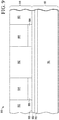
- FIGs. 1-6 illustrate, in simplified cross-sectional views, various stages of manufacture of an exemplary semiconductor device formed in accordance with an embodiment of the present disclosure.
- FIG. 1 illustrates in a simplified cross-sectional view, exemplary semiconductor device 100 at a stage of manufacture in accordance with an embodiment of the present invention.
- exemplary semiconductor device 100 includes a substrate 102 having a germanium oxide (GeOx, where 0 ⁇ x ⁇ 2) layer 104 formed at a top surface of the substrate.
- the substrate 102 may be referred to as a germanium (Ge) substrate 102 being formed from a germanium material, a substrate having a germanium film formed at a top surface of the substrate, a germanium material deposited on a silicon-based substrate to have a germanium rich surface (90% or greater germanium concentration), or the like.
- the germanium oxide layer 104 may be characterized as a native or natural oxide formed from exposing the germanium substrate 102 to air or other environmental conditions conducive to oxide formation.
- FIG. 2 illustrates in a simplified cross-sectional view, exemplary semiconductor device 100 at a subsequent stage of manufacture in accordance with an embodiment of the present invention.
- a thin metal layer 202 is deposited directly over and in contact with the germanium oxide layer 104.
- Thin metal layer 202 may include any suitable metal such as aluminum (Al), hafnium (Hf), zirconium (Zr), titanium (Ti), tantalum (Ta), lanthanum (La), yttrium (Y), and the like, and may be deposited using any suitable process.
- the thin metal layer includes hafnium and is deposited by way of an atomic layer deposition (ALD) process.
- the thin metal layer 202 may have a thickness of 10 angstroms or less.
- the thin metal layer 202 may have a thickness approximately equal to 5 angstroms.
- the thin metal layer 202 may have other thicknesses in other embodiments.
- FIG. 3 illustrates in a simplified cross-sectional view, exemplary semiconductor device 100 at a subsequent stage of manufacture in accordance with an embodiment of the present invention.
- a metal oxide layer 302 is deposited over the thin metal layer 202.
- Metal oxide layer 302 includes a metal material the same as metal material of the thin metal layer 202.
- metal oxide layer 302 may be formed as an aluminum oxide (Al 2 O 3 ) layer when deposited over thin metal layer 202 formed as an aluminum layer.
- metal oxide layer 302 includes hafnium oxide (HfO 2 ) and is deposited by way of an ALD process.
- the metal oxide layer 302 may have a thickness of 100 angstroms or less, but may be greater than 100 angstroms in other embodiments.
- the metal oxide layer 302 may have a thickness approximately in a range of 20-30 angstroms.
- FIG. 4 illustrates in a simplified cross-sectional view, exemplary semiconductor device 100 at a subsequent stage of manufacture in accordance with an embodiment of the present invention.
- a post deposition anneal (PDA) process is used to form a combined metal oxide dielectric layer 402.
- the PDA process may be performed at temperatures ranging from 300 to 1000 degrees centigrade for time periods ranging from 5 to 100 seconds, for example, and may be performed in the presence of an inert gas (e.g., argon, nitrogen, etc.).
- an inert gas e.g., argon, nitrogen, etc.
- the thin metal layer 202 includes a metal similar as the metal included in metal oxide layer 302, when reacted with the germanium oxide layer 104, a metal oxide is formed having a similar composition as the deposited metal oxide layer 302.
- the dielectric layer 402 is formed as one singular metal oxide layer.
- the dielectric layer 402 includes hafnium oxide (HfO 2 ) and may be characterized as a high-K dielectric layer.
- hafnium oxide HfO 2
- thin metal layer 202 Hf
- germanium oxide layer 104 GeO 2
- the hafnium oxide formed from this reaction has a similar composition as the deposited hafnium oxide layer 302 such that the combined dielectric layer 402 is formed as a hafnium oxide (HfO 2 ) single high-K dielectric layer.
- the above reaction allows the thin metal layer 202 to combine with the germanium oxide layer 104 forming a metal oxide layer, effectively removing the germanium oxide layer 104. Because the germanium oxide layer 104 is removed in this manner, known wet and/or dry etch techniques to remove germanium oxide, as recognized by skilled artisans, can be omitted in some embodiments, saving cycle time and reducing costs.
- the PDA process is used to form the dielectric layer 402 after the first metal oxide 302 deposition.
- a first PDA process may be applied after deposition of the thin metal layer 202 and before the first metal oxide layer 302 deposition (see FIG. 7 description below).
- FIG. 5 illustrates in a simplified cross-sectional view, exemplary semiconductor device 100 at a subsequent stage of manufacture in accordance with an embodiment of the present invention.
- a gate material layer is deposited and patterned to form a transistor gate 502.
- the gate material layer may include any suitable metal material such as tantalum, tantalum nitride, titanium, titanium nitride, tungsten, aluminum, and the like, or any combination thereof.
- the gate material layer may be deposited to have a thickness of 1000 angstroms or less, and in some embodiments, may have a thickness greater than 1000 angstroms.
- a polysilicon layer may be deposited over the gate material layer to assist in the patterning of the gate material layer.
- the gate 502 is formed from a titanium nitride material, and is used as a self-aligned mask whereby the dielectric layer 402 can be removed from areas not covered by the gate material layer.
- the portion of the dielectric layer 402 that remains between the gate 502 and substrate 102 may be referred to as a gate dielectric 504.
- FIG. 6 illustrates in a simplified cross-sectional view, exemplary semiconductor device 100 at a subsequent stage of manufacture in accordance with an embodiment of the present invention. Shown in FIG. 6 is formation of a transistor 600 including gate 502, gate dielectric 504, with sidewall spacers 602 and source/drain regions 604. After forming gate 502 illustrated in FIG. 5 , sidewall spacers 602 are formed at the sidewalls of gate 502 and sidewalls of exposed portions of gate dielectric 504. Sidewall spaces may be formed from any suitable material such as silicon oxide. In this embodiment, sidewall spacers are formed from a tetraethyl orthosilicate (TEOS) material.
- TEOS tetraethyl orthosilicate
- transistor source/drain regions 604 are formed by way of ion implantation.
- source/drain regions 604 are formed from a self-aligned ion implantation process.
- a gate replacement process may be employed whereby polysilicon material formed as gate 502 is removed and replaced with an above-mentioned metal material.
- FIGs. 7 and 8 illustrate, in simplified cross-sectional views, stages of manufacture of exemplary semiconductor device 100 formed in accordance with another embodiment of the present disclosure.
- the stages of manufacture illustrated in FIGs. 7 and 8 depict another embodiment for the stages of manufacture depicted in FIG. 3 .
- metal oxide layer 302 is deposited over thin metal layer 202, and subsequently subjected to an anneal process to form one dielectric layer 402 as depicted in FIG. 4 .
- a first anneal process is performed after the deposition of the thin metal layer 202 ( FIG. 2 ) to form a first metal oxide layer 702 as depicted in the embodiment of FIG. 7 .
- a second metal oxide layer 802 is deposited over the formed first metal oxide 702.
- Second metal oxide layer 802 may be similarly formed as metal oxide layer 302.
- a second anneal process is performed to form one dielectric layer as shown as dielectric layer 402 illustrated in FIG. 4 .
- FIG. 7 illustrates in a simplified cross-sectional view, exemplary semiconductor device 100 at a stage of manufacture in accordance with an embodiment of the present invention.
- FIG. 7 depicts another embodiment at a stage of manufacture subsequent to the stage of manufacture illustrated in FIG. 2 .
- a first post deposition anneal is used to react the thin metal layer 202 with the germanium oxide (GeO X ) layer 104 to form a first metal oxide layer 702.
- thin metal layer 202 reacts with the germanium oxide layer 104 (GeO 2 ) to form first metal oxide layer (HfO 2 ) 702 according to the equation Hf + GeO 2 ⁇ HfO 2 + Ge whereby the germanium (Ge) portion remains at the surface of germanium substrate 102.
- thin metal layer 202 effectively consumes the germanium oxide layer while forming the first metal oxide layer 702.
- FIG. 8 illustrates in a simplified cross-sectional view, exemplary semiconductor device 100 at a subsequent stage of manufacture in accordance with an embodiment of the present invention.
- a second metal oxide layer 802 is deposited over the first metal oxide layer 702.
- the second metal oxide layer 802 may be similar to the first metal oxide layer 302 as depicted in FIG. 3 .
- Second metal oxide layer 802 includes a metal material the same as metal material of the first metal oxide layer 702.
- second metal oxide layer 802 includes hafnium oxide (HfO 2 ) and is deposited by way of an ALD process.
- the first metal oxide layer 702 may have a thickness of 20 angstroms or less, and second metal oxide layer may have a thickness of 100 angstroms or less, but each may have other thicknesses in other embodiments.
- the first metal oxide layer 702 may have a thickness approximately in a range of 5-10 angstroms, and second metal oxide layer may have a thickness approximately in a range of 20-30 angstroms.
- dielectric layer 402 is formed from first and second metal oxide layers 702 and 802 during the second PDA process.
- the dielectric layer 402 includes hafnium oxide (HfO 2 ) and may be characterized as a high-K dielectric layer 402.
- gate material layer is deposited and patterned to form a transistor gate 502 and gate dielectric 504.
- transistor 600 is formed including gate 502, gate dielectric 504, sidewall spacers 602, and source/drain regions 604.
- layer 802 may be a deposited metal layer instead of a second metal oxide layer as described above.
- a second metal layer 802 is deposited over first metal oxide layer 702.
- Second metal layer 802 includes a metal material the same as metal material of the first metal oxide layer 702.
- first metal oxide layer 702 is formed as an aluminum oxide (e.g., Al 2 O 3 ).
- Second metal layer 802 includes an aluminum (Al) material and may be deposited by way of a chemical vapor deposition (CVD) or metal-organic CVD process.
- second metal layer 802 has a thickness greater than the thickness of the thin metal layer 202.
- Second metal layer 802 may have a thickness as high as of 2 microns.
- semiconductor device 100 may be formed as a micro-electro-mechanical systems (MEMS) device, or other circuit device, for example.
- MEMS micro-electro-mechanical systems
- FIG. 9 illustrates in a simplified cross-sectional view, an exemplary sensor device 900 at a stage of manufacture formed in accordance with an embodiment of the present invention.
- Sensor device 900 includes an exemplary second semiconductor device 910 formed as cap die and affixed to semiconductor device 100 formed as a MEMS device. Topside or active surfaces of semiconductor device 910 and MEMS device 100 are affixed to one another at interface 908.
- Semiconductor device 910 may include analog circuitry, digital circuitry, one or more amplifiers, registers, counters, buffers, interfaces, passive elements, and the like, or any combination of circuitry and functions, for example.
- MEMS device 100 may be used for detecting and/or measuring motion, pressure, acceleration, and the like, for example.
- semiconductor device 910 includes a substrate 902, through-silicon-vias (TSVs) 904, and TSV interface layer 906.
- TSVs 904 may be formed from a variety of electrically conductive materials including, for example, polysilicon, copper, gold, silver, aluminum, nickel, tungsten, and combinations thereof.
- TSV interface layer 906 may be formed from a variety of electrically conductive materials including, for example, copper, gold, silver, aluminum, nickel, tungsten, and alloys thereof.
- TSV interface layer 906 is formed from an aluminum material.
- TSV interface layer 906 of semiconductor device 910 and second metal layer 802 of MEMS device 100 may be affixed to one another by way of thermo-compression or eutectic bonding techniques, for example, to form an electrical connection and a mechanical adhesion.
- a method including depositing a first metal layer over an oxide layer, the oxide layer formed at a top surface of a germanium substrate; depositing a first metal oxide layer over the first metal layer, the first metal oxide layer including a same metal material as the first metal layer; and during a first anneal process, combining the first metal layer with the oxide layer and the first metal oxide layer to form a dielectric layer.
- the oxide layer may be reacted with the first metal layer to remove the oxide layer during the first anneal process.
- the first metal layer may be deposited by way of an atomic layer deposition (ALD) process.
- the first metal layer may have a thickness of 10 angstroms or less.
- the method may further include depositing a gate material layer over the dielectric layer, and patterning the gate material layer to form a transistor gate and gate dielectric, the gate dielectric including a portion of the dielectric layer.
- the gate material may include a titanium material.
- the first metal layer may include a hafnium (Hf) material and the first metal oxide layer may include a hafnium material.
- the first metal oxide layer may have a thickness of 100 angstroms or less.
- the oxide layer formed at a top surface of a germanium substrate may be characterized as a germanium oxide (GeOX) layer.
- a method including depositing a metal layer over a germanium oxide (GeOX) layer, the germanium oxide layer formed at a top surface of a germanium substrate; during a first anneal process, combining the metal layer and the germanium oxide layer to form a first metal oxide layer; depositing a second metal oxide layer over the first metal oxide layer, the second metal oxide layer including a same metal material as the first metal oxide layer; and during a second anneal process, forming a high-K dielectric layer from the first metal oxide layer and the second metal oxide layer.
- the germanium oxide layer may no longer remains after the first anneal process.
- the metal layer and the second metal oxide layer may each include a hafnium (Hf) material.
- the method may further include depositing a gate material layer over the high-K dielectric layer; patterning the gate material layer to form a transistor gate and high-K gate dielectric, the high-K gate dielectric including a portion of the high-K dielectric layer; and forming a metal-gate transistor including the transistor gate and high-K gate dielectric.
- the metal layer may be deposited by way of an atomic layer deposition (ALD) process.
- the metal layer may have a thickness of 10 angstroms or less.
- the second metal oxide layer may have a thickness of 100 angstroms or less.
- a method including depositing a first metal layer over a germanium oxide (GeOX) layer, the germanium oxide layer formed at a top surface of a germanium substrate; during a first anneal process, combining the first metal layer and the germanium oxide layer to form a first metal oxide layer; and depositing a second metal layer over the first metal oxide layer, the second metal layer including a same metal material as the first metal layer.
- the first metal layer and the second metal layer may each include an aluminum (Al) material.
- the first metal layer may have a thickness of 10 angstroms or less.
- the method may further include affixing a cap die at a topside surface of the second metal layer to form a sensor device.
- a method of forming a structure on a germanium (Ge) substrate to remove a germanium oxide layer By depositing a thin metal layer over a germanium oxide layer at a top surface of a germanium substrate followed by an anneal process, a metal oxide can be formed during the anneal process. The metal oxide formation effectively removes the germanium oxide layer and provides a quality interface layer at the surface of the germanium substrate. With the formation of the metal oxide, a subsequent deposition of a like metal oxide can be used to form a high-K dielectric. Likewise, after formation of the metal oxide, a subsequent deposition of a like metal can be used to form an adhesion layer at a die-on-die interface.
Landscapes
- Engineering & Computer Science (AREA)
- Manufacturing & Machinery (AREA)
- Microelectronics & Electronic Packaging (AREA)
- Metal-Oxide And Bipolar Metal-Oxide Semiconductor Integrated Circuits (AREA)
- Insulated Gate Type Field-Effect Transistor (AREA)
- Thin Film Transistor (AREA)
Abstract
Description
- This disclosure relates generally to semiconductor device fabrication, and more specifically, to substrate treatment method for semiconductor device fabrication.
- Semiconductor devices are often found in a large spectrum of electronic products - from sewing machines to washing machines, from automobiles to cellular telephones, and so on. As technology progresses, these semiconductor devices are expected to reduce in size and cost while increasing performance. However, it is unlikely that traditional silicon (Si) based complementary metal oxide semiconductor (CMOS) technology can continue to drive semiconductor device performance without reaching limits. In pursuit of more advanced semiconductor device performance, germanium (Ge) based CMOS has been gaining favorable attention. One aspect of germanium based CMOS semiconductor devices is the increased mobility of electrons and holes over silicon based CMOS devices. The increased mobility can allow germanium based CMOS to continue advancement of semiconductor device performance.
- The present invention is illustrated by way of example and is not limited by the accompanying figures, in which like references indicate similar elements. Elements in the figures are illustrated for simplicity and clarity and have not necessarily been drawn to scale.
-
FIGs. 1-6 illustrate, in simplified cross-sectional views, various stages of manufacture of an exemplary semiconductor device formed in accordance with an embodiment of the present invention. -
FIGs. 7-8 illustrate, in simplified cross-sectional view, stages of manufacture of exemplary semiconductor device formed in accordance with another embodiment of the present invention. -
FIG. 9 illustrates, in simplified cross-sectional view, an exemplary sensor device at a stage of manufacture formed in accordance with an embodiment of the present invention. - Generally, there is provided, a method of forming a structure on a germanium (Ge) substrate to remove a germanium oxide layer. By depositing a thin metal layer over a germanium oxide layer at a top surface of a germanium substrate followed by an anneal process, a metal oxide can be formed during the anneal process. The metal oxide formation effectively removes the germanium oxide layer and provides a quality interface layer at the surface of the germanium substrate. With the formation of the metal oxide, a subsequent deposition of a like metal oxide can be used to form a high-K dielectric. Likewise, after formation of the metal oxide, a subsequent deposition of a like metal can be used to form an adhesion layer at a die-on-die interface.
-
FIGs. 1-6 illustrate, in simplified cross-sectional views, various stages of manufacture of an exemplary semiconductor device formed in accordance with an embodiment of the present disclosure. -
FIG. 1 illustrates in a simplified cross-sectional view,exemplary semiconductor device 100 at a stage of manufacture in accordance with an embodiment of the present invention. At this stage of manufacture,exemplary semiconductor device 100 includes asubstrate 102 having a germanium oxide (GeOx, where 0 ≤ x ≤ 2)layer 104 formed at a top surface of the substrate. Thesubstrate 102 may be referred to as a germanium (Ge)substrate 102 being formed from a germanium material, a substrate having a germanium film formed at a top surface of the substrate, a germanium material deposited on a silicon-based substrate to have a germanium rich surface (90% or greater germanium concentration), or the like. Thegermanium oxide layer 104 may be characterized as a native or natural oxide formed from exposing thegermanium substrate 102 to air or other environmental conditions conducive to oxide formation. -
FIG. 2 illustrates in a simplified cross-sectional view,exemplary semiconductor device 100 at a subsequent stage of manufacture in accordance with an embodiment of the present invention. Athin metal layer 202 is deposited directly over and in contact with thegermanium oxide layer 104.Thin metal layer 202 may include any suitable metal such as aluminum (Al), hafnium (Hf), zirconium (Zr), titanium (Ti), tantalum (Ta), lanthanum (La), yttrium (Y), and the like, and may be deposited using any suitable process. For example, in this embodiment the thin metal layer includes hafnium and is deposited by way of an atomic layer deposition (ALD) process. Thethin metal layer 202 may have a thickness of 10 angstroms or less. For example, in this embodiment, thethin metal layer 202 may have a thickness approximately equal to 5 angstroms. Thethin metal layer 202 may have other thicknesses in other embodiments. -
FIG. 3 illustrates in a simplified cross-sectional view,exemplary semiconductor device 100 at a subsequent stage of manufacture in accordance with an embodiment of the present invention. Afterthin metal layer 202 is deposited over thegermanium oxide layer 104, ametal oxide layer 302 is deposited over thethin metal layer 202.Metal oxide layer 302 includes a metal material the same as metal material of thethin metal layer 202. For example,metal oxide layer 302 may be formed as an aluminum oxide (Al2O3) layer when deposited overthin metal layer 202 formed as an aluminum layer. In this embodiment,metal oxide layer 302 includes hafnium oxide (HfO2) and is deposited by way of an ALD process. Themetal oxide layer 302 may have a thickness of 100 angstroms or less, but may be greater than 100 angstroms in other embodiments. For example, in this embodiment, themetal oxide layer 302 may have a thickness approximately in a range of 20-30 angstroms. -
FIG. 4 illustrates in a simplified cross-sectional view,exemplary semiconductor device 100 at a subsequent stage of manufacture in accordance with an embodiment of the present invention. Following themetal oxide layer 302 deposition, a post deposition anneal (PDA) process is used to form a combined metal oxidedielectric layer 402. The PDA process may be performed at temperatures ranging from 300 to 1000 degrees centigrade for time periods ranging from 5 to 100 seconds, for example, and may be performed in the presence of an inert gas (e.g., argon, nitrogen, etc.). During the PDA process, thethin metal layer 202 reacts with thegermanium oxide layer 104 and is concurrently combined with themetal oxide layer 302 thus forming thedielectric layer 402. Because thethin metal layer 202 includes a metal similar as the metal included inmetal oxide layer 302, when reacted with thegermanium oxide layer 104, a metal oxide is formed having a similar composition as the depositedmetal oxide layer 302. Thus, thedielectric layer 402 is formed as one singular metal oxide layer. In some embodiments, it may be desirable for the resultingdielectric layer 402 to have a graded composition, for example, having a higher metal concentration at one surface and a lower metal concentration at an opposite surface. Alternatively, in some embodiments it may be desirable for the resultingdielectric layer 402 to have a homogenous composition, for example, having a similar metal concentration across all areas ofdielectric layer 402. - In the illustrated embodiment, the
dielectric layer 402 includes hafnium oxide (HfO2) and may be characterized as a high-K dielectric layer. For example, during the PDA process, thin metal layer 202 (Hf) reacts with the germanium oxide layer 104 (GeO2) according to the equation Hf + GeO2 → HfO2 + Ge whereby the germanium (Ge) remains at the surface ofgermanium substrate 102. The hafnium oxide formed from this reaction has a similar composition as the depositedhafnium oxide layer 302 such that the combineddielectric layer 402 is formed as a hafnium oxide (HfO2) single high-K dielectric layer. - The above reaction allows the
thin metal layer 202 to combine with thegermanium oxide layer 104 forming a metal oxide layer, effectively removing thegermanium oxide layer 104. Because thegermanium oxide layer 104 is removed in this manner, known wet and/or dry etch techniques to remove germanium oxide, as recognized by skilled artisans, can be omitted in some embodiments, saving cycle time and reducing costs. - In this embodiment, illustrated in
FIG. 4 , the PDA process is used to form thedielectric layer 402 after thefirst metal oxide 302 deposition. Alternatively, in some embodiments, a first PDA process may be applied after deposition of thethin metal layer 202 and before the firstmetal oxide layer 302 deposition (seeFIG. 7 description below). -
FIG. 5 illustrates in a simplified cross-sectional view,exemplary semiconductor device 100 at a subsequent stage of manufacture in accordance with an embodiment of the present invention. After formation of thedielectric layer 402 illustrated inFIG. 4 , a gate material layer is deposited and patterned to form atransistor gate 502. The gate material layer may include any suitable metal material such as tantalum, tantalum nitride, titanium, titanium nitride, tungsten, aluminum, and the like, or any combination thereof. The gate material layer may be deposited to have a thickness of 1000 angstroms or less, and in some embodiments, may have a thickness greater than 1000 angstroms. In some embodiments, a polysilicon layer may be deposited over the gate material layer to assist in the patterning of the gate material layer. In this embodiment, thegate 502 is formed from a titanium nitride material, and is used as a self-aligned mask whereby thedielectric layer 402 can be removed from areas not covered by the gate material layer. The portion of thedielectric layer 402 that remains between thegate 502 andsubstrate 102 may be referred to as a gate dielectric 504. -
FIG. 6 illustrates in a simplified cross-sectional view,exemplary semiconductor device 100 at a subsequent stage of manufacture in accordance with an embodiment of the present invention. Shown inFIG. 6 is formation of atransistor 600 includinggate 502, gate dielectric 504, withsidewall spacers 602 and source/drain regions 604. After forminggate 502 illustrated inFIG. 5 ,sidewall spacers 602 are formed at the sidewalls ofgate 502 and sidewalls of exposed portions of gate dielectric 504. Sidewall spaces may be formed from any suitable material such as silicon oxide. In this embodiment, sidewall spacers are formed from a tetraethyl orthosilicate (TEOS) material. Aftersidewall spacers 602 are formed, transistor source/drain regions 604 are formed by way of ion implantation. In this embodiment, source/drain regions 604 are formed from a self-aligned ion implantation process. In some embodiments, a gate replacement process may be employed whereby polysilicon material formed asgate 502 is removed and replaced with an above-mentioned metal material. -
FIGs. 7 and 8 illustrate, in simplified cross-sectional views, stages of manufacture ofexemplary semiconductor device 100 formed in accordance with another embodiment of the present disclosure. The stages of manufacture illustrated inFIGs. 7 and 8 depict another embodiment for the stages of manufacture depicted inFIG. 3 . - For example, at the stage of manufacture depicted in
FIG. 3 ,metal oxide layer 302 is deposited overthin metal layer 202, and subsequently subjected to an anneal process to form onedielectric layer 402 as depicted inFIG. 4 . Alternatively, a first anneal process is performed after the deposition of the thin metal layer 202 (FIG. 2 ) to form a firstmetal oxide layer 702 as depicted in the embodiment ofFIG. 7 . After the first anneal process is performed, a secondmetal oxide layer 802 is deposited over the formedfirst metal oxide 702. Secondmetal oxide layer 802 may be similarly formed asmetal oxide layer 302. After secondmetal oxide layer 802 is deposited, a second anneal process is performed to form one dielectric layer as shown asdielectric layer 402 illustrated inFIG. 4 . -
FIG. 7 illustrates in a simplified cross-sectional view,exemplary semiconductor device 100 at a stage of manufacture in accordance with an embodiment of the present invention. Here,FIG. 7 depicts another embodiment at a stage of manufacture subsequent to the stage of manufacture illustrated inFIG. 2 . In this embodiment, after depositingthin metal layer 202 as illustrated inFIG. 2 , a first post deposition anneal (PDA) is used to react thethin metal layer 202 with the germanium oxide (GeOX)layer 104 to form a firstmetal oxide layer 702. - In the embodiment depicted in
FIG. 7 , during the first PDA process, thin metal layer 202 (Hf) reacts with the germanium oxide layer 104 (GeO2) to form first metal oxide layer (HfO2) 702 according to the equation Hf + GeO2 → HfO2 + Ge whereby the germanium (Ge) portion remains at the surface ofgermanium substrate 102. In this embodiment,thin metal layer 202 effectively consumes the germanium oxide layer while forming the firstmetal oxide layer 702. -
FIG. 8 illustrates in a simplified cross-sectional view,exemplary semiconductor device 100 at a subsequent stage of manufacture in accordance with an embodiment of the present invention. After forming firstmetal oxide layer 702 to effectively removegermanium oxide layer 104, a secondmetal oxide layer 802 is deposited over the firstmetal oxide layer 702. Here, the secondmetal oxide layer 802 may be similar to the firstmetal oxide layer 302 as depicted inFIG. 3 . Secondmetal oxide layer 802 includes a metal material the same as metal material of the firstmetal oxide layer 702. In this embodiment, secondmetal oxide layer 802 includes hafnium oxide (HfO2) and is deposited by way of an ALD process. The firstmetal oxide layer 702 may have a thickness of 20 angstroms or less, and second metal oxide layer may have a thickness of 100 angstroms or less, but each may have other thicknesses in other embodiments. For example, in this embodiment, the firstmetal oxide layer 702 may have a thickness approximately in a range of 5-10 angstroms, and second metal oxide layer may have a thickness approximately in a range of 20-30 angstroms. - After deposition of the second
metal oxide layer 802, subsequent stages of manufacture forsemiconductor device 100 continue as depicted inFIGs. 4-6 . For example, after deposition of the secondmetal oxide layer 802, a second PDA process is used to form the combined metaloxide dielectric layer 402 depicted inFIG. 4 . In this embodiment,dielectric layer 402 is formed from first and secondmetal oxide layers dielectric layer 402 includes hafnium oxide (HfO2) and may be characterized as a high-K dielectric layer 402. InFIG. 5 , gate material layer is deposited and patterned to form atransistor gate 502 andgate dielectric 504. And inFIG. 6 ,transistor 600 is formed includinggate 502,gate dielectric 504,sidewall spacers 602, and source/drain regions 604. - In yet another embodiment,
layer 802 may be a deposited metal layer instead of a second metal oxide layer as described above. Here, asecond metal layer 802 is deposited over firstmetal oxide layer 702.Second metal layer 802 includes a metal material the same as metal material of the firstmetal oxide layer 702. In this embodiment, firstmetal oxide layer 702 is formed as an aluminum oxide (e.g., Al2O3).Second metal layer 802 includes an aluminum (Al) material and may be deposited by way of a chemical vapor deposition (CVD) or metal-organic CVD process. In this embodiment,second metal layer 802 has a thickness greater than the thickness of thethin metal layer 202.Second metal layer 802 may have a thickness as high as of 2 microns. In this embodiment,semiconductor device 100 may be formed as a micro-electro-mechanical systems (MEMS) device, or other circuit device, for example. -
FIG. 9 illustrates in a simplified cross-sectional view, anexemplary sensor device 900 at a stage of manufacture formed in accordance with an embodiment of the present invention.Sensor device 900 includes an exemplarysecond semiconductor device 910 formed as cap die and affixed tosemiconductor device 100 formed as a MEMS device. Topside or active surfaces ofsemiconductor device 910 andMEMS device 100 are affixed to one another atinterface 908.Semiconductor device 910 may include analog circuitry, digital circuitry, one or more amplifiers, registers, counters, buffers, interfaces, passive elements, and the like, or any combination of circuitry and functions, for example.MEMS device 100 may be used for detecting and/or measuring motion, pressure, acceleration, and the like, for example. - In this embodiment,
semiconductor device 910 includes asubstrate 902, through-silicon-vias (TSVs) 904, andTSV interface layer 906.TSVs 904 may be formed from a variety of electrically conductive materials including, for example, polysilicon, copper, gold, silver, aluminum, nickel, tungsten, and combinations thereof. Similarly,TSV interface layer 906 may be formed from a variety of electrically conductive materials including, for example, copper, gold, silver, aluminum, nickel, tungsten, and alloys thereof. In this embodiment,TSV interface layer 906 is formed from an aluminum material. Surfaces ofTSV interface layer 906 ofsemiconductor device 910 andsecond metal layer 802 ofMEMS device 100 may be affixed to one another by way of thermo-compression or eutectic bonding techniques, for example, to form an electrical connection and a mechanical adhesion. - Generally, there is provided, a method including depositing a first metal layer over an oxide layer, the oxide layer formed at a top surface of a germanium substrate; depositing a first metal oxide layer over the first metal layer, the first metal oxide layer including a same metal material as the first metal layer; and during a first anneal process, combining the first metal layer with the oxide layer and the first metal oxide layer to form a dielectric layer. The oxide layer may be reacted with the first metal layer to remove the oxide layer during the first anneal process. The first metal layer may be deposited by way of an atomic layer deposition (ALD) process. The first metal layer may have a thickness of 10 angstroms or less. The method may further include depositing a gate material layer over the dielectric layer, and patterning the gate material layer to form a transistor gate and gate dielectric, the gate dielectric including a portion of the dielectric layer. The gate material may include a titanium material. The first metal layer may include a hafnium (Hf) material and the first metal oxide layer may include a hafnium material. The first metal oxide layer may have a thickness of 100 angstroms or less. The oxide layer formed at a top surface of a germanium substrate may be characterized as a germanium oxide (GeOX) layer.
- In another embodiment, there is provided, a method including depositing a metal layer over a germanium oxide (GeOX) layer, the germanium oxide layer formed at a top surface of a germanium substrate; during a first anneal process, combining the metal layer and the germanium oxide layer to form a first metal oxide layer; depositing a second metal oxide layer over the first metal oxide layer, the second metal oxide layer including a same metal material as the first metal oxide layer; and during a second anneal process, forming a high-K dielectric layer from the first metal oxide layer and the second metal oxide layer. The germanium oxide layer may no longer remains after the first anneal process. The metal layer and the second metal oxide layer may each include a hafnium (Hf) material. The method may further include depositing a gate material layer over the high-K dielectric layer; patterning the gate material layer to form a transistor gate and high-K gate dielectric, the high-K gate dielectric including a portion of the high-K dielectric layer; and forming a metal-gate transistor including the transistor gate and high-K gate dielectric. The metal layer may be deposited by way of an atomic layer deposition (ALD) process. The metal layer may have a thickness of 10 angstroms or less. The second metal oxide layer may have a thickness of 100 angstroms or less.
- In yet another embodiment, there is provided, a method including depositing a first metal layer over a germanium oxide (GeOX) layer, the germanium oxide layer formed at a top surface of a germanium substrate; during a first anneal process, combining the first metal layer and the germanium oxide layer to form a first metal oxide layer; and depositing a second metal layer over the first metal oxide layer, the second metal layer including a same metal material as the first metal layer. The first metal layer and the second metal layer may each include an aluminum (Al) material. The first metal layer may have a thickness of 10 angstroms or less. The method may further include affixing a cap die at a topside surface of the second metal layer to form a sensor device.
- By now it should be appreciated that there has been provided, a method of forming a structure on a germanium (Ge) substrate to remove a germanium oxide layer. By depositing a thin metal layer over a germanium oxide layer at a top surface of a germanium substrate followed by an anneal process, a metal oxide can be formed during the anneal process. The metal oxide formation effectively removes the germanium oxide layer and provides a quality interface layer at the surface of the germanium substrate. With the formation of the metal oxide, a subsequent deposition of a like metal oxide can be used to form a high-K dielectric. Likewise, after formation of the metal oxide, a subsequent deposition of a like metal can be used to form an adhesion layer at a die-on-die interface.
- Although the invention is described herein with reference to specific embodiments, various modifications and changes can be made without departing from the scope of the present invention as set forth in the claims below. Accordingly, the specification and figures are to be regarded in an illustrative rather than a restrictive sense, and all such modifications are intended to be included within the scope of the present invention. Any benefits, advantages, or solutions to problems that are described herein with regard to specific embodiments are not intended to be construed as a critical, required, or essential feature or element of any or all the claims.
- Furthermore, the terms "a" or "an," as used herein, are defined as one or more than one. Also, the use of introductory phrases such as "at least one" and "one or more" in the claims should not be construed to imply that the introduction of another claim element by the indefinite articles "a" or "an" limits any particular claim containing such introduced claim element to inventions containing only one such element, even when the same claim includes the introductory phrases "one or more" or "at least one" and indefinite articles such as "a" or "an." The same holds true for the use of definite articles.
- Unless stated otherwise, terms such as "first" and "second" are used to arbitrarily distinguish between the elements such terms describe. Thus, these terms are not necessarily intended to indicate temporal or other prioritization of such elements.
Claims (15)
- A method comprising:depositing a first metal layer (202) over an oxide layer (104), the oxide layer (104) formed at a top surface of a germanium substrate (102);depositing a first metal oxide layer (302) over the first metal layer (202), the first metal oxide layer (302) comprising a same metal material as the first metal layer (202); andduring a first anneal process, combining the first metal layer with the oxide layer and the first metal oxide layer to form a dielectric layer (402).
- The method of claim 1, wherein the oxide layer (104) is reacted with the first metal layer (202) to remove the oxide layer (104) during the first anneal process.
- The method of claim 1 or claim 2, wherein the first metal layer (202) is deposited by way of an atomic layer deposition, ALD, process, wherein the first metal layer (202) has a thickness of 10 angstroms or less, wherein the first metal oxide layer (302) has a thickness of 100 angstroms or less.
- The method of any preceding claim, further comprising depositing a gate material layer over the dielectric layer, and patterning the gate material layer to form a transistor gate (502) and gate dielectric (504), the gate dielectric (504) comprising a portion of the dielectric layer (402).
- The method of claim 4, wherein the gate material comprises a titanium material.
- The method of any preceding claim, wherein the first metal layer (202) comprises a hafnium, Hf, material and the first metal oxide layer (302) comprises a hafnium material.
- The method of any preceding claim, wherein the oxide layer (104) formed at a top surface of the germanium substrate (102) is characterized as a germanium oxide, GeOx, layer.
- A method comprising:depositing a metal layer (202) over a germanium oxide, GeOx, layer (104), the germanium oxide layer (104) formed at a top surface of a germanium substrate (102);during a first anneal process, combining the metal layer (202) and the germanium oxide layer (104) to form a first metal oxide layer (702);depositing a second metal oxide layer (802) over the first metal oxide layer (702), the second metal oxide layer (802) comprising a same metal material as the first metal oxide layer (702); andduring a second anneal process, forming a high-K dielectric layer from the first metal oxide layer (702) and the second metal oxide layer (802).
- The method of claim 8, wherein the germanium oxide layer (104) no longer remains after the first anneal process.
- The method of claim 8 or claim 9, wherein the metal layer (202) and the second metal oxide layer (802) each comprise a hafnium, Hf, material.
- The method of any one of the claims 8 to 10, further comprising:depositing a gate material layer over the high-K dielectric layer;patterning the gate material layer to form a transistor gate (502) and high-K gate dielectric (504), the high-K gate dielectric (504) comprising a portion of the high-K dielectric layer; andforming a metal-gate transistor comprising the transistor gate (502) and high-K gate dielectric (504).
- The method of any one of the claims 8 to 11, wherein the metal layer (202) is deposited by way of an atomic layer deposition, ALD, process, wherein the metal layer has a thickness of 10 angstroms or less, wherein the second metal oxide layer has a thickness of 100 angstroms or less.
- A method comprising:depositing a first metal layer (202) over a germanium oxide, GeOx, layer (104), the germanium oxide layer (104) formed at a top surface of a germanium substrate (102);during a first anneal process, combining the first metal layer (202) and the germanium oxide layer (104) to form a first metal oxide layer; anddepositing a second metal layer over the first metal oxide layer, the second metal layer comprising a same metal material as the first metal layer.
- The method of claim 13, wherein the first metal layer (202) and the second metal layer each comprise an aluminum, Al, material, wherein the first metal layer (202) has a thickness of 10 angstroms or less.
- The method of claim 13, further comprising affixing a cap die at a topside surface of the second metal layer to form a sensor device.
Applications Claiming Priority (1)
| Application Number | Priority Date | Filing Date | Title |
|---|---|---|---|
| US15/624,843 US10763115B2 (en) | 2017-06-16 | 2017-06-16 | Substrate treatment method for semiconductor device fabrication |
Publications (2)
| Publication Number | Publication Date |
|---|---|
| EP3416183A1 true EP3416183A1 (en) | 2018-12-19 |
| EP3416183B1 EP3416183B1 (en) | 2021-06-09 |
Family
ID=61952560
Family Applications (1)
| Application Number | Title | Priority Date | Filing Date |
|---|---|---|---|
| EP18165916.0A Active EP3416183B1 (en) | 2017-06-16 | 2018-04-05 | Substrate treatment method for semiconductor device fabrication |
Country Status (3)
| Country | Link |
|---|---|
| US (1) | US10763115B2 (en) |
| EP (1) | EP3416183B1 (en) |
| CN (1) | CN109148279B (en) |
Families Citing this family (3)
| Publication number | Priority date | Publication date | Assignee | Title |
|---|---|---|---|---|
| KR102846488B1 (en) * | 2020-03-27 | 2025-08-18 | 삼성전자주식회사 | Semiconductor devices and method of fabricating the same |
| US11495533B2 (en) | 2020-03-27 | 2022-11-08 | Samsung Electronics Co., Ltd. | Semiconductor device and method of fabricating the same |
| US20240072104A1 (en) * | 2022-08-31 | 2024-02-29 | Asm Ip Holding B.V. | Method and systems for forming device structures including high-k dielectric layers and related device structures |
Citations (6)
| Publication number | Priority date | Publication date | Assignee | Title |
|---|---|---|---|---|
| US20060170017A1 (en) * | 2005-01-28 | 2006-08-03 | Kabushiki Kaisha Toshiba | Semiconductor device and manufacturing method thereof |
| US20070170541A1 (en) * | 2002-04-15 | 2007-07-26 | Chui Chi O | High-k dielectric for thermodynamically-stable substrate-type materials |
| US20100237444A1 (en) * | 2009-03-18 | 2010-09-23 | Taiwan Semiconductor Manufacturing Company, Ltd. | Germanium Field Effect Transistors and Fabrication Thereof |
| US20140179095A1 (en) * | 2012-12-21 | 2014-06-26 | Intermolecular, Inc. | Methods and Systems for Controlling Gate Dielectric Interfaces of MOSFETs |
| US20150311178A1 (en) * | 2014-04-28 | 2015-10-29 | Invensense, Inc. | Cmos-mems integration by sequential bonding method |
| US20150380309A1 (en) * | 2014-06-26 | 2015-12-31 | Intermolecular Inc. | Metal-insulator-semiconductor (MIS) contact with controlled defect density |
Family Cites Families (13)
| Publication number | Priority date | Publication date | Assignee | Title |
|---|---|---|---|---|
| EP1562226B1 (en) | 2004-02-06 | 2020-05-20 | IMEC vzw | A method for removing oxides from a Germanium semiconductor substrate surface |
| US7138694B2 (en) * | 2004-03-02 | 2006-11-21 | Analog Devices, Inc. | Single crystal silicon sensor with additional layer and method of producing the same |
| US7132372B2 (en) | 2004-07-29 | 2006-11-07 | Freescale Semiconductor, Inc. | Method for preparing a semiconductor substrate surface for semiconductor device fabrication |
| EP1659623B1 (en) * | 2004-11-19 | 2008-04-16 | S.O.I. Tec Silicon on Insulator Technologies S.A. | Method for fabricating a germanium on insulator (GeOI) type wafer |
| US7723205B2 (en) * | 2005-09-27 | 2010-05-25 | Semiconductor Energy Laboratory Co., Ltd | Semiconductor device, manufacturing method thereof, liquid crystal display device, RFID tag, light emitting device, and electronic device |
| FR2921750B1 (en) * | 2007-10-02 | 2014-07-25 | Commissariat Energie Atomique | SELECTIVE FORMATION OF A COMPOUND COMPRISING A SEMICONDUCTOR MATERIAL AND A METALLIC MATERIAL IN A SUBSTRATE THROUGH A GERMANIUM OXIDE LAYER |
| US20090108294A1 (en) * | 2007-10-30 | 2009-04-30 | International Business Machines Corporation | Scalable high-k dielectric gate stack |
| US9024299B2 (en) * | 2008-10-14 | 2015-05-05 | Imec | Method for fabricating a dual work function semiconductor device and the device made thereof |
| KR101527535B1 (en) * | 2008-10-21 | 2015-06-10 | 삼성전자주식회사 | Method for forming semiconductor device |
| TWI440082B (en) | 2012-01-03 | 2014-06-01 | 國立交通大學 | 锗Oxide removal method |
| US8632691B2 (en) | 2012-05-18 | 2014-01-21 | Peking University | Interface treatment method for germanium-based device |
| US8883624B1 (en) * | 2013-09-27 | 2014-11-11 | Cypress Semiconductor Corporation | Integration of a memory transistor into high-K, metal gate CMOS process flow |
| US20150093887A1 (en) | 2013-10-02 | 2015-04-02 | GlobalFoundries, Inc. | Methods for removing a native oxide layer from germanium susbtrates in the fabrication of integrated circuitsi |
-
2017
- 2017-06-16 US US15/624,843 patent/US10763115B2/en active Active
-
2018
- 2018-04-05 EP EP18165916.0A patent/EP3416183B1/en active Active
- 2018-06-15 CN CN201810626640.1A patent/CN109148279B/en active Active
Patent Citations (6)
| Publication number | Priority date | Publication date | Assignee | Title |
|---|---|---|---|---|
| US20070170541A1 (en) * | 2002-04-15 | 2007-07-26 | Chui Chi O | High-k dielectric for thermodynamically-stable substrate-type materials |
| US20060170017A1 (en) * | 2005-01-28 | 2006-08-03 | Kabushiki Kaisha Toshiba | Semiconductor device and manufacturing method thereof |
| US20100237444A1 (en) * | 2009-03-18 | 2010-09-23 | Taiwan Semiconductor Manufacturing Company, Ltd. | Germanium Field Effect Transistors and Fabrication Thereof |
| US20140179095A1 (en) * | 2012-12-21 | 2014-06-26 | Intermolecular, Inc. | Methods and Systems for Controlling Gate Dielectric Interfaces of MOSFETs |
| US20150311178A1 (en) * | 2014-04-28 | 2015-10-29 | Invensense, Inc. | Cmos-mems integration by sequential bonding method |
| US20150380309A1 (en) * | 2014-06-26 | 2015-12-31 | Intermolecular Inc. | Metal-insulator-semiconductor (MIS) contact with controlled defect density |
Also Published As
| Publication number | Publication date |
|---|---|
| US20180366330A1 (en) | 2018-12-20 |
| EP3416183B1 (en) | 2021-06-09 |
| US10763115B2 (en) | 2020-09-01 |
| CN109148279A (en) | 2019-01-04 |
| CN109148279B (en) | 2023-10-24 |
Similar Documents
| Publication | Publication Date | Title |
|---|---|---|
| US20090114996A1 (en) | Semiconductor device and manufacturing method thereof | |
| CN102640280B (en) | Semiconductor device and process for production thereof | |
| JP5644625B2 (en) | Semiconductor device and manufacturing method thereof | |
| CN104821296A (en) | Semiconductor device and forming method thereof | |
| US20120319179A1 (en) | Metal gate and fabrication method thereof | |
| EP1848033A2 (en) | Semiconductor Device and Fabrication Method Therefor | |
| CN102034713A (en) | Manufacturing method of semiconductor device | |
| EP3416183B1 (en) | Substrate treatment method for semiconductor device fabrication | |
| US7160771B2 (en) | Forming gate oxides having multiple thicknesses | |
| CN109037046B (en) | Metal gate, semiconductor device and method of making the same | |
| US8258063B2 (en) | Method for manufacturing a metal gate electrode/high K dielectric gate stack | |
| CN108630751A (en) | Semiconductor structure and forming method thereof | |
| TW201729238A (en) | Semiconductor component structure and method of forming same | |
| US8940599B2 (en) | Scaled equivalent oxide thickness for field effect transistor devices | |
| US20060071282A1 (en) | Semiconductor device and manufacturing method thereof | |
| TWI413175B (en) | Semiconductor component manufacturing method | |
| KR100598051B1 (en) | Manufacturing method of semiconductor device | |
| US20090042381A1 (en) | High-K Gate Dielectric and Method of Manufacture | |
| CN103794482B (en) | The forming method of metal gates | |
| TW201735153A (en) | Semiconductor device and method of manufacturing same | |
| US9595593B2 (en) | Semiconductor structure with interfacial layer and method for manufacturing the same | |
| JP2006120848A (en) | Semiconductor device and manufacturing method thereof | |
| CN106981417B (en) | Semiconductor device, manufacturing method thereof and electronic device | |
| US20100078730A1 (en) | Semiconductor device and manufacturing method thereof | |
| CN107731740B (en) | Method of forming a semiconductor structure |
Legal Events
| Date | Code | Title | Description |
|---|---|---|---|
| PUAI | Public reference made under article 153(3) epc to a published international application that has entered the european phase |
Free format text: ORIGINAL CODE: 0009012 |
|
| STAA | Information on the status of an ep patent application or granted ep patent |
Free format text: STATUS: THE APPLICATION HAS BEEN PUBLISHED |
|
| AK | Designated contracting states |
Kind code of ref document: A1 Designated state(s): AL AT BE BG CH CY CZ DE DK EE ES FI FR GB GR HR HU IE IS IT LI LT LU LV MC MK MT NL NO PL PT RO RS SE SI SK SM TR |
|
| AX | Request for extension of the european patent |
Extension state: BA ME |
|
| STAA | Information on the status of an ep patent application or granted ep patent |
Free format text: STATUS: REQUEST FOR EXAMINATION WAS MADE |
|
| 17P | Request for examination filed |
Effective date: 20190619 |
|
| RBV | Designated contracting states (corrected) |
Designated state(s): AL AT BE BG CH CY CZ DE DK EE ES FI FR GB GR HR HU IE IS IT LI LT LU LV MC MK MT NL NO PL PT RO RS SE SI SK SM TR |
|
| STAA | Information on the status of an ep patent application or granted ep patent |
Free format text: STATUS: EXAMINATION IS IN PROGRESS |
|
| 17Q | First examination report despatched |
Effective date: 20200312 |
|
| GRAP | Despatch of communication of intention to grant a patent |
Free format text: ORIGINAL CODE: EPIDOSNIGR1 |
|
| STAA | Information on the status of an ep patent application or granted ep patent |
Free format text: STATUS: GRANT OF PATENT IS INTENDED |
|
| INTG | Intention to grant announced |
Effective date: 20210211 |
|
| GRAS | Grant fee paid |
Free format text: ORIGINAL CODE: EPIDOSNIGR3 |
|
| GRAA | (expected) grant |
Free format text: ORIGINAL CODE: 0009210 |
|
| STAA | Information on the status of an ep patent application or granted ep patent |
Free format text: STATUS: THE PATENT HAS BEEN GRANTED |
|
| AK | Designated contracting states |
Kind code of ref document: B1 Designated state(s): AL AT BE BG CH CY CZ DE DK EE ES FI FR GB GR HR HU IE IS IT LI LT LU LV MC MK MT NL NO PL PT RO RS SE SI SK SM TR |
|
| REG | Reference to a national code |
Ref country code: GB Ref legal event code: FG4D |
|
| REG | Reference to a national code |
Ref country code: CH Ref legal event code: EP Ref country code: AT Ref legal event code: REF Ref document number: 1401184 Country of ref document: AT Kind code of ref document: T Effective date: 20210615 |
|
| REG | Reference to a national code |
Ref country code: DE Ref legal event code: R096 Ref document number: 602018018231 Country of ref document: DE |
|
| REG | Reference to a national code |
Ref country code: IE Ref legal event code: FG4D |
|
| REG | Reference to a national code |
Ref country code: LT Ref legal event code: MG9D |
|
| PG25 | Lapsed in a contracting state [announced via postgrant information from national office to epo] |
Ref country code: LT Free format text: LAPSE BECAUSE OF FAILURE TO SUBMIT A TRANSLATION OF THE DESCRIPTION OR TO PAY THE FEE WITHIN THE PRESCRIBED TIME-LIMIT Effective date: 20210609 Ref country code: HR Free format text: LAPSE BECAUSE OF FAILURE TO SUBMIT A TRANSLATION OF THE DESCRIPTION OR TO PAY THE FEE WITHIN THE PRESCRIBED TIME-LIMIT Effective date: 20210609 Ref country code: FI Free format text: LAPSE BECAUSE OF FAILURE TO SUBMIT A TRANSLATION OF THE DESCRIPTION OR TO PAY THE FEE WITHIN THE PRESCRIBED TIME-LIMIT Effective date: 20210609 Ref country code: BG Free format text: LAPSE BECAUSE OF FAILURE TO SUBMIT A TRANSLATION OF THE DESCRIPTION OR TO PAY THE FEE WITHIN THE PRESCRIBED TIME-LIMIT Effective date: 20210909 |
|
| REG | Reference to a national code |
Ref country code: AT Ref legal event code: MK05 Ref document number: 1401184 Country of ref document: AT Kind code of ref document: T Effective date: 20210609 |
|
| REG | Reference to a national code |
Ref country code: NL Ref legal event code: MP Effective date: 20210609 |
|
| PG25 | Lapsed in a contracting state [announced via postgrant information from national office to epo] |
Ref country code: SE Free format text: LAPSE BECAUSE OF FAILURE TO SUBMIT A TRANSLATION OF THE DESCRIPTION OR TO PAY THE FEE WITHIN THE PRESCRIBED TIME-LIMIT Effective date: 20210609 Ref country code: RS Free format text: LAPSE BECAUSE OF FAILURE TO SUBMIT A TRANSLATION OF THE DESCRIPTION OR TO PAY THE FEE WITHIN THE PRESCRIBED TIME-LIMIT Effective date: 20210609 Ref country code: NO Free format text: LAPSE BECAUSE OF FAILURE TO SUBMIT A TRANSLATION OF THE DESCRIPTION OR TO PAY THE FEE WITHIN THE PRESCRIBED TIME-LIMIT Effective date: 20210909 Ref country code: LV Free format text: LAPSE BECAUSE OF FAILURE TO SUBMIT A TRANSLATION OF THE DESCRIPTION OR TO PAY THE FEE WITHIN THE PRESCRIBED TIME-LIMIT Effective date: 20210609 Ref country code: GR Free format text: LAPSE BECAUSE OF FAILURE TO SUBMIT A TRANSLATION OF THE DESCRIPTION OR TO PAY THE FEE WITHIN THE PRESCRIBED TIME-LIMIT Effective date: 20210910 |
|
| PG25 | Lapsed in a contracting state [announced via postgrant information from national office to epo] |
Ref country code: SK Free format text: LAPSE BECAUSE OF FAILURE TO SUBMIT A TRANSLATION OF THE DESCRIPTION OR TO PAY THE FEE WITHIN THE PRESCRIBED TIME-LIMIT Effective date: 20210609 Ref country code: SM Free format text: LAPSE BECAUSE OF FAILURE TO SUBMIT A TRANSLATION OF THE DESCRIPTION OR TO PAY THE FEE WITHIN THE PRESCRIBED TIME-LIMIT Effective date: 20210609 Ref country code: ES Free format text: LAPSE BECAUSE OF FAILURE TO SUBMIT A TRANSLATION OF THE DESCRIPTION OR TO PAY THE FEE WITHIN THE PRESCRIBED TIME-LIMIT Effective date: 20210609 Ref country code: EE Free format text: LAPSE BECAUSE OF FAILURE TO SUBMIT A TRANSLATION OF THE DESCRIPTION OR TO PAY THE FEE WITHIN THE PRESCRIBED TIME-LIMIT Effective date: 20210609 Ref country code: CZ Free format text: LAPSE BECAUSE OF FAILURE TO SUBMIT A TRANSLATION OF THE DESCRIPTION OR TO PAY THE FEE WITHIN THE PRESCRIBED TIME-LIMIT Effective date: 20210609 Ref country code: AT Free format text: LAPSE BECAUSE OF FAILURE TO SUBMIT A TRANSLATION OF THE DESCRIPTION OR TO PAY THE FEE WITHIN THE PRESCRIBED TIME-LIMIT Effective date: 20210609 Ref country code: NL Free format text: LAPSE BECAUSE OF FAILURE TO SUBMIT A TRANSLATION OF THE DESCRIPTION OR TO PAY THE FEE WITHIN THE PRESCRIBED TIME-LIMIT Effective date: 20210609 Ref country code: PT Free format text: LAPSE BECAUSE OF FAILURE TO SUBMIT A TRANSLATION OF THE DESCRIPTION OR TO PAY THE FEE WITHIN THE PRESCRIBED TIME-LIMIT Effective date: 20211011 Ref country code: RO Free format text: LAPSE BECAUSE OF FAILURE TO SUBMIT A TRANSLATION OF THE DESCRIPTION OR TO PAY THE FEE WITHIN THE PRESCRIBED TIME-LIMIT Effective date: 20210609 |
|
| PG25 | Lapsed in a contracting state [announced via postgrant information from national office to epo] |
Ref country code: PL Free format text: LAPSE BECAUSE OF FAILURE TO SUBMIT A TRANSLATION OF THE DESCRIPTION OR TO PAY THE FEE WITHIN THE PRESCRIBED TIME-LIMIT Effective date: 20210609 |
|
| REG | Reference to a national code |
Ref country code: DE Ref legal event code: R097 Ref document number: 602018018231 Country of ref document: DE |
|
| PLBE | No opposition filed within time limit |
Free format text: ORIGINAL CODE: 0009261 |
|
| STAA | Information on the status of an ep patent application or granted ep patent |
Free format text: STATUS: NO OPPOSITION FILED WITHIN TIME LIMIT |
|
| PG25 | Lapsed in a contracting state [announced via postgrant information from national office to epo] |
Ref country code: DK Free format text: LAPSE BECAUSE OF FAILURE TO SUBMIT A TRANSLATION OF THE DESCRIPTION OR TO PAY THE FEE WITHIN THE PRESCRIBED TIME-LIMIT Effective date: 20210609 |
|
| 26N | No opposition filed |
Effective date: 20220310 |
|
| PG25 | Lapsed in a contracting state [announced via postgrant information from national office to epo] |
Ref country code: AL Free format text: LAPSE BECAUSE OF FAILURE TO SUBMIT A TRANSLATION OF THE DESCRIPTION OR TO PAY THE FEE WITHIN THE PRESCRIBED TIME-LIMIT Effective date: 20210609 |
|
| PG25 | Lapsed in a contracting state [announced via postgrant information from national office to epo] |
Ref country code: IT Free format text: LAPSE BECAUSE OF FAILURE TO SUBMIT A TRANSLATION OF THE DESCRIPTION OR TO PAY THE FEE WITHIN THE PRESCRIBED TIME-LIMIT Effective date: 20210609 |
|
| REG | Reference to a national code |
Ref country code: CH Ref legal event code: PL |
|
| GBPC | Gb: european patent ceased through non-payment of renewal fee |
Effective date: 20220405 |
|
| REG | Reference to a national code |
Ref country code: BE Ref legal event code: MM Effective date: 20220430 |
|
| PG25 | Lapsed in a contracting state [announced via postgrant information from national office to epo] |
Ref country code: MC Free format text: LAPSE BECAUSE OF FAILURE TO SUBMIT A TRANSLATION OF THE DESCRIPTION OR TO PAY THE FEE WITHIN THE PRESCRIBED TIME-LIMIT Effective date: 20210609 Ref country code: LU Free format text: LAPSE BECAUSE OF NON-PAYMENT OF DUE FEES Effective date: 20220405 Ref country code: LI Free format text: LAPSE BECAUSE OF NON-PAYMENT OF DUE FEES Effective date: 20220430 Ref country code: GB Free format text: LAPSE BECAUSE OF NON-PAYMENT OF DUE FEES Effective date: 20220405 Ref country code: FR Free format text: LAPSE BECAUSE OF NON-PAYMENT OF DUE FEES Effective date: 20220430 Ref country code: CH Free format text: LAPSE BECAUSE OF NON-PAYMENT OF DUE FEES Effective date: 20220430 |
|
| PG25 | Lapsed in a contracting state [announced via postgrant information from national office to epo] |
Ref country code: BE Free format text: LAPSE BECAUSE OF NON-PAYMENT OF DUE FEES Effective date: 20220430 |
|
| PG25 | Lapsed in a contracting state [announced via postgrant information from national office to epo] |
Ref country code: IE Free format text: LAPSE BECAUSE OF NON-PAYMENT OF DUE FEES Effective date: 20220405 |
|
| P01 | Opt-out of the competence of the unified patent court (upc) registered |
Effective date: 20230725 |
|
| PG25 | Lapsed in a contracting state [announced via postgrant information from national office to epo] |
Ref country code: HU Free format text: LAPSE BECAUSE OF FAILURE TO SUBMIT A TRANSLATION OF THE DESCRIPTION OR TO PAY THE FEE WITHIN THE PRESCRIBED TIME-LIMIT; INVALID AB INITIO Effective date: 20180405 |
|
| PG25 | Lapsed in a contracting state [announced via postgrant information from national office to epo] |
Ref country code: MK Free format text: LAPSE BECAUSE OF FAILURE TO SUBMIT A TRANSLATION OF THE DESCRIPTION OR TO PAY THE FEE WITHIN THE PRESCRIBED TIME-LIMIT Effective date: 20210609 Ref country code: CY Free format text: LAPSE BECAUSE OF FAILURE TO SUBMIT A TRANSLATION OF THE DESCRIPTION OR TO PAY THE FEE WITHIN THE PRESCRIBED TIME-LIMIT Effective date: 20210609 |
|
| PG25 | Lapsed in a contracting state [announced via postgrant information from national office to epo] |
Ref country code: MT Free format text: LAPSE BECAUSE OF FAILURE TO SUBMIT A TRANSLATION OF THE DESCRIPTION OR TO PAY THE FEE WITHIN THE PRESCRIBED TIME-LIMIT Effective date: 20210609 |
|
| REG | Reference to a national code |
Ref country code: DE Ref legal event code: R079 Ref document number: 602018018231 Country of ref document: DE Free format text: PREVIOUS MAIN CLASS: H01L0021280000 Ipc: H10D0064010000 |
|
| PGFP | Annual fee paid to national office [announced via postgrant information from national office to epo] |
Ref country code: DE Payment date: 20250319 Year of fee payment: 8 |
|
| PG25 | Lapsed in a contracting state [announced via postgrant information from national office to epo] |
Ref country code: TR Free format text: LAPSE BECAUSE OF FAILURE TO SUBMIT A TRANSLATION OF THE DESCRIPTION OR TO PAY THE FEE WITHIN THE PRESCRIBED TIME-LIMIT Effective date: 20210609 |