EP3414621B1 - Unitary optical film assembly - Google Patents
Unitary optical film assembly Download PDFInfo
- Publication number
- EP3414621B1 EP3414621B1 EP17750849.6A EP17750849A EP3414621B1 EP 3414621 B1 EP3414621 B1 EP 3414621B1 EP 17750849 A EP17750849 A EP 17750849A EP 3414621 B1 EP3414621 B1 EP 3414621B1
- Authority
- EP
- European Patent Office
- Prior art keywords
- protrusions
- optical
- film assembly
- major surface
- light redirecting
- Prior art date
- Legal status (The legal status is an assumption and is not a legal conclusion. Google has not performed a legal analysis and makes no representation as to the accuracy of the status listed.)
- Active
Links
Images


Classifications
-
- G—PHYSICS
- G02—OPTICS
- G02B—OPTICAL ELEMENTS, SYSTEMS OR APPARATUS
- G02B5/00—Optical elements other than lenses
- G02B5/02—Diffusing elements; Afocal elements
- G02B5/0205—Diffusing elements; Afocal elements characterised by the diffusing properties
-
- B—PERFORMING OPERATIONS; TRANSPORTING
- B29—WORKING OF PLASTICS; WORKING OF SUBSTANCES IN A PLASTIC STATE IN GENERAL
- B29D—PRODUCING PARTICULAR ARTICLES FROM PLASTICS OR FROM SUBSTANCES IN A PLASTIC STATE
- B29D11/00—Producing optical elements, e.g. lenses or prisms
- B29D11/0073—Optical laminates
-
- B—PERFORMING OPERATIONS; TRANSPORTING
- B29—WORKING OF PLASTICS; WORKING OF SUBSTANCES IN A PLASTIC STATE IN GENERAL
- B29D—PRODUCING PARTICULAR ARTICLES FROM PLASTICS OR FROM SUBSTANCES IN A PLASTIC STATE
- B29D11/00—Producing optical elements, e.g. lenses or prisms
- B29D11/00009—Production of simple or compound lenses
- B29D11/00317—Production of lenses with markings or patterns
- B29D11/00326—Production of lenses with markings or patterns having particular surface properties, e.g. a micropattern
-
- B—PERFORMING OPERATIONS; TRANSPORTING
- B29—WORKING OF PLASTICS; WORKING OF SUBSTANCES IN A PLASTIC STATE IN GENERAL
- B29D—PRODUCING PARTICULAR ARTICLES FROM PLASTICS OR FROM SUBSTANCES IN A PLASTIC STATE
- B29D11/00—Producing optical elements, e.g. lenses or prisms
- B29D11/0074—Production of other optical elements not provided for in B29D11/00009- B29D11/0073
- B29D11/00788—Producing optical films
-
- G—PHYSICS
- G02—OPTICS
- G02B—OPTICAL ELEMENTS, SYSTEMS OR APPARATUS
- G02B5/00—Optical elements other than lenses
- G02B5/02—Diffusing elements; Afocal elements
- G02B5/0273—Diffusing elements; Afocal elements characterized by the use
-
- G—PHYSICS
- G02—OPTICS
- G02F—OPTICAL DEVICES OR ARRANGEMENTS FOR THE CONTROL OF LIGHT BY MODIFICATION OF THE OPTICAL PROPERTIES OF THE MEDIA OF THE ELEMENTS INVOLVED THEREIN; NON-LINEAR OPTICS; FREQUENCY-CHANGING OF LIGHT; OPTICAL LOGIC ELEMENTS; OPTICAL ANALOGUE/DIGITAL CONVERTERS
- G02F1/00—Devices or arrangements for the control of the intensity, colour, phase, polarisation or direction of light arriving from an independent light source, e.g. switching, gating or modulating; Non-linear optics
- G02F1/01—Devices or arrangements for the control of the intensity, colour, phase, polarisation or direction of light arriving from an independent light source, e.g. switching, gating or modulating; Non-linear optics for the control of the intensity, phase, polarisation or colour
- G02F1/13—Devices or arrangements for the control of the intensity, colour, phase, polarisation or direction of light arriving from an independent light source, e.g. switching, gating or modulating; Non-linear optics for the control of the intensity, phase, polarisation or colour based on liquid crystals, e.g. single liquid crystal display cells
- G02F1/133—Constructional arrangements; Operation of liquid crystal cells; Circuit arrangements
- G02F1/1333—Constructional arrangements; Manufacturing methods
- G02F1/1335—Structural association of cells with optical devices, e.g. polarisers or reflectors
- G02F1/133504—Diffusing, scattering, diffracting elements
-
- G—PHYSICS
- G02—OPTICS
- G02B—OPTICAL ELEMENTS, SYSTEMS OR APPARATUS
- G02B6/00—Light guides; Structural details of arrangements comprising light guides and other optical elements, e.g. couplings
- G02B6/0001—Light guides; Structural details of arrangements comprising light guides and other optical elements, e.g. couplings specially adapted for lighting devices or systems
- G02B6/0011—Light guides; Structural details of arrangements comprising light guides and other optical elements, e.g. couplings specially adapted for lighting devices or systems the light guides being planar or of plate-like form
- G02B6/0033—Means for improving the coupling-out of light from the light guide
- G02B6/005—Means for improving the coupling-out of light from the light guide provided by one optical element, or plurality thereof, placed on the light output side of the light guide
- G02B6/0053—Prismatic sheet or layer; Brightness enhancement element, sheet or layer
-
- G—PHYSICS
- G02—OPTICS
- G02B—OPTICAL ELEMENTS, SYSTEMS OR APPARATUS
- G02B6/00—Light guides; Structural details of arrangements comprising light guides and other optical elements, e.g. couplings
- G02B6/0001—Light guides; Structural details of arrangements comprising light guides and other optical elements, e.g. couplings specially adapted for lighting devices or systems
- G02B6/0011—Light guides; Structural details of arrangements comprising light guides and other optical elements, e.g. couplings specially adapted for lighting devices or systems the light guides being planar or of plate-like form
- G02B6/0065—Manufacturing aspects; Material aspects
-
- G—PHYSICS
- G02—OPTICS
- G02F—OPTICAL DEVICES OR ARRANGEMENTS FOR THE CONTROL OF LIGHT BY MODIFICATION OF THE OPTICAL PROPERTIES OF THE MEDIA OF THE ELEMENTS INVOLVED THEREIN; NON-LINEAR OPTICS; FREQUENCY-CHANGING OF LIGHT; OPTICAL LOGIC ELEMENTS; OPTICAL ANALOGUE/DIGITAL CONVERTERS
- G02F1/00—Devices or arrangements for the control of the intensity, colour, phase, polarisation or direction of light arriving from an independent light source, e.g. switching, gating or modulating; Non-linear optics
- G02F1/01—Devices or arrangements for the control of the intensity, colour, phase, polarisation or direction of light arriving from an independent light source, e.g. switching, gating or modulating; Non-linear optics for the control of the intensity, phase, polarisation or colour
- G02F1/13—Devices or arrangements for the control of the intensity, colour, phase, polarisation or direction of light arriving from an independent light source, e.g. switching, gating or modulating; Non-linear optics for the control of the intensity, phase, polarisation or colour based on liquid crystals, e.g. single liquid crystal display cells
- G02F1/133—Constructional arrangements; Operation of liquid crystal cells; Circuit arrangements
- G02F1/1333—Constructional arrangements; Manufacturing methods
- G02F1/1335—Structural association of cells with optical devices, e.g. polarisers or reflectors
- G02F1/1336—Illuminating devices
- G02F1/133602—Direct backlight
- G02F1/133606—Direct backlight including a specially adapted diffusing, scattering or light controlling members
- G02F1/133607—Direct backlight including a specially adapted diffusing, scattering or light controlling members the light controlling member including light directing or refracting elements, e.g. prisms or lenses
-
- G—PHYSICS
- G02—OPTICS
- G02F—OPTICAL DEVICES OR ARRANGEMENTS FOR THE CONTROL OF LIGHT BY MODIFICATION OF THE OPTICAL PROPERTIES OF THE MEDIA OF THE ELEMENTS INVOLVED THEREIN; NON-LINEAR OPTICS; FREQUENCY-CHANGING OF LIGHT; OPTICAL LOGIC ELEMENTS; OPTICAL ANALOGUE/DIGITAL CONVERTERS
- G02F2202/00—Materials and properties
- G02F2202/28—Adhesive materials or arrangements
Definitions
- This invention relates to new constructions for unitary optical film stacks (i.e., bonded assemblies of optical films, in particular assemblies comprising a light redirecting film assembly and a light diffusion film assembly) with improved bond strength, cosmetic appearance, and uniformity of desired optical properties.
- Optical displays such as backlit liquid crystal displays (“LCDs”)
- LCDs liquid crystal displays
- PDAs personal digital assistants
- a plurality of optical films are stacked within an optical display in order to enhance brightness and improve display performance without sacrificing battery life.
- optical films are stacked in such a manner that an air gap is maintained between adjacent films to optimize optical performance.
- films used in displays are often provided as individual films to display manufacturers.
- the films typically include tabs that are useful in orienting and positioning the films, and cover sheets to protect the surfaces of the films.
- cover sheets are removed, and the films are stacked, one by one, for instance, into a frame that fits between a backlight assembly and an LCD panel.
- Double-coated rim tape is placed over the stacked films, which seals the edges of the films.
- a cover sheet is then placed over the rim tape.
- the cover sheet is removed, and the LCD panel is adhered to the rim tape.
- the resultant stack of separate optical films is bulky.
- US Patent No. 7,339,635 discloses an illustrative approach whereby optical films are stacked and arranged in sub-assemblies to reduce the handling of individual layers in subsequent device manufacturing operations.
- US 2007/0189038 A1 discloses an optical assembly including a light management component and a light delivery component.
- the light management component and the light delivery component are attached together in a manner that defines voids between the light management component and the light delivery component.
- US 2014/0168766 A1 discloses an optical assembly including a light directing film having an average effective transmission of at least 1.3, a light diffusing film having an optical haze of at least 5% and a plurality of spaced apart posts disposed and defining an air gap between the light directing and diffusing films.
- JP 2009 015220 A relates to the back light unit and display apparatus which illuminate a liquid crystal panel in which a display element is regulated according to a lens sheet of transmission.
- the two-part form is based on this document.
- JP 2009 294240 A relates to an optical sheet used for the illumination of an optical display device mainly represented by a flat panel display and a backlight unit using the same.
- US 2015/0140316 A1 describes a protective coating for a low index material, and a process for preparing a protected low index material. The protective coating partially penetrates the pores of a low index material, providing a seal protecting the pores, and can strengthen the construction by forming a gradient in properties of the protected low index material.
- This invention provides novel constructions of unitary optical film stacks comprising light redirecting film and light diffusion film which are physically coupled in mechanically robust configuration while minimizing the degree to which they are optically coupled.
- optical films are stacked in such a manner that a gap (typically merely air space referred to as an "air gap”) is maintained between adjacent films to optimize optical performance.
- a typical optical film material has a refractive index of about 1.5.
- TIR angles total internal reflection angles
- Such configurations are sometimes described as being “optically decoupled” and desired optical performance is obtained.
- a third optical material for example an optical clear adhesive
- the desired total internal reflection interfaces of the optical films are compromised, light at high angles will travel from one optical film to the other, thereby degrading resultant optical performance.
- the two optical films in such a situation are sometimes referred to as being “optically coupled”.
- an optical film stack of the invention is according to claim 1 and inter alia comprises (a) a light redirecting film assembly; (b) a light diffusion film assembly; and (c) an optical adhesive.
- the light redirecting film assembly comprises a light redirecting film and has a first structured major surface and an opposing second major surface.
- the light diffusion film assembly has a first major surface and an opposing second major surface.
- the second major surface of the light redirecting film assembly has an array of protrusions and land portions surrounding the protrusions.
- the second major surface of the light redirecting film assembly is oriented toward the first major surface of the light diffusion film assembly.
- the optical adhesive is in a layer on the first major surface of the light diffusion film assembly.
- the protrusions on the second major surface of the light redirecting film assembly extend into and adhere to the optical adhesive layer such that the light redirecting film assembly and the light diffusion film assembly are physically coupled non-continuously.
- the present invention provides novel constructions or film assemblies with several surprising advantages.
- numerous forms of optical stacks and devices comprising optical film stacks can be fabricated more efficiently, and if desired, using ever thinner constituent optical films.
- Resultant optical stacks can offer heretofore unattained combinations of performance such as high optical gain coupled with robust mechanical durability.
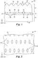
- Fig. 1 shows an illustrative optical film stack of the invention.
- Optical film stack 10 comprises light redirecting film assembly 12, light diffusion film assembly 14, and optical adhesive 16.
- Light redirecting film assembly 12 and light diffusion film assembly 14 are physically coupled, and collectively are unitary optical film stack 10.
- Light redirecting film assembly 12 comprises light redirecting film 18 and has first structured major surface 20 and opposing second major surface 22.
- Second major surface 22 has an array of protrusions 24 and land portions 26 surrounding protrusions 24.
- Light diffusion film assembly 14 has first major surface 28 and opposing second major surface 30.
- Second major surface 22 of light redirecting film assembly 12 is oriented toward first major surface 28 of light diffusion film assembly 14.
- Optical adhesive 16 is in a layer on first major surface 28. Protrusions 24 of light redirecting film assembly 12 extend into and adhere to the optical adhesive layer such that light redirecting film assembly 12 and light diffusion film assembly 14 are physically coupled into unitary optical film stack 10.
- light redirecting film assembly 12 and light diffusion film assembly 14 are coupled via protrusions 24 adhered to optical adhesive 16 with, corresponding to land portions 26, openings 32 in which an air interface is maintained to minimize the degree of optical coupling between physically coupled light redirecting film assembly 12 and light diffusion film assembly 14 in accordance with the invention.
- the functionality of the resultant optical film stack is determined in large part by the selection of constituent light redirecting film assembly 12, light diffusion film assembly 14, and optical adhesive 16.
- Light redirecting films used in optical stacks of the invention typically have a plurality of microstructures to impart desired light management properties to the optical film stack.
- the microstructures are an array of linear microprisms (e.g., such films often being referred to as "prismatic film") or other lenticular features.
- the microstructures are of selected geometry to impart desired light management properties to the optical film stack. Those skilled in the art will be able to readily select suitable light redirecting films, with appropriate configurations, to provide desired optical performance.
- the structured features may be any total-internal-reflection ("TIR") promoting replicated surface structures including prisms and/or lenticulars.
- TIR total-internal-reflection
- the surface structures can be continuous or piecewise continuous.
- the dimensions of the features may be uniform or irregular (e.g., have chaos variation). Though typically primarily linear structures are used, in-plane serpentine variations and/or variations in height along the peaks or from peak to peak of the linear structures may be imposed.
- the light redirecting film assembly comprises, and in some embodiments may consist essentially of, a light redirecting film.
- the light redirecting film assembly has a first major structure surface and an opposing second major structured surface.
- light redirecting film assembly 12 consists of light redirecting film 18.
- First major surface 20 of assembly 12 is made up of a plurality of microstructures 34 (e.g., linear prisms with peaks 36).
- Second major surface 22 of assembly 12 has protrusions 24.
- the light redirecting film assembly may be of monolayer or multilayer construction.
- An illustrative multilayer embodiment is shown in Fig. 3 , wherein light redirecting film assembly 312 has first major surface 320 and opposing second major surface 322.
- Assembly 312 comprises optic structured layer 333 with optically effective microstructures 334, body layer 335, and coupling protrusion layer 337 with protrusions 324.
- An advantage of multilayer embodiments is that the different layers may be separately optimized.
- relatively high refractive index materials e.g., in range of about 1.64 to about 1.7
- high gain resins polymeric materials of more conventional index of refraction (e.g., from about 1.48 to about 1.51) are well suited for use in the coupling protrusion layer.
- the light redirecting film assembly is manufactured from suitable optically effective materials.
- polymeric materials such as acrylic, polycarbonate, UV-cured acrylate, or the like, are used.
- the constituent layers are made of such materials, with different constituent layers in an assembly being made with the same or different materials.
- structured layer 333 may be made of cast and cured materials (e.g., ultraviolet-cured acrylics) cast on polyester body layer 335 (e.g., polyester terephthalate (“PET”)) as a substrate.
- PET polyester terephthalate
- Biaxially oriented PET is often preferred for its mechanical and optical properties.
- Physical coupling of the light redirecting film assembly to the light diffusion assembly to form the unitary optical stack of the invention is embodied in the protrusions projecting from the second major surface of the light redirecting assembly which penetrate into, and are bonded to, the adhesive on the first major surface of the light diffusion film.
- protrusions 24 project from second major surface 22 of light redirecting assembly 12. Protrusions 24 penetrate into, and are bonded to, adhesive 16 on first major surface 28 of the light diffusion film 14. In some embodiments, protrusions 24 may penetrate substantially completely through adhesive 16 and be in contact with first major surface 28 of light diffusion film assembly 14. In some embodiments, the protrusions may penetrate only partially through the adhesive.
- the protrusions are taller than the adhesive layer is thick. This facilitates manipulation of the component light redirecting film assembly and light diffusion assembly into desired position relative to one another including maintaining the air gaps critical to desired optical performance of the resultant optical film stack.
- the protrusions will be from about 4 to about 15 microns, typically preferably from about 8 to about 10 microns, tall. If the protrusions are too short, it may be more difficult to obtain the desired air gaps at the land portions of the second major surface of the light redirecting film assembly and the mechanical stability of the resultant optical film stack may be diminished. If the protrusions are too tall, the overall thickness of the resultant unitary optical film stack will tend to be greater. In some illustrative embodiments, the protrusions will be from about 8 to about 10 microns tall and the adhesive layer will be from about 5 to about 6 microns thick. If the adhesive layer is too thin, the mechanical stability of the resultant optical film stack will tend to be diminished.
- the adhesive layer is too thick, the overall thickness of the resultant unitary optical film stack will tend to be greater, and particularly if the protrusions are too short, it may be more difficult to obtain the desired air gaps at the land portions of the second major surface of the light redirecting film assembly.
- the protrusions in an optical film stack of the invention will typically be of substantially uniform size and shape. If desired, however, they may be made with variations in size, shape, or both if desired.
- the protrusions may be of any desired shape. They are preferably tapered from base or root 38 (where they project from the light redirecting film assembly) to the tip 40, as are protrusions 24 in Fig. 1 .
- the tip i.e., end of the protrusion opposite to the base
- the tip is typically preferably somewhat rounded (e.g., as are protrusions 24 in Fig. 1 ) to facilitate penetration into the adhesive layer, but may be flat (e.g., as are protrusions 524 in Fig. 5 ).
- the dimensions of the base of the protrusions may be of desired aspect ratio (i.e., relative dimensions in the x-y plane). Protrusions which are relatively smaller in base dimensions will tend to result in optical film stacks which exhibit relatively less optical coupling between the light redirecting film assembly and the light diffusion assembly but will also tend to exhibit relatively weaker physical integrity. Conversely, protrusions which are relatively larger in base dimensions will tend to result in optical film stacks which exhibit relatively more optical coupling between the light redirecting film assembly and the light diffusion assembly but will also tend to exhibit relatively stronger physical integrity.
- protrusions which are substantially V-shaped, with sides oriented at about 30° included angle and a tip which is curved to a radius of about 2 to about 3 microns are well suited for many applications with an effective combination of good physical coupling strength (and attendant robust physical characteristics of the optical film stack) and an acceptable level of optical coupling.
- Those skilled in the art will be able to optimize these parameters for particular applications in accordance with the invention.
- the protrusions have a longest base dimension of from about 4 to about 70 microns. Typically the longest base dimension is at least about 10 microns, typically preferably from about 40 to about 60 microns. In some embodiments, the protrusions have a shortest base dimension of from about 4 to about 12 microns. In some embodiments, the protrusions have a longest base dimension of from about 40 to about 60 microns and a shortest base dimension of from about 4 to about 12 microns. In some embodiments, the protrusions have a longest base dimension of from about 40 to about 60 microns, a shortest base dimension of from about 4 to about 12 microns, and a height of from about 4 to about 15 microns.
- the bases of the protrusions will constitute from about 10 to about 15% of the area of the second major surface of the light redirecting film assembly with remaining portion largely being land portions surrounding the protrusions.
- Embodiments with proportions outside this range may be made in accordance with the invention.
- embodiments in which the area proportion of protrusions is relatively lower will tend to exhibit relatively less optical coupling but will also tend to exhibit relatively weaker bonds, and therefore weaker physical integrity.
- embodiments in which the area proportion is relatively higher will tend to exhibit relatively stronger bonds, and therefore greater physical integrity, but will also tend to exhibit relatively more optical coupling.
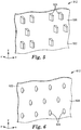
- the protrusions may be arranged in a uniform array (e.g., with uniform periodicity in x and y dimensions), or in a randomized array as desired.
- protrusions 524 are of uniform shape and size, but arranged in a random manner on second major surface 522 of light redirecting film assembly 512; whereas, in the embodiment shown in Fig. 6 , protrusions 624 are of uniform shape and size, and arranged in a uniform manner on second major surface 622 of light redirecting film assembly 612.
- the protrusions may be of any desired shape, for instance with a plurality of flat facets as protrusions 524 in Fig. 5 possess, or a single or plurality of rounded surfaces as the protrusions in Fig. 6 have. It has been observed that protrusions having rounder surfaces tend to yield optical film stacks exhibiting greater physical integrity as a result of greater surface area and stronger bonds than do protrusions with flat surfaces. Protrusions having relatively smaller tips tend to yield optical film stacks exhibiting lower levels of optical coupling than do protrusions having broader tips.
- Illustrative examples of shapes suitable for the protrusions include square, round, and oval pins, dune-like, linear, and intersecting shaped structures, etc.
- the cross sectional dimensions of the protrusions along the x and y axes may be relatively symmetrical or asymmetrical as desired.
- the protrusions have a cross sectional profile that is longer in one x or y dimension than at the other x or y dimension as such relatively elongate profiles tend to impart greater physical coupling integrity to the resultant optical film stack while minimizing the degree of optical coupling.
- the surface of the protrusions may be microstructured or roughened to increase the strength of the bond to the adhesive which is provided.
- protrusion 724a has flat side facets 723a and tip facet 725a while protrusion 724b has microstructured side facets 723b and tip facet 725b.
- an optical film stack comprising protrusions 724b would tend to exhibit greater physical integrity and lower optical coupling than would an optical film stack comprising smooth surfaced protrusions 724a.
- the facets of the protrusions may be flat, planar faces or curved. To facilitate fabrication and release from mold or embossing surfaces, it is typically preferred that the protrusions be tapered (i.e., with larger cross sectional dimension at the base that the tip), generally convex shapes, and have rounded tips.
- the light redirecting film assembly may be of unitary construction, having a first structured major surface optically effective microstructures thereon and an opposing second major surface from which the protrusions project.
- the assembly is made up of two or more component layers.
- Fig. 3 shows an embodiment wherein the assembly is made up of three component layers which may be laminated or self-adhered to one another, or which are attached using optical adhesive (not shown).
- the protrusions may be formed by many techniques, for instance, such as are used to form the optically effective microstructures.
- the protrusions can be fabricated by many techniques, illustrative examples including cast and cure, embossing, screen printing, deposition, flexo-printing, 3D printing or additive processing, etc., that yield a member having optically effective smooth land portions and the desired coupling structures.
- the protrusions do not need the fidelity of replication required of optically effective microstructures on the first major surface of the assembly.
- the light diffusion film assembly comprises light diffusion film. As shown in Fig. 4 , in a typical embodiment, light diffusion film assembly 414 comprises light diffusion film 413 having diffusing surface 415.
- the diffusing film is of beaded construction.
- the assembly may comprise a film having a layer of microscopic beads adhered to one surface of the film, and the refraction of light at the bead surfaces may operate to provide the light diffusion characteristics of the film.
- diffusing films use a structured surface other than a beaded layer to provide the light diffusion, where the structured surface is made by microreplication from a structured tool.
- diffusing films include: films (referred to herein as "Type I Microreplicated" diffusing films) with rounded or curved structures microreplicated from a tool having corresponding structures made by removing material from the tool with a cutter, as described in US Patent Appln. Publn. No. 2012/0113622 (Aronson et al. ), US Patent Appln. Publn. No. 2012/0147593 (Yapel et al. ), WO 2011/056475 (Barbie ), and WO 2012/0141261 (Aronson et al.
- microreplicated diffusing films include films in which a tool surface is made to be structured by a sandblasting procedure, and the structured surface is then imparted to the film by microreplication from the tool. See, for example, U.S. Patent 7,480,097 (Nagahama et al. ).
- the light diffusion film utilizes a surface refractive effect to achieve diffusion (e.g., such as structured surface type, and many beaded type diffusion films)
- a material with low index of refraction is coated over the light diffusing surface feature.
- the index of refraction of many optical adhesive materials is relatively close to the index of refraction of many surface refractive diffusing films, thus application of adhesive directly to the surface would greatly diminish or eliminate desired refractive index contrast (and thus diminish or eliminate desired diffusion).
- desired refraction-caused diffusion by light diffusion film 413 is achieved.
- Such an embodiment is shown in Fig. 4 , wherein low index layer 444 is provided on the surface refraction functional diffusion surface 415.
- refraction preservation layer 442 further comprises a skin layer or seal layer 446 over the surface of low index layer 444 opposite diffusion surface 415.
- seal layer 446 constitutes first major surface 428 of light diffusion film assembly 414. Absent such seal layer, the adhesive composition may penetrate into a porous low index layer, or degrade an incompatible low index layer, so as to degrade desired performance of the light diffusion assembly.
- such layers can be used to achieve a more planar first major surface 428, thereby facilitating effective adhesion of the optical adhesive to the first major surface of the light diffusion film assembly.
- Suitable materials for refractive preservation layer 442 may be readily selected.
- Illustrative examples of materials suitable for use as low index layer 444 in optical film stacks of the invention include low index optical films such as are disclosed in US Patent Appln. Publn. Nos. 2012/0038990 (Ho et al. ), 2012/0287677 (Wheatley et al. ), and 2016/0368019 (Wolk et al. ).
- US Patent Appln. Publn. No. 2015/(0140316 (Steiner et al. ) discloses a method for forming a low index material with protective coating which may be used in the present invention to form, with reference to Fig. 4 , a refraction preservation layer 442 comprising low index layer 444 with seal layer 446 (corresponding to, respectively, the "first layer” and "protective layer” of Steiner et al.).
- the adhesive preferably exhibits relatively low modulus and high flow properties during a "working phase" such that when contacted to the protrusions the adhesive will tend to wick up along at least a portion of, and encapsulate the surface of the protrusions without substantially wetting out the land portions of the coupling member between the protrusions. This leaves the desired air gap interface.
- the adhesive extends completely over the protrusion and contacts portions of the land adjacent the base of the protrusions, thereby forming relatively stronger bond.
- the combined cross sectional area of the protrusions and encapsulating adhesive will constitute from about 8 to about 25 percent, typically preferably about 10 to about 15 percent, of the total areal cross section (i.e., in x-y plane) of the optical film stack at the second major surface of the light redirecting film assembly, leaving a remaining about 92 to about 75 percent, typically about 90 to about 85 percent, of the total area as exposed land portions at which air gaps are provided in accordance with the invention.
- the physical coupling of the assemblies within the optical film stack is reduced, making the resultant stack more susceptible to fragmentation and failure, while at relatively higher proportions, although the physical coupling is stronger, optical coupling also tends to be higher.
- the adhesive After the adhesive achieves the desired flow and engagement with the protrusions, it is cured (e.g., by irradiation, etc.) to achieve a final secure bond and physical coupling of the light redirecting film assembly and light diffusion film assembly within the optical film stack.
- the adhesive After curing the adhesive achieves a high cross-linking density so as to function effectively as a structural adhesive, providing a strong bond.
- the invention thus provides a way to mechanically couple optical assemblies while minimizing resultant optical coupling.
- the invention enables the fabrication of component optical assemblies that offer many surprising advantages regarding easier handling, more physical robustness, reduced complexity and cost of devices in which they are incorporated, and high optical performance.
- Reference Number Feature 10 Unitary optical film stack 12
- Light redirecting film assembly 14 Light diffusion film assembly 16
- Optical adhesive 18 Light redirecting film 20
- Second major surface of light redirecting film assembly 24 Protrusions 25
- Protrusion tip 26 Land 28
- First major surface of light diffusion film assembly 30 Second major surface of light diffusion film assembly 32 Air gaps 34 Microstructures.
- BDF Beaded Diffusion Film
- Component Description Charge (lbs) %wt on dry solid SR9035 ethoxylated, trimethylolpropane triacrylate, from Sartomer 1.6 11.87 CAB-381-20 cellulose acetate butyrate, from Eastman Kodak 0.61 4.51 ESACURETM One difunctional alpha-hydroxy ketone, from Evonik Industries 0.1 0.76 TEGO® 2250 polyether-modified polysiloxane, from Evonik Industries 0.01 0.05 Dowanol® PM propylene glycol methylether, from Dow 13.57 0.0 MX 500 MX 500: 5 micron PMMA forming bodies, from Soken Chemical and Engineering Co.
- composition described above was applied on a primed sized 3 mil polyethylene terephthalate film via slide coating (as generally described in US Patent Nos. 6,214,111 and 6,576,296 except using select materials as described herein), heated and dried at 70°C, for 1.5 minutes, and then exposed to UV light for 1 to 2 seconds to yield the light diffusion film.
- a low index layer and seal layer which collectively constitute a refraction preservation layer were coated simultaneously onto the surface of the BDF using a multi-layer slide coating die.
- the bottom, or first layer (which formed the low index layer) was a 9% solids by weight (2% PYA solution) low index coating solution prepared by mixing 1.25 wt % Poval PVA 235, 37.5 wt % Cab-O-SperseTM PG-022, 0.07 wt % citric acid, 0.18 wt % boric acid, 0.025 wt % Tergitol Minfoam, 16 wt % isopropyl alcohol, and 44.975 wt % water.
- the second layer (which formed the seal layer) was a 4.2% solids by weight (4.2% PVA solution) protective layer prepared by mixing 4.14 wt % Poval PVA 235, 0.04 wt % citric acid, 0.025 wt % BYK 345, 25 wt % isopropyl alcohol, and 70.795 wt % water.
- the second layer was prepared so that it freely wet out the first layer on the slide coater.
- a slide coater was positioned at a gap of 0.008 inches from the BGD coating web moving at 100 ft/min (30.48 m/min).
- the first layer was pumped at 400 g/min to a slide coater having a first slot thickness of 0.008 inches (0.203 mm), a step height of 0.010 inches (0.254 mm) and a 13 in (33 cm) width
- the second layer was pumped at 180 g/min to the slide coater having a second slot thickness of 0.029 inches (0.737 mm), a step height of 0.020 inches (0.508 mm) and a 13 in (33 cm) width.
- the coated layers were then dried in a two zone oven.
- the first zone was 70 ft (21.3 meters) long and held at 75°C
- the second zone was also 70 ft (21.3 meters) long and held at 90°C, yielding a light diffusion film assembly with refraction preservation layer.
- the refractive index of low index layer was measured as 1.18, and the sealing layer was about 0.75 micron in thickness.
- Stock Solution I was prepared as follows: In a 1 gallon jar, 463.2 g of CN983, 193 g of CN3100, 386 g of EBECRYL® 230, 463 g of methyl ethyl ketone, 579 g of 1-methoxy-2-propanol were added. The mixture was put on a roller mixer for 6 hours to form a homogenous stock solution at 50% wt.
- Stock Solution II was prepared as follows: In a 1 gallon jar, 713 g of acrylate copolymer (60%wt solid in MEK) and 1524 g of MEK were added. The mixture was put on a roller for 6 hours to form a homogenous stock solution at 19.12% solid.
- Adhesive coating composition prepared as follows: In a glass jar, 559.5 g of Stock Solution II, 165 g of Stock Solution I, 247.5 g of 1-methoxy-2-propanol and 3.06 g of IRGACURE® 184 were mixed together to form a clear adhesive coating formulation with final content of 20% solids.
- the adhesive coating formulation was coated by a syringe-pump at various flow rates into a 20.8 cm (8-inch) wide slot-type coating die.
- the slot coating die uniformly distributed a 20.8 cm wide coating onto the first major surface of the light diffusion film assembly at a film speed of about 5ft/min (152 cm/min).
- the solvents were removed by transporting the assembly to a drying oven operating at 200°F for 2 minutes at a web speed of 5 ft/min.
- a thin brightness enhancement film with coupling structures on the opposite face from the prisms was laminated onto the adhesive coating through an on-line laminator, where the coupling projections were inserted into the adhesive coating.
- the laminated films was post-cured using a Fusion System Model I300P configured with an H-bulb (from Fusion UV Systems, Gaithersburg MD), operated at full power.
- the UV Fusion chamber was supplied with a flow of nitrogen that resulted in an oxygen concentration of approximately 50 ppm in the chamber.
- Coating thickness of the adhesive was controlled by adjusting the flow rate. Dry coating thickness for the three flow rates were 5.0 microns, 5.5 microns and 6.0 microns for flow rates of 5.7 cc/min, 6.29 cc/min and 6.86 cc/min, respectively.
- Comparative Example C1 was illustrative of the traditional two-film approach, in which a Thin Brightness Enhancement Film, or "TBEF" (3M Company, St. Paul, Minnesota) was simply positioned above a piece of the light diffusion film assembly prepared above with no adhesive whatsoever (i.e., they are mutually supported at their edges in a chassis or frame), leaving a natural air gap between the two optical films.
- Comparative Example C2 was illustrative of the use of an optically clear adhesive to bond the two optical film assemblies into a unitary stack with the adhesive forming a substantially continuous bond to each of the optical film assemblies.
- Example 1 illustrates the unitary film stack of the invention using protrusion structures to main sufficient air-gaps between light redirecting film and light diffusion film assemblies.
- the brightness gain was measured 1.776, significant higher than the results obtained from Comparative Example C2.
- Example 1 Samples of the optical stack of Example 1 were cut to 1 inch strips. The 1 inch strip samples were laminated on the carrier tape with the backside of light diffusion film assembly facing the tape. Then, the light redirecting film assembly was then separated from the optical film stack at a peel rate of 12 inch/min. The peel force was measured in the range of 170 to 230 g/in.
Landscapes
- Physics & Mathematics (AREA)
- Engineering & Computer Science (AREA)
- Health & Medical Sciences (AREA)
- Mechanical Engineering (AREA)
- Ophthalmology & Optometry (AREA)
- Manufacturing & Machinery (AREA)
- Nonlinear Science (AREA)
- Optics & Photonics (AREA)
- General Physics & Mathematics (AREA)
- Crystallography & Structural Chemistry (AREA)
- Chemical & Material Sciences (AREA)
- Mathematical Physics (AREA)
- Optical Elements Other Than Lenses (AREA)
- Laminated Bodies (AREA)
Applications Claiming Priority (2)
| Application Number | Priority Date | Filing Date | Title |
|---|---|---|---|
| US201662293689P | 2016-02-10 | 2016-02-10 | |
| PCT/US2017/017417 WO2017139611A1 (en) | 2016-02-10 | 2017-02-10 | Unitary optical film assembly |
Publications (3)
| Publication Number | Publication Date |
|---|---|
| EP3414621A1 EP3414621A1 (en) | 2018-12-19 |
| EP3414621A4 EP3414621A4 (en) | 2019-07-31 |
| EP3414621B1 true EP3414621B1 (en) | 2021-07-21 |
Family
ID=59563609
Family Applications (1)
| Application Number | Title | Priority Date | Filing Date |
|---|---|---|---|
| EP17750849.6A Active EP3414621B1 (en) | 2016-02-10 | 2017-02-10 | Unitary optical film assembly |
Country Status (7)
| Country | Link |
|---|---|
| US (1) | US11294106B2 (enExample) |
| EP (1) | EP3414621B1 (enExample) |
| JP (1) | JP2019511003A (enExample) |
| KR (1) | KR20180110022A (enExample) |
| CN (1) | CN108604024B (enExample) |
| TW (1) | TWI743084B (enExample) |
| WO (1) | WO2017139611A1 (enExample) |
Cited By (1)
| Publication number | Priority date | Publication date | Assignee | Title |
|---|---|---|---|---|
| EP4551387A1 (de) * | 2022-07-07 | 2025-05-14 | EcoCan GmbH | Verfahren zur herstellung einer strukturfolie, insbesondere lichtlenkfolie, und damit hergestellte lichtlenkfolie |
Families Citing this family (4)
| Publication number | Priority date | Publication date | Assignee | Title |
|---|---|---|---|---|
| KR20180036999A (ko) | 2015-08-05 | 2018-04-10 | 쓰리엠 이노베이티브 프로퍼티즈 컴파니 | 광학 확산 필름 라미네이트 및 제조 방법 |
| US20200341336A1 (en) * | 2018-01-08 | 2020-10-29 | 3M Innovative Properties Company | Optical film assemblies |
| WO2020128707A1 (en) * | 2018-12-18 | 2020-06-25 | 3M Innovative Properties Company | Polymeric film having structured surface |
| KR20230031651A (ko) * | 2021-08-27 | 2023-03-07 | 주식회사 루멘스 | 초슬림 백라이트 유닛 |
Family Cites Families (43)
| Publication number | Priority date | Publication date | Assignee | Title |
|---|---|---|---|---|
| US5396350A (en) * | 1993-11-05 | 1995-03-07 | Alliedsignal Inc. | Backlighting apparatus employing an array of microprisms |
| US20100302479A1 (en) | 1996-03-21 | 2010-12-02 | Aronson Joseph T | Optical article |
| US5780109A (en) | 1997-01-21 | 1998-07-14 | Minnesota Mining And Manufacturing Company | Die edge cleaning system |
| US6576296B1 (en) | 1998-03-10 | 2003-06-10 | 3M Innovative Properties Company | Web coating method and apparatus for continuous coating over splices |
| US7119873B2 (en) * | 2001-04-27 | 2006-10-10 | Fuji Photo Film Co., Ltd. | Polarizing plate and liquid crystal display using the same |
| US7624783B2 (en) * | 2006-07-12 | 2009-12-01 | Sensenig Luke G | Curtain system for domestic animal shelter |
| US7010212B2 (en) | 2002-05-28 | 2006-03-07 | 3M Innovative Properties Company | Multifunctional optical assembly |
| WO2004097466A1 (ja) * | 2003-04-28 | 2004-11-11 | Takiron Co. Ltd. | 電磁波シールド性光拡散シート |
| JP4238792B2 (ja) | 2004-08-04 | 2009-03-18 | ソニー株式会社 | 光拡散シート及びその製造方法、並びにスクリーン |
| US7339635B2 (en) | 2005-01-14 | 2008-03-04 | 3M Innovative Properties Company | Pre-stacked optical films with adhesive layer |
| JP2006337753A (ja) | 2005-06-02 | 2006-12-14 | Mitsubishi Rayon Co Ltd | 光拡散偏向シート及びその製造方法 |
| US20080049330A1 (en) * | 2006-08-25 | 2008-02-28 | 3M Innovative Properties Company | Light directing laminate |
| JP4320672B2 (ja) | 2006-12-06 | 2009-08-26 | ソニー株式会社 | 光学シートおよび表示装置 |
| JP5536977B2 (ja) * | 2007-03-30 | 2014-07-02 | パナソニック株式会社 | 面発光体 |
| JP2009015220A (ja) * | 2007-07-09 | 2009-01-22 | Toppan Printing Co Ltd | 光学シート及びそれを用いたバックライト・ユニット、ディスプレイ装置 |
| WO2009067576A1 (en) | 2007-11-21 | 2009-05-28 | 3M Innovative Properties Company | Optical films |
| US8248560B2 (en) | 2008-04-18 | 2012-08-21 | Pixtronix, Inc. | Light guides and backlight systems incorporating prismatic structures and light redirectors |
| JP2009294240A (ja) * | 2008-06-02 | 2009-12-17 | Toppan Printing Co Ltd | 光学シート、バックライトユニット、液晶表示装置及びディスプレイ装置 |
| WO2010075387A2 (en) | 2008-12-24 | 2010-07-01 | 3M Innovative Properties Company | Microsphere pressure sensitive adhesive composition |
| JP2010198735A (ja) * | 2009-02-20 | 2010-09-09 | Fujifilm Corp | 光学部材及び該光学部材を備えた有機エレクトロルミネッセンス表示装置 |
| TWI491930B (zh) | 2009-04-15 | 2015-07-11 | 3M新設資產公司 | 光學膜 |
| JP5823958B2 (ja) | 2009-06-02 | 2015-11-25 | スリーエム イノベイティブ プロパティズ カンパニー | 光再偏向フィルム及び該フィルムを使用したディスプレイ |
| KR20120061911A (ko) | 2009-08-25 | 2012-06-13 | 쓰리엠 이노베이티브 프로퍼티즈 컴파니 | 광 방향 전환 필름 및 이를 포함하는 디스플레이 시스템 |
| CN102483475B (zh) * | 2009-09-04 | 2014-05-21 | 住友化学株式会社 | 光扩散膜及其制造方法、光扩散性偏振板以及液晶显示装置 |
| JP5932652B2 (ja) | 2009-10-24 | 2016-06-08 | スリーエム イノベイティブ プロパティズ カンパニー | 光学構造物 |
| EP2493689A2 (en) | 2009-10-27 | 2012-09-05 | 3M Innovative Properties Company | Optical film with anti-warp surface |
| US8950924B2 (en) | 2009-12-08 | 2015-02-10 | 3M Innovative Properties Company | Optical constructions incorporating a light guide and low refractive index films |
| KR20120123741A (ko) | 2010-01-13 | 2012-11-09 | 쓰리엠 이노베이티브 프로퍼티즈 컴파니 | 미세 구조화 저 굴절률 나노공극형 층을 갖는 광학 필름 및 이의 제조 방법 |
| US8917447B2 (en) | 2010-01-13 | 2014-12-23 | 3M Innovative Properties Company | Microreplicated film for attachment to autostereoscopic display components |
| KR20110089721A (ko) | 2010-02-01 | 2011-08-09 | 경북대학교 산학협력단 | 유기 태양전지용 정공수송층 조성물, 이를 구비한 유기 태양전지, 및 이를 이용한 유기 태양전지 제조방법 |
| CN102834744B (zh) | 2010-04-12 | 2016-03-16 | 3M创新有限公司 | 光学叠堆 |
| KR20110125483A (ko) | 2010-05-13 | 2011-11-21 | 신화인터텍 주식회사 | 일체형 광학 시트 |
| TWI534458B (zh) | 2010-10-20 | 2016-05-21 | 3M新設資產公司 | 經保護之低折射率光學元件 |
| JP6247534B2 (ja) | 2010-10-20 | 2017-12-13 | スリーエム イノベイティブ プロパティズ カンパニー | 光学拡散性低屈折率要素 |
| CN103403073B (zh) | 2011-02-03 | 2015-10-14 | 3M创新有限公司 | 硬涂膜 |
| BR112014006707A2 (pt) | 2011-09-23 | 2017-03-28 | 3M Innovative Properties Co | artigos retrorrefletivos que incluem uma marca de segurança |
| WO2013096324A1 (en) * | 2011-12-21 | 2013-06-27 | 3M Innovative Properties Company | Optical film stack |
| WO2013148407A1 (en) | 2012-03-30 | 2013-10-03 | 3M Innovative Properties Company | Protective coating for low index material |
| WO2014081693A1 (en) | 2012-11-21 | 2014-05-30 | 3M Innovative Properties Company | Optical diffusing films and methods of making same |
| US9229141B2 (en) * | 2012-12-13 | 2016-01-05 | 3M Innovative Properties Company | Optical assembly |
| WO2015072420A1 (ja) * | 2013-11-13 | 2015-05-21 | シャープ株式会社 | 採光フィルム |
| JP5793590B2 (ja) * | 2014-02-15 | 2015-10-14 | 三菱樹脂株式会社 | 積層ポリエステルフィルム |
| KR20180036999A (ko) | 2015-08-05 | 2018-04-10 | 쓰리엠 이노베이티브 프로퍼티즈 컴파니 | 광학 확산 필름 라미네이트 및 제조 방법 |
-
2017
- 2017-02-10 JP JP2018541623A patent/JP2019511003A/ja active Pending
- 2017-02-10 KR KR1020187025423A patent/KR20180110022A/ko not_active Withdrawn
- 2017-02-10 US US16/076,004 patent/US11294106B2/en active Active
- 2017-02-10 WO PCT/US2017/017417 patent/WO2017139611A1/en not_active Ceased
- 2017-02-10 CN CN201780010928.XA patent/CN108604024B/zh not_active Expired - Fee Related
- 2017-02-10 EP EP17750849.6A patent/EP3414621B1/en active Active
- 2017-02-10 TW TW106104526A patent/TWI743084B/zh not_active IP Right Cessation
Non-Patent Citations (1)
| Title |
|---|
| None * |
Cited By (1)
| Publication number | Priority date | Publication date | Assignee | Title |
|---|---|---|---|---|
| EP4551387A1 (de) * | 2022-07-07 | 2025-05-14 | EcoCan GmbH | Verfahren zur herstellung einer strukturfolie, insbesondere lichtlenkfolie, und damit hergestellte lichtlenkfolie |
Also Published As
| Publication number | Publication date |
|---|---|
| EP3414621A4 (en) | 2019-07-31 |
| US11294106B2 (en) | 2022-04-05 |
| TW201741128A (zh) | 2017-12-01 |
| JP2019511003A (ja) | 2019-04-18 |
| EP3414621A1 (en) | 2018-12-19 |
| KR20180110022A (ko) | 2018-10-08 |
| TWI743084B (zh) | 2021-10-21 |
| CN108604024A (zh) | 2018-09-28 |
| CN108604024B (zh) | 2022-08-19 |
| US20210191003A1 (en) | 2021-06-24 |
| WO2017139611A1 (en) | 2017-08-17 |
Similar Documents
| Publication | Publication Date | Title |
|---|---|---|
| EP3414621B1 (en) | Unitary optical film assembly | |
| CN102596571B (zh) | 具有抗翘曲表面的光学膜 | |
| EP3894915B1 (en) | Liquid crystal display having a frontside light control film | |
| KR101154807B1 (ko) | 방현성 코팅 조성물, 방현 필름 및 그의 제조방법 | |
| CN103732390B (zh) | 带保护膜的微细凹凸结构体及其制造方法 | |
| KR101648280B1 (ko) | 적층체 | |
| KR20050004238A (ko) | 다기능 광학 조립체 | |
| JP2008176318A (ja) | 耐傷性薄膜 | |
| CN1924624A (zh) | 光学片用基质膜、光学片与背面照明装置 | |
| US20200132893A1 (en) | Optical assembly and the method to make the same | |
| WO2013140965A1 (ja) | 光学機能部材支持用複層フィルム、プリズムシート、光源ユニット及び表示装置 | |
| JP2004240087A (ja) | 積層偏光フィルム | |
| KR101271284B1 (ko) | 표시 화면용 기능 필름 및 그 제조법 | |
| US20190137080A1 (en) | Optical assembly and the method to make the same | |
| US10705266B2 (en) | Optical diffusing film laminate and method of making | |
| KR100676773B1 (ko) | 광확산 필름 | |
| KR100973599B1 (ko) | 보호필름이 제거된 광학필름 및 이의 제조방법 | |
| KR100947713B1 (ko) | 고휘도 광확산필름 | |
| JP2002148405A (ja) | 反射防止フィルムおよびそれを用いた低反射偏光板 | |
| CN114106389A (zh) | 光学薄膜、光学薄膜的制造方法、光学构件和图像显示装置 | |
| KR20170001026A (ko) | 편광판 및 이것이 구비된 액정표시장치 |
Legal Events
| Date | Code | Title | Description |
|---|---|---|---|
| STAA | Information on the status of an ep patent application or granted ep patent |
Free format text: STATUS: THE INTERNATIONAL PUBLICATION HAS BEEN MADE |
|
| PUAI | Public reference made under article 153(3) epc to a published international application that has entered the european phase |
Free format text: ORIGINAL CODE: 0009012 |
|
| STAA | Information on the status of an ep patent application or granted ep patent |
Free format text: STATUS: REQUEST FOR EXAMINATION WAS MADE |
|
| 17P | Request for examination filed |
Effective date: 20180807 |
|
| AK | Designated contracting states |
Kind code of ref document: A1 Designated state(s): AL AT BE BG CH CY CZ DE DK EE ES FI FR GB GR HR HU IE IS IT LI LT LU LV MC MK MT NL NO PL PT RO RS SE SI SK SM TR |
|
| AX | Request for extension of the european patent |
Extension state: BA ME |
|
| DAV | Request for validation of the european patent (deleted) | ||
| DAX | Request for extension of the european patent (deleted) | ||
| A4 | Supplementary search report drawn up and despatched |
Effective date: 20190627 |
|
| RIC1 | Information provided on ipc code assigned before grant |
Ipc: F21V 8/00 20060101ALI20190621BHEP Ipc: G02F 1/1335 20060101AFI20190621BHEP |
|
| STAA | Information on the status of an ep patent application or granted ep patent |
Free format text: STATUS: EXAMINATION IS IN PROGRESS |
|
| 17Q | First examination report despatched |
Effective date: 20200323 |
|
| GRAP | Despatch of communication of intention to grant a patent |
Free format text: ORIGINAL CODE: EPIDOSNIGR1 |
|
| STAA | Information on the status of an ep patent application or granted ep patent |
Free format text: STATUS: GRANT OF PATENT IS INTENDED |
|
| INTG | Intention to grant announced |
Effective date: 20210223 |
|
| GRAS | Grant fee paid |
Free format text: ORIGINAL CODE: EPIDOSNIGR3 |
|
| GRAA | (expected) grant |
Free format text: ORIGINAL CODE: 0009210 |
|
| STAA | Information on the status of an ep patent application or granted ep patent |
Free format text: STATUS: THE PATENT HAS BEEN GRANTED |
|
| AK | Designated contracting states |
Kind code of ref document: B1 Designated state(s): AL AT BE BG CH CY CZ DE DK EE ES FI FR GB GR HR HU IE IS IT LI LT LU LV MC MK MT NL NO PL PT RO RS SE SI SK SM TR |
|
| REG | Reference to a national code |
Ref country code: GB Ref legal event code: FG4D |
|
| REG | Reference to a national code |
Ref country code: CH Ref legal event code: EP |
|
| REG | Reference to a national code |
Ref country code: DE Ref legal event code: R096 Ref document number: 602017042506 Country of ref document: DE |
|
| REG | Reference to a national code |
Ref country code: AT Ref legal event code: REF Ref document number: 1413120 Country of ref document: AT Kind code of ref document: T Effective date: 20210815 |
|
| REG | Reference to a national code |
Ref country code: IE Ref legal event code: FG4D |
|
| REG | Reference to a national code |
Ref country code: LT Ref legal event code: MG9D |
|
| REG | Reference to a national code |
Ref country code: NL Ref legal event code: MP Effective date: 20210721 |
|
| REG | Reference to a national code |
Ref country code: AT Ref legal event code: MK05 Ref document number: 1413120 Country of ref document: AT Kind code of ref document: T Effective date: 20210721 |
|
| PG25 | Lapsed in a contracting state [announced via postgrant information from national office to epo] |
Ref country code: HR Free format text: LAPSE BECAUSE OF FAILURE TO SUBMIT A TRANSLATION OF THE DESCRIPTION OR TO PAY THE FEE WITHIN THE PRESCRIBED TIME-LIMIT Effective date: 20210721 Ref country code: RS Free format text: LAPSE BECAUSE OF FAILURE TO SUBMIT A TRANSLATION OF THE DESCRIPTION OR TO PAY THE FEE WITHIN THE PRESCRIBED TIME-LIMIT Effective date: 20210721 Ref country code: SE Free format text: LAPSE BECAUSE OF FAILURE TO SUBMIT A TRANSLATION OF THE DESCRIPTION OR TO PAY THE FEE WITHIN THE PRESCRIBED TIME-LIMIT Effective date: 20210721 Ref country code: LT Free format text: LAPSE BECAUSE OF FAILURE TO SUBMIT A TRANSLATION OF THE DESCRIPTION OR TO PAY THE FEE WITHIN THE PRESCRIBED TIME-LIMIT Effective date: 20210721 Ref country code: BG Free format text: LAPSE BECAUSE OF FAILURE TO SUBMIT A TRANSLATION OF THE DESCRIPTION OR TO PAY THE FEE WITHIN THE PRESCRIBED TIME-LIMIT Effective date: 20211021 Ref country code: AT Free format text: LAPSE BECAUSE OF FAILURE TO SUBMIT A TRANSLATION OF THE DESCRIPTION OR TO PAY THE FEE WITHIN THE PRESCRIBED TIME-LIMIT Effective date: 20210721 Ref country code: ES Free format text: LAPSE BECAUSE OF FAILURE TO SUBMIT A TRANSLATION OF THE DESCRIPTION OR TO PAY THE FEE WITHIN THE PRESCRIBED TIME-LIMIT Effective date: 20210721 Ref country code: FI Free format text: LAPSE BECAUSE OF FAILURE TO SUBMIT A TRANSLATION OF THE DESCRIPTION OR TO PAY THE FEE WITHIN THE PRESCRIBED TIME-LIMIT Effective date: 20210721 Ref country code: NO Free format text: LAPSE BECAUSE OF FAILURE TO SUBMIT A TRANSLATION OF THE DESCRIPTION OR TO PAY THE FEE WITHIN THE PRESCRIBED TIME-LIMIT Effective date: 20211021 Ref country code: NL Free format text: LAPSE BECAUSE OF FAILURE TO SUBMIT A TRANSLATION OF THE DESCRIPTION OR TO PAY THE FEE WITHIN THE PRESCRIBED TIME-LIMIT Effective date: 20210721 Ref country code: PT Free format text: LAPSE BECAUSE OF FAILURE TO SUBMIT A TRANSLATION OF THE DESCRIPTION OR TO PAY THE FEE WITHIN THE PRESCRIBED TIME-LIMIT Effective date: 20211122 |
|
| PG25 | Lapsed in a contracting state [announced via postgrant information from national office to epo] |
Ref country code: PL Free format text: LAPSE BECAUSE OF FAILURE TO SUBMIT A TRANSLATION OF THE DESCRIPTION OR TO PAY THE FEE WITHIN THE PRESCRIBED TIME-LIMIT Effective date: 20210721 Ref country code: LV Free format text: LAPSE BECAUSE OF FAILURE TO SUBMIT A TRANSLATION OF THE DESCRIPTION OR TO PAY THE FEE WITHIN THE PRESCRIBED TIME-LIMIT Effective date: 20210721 Ref country code: GR Free format text: LAPSE BECAUSE OF FAILURE TO SUBMIT A TRANSLATION OF THE DESCRIPTION OR TO PAY THE FEE WITHIN THE PRESCRIBED TIME-LIMIT Effective date: 20211022 |
|
| REG | Reference to a national code |
Ref country code: DE Ref legal event code: R097 Ref document number: 602017042506 Country of ref document: DE |
|
| PG25 | Lapsed in a contracting state [announced via postgrant information from national office to epo] |
Ref country code: DK Free format text: LAPSE BECAUSE OF FAILURE TO SUBMIT A TRANSLATION OF THE DESCRIPTION OR TO PAY THE FEE WITHIN THE PRESCRIBED TIME-LIMIT Effective date: 20210721 |
|
| PLBE | No opposition filed within time limit |
Free format text: ORIGINAL CODE: 0009261 |
|
| STAA | Information on the status of an ep patent application or granted ep patent |
Free format text: STATUS: NO OPPOSITION FILED WITHIN TIME LIMIT |
|
| PG25 | Lapsed in a contracting state [announced via postgrant information from national office to epo] |
Ref country code: SM Free format text: LAPSE BECAUSE OF FAILURE TO SUBMIT A TRANSLATION OF THE DESCRIPTION OR TO PAY THE FEE WITHIN THE PRESCRIBED TIME-LIMIT Effective date: 20210721 Ref country code: SK Free format text: LAPSE BECAUSE OF FAILURE TO SUBMIT A TRANSLATION OF THE DESCRIPTION OR TO PAY THE FEE WITHIN THE PRESCRIBED TIME-LIMIT Effective date: 20210721 Ref country code: RO Free format text: LAPSE BECAUSE OF FAILURE TO SUBMIT A TRANSLATION OF THE DESCRIPTION OR TO PAY THE FEE WITHIN THE PRESCRIBED TIME-LIMIT Effective date: 20210721 Ref country code: EE Free format text: LAPSE BECAUSE OF FAILURE TO SUBMIT A TRANSLATION OF THE DESCRIPTION OR TO PAY THE FEE WITHIN THE PRESCRIBED TIME-LIMIT Effective date: 20210721 Ref country code: CZ Free format text: LAPSE BECAUSE OF FAILURE TO SUBMIT A TRANSLATION OF THE DESCRIPTION OR TO PAY THE FEE WITHIN THE PRESCRIBED TIME-LIMIT Effective date: 20210721 Ref country code: AL Free format text: LAPSE BECAUSE OF FAILURE TO SUBMIT A TRANSLATION OF THE DESCRIPTION OR TO PAY THE FEE WITHIN THE PRESCRIBED TIME-LIMIT Effective date: 20210721 |
|
| 26N | No opposition filed |
Effective date: 20220422 |
|
| PG25 | Lapsed in a contracting state [announced via postgrant information from national office to epo] |
Ref country code: IT Free format text: LAPSE BECAUSE OF FAILURE TO SUBMIT A TRANSLATION OF THE DESCRIPTION OR TO PAY THE FEE WITHIN THE PRESCRIBED TIME-LIMIT Effective date: 20210721 |
|
| PG25 | Lapsed in a contracting state [announced via postgrant information from national office to epo] |
Ref country code: MC Free format text: LAPSE BECAUSE OF FAILURE TO SUBMIT A TRANSLATION OF THE DESCRIPTION OR TO PAY THE FEE WITHIN THE PRESCRIBED TIME-LIMIT Effective date: 20210721 |
|
| REG | Reference to a national code |
Ref country code: CH Ref legal event code: PL |
|
| REG | Reference to a national code |
Ref country code: BE Ref legal event code: MM Effective date: 20220228 |
|
| GBPC | Gb: european patent ceased through non-payment of renewal fee |
Effective date: 20220210 |
|
| PG25 | Lapsed in a contracting state [announced via postgrant information from national office to epo] |
Ref country code: LU Free format text: LAPSE BECAUSE OF NON-PAYMENT OF DUE FEES Effective date: 20220210 |
|
| PG25 | Lapsed in a contracting state [announced via postgrant information from national office to epo] |
Ref country code: FR Free format text: LAPSE BECAUSE OF NON-PAYMENT OF DUE FEES Effective date: 20220228 |
|
| PG25 | Lapsed in a contracting state [announced via postgrant information from national office to epo] |
Ref country code: LI Free format text: LAPSE BECAUSE OF NON-PAYMENT OF DUE FEES Effective date: 20220228 Ref country code: IE Free format text: LAPSE BECAUSE OF NON-PAYMENT OF DUE FEES Effective date: 20220210 Ref country code: GB Free format text: LAPSE BECAUSE OF NON-PAYMENT OF DUE FEES Effective date: 20220210 Ref country code: CH Free format text: LAPSE BECAUSE OF NON-PAYMENT OF DUE FEES Effective date: 20220228 |
|
| PG25 | Lapsed in a contracting state [announced via postgrant information from national office to epo] |
Ref country code: BE Free format text: LAPSE BECAUSE OF NON-PAYMENT OF DUE FEES Effective date: 20220228 |
|
| PGFP | Annual fee paid to national office [announced via postgrant information from national office to epo] |
Ref country code: DE Payment date: 20230119 Year of fee payment: 7 |
|
| P01 | Opt-out of the competence of the unified patent court (upc) registered |
Effective date: 20230530 |
|
| PG25 | Lapsed in a contracting state [announced via postgrant information from national office to epo] |
Ref country code: HU Free format text: LAPSE BECAUSE OF FAILURE TO SUBMIT A TRANSLATION OF THE DESCRIPTION OR TO PAY THE FEE WITHIN THE PRESCRIBED TIME-LIMIT; INVALID AB INITIO Effective date: 20170210 |
|
| PG25 | Lapsed in a contracting state [announced via postgrant information from national office to epo] |
Ref country code: MK Free format text: LAPSE BECAUSE OF FAILURE TO SUBMIT A TRANSLATION OF THE DESCRIPTION OR TO PAY THE FEE WITHIN THE PRESCRIBED TIME-LIMIT Effective date: 20210721 Ref country code: CY Free format text: LAPSE BECAUSE OF FAILURE TO SUBMIT A TRANSLATION OF THE DESCRIPTION OR TO PAY THE FEE WITHIN THE PRESCRIBED TIME-LIMIT Effective date: 20210721 |
|
| PG25 | Lapsed in a contracting state [announced via postgrant information from national office to epo] |
Ref country code: TR Free format text: LAPSE BECAUSE OF FAILURE TO SUBMIT A TRANSLATION OF THE DESCRIPTION OR TO PAY THE FEE WITHIN THE PRESCRIBED TIME-LIMIT Effective date: 20210721 |
|
| REG | Reference to a national code |
Ref country code: DE Ref legal event code: R119 Ref document number: 602017042506 Country of ref document: DE |
|
| PG25 | Lapsed in a contracting state [announced via postgrant information from national office to epo] |
Ref country code: MT Free format text: LAPSE BECAUSE OF FAILURE TO SUBMIT A TRANSLATION OF THE DESCRIPTION OR TO PAY THE FEE WITHIN THE PRESCRIBED TIME-LIMIT Effective date: 20210721 |
|
| PG25 | Lapsed in a contracting state [announced via postgrant information from national office to epo] |
Ref country code: DE Free format text: LAPSE BECAUSE OF NON-PAYMENT OF DUE FEES Effective date: 20240903 |
|
| PG25 | Lapsed in a contracting state [announced via postgrant information from national office to epo] |
Ref country code: DE Free format text: LAPSE BECAUSE OF NON-PAYMENT OF DUE FEES Effective date: 20240903 |