EP3411889B1 - Electromagnetic shielding for wireless power transfer systems - Google Patents
Electromagnetic shielding for wireless power transfer systems Download PDFInfo
- Publication number
- EP3411889B1 EP3411889B1 EP17777115.1A EP17777115A EP3411889B1 EP 3411889 B1 EP3411889 B1 EP 3411889B1 EP 17777115 A EP17777115 A EP 17777115A EP 3411889 B1 EP3411889 B1 EP 3411889B1
- Authority
- EP
- European Patent Office
- Prior art keywords
- shield
- transmitter
- receiver
- coil
- wireless charging
- Prior art date
- Legal status (The legal status is an assumption and is not a legal conclusion. Google has not performed a legal analysis and makes no representation as to the accuracy of the status listed.)
- Active
Links
Images





Classifications
-
- H—ELECTRICITY
- H01—ELECTRIC ELEMENTS
- H01F—MAGNETS; INDUCTANCES; TRANSFORMERS; SELECTION OF MATERIALS FOR THEIR MAGNETIC PROPERTIES
- H01F27/00—Details of transformers or inductances, in general
- H01F27/28—Coils; Windings; Conductive connections
- H01F27/2823—Wires
-
- H—ELECTRICITY
- H01—ELECTRIC ELEMENTS
- H01F—MAGNETS; INDUCTANCES; TRANSFORMERS; SELECTION OF MATERIALS FOR THEIR MAGNETIC PROPERTIES
- H01F27/00—Details of transformers or inductances, in general
- H01F27/34—Special means for preventing or reducing unwanted electric or magnetic effects, e.g. no-load losses, reactive currents, harmonics, oscillations, leakage fields
- H01F27/36—Electric or magnetic shields or screens
-
- H—ELECTRICITY
- H01—ELECTRIC ELEMENTS
- H01F—MAGNETS; INDUCTANCES; TRANSFORMERS; SELECTION OF MATERIALS FOR THEIR MAGNETIC PROPERTIES
- H01F27/00—Details of transformers or inductances, in general
- H01F27/34—Special means for preventing or reducing unwanted electric or magnetic effects, e.g. no-load losses, reactive currents, harmonics, oscillations, leakage fields
- H01F27/36—Electric or magnetic shields or screens
- H01F27/361—Electric or magnetic shields or screens made of combinations of electrically conductive material and ferromagnetic material
-
- H—ELECTRICITY
- H01—ELECTRIC ELEMENTS
- H01F—MAGNETS; INDUCTANCES; TRANSFORMERS; SELECTION OF MATERIALS FOR THEIR MAGNETIC PROPERTIES
- H01F38/00—Adaptations of transformers or inductances for specific applications or functions
- H01F38/14—Inductive couplings
-
- H—ELECTRICITY
- H02—GENERATION; CONVERSION OR DISTRIBUTION OF ELECTRIC POWER
- H02J—ELECTRIC POWER NETWORKS; CIRCUIT ARRANGEMENTS OR SYSTEMS FOR SUPPLYING OR DISTRIBUTING ELECTRIC POWER; SYSTEMS FOR STORING ELECTRIC ENERGY
- H02J50/00—Circuit arrangements or systems for wireless supply or distribution of electric power
- H02J50/10—Circuit arrangements or systems for wireless supply or distribution of electric power using inductive coupling
-
- H—ELECTRICITY
- H02—GENERATION; CONVERSION OR DISTRIBUTION OF ELECTRIC POWER
- H02J—ELECTRIC POWER NETWORKS; CIRCUIT ARRANGEMENTS OR SYSTEMS FOR SUPPLYING OR DISTRIBUTING ELECTRIC POWER; SYSTEMS FOR STORING ELECTRIC ENERGY
- H02J50/00—Circuit arrangements or systems for wireless supply or distribution of electric power
- H02J50/40—Circuit arrangements or systems for wireless supply or distribution of electric power using two or more transmitting or receiving devices
- H02J50/402—Circuit arrangements or systems for wireless supply or distribution of electric power using two or more transmitting or receiving devices the two or more transmitting or the two or more receiving devices being integrated in the same unit, e.g. power mats with several coils or antennas with several sub-antennas
-
- H—ELECTRICITY
- H02—GENERATION; CONVERSION OR DISTRIBUTION OF ELECTRIC POWER
- H02J—ELECTRIC POWER NETWORKS; CIRCUIT ARRANGEMENTS OR SYSTEMS FOR SUPPLYING OR DISTRIBUTING ELECTRIC POWER; SYSTEMS FOR STORING ELECTRIC ENERGY
- H02J50/00—Circuit arrangements or systems for wireless supply or distribution of electric power
- H02J50/70—Circuit arrangements or systems for wireless supply or distribution of electric power involving the reduction of electric, magnetic or electromagnetic leakage fields
Definitions
- Electronic devices operate when there is charge stored in their batteries.
- Some electronic devices include a rechargeable battery that can be recharged by coupling the electronic device to a power source through a physical connection, such as through a charging cord.
- a charging cord to charge a battery in an electronic device, however, requires the electronic device to be physically tethered to a power outlet.
- using a charging cord requires the mobile device to have a connector, typically a receptacle connector, configured to mate with a connector, typically a plug connector, of the charging cord.
- the receptacle connector typically includes a cavity in the electronic device that provides an avenue within which dust and moisture can intrude and damage the device.
- a user of the electronic device has to physically connect the charging cable to the receptacle connector in order to charge the battery.
- wireless charging devices have been developed to wirelessly charge electronic devices without the need for a charging cord.
- some electronic devices can be recharged by merely resting the device on a charging surface of a wireless charging device.
- a transmitter coil disposed below the charging surface may produce a time-varying magnetic flux that induces a current in a corresponding receiving coil in the electronic device.
- the induced current can be used by the electronic device to charge its internal battery.
- Some existing wireless charging devices and electronic devices configured for wireless charging have a number of disadvantages. For instance, some wireless charging devices generate an unintended voltage on a receiving coil. The unintended voltage can create noise in the electronic device within which the receiving coil is housed. The noise can cause disturbance of sensitive electronic components in the electronic device, such as touch-sensitive components like a touch-sensitive display. Additionally, the electronic devices also generate an unintended voltage on a transmitter coil in a wireless charging device. The unintended voltage can cause inefficiencies in wireless power transfer.
- Document WO 2014/178 645 A1 relates to a method for manufacturing a receiving antenna for a wireless charger and a receiving antenna for a wireless charger manufactured using the same.
- Document EP 3 364 433 A1 relates to an inductive module.
- Document EP 2 950 416 A2 relates to reducing the impact of an inductive energy transfer system on a touch sensing device.
- Document WO 2011/040 392 A1 relates to a device, a system, and a method for transmitting electric power and information.
- Document WO 2013/061 615 A1 relates to a contactless power transmission device, and a power supply device and power receiving device used therein.
- Document EP 2 814 046 A2 relates to a leakage preventing device of electromagnetic waves.
- WO 2011/040392 A1 and WO 2013/061615 A1 disclose that the device comprises an electromagnetic shield provided with diametrically opposed gaps.
- Some embodiments of the disclosure provide shielding components for a wireless charging system to avoid the generation of detrimental voltages on a receiver coil and/or a transmitter coil of a wireless charging system during wireless power transfer.
- a transmitter shield and a receiver shield are implemented in a wireless charging system to intercept electric fields generated between the transmitter coil and the receiver coil during wireless power transfer. By intercepting the electric fields, detrimental voltages are prevented from being generated on the receiver coil by the transmitter coil, and vice versa, during wireless power transfer.
- the invention provides wireless charging systems and electronic devices according to the independent claims. Further embodiments are provided in the dependent claims. The configurations disclosed in the following description which are not covered by the appended claims are useful for illustrating and understanding the invention.
- a wireless charging system according to the present invention is defined in independent claim 1.
- the transmitter shield and receiver shield can each be grounded to discharge voltage generated by the electric field.
- the transmitter shield can be positioned along the direction of the magnetic flux.
- the transmitter shield can be formed of a conductive material. In some embodiments, the conductive material can be NiV.
- the transmitter shield can have a thickness between 20-30 um.
- a wireless charging device configured to generate magnetic flux to perform wireless power transfer can include a driver board; a plurality of transmitter coils disposed above the driver board and configured to generate the magnetic flux upward; an electromagnetic shield disposed above the plurality of transmitter coils, and configured to be transparent to magnetic flux and opaque to electric fields, the electromagnetic shield including: a substrate comprising a stiff material; and a conductive layer disposed on a bottom surface of the substrate; and an adhesive layer disposed between the plurality of transmitter coils and the electromagnetic shield, the adhesive layer configured to attach the electromagnetic shield to the plurality of transmitter coils.
- the electromagnetic shield can further include conductive traces embedded within the conductive layer.
- the traces can be grounded.
- the traces can be positioned perpendicular to coils of wire of the plurality of transmitter coils.
- the conductive material can be NiV.
- the conductive material can have a thickness between 25 to 100 nm.
- the wireless charging device can further include a ferrite layer disposed between the driver board and the plurality of transmitter coils.
- the transmitter coil can include a coil of wire and an insulating material attached to the coil of wire.
- the insulating material can be PI.
- the electromagnetic shield can include a conductive layer.
- the conductive layer can be formed of silver.
- the electromagnetic shield can have a thickness between 0.05 and 0.15 ⁇ m.
- the conductive adhesive layer can be conductive pressure sensitive adhesive, CPSA.
- Transmitter coil 102 and receiver coil 104 can be positioned substantially concentric to one another to enable efficient power transfer by means of magnetic induction.
- transmitter coil 102 can generate time-varying magnetic flux 106, which can propagate through both device housings at interface 112 and be received by receiver coil 104.
- Time-varying magnetic flux 106 interacts with receiver coil 104 to generate a corresponding current in receiver coil 104.
- the generated current can be used to charge a battery for operating the electronic device.
- electric fields 108 and 110 can be unintentionally generated between transmitter and receiver coils 102 and 104 during wireless power transfer.
- transmitter coil 102 when transmitter coil 102 generates magnetic flux 106, a large voltage difference can exist between transmitter coil 102 and receive coil 104.
- the voltage on transmitter coil 102 in some cases can be larger than the voltage on receiver coil 104, thereby orienting some electric fields 108 toward receiver coil 104 and causing unintended voltage to be generated in receiver coil 104.
- voltage existing on receiver coil 104 may also orient some electric fields 110 toward transmitter coil 102 and cause detrimental voltage to be generated on transmitter coil 102.
- Detrimental voltages generated on receiver coil 104 may disturb and/or disrupt the operation of sensitive components disposed proximate to receiver coil 104, such as touch-sensitive devices like a touch-sensitive display. And, detrimental voltages generated on transmitter coil 102 may cause inefficiencies in power transfer.
- a wireless charging system that mitigates the unintentional generation of detrimental voltage on a receiver and/or a transmitter coil during wireless power transfer.
- One or more electromagnetic shielding components will be incorporated in the wireless charging system to prevent electric fields from generating detrimental voltages on the receiver and/or transmitter coils, while allowing time-varying magnetic flux to freely propagate between the transmitter and receiver coils to perform wireless power transfer.
- a transmitter shield can be implemented in a wireless charging device to prevent detrimental voltage from being generated on a receiver coil in an electronic device.
- the transmitter shield can be positioned in the wireless charging device to intercept electric fields generated by the transmitter coil to prevent the electric fields from exposing on the receiver coil. As a result, the intercepted electric fields may generate voltage on the transmitter shield instead of on the receiver coil. This voltage can then be discharged by routing the voltage to ground, thereby disposing of the detrimental voltage and preventing it from affecting sensitive electronic components in the electronic device.
- a receiver shield can also be implemented in the wireless charging system to prevent detrimental voltage from being generated on the transmitter coil in the wireless charging device.
- the receiver shield can also be positioned in the electronic device to intercept electric fields generated by the receiver coil so that the electric fields are not exposed to the transmitter coil. Voltage generated in die receiver shield can be discharged to ground to prevent detrimental voltage from being generated on the transmitter coil. Aspects and features of embodiments of such a wireless charging system are discussed in further detail herein.
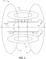
- transmitter shield 202 can be substantially transparent to magnetic flux 106
- transmitter shield 202 can, on the other hand, be substantially opaque to electric field 108 such that electric field 108 is substantially blocked by transmitter shield 202. This prevents electric field 108 from exposing on receiver coil 104 and generating an detrimental voltage on receiver coil 104. Because transmitter shield 202 substantially blocks electric field 108 before it can reach receiver coil 104, electric field 108 may generate voltage on transmitter shield 202 instead of receiver coil 104. The amount of voltage generated on transmitter shield 202 may correspond to the amount of voltage that would have been generated on transmitter coil 104 had transmitter shield 202 not been present.
- Voltage generated on transmitter shield 202 can be removed so that the voltage does not permanently remain on transmitter shield 202.
- voltage on transmitter shield 202 can be discharged to ground.
- transmitter shield 202 can be coupled to a ground connection 206 to allow voltage on transmitter shield 202 to be discharged to ground.
- Ground connection 206 can be a ground ring or any other suitable conductive structure coupled to ground that can remove voltage from transmitter shield 202.
- a receiver shield 204 may also be implemented in wireless charging system 200 to prevent detrimental voltage from being generated on transmitter coil 102 from electric field 110 generated by receiver coil 104.
- Receiver shield 204 may be positioned in front of receiver coil 104 so that magnetic flux 106 first passes through receiver shield 204 before exposing on receiver coil 104.
- Receiver shield 204 is positioned within a housing of an electronic device within which receiver coil 104 is also disposed. Thus, receiver shield 204 can be positioned between interface 112 and receiver coil 104 when the electronic device rests on a wireless charging device to perform wireless power transfer.
- transmitter and receiver shield 202 and 204 By incorporating transmitter and receiver shield 202 and 204 into wireless charging system 200, the wireless charging device and the electronic device within which transmitter and receiver shields 202 and 204 are implemented are exposing their grounds to each other. This mutes any ground noise caused by the electrical interactions between transmitter and receiver coils 102 and 104.
- transmitter shield 202 and receiver shield 204 are shielding structures that are able to block the passage of electric fields, yet allow the passage of magnetic flux. These shielding structures may include materials and thicknesses that are suitable for providing such electrical characteristics and functions. Details of the materials that can be used to form transmitter shields and receiver shields are discussed in further detail herein.
- An electromagnetic shield e.g., transmitter shield 202 and/or receiver shield 204, can be formed of a material having properties that enable magnetic flux to pass through but prevent electric fields from passing through.
- an electromagnetic shield can be formed of a non-conductive material. Non-conductive materials naturally allow magnetic flux to pass through but prevents electric fields from passing through.
- transmitter shield 202 can be formed of a conductive material that has a plurality of apertures. The conductive nature of the material allows voltage to be discharged to ground and the apertures provide avenues through which magnetic flux may tunnel to expose on transmitter shield 202.
- transmitter shield 202 can be formed of a very thin conductive material that allows magnetic flux to pass through but prevents electric fields from passing through. The thickness of the conductive material can be thin enough to allow passage of magnetic flux and have low enough resistance to allow voltage to travel through the conductive material in an efficient manner. Materials of various conductive properties and thicknesses are discussed in FIGS. 3 and 4 herein.
- FIG. 3 is a graph 300 representing a measure of mutual inductance achieved between a transmitter coil and a receiver coil when a shielding layer, e.g., any one of transmitter shield 202 or receiver shield 204, is disposed between the transmitter and receiver coils during wireless power transfer.
- the y-axis represents die percentage of mutual inductance attained between the transmitter and receiver coil increasing upward where 100% indicates that all of the magnetic flux generated by the transmitter coil is received by the receiver coil.
- the x-axis represents thickness of the shielding layer in a logarithmic scale ranging from 1.0E-05 to 1.0E-00 in millimeters increasing to the right.
- curves are plotted against graph 300 as shown in FIG. 3 .
- the various curves represent different conductive materials having different conductivities in terms of percentage of the conductivity of copper (i.e., % IACS, or percentage of the International Annealed Copper Standard).
- graph 300 may include curves representing materials having conductivities of 100% IACS, 10% IACS, 1% IACS, 0.1% IACS, 0.01% IACS, 0.001% IACS, and 0.001% IACS at a specific frequency of 10 MHz. Materials having higher conductivity, i.e., higher % IACS, means those materials are better at accommodating the movement of electric charge.
- each curve can provide guidance on selecting material of a certain conductivity and thickness to allow a high percentage of mutual inductance between the transmitter and receiver coil.
- each curve represents an achievable mutual inductance between the transmitter and receiver coils based on its thickness for different materials having different conductivities.
- a transmitter shield formed of a material having a conductivity of 100% IACS may allow a mutual inductance of 100% when its thickness is approximately 1.0E-05 mm.
- a transmitter shield formed of a material having a conductivity of 1% IACS may allow a mutual inductance of 100% when its thickness is less than approximately 1.0E-03.
- FIG. 4 is a graph 400 representing an alternating current resistance (ACR) of a material based on its thickness.
- the ACR of a material represents the amount of resistance a material has when an alternating current (AC) voltage is applied.
- the y-axis represents the amount of resistance of a material in units of ohms increasing upward, and the x-axis represents thickness of die shielding layer in a logarithmic scale in millimeters increasing to the right.
- the various curves may be curves for conductive materials having different conductivity in terms of % IACS. As shown in FIG. 4 , the curves represent materials having the same conductivities as those shown in graph 300 of FIG. 3 for ease of reference and cross comparison. The various curves can provide guidance on selecting material of a certain resistance and thickness to form a shield that can enable the efficient discharge of accumulated voltage from an electric field without generating excessive heat. In FIG. 4 , each curve may represent an amount of resistance based on its thickness for different materials having different conductivities.
- a transmitter shield formed of a material having a conductivity of 100% IACS may have a resistance of approximately 7 ohms when its thickness is approximately 1.0E-04 mm.
- a transmitter shield formed of a material having a conductivity of 1% IACS may have a resistance of approximately 10 ohms when its thickness is approximately 1.0E-02 mm.
- the ACR of a material can increase as thickness increases, but the ACR can be decreased by using materials with lower conductivity. Having higher resistance means that it is more difficult to discharge voltage accumulated on the shield. Moving voltage through a material having high resistance results in the dissipation of energy in the form of heat, which can decrease efficiency and cause damage to electrical components in excessive degrees.
- a transmitter shield and/or a receiver shield can be formed of a material that allows high mutual inductance of between 90-100% and a mutual ACR of less than 10 ohms with a desired thickness determined by device design constraints.
- an exemplary material that can be used to form a transmitter shield can include nickel vanadium (NiV) with a thickness ranging between 25 to 100 nm.
- the transmitter shield is formed of NiV with a thickness of approximately 50 nm.
- An preferred material that can be used to form a receiver shield can include silver with a thickness ranging between 0.05 and 0.15 ⁇ m.
- the receiver shield is formed of silver with a thickness of approximately 0.1 ⁇ m.
- the shields may be formed of a conductive material, other materials having similar properties can be used instead.
- a material including carbon may be used to form the electromagnetic shields.
- the transmitter shield may include carbon ink, such as N6X carbon ink.
- carbon ink can be easily customized to achieve the electrical properties desired to allow passage of magnetic flux while preventing passage of electric fields.
- carbon ink is represented by a vertical line. This is because the thickness of carbon ink is dictated by the process with which the carbon ink is deposited. For instance, typical printing processes can print carbon ink in thicknesses of approximately 25 ⁇ m.
- a transmitter shield can be included in a wireless charging device, such as a wireless charging mat
- a receiver shield can be included in an electronic device configured to rest on the wireless charging device to wirelessly receiver power from the wireless charging mat.
- FIG. 5 illustrates an exploded view of an exemplary wireless charging system 500 including a wireless charging device 502 and an electronic device 504, each having electromagnetic shielding.
- Wireless charging device 502 can generate time-varying magnetic flux to induce a corresponding current in electronic device 504 for performing wireless power transfer.
- Wireless charging mat 502 can include a housing formed of two shells: a first shell 505 and a second shell 506.
- First shell 505 can mate with second shell 506 to form an interior cavity within which internal components may be positioned.
- First and second shells 505 and 506 can also include notches 508a and 508b, respectively, that form an opening within the housing when first and second shells 505 and 506 are mated.
- An electrical connector 515 such as a receptacle connector, can be positioned within the opening so that wireless charging mat 500 can receive power from an external power source through a cable connected to electrical connector 515.
- the electrical connector 515 may include a plurality of contact pins and a plurality of terminals electrically coupled to the contact pins so that power can be routed from the external power source to the wireless charging mat 500 to provide power for wireless power transfer.
- the interior cavity formed between mated first and second shells 505 and 506 can include components that generate the magnetic flux for performing the wireless charging of electronic device 504.
- an array of transmitter coils 509 coupled to a driver board 510 can be housed within the inner cavity.
- Transmitter coils 509 can be operated to generate time-varying magnetic flux that propagate above the top surface of first shell 505 to induce a current in receiver coil 520 in electronic device 504.
- Driver board 510 can be a printed circuit board (PCB) configured to route signals and power for operating transmitter coils 509.
- PCB printed circuit board
- wireless charging device 502 includes a transmitter shield 512.
- Transmitter shield 512 is configured to allow passage of magnetic flux and to prevent passage of electric fields, as discussed herein with respect to transmitter shield 202 in FIG. 2 . Accordingly, transmitter shield 512 can be positioned within wireless charging device 502 in a suitable location for blocking electric field from exposing on a receiver coil 520 in electronic device 504. For example, transmitter shield 512 can be positioned in the direction of magnetic flux flow, such as between transmitter coils 509 and first shell 505.
- First shell 505 includes a charging surface 514 upon which electronic device 504 having receiver coil 520 may be placed to receive power from wireless charging mat 502.
- Charging surface 514 can be a generally planar region of a top surface of shell 505 where magnetic flux generated by transmitter coils 509 is present to induce a current in receiver coil 520 for charging an internal battery of electronic device 504.
- Electronic device 504 may merely rest on charging surface 512 to receive power from wireless charging device 502.
- the interface e.g., interface 112 in FIG. 1
- electronic device 504 makes contact with wireless charging device 502 can be a plane where respective housings of electronic device 504 and wireless charging device 502 make contact with each other.
- Magnetic flux generated by wireless charging device 502 can be shielded from internal components in electronic device 504 by a ferrite plate 522 Ferrite plate 522 is positioned above receiver coil 520 so that magnetic flux is first exposed to receiver coil 520 before being blocked by ferrite plate 522.
- Electronic device 504 can include atop housing 526 and a bottom housing 528 that can mate to form an inner cavity that houses internal components, such as receiver coil 520 and ferrite plate 522. Electronic device 504 can also include an electromagnetic shield within its inner cavity.
- electronic device 504 can include a receiver shield 524 that can be configured to allow magnetic flux generated by transmitter coils 509 to be received by receiver coil 520 but prevent electric fields from receiver coil 520 from exposing on transmitter coils 509, as discussed herein with respect to receiver shield 204 in FIG. 2 .
- Receiver shield 524 can be positioned within electronic device 504 in a suitable location for blocking electric field from exposing on transmitter coils 509 in wireless charging device 502. For example, receiver shield 524 can be positioned between receiver coils 520 and bottom housing 528. In this position, the magnetic flux first passes through receiver shield 524 before exposing on receiver coil 520.
- transmitter shield 512 and receiver shield 524 allows mutual inductance to exist between transmitter coils 509 and receiver coil 520, but prevents detrimental voltages from being generated in transmitter coils 509 and receiver coil 520. Preventing these voltages from being generated improves the operation of both wireless charging device 502 and electronic device by avoiding electrical disturbances.
- the transmitter shield and receiver shield can each be formed to have a specific structure suitable for implementation in a wireless charging system for performing wireless power transfer without generating detrimental voltages on the transmitter and receiver coils. Details of the structure of transmitter and receiver shields will be discussed further herein.
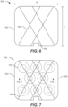
- FIG. 6 illustrates a top-down view of an exemplary transmitter shield 600.
- Transmitter shield 600 can be housed in a wireless charging device, such as a wireless charging mat, e.g., wireless charging mat 502 having transmitter shield 512 in FIG. 5 .
- Transmitter shield 600 can have dimensions that correspond to the dimensions of the wireless charging device.
- transmitter shield 600 can be in the shape of a rectangle having a width W and a length L that correspond to the width and length of the wireless charging device.
- transmitter shield 600 can be in the shape of a rectangle, it is to be appreciated that transmitter shields can have any other shape that corresponds to a wireless charging device, such as a square, rectangle, hexagon, triangle, and the like.
- a notch 606 may be formed at an edge of transmitter shield 600 to provide space for other components in a wireless charging mat, such as a receptacle connector for making connection with an external cable to receive power from an external source.
- Transmitter shield 600 may be coupled to ground at its edges 602 to discharge any voltage on transmitter shield 600. Voltage existing near the inner regions of transmitter shield 600 may have to travel to edges 602 by traversing across a large portion of transmitter shield 600, which may cause difficulties in routing the voltage to ground, e.g., by creating larger resistances. Thus, one or more conductive traces 604 may be embedded within transmitter shield 600 to assist with discharging voltage to ground. The low resistivity and high conductivity of traces 604 provides an avenue through which voltage can quickly travel to edges 602. Accordingly, transmitter shield 600 may be able to quickly discharge voltage to ground.
- Transmitter shield 600 can have dimensions that are suitable for shielding an array of transmitter coils disposed within the wireless charging device.
- FIG. 7 illustrates an exemplary wireless charging device 600 including transmitter shield 600 positioned over an array of transmitter coils 702.
- Transmitter coils 702 may be similar in function and form to transmitter coils 509 in FIG. 5 .
- Upper layers of wireless charging device 700 are not illustrated so that transmitter shield 600 and transmitter coils 702 can be seen.
- transmitter coils 702 are illustrated with dotted lines to indicate that transmitter coils are disposed below transmitter shield 600. Showing transmitter coils 702 helps to understand their relative position with respect to transmitter shield 600.
- transmitter shield 600 is large enough to cover the entire array of transmitter coils 708 so that each transmitter coil is shielded by transmitter shield 600.
- each transmitter coil 708 may generate magnetic flux that pass through transmitter shield 600 to induce a current on a receiver coil.
- Electric fields generated by the large voltage difference between a transmitter coil and a receiver coil may generate voltage in transmitter shield 600 around each transmitter coil. The generated voltage may flow across transmitter shield 600 to edges 602 and be discharged to ground.
- conductive traces 604 can be embedded in transmitter shield 600 to expedite the discharging of generated voltage on transmitter shield 600.
- Conductive trances 604 can be positioned over respective transmitter coils to route these voltages to ground at edges 602.
- conductive traces 604 can be positioned orthogonal to the windings of each transmitter coil 702 to minimize current generation in conductive traces 604 during operation of transmitter coils 702. This current can be generated by electrical interaction between conductive traces 604 and magnetic flux generated by transmitter coils 702. The induced current may impede the ability to discharge voltage on transmitter shield 600. Thus, arranging conductive traces 604 orthogonal to the winding of transmitter coils 702 may minimize this induced current.
- Transmitter shield 600 can be formed of a structure that includes more than one layer of material.
- FIG. 8 is a simplified diagram illustrating a cross section 800 of a transmitter shield and transmitter coils for a wireless charging device Specifically, FIG. 8 illustrates a cross-section of exemplary transmitter coil 702 and transmitter shield 600 shown in FIG. 6 .
- Transmitter shield 600 may be disposed above transmitter coils 702 so that magnetic flux generated by transmitter coils 702 may flow upward through transmitter shield 600 toward an interface surface 808.
- Interface surface 808 may be a top surface of a housing of the wireless charging device, such as charging surface 514 in FIG. 5 , that makes contact with a housing of an electrical device to perform wireless charging.
- Transmitter coils 702 can each be encapsulated by a protective layer such as coil encapsulating layer 810.
- Encapsulating layer 810 can be formed of any suitable non-conductive material for protecting transmitter coils 702, such as polyimide (PI).
- PI polyimide
- Transmitter shield 600 can include a conductive layer 802 for performing the electrical functions of transmitter shield 600.
- conductive layer 802 can be a layer of conductive material having properties that allow magnetic flux to pass through transmitter shield 600 but prevent electric fields from passing through transmitter shield 600, such as any of the conductive materials discussed herein with respect to FIGS. 3 and 4 .
- the conductive layer 802 can be formed of NiV having a thickness of approximately 50 nm.
- An adhesive layer 806 fixes conductive layer 802 over transmitter coils 702 so that conductive layer 802 is positioned to intercept electrical fields associated with transmitter coils 702 during wireless power transfer to prevent detrimental voltage from being generated on the receiver coil. Since transmitter coils 702 may not extend across the entire bottom surface of conductive layer 802, adhesive layer 806 may not have to extend across the entire bottom surface of conductive layer 802 either. Instead, adhesive layer 806 can just extend far enough to sufficiently couple transmitter coils 702 conductive layer 802. Adhesive layer 806 does not extend across the entire bottom surface of conductive layer 802, thereby reducing manufacturing cost. Adhesive layer 806 can be formed of any suitable non-conductive adhesive material. For example, adhesive layer 806 can be formed of pressure sensitive adhesive (PSA).
- PSA pressure sensitive adhesive
- FIG. 9 illustrates a top-down view of an exemplary receiver shield 900, according to embodiments of the present disclosure.
- Receiver shield 900 can be housed in an electronic device, such as a smart phone, smart watch, tablet, laptop, and the like, e.g., electronic device 504 having shield 524 in FIG. 5 .
- Receiver shield 900 can have dimensions that correspond to the dimensions of a receiver coil.
- receiver shield 900 can be generally circular in shape, or any other shape that corresponds to a receiver coil, such as a square, rectangle, hexagon, triangle, and the like.
- Receiver shield 900 has a gap 902 to provide an area where a connection to ground can be routed for discharging voltage generated on receiver shield 900. Additionally, gap 902 can provide space for other components of the electronic device, such as connection terminals for a receiver coil, as will be discussed further herein.
- connection to ground can be established at an end 904 of receiver shield 900 closest to the top of gap 902 so that voltage generated on receiver shield 900 can be discharged to ground. While providing a connection to ground at end 904 helps discharge voltage on receiver shield 900, The performance of receiver shield 900 is improved by including a cut 908 in receiver shield 900 positioned opposite of gap 902 to electrically separate receiver shield 900 into two halves: first half 910 and second half 912. A connection to ground can be provided at end 906 closes to the bottom of gap 902 so that both halves 910 and 912 can be coupled to ground to discharge any voltage generated in receiver shield 900.
- the potential difference between ends 904 and 906 may be based on the voltage captured by the entire surface area of receiver shield 900. This can cause a large potential difference to build up between ends 904 and 906, and can be difficult to discharge to ground. By including cut 908, the potential difference can be substantially decreased, such as by a half, thereby making it easier to discharge the voltage to ground.
- Receiver shield 900 can have dimensions that are suitable for shielding a receiver coil disposed within the electronic device.
- FIG. 10 illustrates a top-down view of an exemplary receiver system 1000 for an electronic device.
- Receiver system 1000 can include receiver shield 900, a ferrite plate 1002, and a receiver coil 1004 positioned between receiver shield 900 and ferrite plate 1002.
- Receiver coil 1004 is illustrated with dotted lines to indicate that transmitter coils are disposed behind receiver shield 900 as shown from the top-down perspective of FIG. 10 . Showing receiver coil 1004 helps to understand its relative position with respect to receiver shield 900.
- receiver shield 900 is large enough to cover the entire receiver coil 1004 so that receiver coil 900 is completely shielded by receiver shield 900.
- Receiver coil 1004 can have a flat, disc-like shape formed of a winding of coil that is wound from an inner diameter to an outer diameter.
- receiver shield 900 can also have a disk-like shape that has a corresponding inner and outer diameter.
- an electric field from receiver coil 900 can generate a voltage in receiver shield 900. The generated voltage may flow across receiver shield 900 to at least one of ends 904 and 906 and be discharged to ground.
- Connection terminals 1006 can be positioned in gap 902 of receiver shield 900. Connection terminals 1006 can provide electrical routes through which current induced in receiver coil 1004 can be routed to provide power to charge a battery in the electronic device. Additionally, connection terminals 1006 can include ground lines for routing voltage in receiver shield 900 to ground. For instance, receiver shield 900 can include a single ground line for routing voltage from the entire receiver shield 900 to ground (e.g., in instances where cut 908 is not present), or it can include two ground lines, one for routing voltage from first half 910 of receiver shield 900 to ground, and another for routing voltage from a second half 912 of receiver shield 900 to ground. Each ground line can be positioned close to the respective end for which it discharges voltage to ground. For example, the ground line for grounding first half 910 can be positioned close to end 904, while the ground line for grounding second half 912 can be positioned close to end 906.
- Ferrite plate 1002 can be positioned on a side of receiver coil 1004 opposite of the side on which receiver shield 900 is positioned. Ferrite plate 1002 can prevent magnetic flux and electrical fields from disturbing sensitive electrical components within the electronic device. Ferrite plate 1002 can be formed of any suitable ferromagnetic material. To better understand the structural layering of receiver system 1000, a cross-sectional view of receiver system 1000 is shown in FIG. 11 .
- FIG. 11 is a simplified diagram illustrating a cross section 1100 of receiver system 1000.
- Receiver system 1000 can include receiver shield 900 coupled to receiver coil 1004, which is coupled to ferrite plate 1002.
- Receiver coil 1004 can be positioned below ferrite plate 1002 so that ferrite plate 1002 can protect sensitive electrical components from magnetic flux and electrical fields generated during wireless power transfer.
- Receiver shield 900 may be disposed below receiver coil 1004 so that magnetic flux generated by a transmitter may flow upward from interface surface 1108 through receiver shield 900 before being received by receiver coil 1004.
- Interface surface 1108 may be a bottom surface of a housing of the electronic device that makes contact with a charging surface of a wireless charging device for performing wireless charging.
- Receiver coil 1004 can be encapsulated by a protective layer, such as coil encapsulating layer 1110.
- Encapsulating layer 1110 can be formed of any suitable non-conductive material for protecting receiver coil 1004, such as polyimide (PI).
- PI polyimide
- Receiver shield 900 can be formed of a layer of conductive material that can perform the electrical functions of a receiver shield discussed herein.
- receiver shield 900 can be a layer of conductive material having properties that allow magnetic flux to pass through receiver shield 900 but prevent electric fields from passing through receiver shield 900, such as any of the conductive materials discussed herein with respect to FIGS. 3 and 4 .
- Receiver shield 900 can be formed of silver, such as silver flake, having a thickness of approximately 0.1 ⁇ m.
- Receiver shield 900 is coupled to receiver coil 1004 by an adhesive layer 1102.
- Adhesive layer 1102 may fix receiver shield 900 underneath receiver coil 900 so that receiver shield 900 is positioned to intercept electrical fields associated with receiver shield 900 during wireless power transfer to prevent detrimental voltage from being generated on the transmitter coil.
- Adhesive layer 1102 can be configured to route voltage to ground by coupling with a connection terminal, such as connection terminal 1006 in FIG. 10 .
- adhesive layer 1102 is formed of any suitable conductive adhesive material.
- adhesive layer 1102 can be formed of conductive pressure sensitive adhesive (CPSA).
- Receiver shield 900 can be covered by a protective layer 1104.
- Protective layer 1104 can be positioned below receiver shield 900 to cover any exposed surfaces and prevent receiver shield 900 from oxidizing.
- Protective layer can be formed of any suitable dielectric material.
Landscapes
- Engineering & Computer Science (AREA)
- Power Engineering (AREA)
- Computer Networks & Wireless Communication (AREA)
- Physics & Mathematics (AREA)
- Electromagnetism (AREA)
- Charge And Discharge Circuits For Batteries Or The Like (AREA)
- Shielding Devices Or Components To Electric Or Magnetic Fields (AREA)
- Regulation Of General Use Transformers (AREA)
Description
- This application claims the benefit to
U.S. Non-Provisional Patent Application No. 15/701,224 filed September 11, 2017 U.S. Non-Provisional Patent Application No. 15/701,237 filed September 11, 2017 U.S. Provisional Patent Application No. 62/399,082 filed September 23, 2016 U.S. Provisional Patent Application No. 62/542,210 filed August 7, 2017 U.S. Provisional Patent Application No. 62/459,149 filed February 15, 2017 U.S. Provisional Patent Application No. 62/542,206 filed August 7, 2017 - Electronic devices (e.g., mobile phones, media players, electronic watches, and the like) operate when there is charge stored in their batteries. Some electronic devices include a rechargeable battery that can be recharged by coupling the electronic device to a power source through a physical connection, such as through a charging cord. Using a charging cord to charge a battery in an electronic device, however, requires the electronic device to be physically tethered to a power outlet. Additionally, using a charging cord requires the mobile device to have a connector, typically a receptacle connector, configured to mate with a connector, typically a plug connector, of the charging cord. The receptacle connector typically includes a cavity in the electronic device that provides an avenue within which dust and moisture can intrude and damage the device. Furthermore, a user of the electronic device has to physically connect the charging cable to the receptacle connector in order to charge the battery.
- To avoid such shortcomings, wireless charging devices have been developed to wirelessly charge electronic devices without the need for a charging cord. For example, some electronic devices can be recharged by merely resting the device on a charging surface of a wireless charging device. A transmitter coil disposed below the charging surface may produce a time-varying magnetic flux that induces a current in a corresponding receiving coil in the electronic device. The induced current can be used by the electronic device to charge its internal battery.
- Some existing wireless charging devices and electronic devices configured for wireless charging have a number of disadvantages. For instance, some wireless charging devices generate an unintended voltage on a receiving coil. The unintended voltage can create noise in the electronic device within which the receiving coil is housed. The noise can cause disturbance of sensitive electronic components in the electronic device, such as touch-sensitive components like a touch-sensitive display. Additionally, the electronic devices also generate an unintended voltage on a transmitter coil in a wireless charging device. The unintended voltage can cause inefficiencies in wireless power transfer.
- Document
WO 2014/178 645 A1 relates to a method for manufacturing a receiving antenna for a wireless charger and a receiving antenna for a wireless charger manufactured using the same. -
Document EP 3 364 433 A1 relates to an inductive module. - Document
US 2013/0 181535 A1 relates to wireless power transfer. - Document
EP 2 950 416 A2 relates to reducing the impact of an inductive energy transfer system on a touch sensing device. - Document
WO 2011/040 392 A1 relates to a device, a system, and a method for transmitting electric power and information. - Document
WO 2013/061 615 A1 relates to a contactless power transmission device, and a power supply device and power receiving device used therein. - Document
EP 2 814 046 A2 relates to a leakage preventing device of electromagnetic waves. - Especially,
WO 2011/040392 A1 andWO 2013/061615 A1 disclose that the device comprises an electromagnetic shield provided with diametrically opposed gaps. - Some embodiments of the disclosure provide shielding components for a wireless charging system to avoid the generation of detrimental voltages on a receiver coil and/or a transmitter coil of a wireless charging system during wireless power transfer. In some aspects, a transmitter shield and a receiver shield are implemented in a wireless charging system to intercept electric fields generated between the transmitter coil and the receiver coil during wireless power transfer. By intercepting the electric fields, detrimental voltages are prevented from being generated on the receiver coil by the transmitter coil, and vice versa, during wireless power transfer.
- The invention provides wireless charging systems and electronic devices according to the independent claims. Further embodiments are provided in the dependent claims. The configurations disclosed in the following description which are not covered by the appended claims are useful for illustrating and understanding the invention.
- A wireless charging system according to the present invention is defined in
independent claim 1. - The transmitter shield and receiver shield can each be grounded to discharge voltage generated by the electric field. The transmitter shield can be positioned along the direction of the magnetic flux. The transmitter shield can be formed of a conductive material. In some embodiments, the conductive material can be NiV. The transmitter shield can have a thickness between 20-30 um.
- A wireless charging device configured to generate magnetic flux to perform wireless power transfer can include a driver board; a plurality of transmitter coils disposed above the driver board and configured to generate the magnetic flux upward; an electromagnetic shield disposed above the plurality of transmitter coils, and configured to be transparent to magnetic flux and opaque to electric fields, the electromagnetic shield including: a substrate comprising a stiff material; and a conductive layer disposed on a bottom surface of the substrate; and an adhesive layer disposed between the plurality of transmitter coils and the electromagnetic shield, the adhesive layer configured to attach the electromagnetic shield to the plurality of transmitter coils.
- The electromagnetic shield can further include conductive traces embedded within the conductive layer. The traces can be grounded. The traces can be positioned perpendicular to coils of wire of the plurality of transmitter coils. The conductive material can be NiV. The conductive material can have a thickness between 25 to 100 nm. The wireless charging device can further include a ferrite layer disposed between the driver board and the plurality of transmitter coils.
- Additionally, a electronic device according to the present invention is defined in independent claim 11.
- The transmitter coil can include a coil of wire and an insulating material attached to the coil of wire. The insulating material can be PI. The electromagnetic shield can include a conductive layer. The conductive layer can be formed of silver. The electromagnetic shield can have a thickness between 0.05 and 0.15 µm. The conductive adhesive layer can be conductive pressure sensitive adhesive, CPSA.
- A better understanding of the nature and advantages of embodiments of the present invention as defined in the dependent claims, may be gained with reference to die following detailed description and die accompanying drawings.
-
-
FIG. 1 is a simplified diagram illustrating electrical interactions between a transmitter coil and a receiver coil of a wireless charging system during wireless power transfer. -
FIG. 2 is a simplified diagram illustrating an exemplary wireless charging system including a transmitter shield and a receiver shield. -
FIG. 3 is a graph representing a measure of mutual inductance achieved between a transmitter coil and a receiver coil when a shielding layer is disposed between the transmitter and receiver coils during wireless power transfer, according to some embodiments of the present disclosure. -
FIG. 4 is a graph representing an alternating current resistance (ACR) of a material based on its thickness. -
FIG. 5 illustrates an exploded view of an exemplary wireless charging system including a wireless charging device and an electronic device, each having electromagnetic shielding. -
FIG. 6 illustrates a top-down view of an exemplary transmitter shield. -
FIG. 7 illustrates a transmitter shield positioned over an array of transmitter coils. -
FIG. 8 illustrates a cross-section of a transmitter shield positioned over an array of transmitter coils. -
FIG. 9 illustrates a top-down view of a receiver shield. -
FIG. 10 illustrates a receiver shield positioned over a receiver coil. -
FIG. 11 illustrates a cross-section of a receiver shield positioned over a receiver coil. - During wireless power transfer in a wireless charging system, numerous electrical interactions can occur between a transmitter coil and a receiver coil in the wireless charging system. Some of the electrical interactions are intended interactions between the transmitter and receiver coil, while other electrical interactions are unintended interactions that can cause inefficiencies in power transfer and create issues in the electronic device. For example,
FIG. 1 is a simplified diagram illustrating electrical interactions between atransmitter coil 102 and areceiver coil 104 of an exemplarywireless charging system 100 during wireless power transfer.Transmitter coil 102 may be disposed within a wireless charging device, such as a wireless charging mat, andreceiver coil 104 may be disposed within a consumer electronic device, such as a smart phone, smart watch, tablet, laptop, and the like. The electronic device may rest on the wireless charging device atinterface 112 to enable power transfer. -
Transmitter coil 102 andreceiver coil 104 can be positioned substantially concentric to one another to enable efficient power transfer by means of magnetic induction. During wireless power transfer,transmitter coil 102 can generate time-varyingmagnetic flux 106, which can propagate through both device housings atinterface 112 and be received byreceiver coil 104. Time-varyingmagnetic flux 106 interacts withreceiver coil 104 to generate a corresponding current inreceiver coil 104. The generated current can be used to charge a battery for operating the electronic device. - In addition to time-varying
magnetic flux 106, however,electric fields receiver coils transmitter coil 102 generatesmagnetic flux 106, a large voltage difference can exist betweentransmitter coil 102 and receivecoil 104. The voltage ontransmitter coil 102 in some cases can be larger than the voltage onreceiver coil 104, thereby orienting someelectric fields 108 towardreceiver coil 104 and causing unintended voltage to be generated inreceiver coil 104. In some additional cases, voltage existing onreceiver coil 104 may also orient someelectric fields 110 towardtransmitter coil 102 and cause detrimental voltage to be generated ontransmitter coil 102. Detrimental voltages generated onreceiver coil 104 may disturb and/or disrupt the operation of sensitive components disposed proximate toreceiver coil 104, such as touch-sensitive devices like a touch-sensitive display. And, detrimental voltages generated ontransmitter coil 102 may cause inefficiencies in power transfer. - Disclosed herein is a wireless charging system that mitigates the unintentional generation of detrimental voltage on a receiver and/or a transmitter coil during wireless power transfer. One or more electromagnetic shielding components will be incorporated in the wireless charging system to prevent electric fields from generating detrimental voltages on the receiver and/or transmitter coils, while allowing time-varying magnetic flux to freely propagate between the transmitter and receiver coils to perform wireless power transfer.
- A transmitter shield can be implemented in a wireless charging device to prevent detrimental voltage from being generated on a receiver coil in an electronic device. The transmitter shield can be positioned in the wireless charging device to intercept electric fields generated by the transmitter coil to prevent the electric fields from exposing on the receiver coil. As a result, the intercepted electric fields may generate voltage on the transmitter shield instead of on the receiver coil. This voltage can then be discharged by routing the voltage to ground, thereby disposing of the detrimental voltage and preventing it from affecting sensitive electronic components in the electronic device. In addition to the transmitter shield, a receiver shield can also be implemented in the wireless charging system to prevent detrimental voltage from being generated on the transmitter coil in the wireless charging device. Similar to the transmitter shield, the receiver shield can also be positioned in the electronic device to intercept electric fields generated by the receiver coil so that the electric fields are not exposed to the transmitter coil. Voltage generated in die receiver shield can be discharged to ground to prevent detrimental voltage from being generated on the transmitter coil. Aspects and features of embodiments of such a wireless charging system are discussed in further detail herein.
-
FIG. 2 is a simplified diagram illustrating an exemplarywireless charging system 200 including atransmitter shield 202 and areceiver shield 204.Transmitter shield 202 may be positioned in front oftransmitter coil 102 so thatmagnetic flux 106 is directed towardtransmitter shield 202. For instance,transmitter shield 202 is positioned betweentransmitter coil 102 andreceiver coil 104 during wireless power transfer so thatmagnetic flux 106 first passes throughtransmitter shield 202 before reachingreceiver coil 104.Transmitter shield 202 can be positioned betweeninterface 112 andtransmitter coil 102 when an electronic device rests on the wireless charging device to perform wireless power transfer. Accordingly,transmitter shield 202 andtransmitter coil 102 can both be positioned within the wireless charging device.Transmitter shield 202 can be substantially transparent tomagnetic flux 106 so that a substantial percentage ofmagnetic flux 106 generated bytransmitter coil 102 is received byreceiver 104. - While
transmitter shield 202 can be substantially transparent tomagnetic flux 106,transmitter shield 202 can, on the other hand, be substantially opaque toelectric field 108 such thatelectric field 108 is substantially blocked bytransmitter shield 202. This preventselectric field 108 from exposing onreceiver coil 104 and generating an detrimental voltage onreceiver coil 104. Becausetransmitter shield 202 substantially blockselectric field 108 before it can reachreceiver coil 104,electric field 108 may generate voltage ontransmitter shield 202 instead ofreceiver coil 104. The amount of voltage generated ontransmitter shield 202 may correspond to the amount of voltage that would have been generated ontransmitter coil 104 hadtransmitter shield 202 not been present. - Voltage generated on
transmitter shield 202 can be removed so that the voltage does not permanently remain ontransmitter shield 202. As an example, voltage ontransmitter shield 202 can be discharged to ground. Thus,transmitter shield 202 can be coupled to aground connection 206 to allow voltage ontransmitter shield 202 to be discharged to ground.Ground connection 206 can be a ground ring or any other suitable conductive structure coupled to ground that can remove voltage fromtransmitter shield 202. - Similar to
transmitter shield 202, areceiver shield 204 may also be implemented inwireless charging system 200 to prevent detrimental voltage from being generated ontransmitter coil 102 fromelectric field 110 generated byreceiver coil 104.Receiver shield 204 may be positioned in front ofreceiver coil 104 so thatmagnetic flux 106 first passes throughreceiver shield 204 before exposing onreceiver coil 104.Receiver shield 204 is positioned within a housing of an electronic device within whichreceiver coil 104 is also disposed. Thus,receiver shield 204 can be positioned betweeninterface 112 andreceiver coil 104 when the electronic device rests on a wireless charging device to perform wireless power transfer. - Similar to
transmitter shield 202,receiver shield 204 can be substantially transparent tomagnetic flux 106 so that a substantial percentage ofmagnetic flux 106 generated bytransmitter coil 102 passes throughreceiver shield 204 and is received byreceiver 104, whilereceiver shield 204 can be substantially opaque toelectric field 110 such thatelectric field 110 is substantially blocked byreceiver shield 204. This preventselectric field 110 from being exposed totransmitter coil 102 and generating an detrimental voltage ontransmitter coil 102 while enabling wireless power transfer. Liketransmitter shield 202,receiver shield 204 may also be grounded so that voltage generated byelectric field 110 may be discharged to aground connection 208.Ground connection 208 may be a structure similar toground connection 206, or it may be the same structure asground connection 206. - By incorporating transmitter and
receiver shield wireless charging system 200, the wireless charging device and the electronic device within which transmitter andreceiver shields receiver coils - As can be appreciated by disclosures herein,
transmitter shield 202 andreceiver shield 204 are shielding structures that are able to block the passage of electric fields, yet allow the passage of magnetic flux. These shielding structures may include materials and thicknesses that are suitable for providing such electrical characteristics and functions. Details of the materials that can be used to form transmitter shields and receiver shields are discussed in further detail herein. - An electromagnetic shield, e.g.,
transmitter shield 202 and/orreceiver shield 204, can be formed of a material having properties that enable magnetic flux to pass through but prevent electric fields from passing through. In a first example, an electromagnetic shield can be formed of a non-conductive material. Non-conductive materials naturally allow magnetic flux to pass through but prevents electric fields from passing through. In a second example,transmitter shield 202 can be formed of a conductive material that has a plurality of apertures. The conductive nature of the material allows voltage to be discharged to ground and the apertures provide avenues through which magnetic flux may tunnel to expose ontransmitter shield 202. In a third example,transmitter shield 202 can be formed of a very thin conductive material that allows magnetic flux to pass through but prevents electric fields from passing through. The thickness of the conductive material can be thin enough to allow passage of magnetic flux and have low enough resistance to allow voltage to travel through the conductive material in an efficient manner. Materials of various conductive properties and thicknesses are discussed inFIGS. 3 and 4 herein. -
FIG. 3 is agraph 300 representing a measure of mutual inductance achieved between a transmitter coil and a receiver coil when a shielding layer, e.g., any one oftransmitter shield 202 orreceiver shield 204, is disposed between the transmitter and receiver coils during wireless power transfer. The y-axis represents die percentage of mutual inductance attained between the transmitter and receiver coil increasing upward where 100% indicates that all of the magnetic flux generated by the transmitter coil is received by the receiver coil. The x-axis represents thickness of the shielding layer in a logarithmic scale ranging from 1.0E-05 to 1.0E-00 in millimeters increasing to the right. - Various curves are plotted against
graph 300 as shown inFIG. 3 . The various curves represent different conductive materials having different conductivities in terms of percentage of the conductivity of copper (i.e., % IACS, or percentage of the International Annealed Copper Standard). For instance,graph 300 may include curves representing materials having conductivities of 100% IACS, 10% IACS, 1% IACS, 0.1% IACS, 0.01% IACS, 0.001% IACS, and 0.001% IACS at a specific frequency of 10 MHz. Materials having higher conductivity, i.e., higher % IACS, means those materials are better at accommodating the movement of electric charge. The various curves can provide guidance on selecting material of a certain conductivity and thickness to allow a high percentage of mutual inductance between the transmitter and receiver coil. As shown, each curve represents an achievable mutual inductance between the transmitter and receiver coils based on its thickness for different materials having different conductivities. For instance, a transmitter shield formed of a material having a conductivity of 100% IACS may allow a mutual inductance of 100% when its thickness is approximately 1.0E-05 mm. In another example, a transmitter shield formed of a material having a conductivity of 1% IACS may allow a mutual inductance of 100% when its thickness is less than approximately 1.0E-03. Thus, as can be understood bygraph 300, materials having higher conductivity can decrease the mutual inductance between the transmitter and receiver coil, but this decrease in mutual inductance may be compensated by decreasing the thickness of the shield. Allowing higher mutual inductance means that the wireless charging system is transferring power more efficiently and that the shield has less negative impact on wireless power transfer. - In addition to conductivity and mutual inductance, the resistivity of a material may also be considered when determining a suitable material for forming the shield. This is because the material cannot be so resistive that it is too difficult to route voltage on the shield to ground.
FIG. 4 is agraph 400 representing an alternating current resistance (ACR) of a material based on its thickness. The ACR of a material represents the amount of resistance a material has when an alternating current (AC) voltage is applied. The y-axis represents the amount of resistance of a material in units of ohms increasing upward, and the x-axis represents thickness of die shielding layer in a logarithmic scale in millimeters increasing to the right. - Similar to graph 300 in
FIG. 3 , various curves are plotted againstgraph 400. The various curves may be curves for conductive materials having different conductivity in terms of % IACS. As shown inFIG. 4 , the curves represent materials having the same conductivities as those shown ingraph 300 ofFIG. 3 for ease of reference and cross comparison. The various curves can provide guidance on selecting material of a certain resistance and thickness to form a shield that can enable the efficient discharge of accumulated voltage from an electric field without generating excessive heat. InFIG. 4 , each curve may represent an amount of resistance based on its thickness for different materials having different conductivities. For instance, a transmitter shield formed of a material having a conductivity of 100% IACS may have a resistance of approximately 7 ohms when its thickness is approximately 1.0E-04 mm. In another example, a transmitter shield formed of a material having a conductivity of 1% IACS may have a resistance of approximately 10 ohms when its thickness is approximately 1.0E-02 mm. Thus, as can be understood bygraph 400, the ACR of a material can increase as thickness increases, but the ACR can be decreased by using materials with lower conductivity. Having higher resistance means that it is more difficult to discharge voltage accumulated on the shield. Moving voltage through a material having high resistance results in the dissipation of energy in the form of heat, which can decrease efficiency and cause damage to electrical components in excessive degrees. - A transmitter shield and/or a receiver shield can be formed of a material that allows high mutual inductance of between 90-100% and a mutual ACR of less than 10 ohms with a desired thickness determined by device design constraints. Thus, an exemplary material that can be used to form a transmitter shield can include nickel vanadium (NiV) with a thickness ranging between 25 to 100 nm. Preferably, the transmitter shield is formed of NiV with a thickness of approximately 50 nm. An preferred material that can be used to form a receiver shield can include silver with a thickness ranging between 0.05 and 0.15 µm. The receiver shield is formed of silver with a thickness of approximately 0.1 µm.
- Although the shields may be formed of a conductive material, other materials having similar properties can be used instead. For instance, a material including carbon may be used to form the electromagnetic shields. In an example, the transmitter shield may include carbon ink, such as N6X carbon ink. Such an ink can be easily customized to achieve the electrical properties desired to allow passage of magnetic flux while preventing passage of electric fields. As shown in
FIGS. 3 and 4 , carbon ink is represented by a vertical line. This is because the thickness of carbon ink is dictated by the process with which the carbon ink is deposited. For instance, typical printing processes can print carbon ink in thicknesses of approximately 25 µm. - As mentioned herein, a transmitter shield can be included in a wireless charging device, such as a wireless charging mat, and a receiver shield can be included in an electronic device configured to rest on the wireless charging device to wirelessly receiver power from the wireless charging mat.
FIG. 5 illustrates an exploded view of an exemplarywireless charging system 500 including awireless charging device 502 and anelectronic device 504, each having electromagnetic shielding.Wireless charging device 502 can generate time-varying magnetic flux to induce a corresponding current inelectronic device 504 for performing wireless power transfer. -
Wireless charging mat 502 can include a housing formed of two shells: afirst shell 505 and asecond shell 506.First shell 505 can mate withsecond shell 506 to form an interior cavity within which internal components may be positioned. First andsecond shells notches second shells electrical connector 515, such as a receptacle connector, can be positioned within the opening so thatwireless charging mat 500 can receive power from an external power source through a cable connected toelectrical connector 515. Theelectrical connector 515 may include a plurality of contact pins and a plurality of terminals electrically coupled to the contact pins so that power can be routed from the external power source to thewireless charging mat 500 to provide power for wireless power transfer. - The interior cavity formed between mated first and
second shells electronic device 504. As an example, an array of transmitter coils 509 coupled to adriver board 510 can be housed within the inner cavity. Transmitter coils 509 can be operated to generate time-varying magnetic flux that propagate above the top surface offirst shell 505 to induce a current inreceiver coil 520 inelectronic device 504.Driver board 510 can be a printed circuit board (PCB) configured to route signals and power for operating transmitter coils 509. - In addition to
transmitter coils 509 anddriver board 510,wireless charging device 502 includes atransmitter shield 512.Transmitter shield 512 is configured to allow passage of magnetic flux and to prevent passage of electric fields, as discussed herein with respect totransmitter shield 202 inFIG. 2 . Accordingly,transmitter shield 512 can be positioned withinwireless charging device 502 in a suitable location for blocking electric field from exposing on areceiver coil 520 inelectronic device 504. For example,transmitter shield 512 can be positioned in the direction of magnetic flux flow, such as betweentransmitter coils 509 andfirst shell 505. -
First shell 505 includes a chargingsurface 514 upon whichelectronic device 504 havingreceiver coil 520 may be placed to receive power fromwireless charging mat 502. Chargingsurface 514 can be a generally planar region of a top surface ofshell 505 where magnetic flux generated bytransmitter coils 509 is present to induce a current inreceiver coil 520 for charging an internal battery ofelectronic device 504.Electronic device 504 may merely rest on chargingsurface 512 to receive power fromwireless charging device 502. The interface (e.g.,interface 112 inFIG. 1 ) whereelectronic device 504 makes contact withwireless charging device 502 can be a plane where respective housings ofelectronic device 504 andwireless charging device 502 make contact with each other. Magnetic flux generated bywireless charging device 502 can be shielded from internal components inelectronic device 504 by aferrite plate 522Ferrite plate 522 is positioned abovereceiver coil 520 so that magnetic flux is first exposed toreceiver coil 520 before being blocked byferrite plate 522. -
Electronic device 504 can include atophousing 526 and abottom housing 528 that can mate to form an inner cavity that houses internal components, such asreceiver coil 520 andferrite plate 522.Electronic device 504 can also include an electromagnetic shield within its inner cavity. For example,electronic device 504 can include areceiver shield 524 that can be configured to allow magnetic flux generated bytransmitter coils 509 to be received byreceiver coil 520 but prevent electric fields fromreceiver coil 520 from exposing ontransmitter coils 509, as discussed herein with respect toreceiver shield 204 inFIG. 2 .Receiver shield 524 can be positioned withinelectronic device 504 in a suitable location for blocking electric field from exposing ontransmitter coils 509 inwireless charging device 502. For example,receiver shield 524 can be positioned betweenreceiver coils 520 andbottom housing 528. In this position, the magnetic flux first passes throughreceiver shield 524 before exposing onreceiver coil 520. - Implementing
transmitter shield 512 andreceiver shield 524 allows mutual inductance to exist betweentransmitter coils 509 andreceiver coil 520, but prevents detrimental voltages from being generated in transmitter coils 509 andreceiver coil 520. Preventing these voltages from being generated improves the operation of bothwireless charging device 502 and electronic device by avoiding electrical disturbances. - The transmitter shield and receiver shield can each be formed to have a specific structure suitable for implementation in a wireless charging system for performing wireless power transfer without generating detrimental voltages on the transmitter and receiver coils. Details of the structure of transmitter and receiver shields will be discussed further herein.
-
FIG. 6 illustrates a top-down view of anexemplary transmitter shield 600.Transmitter shield 600 can be housed in a wireless charging device, such as a wireless charging mat, e.g.,wireless charging mat 502 havingtransmitter shield 512 inFIG. 5 .Transmitter shield 600 can have dimensions that correspond to the dimensions of the wireless charging device. For instance,transmitter shield 600 can be in the shape of a rectangle having a width W and a length L that correspond to the width and length of the wireless charging device. Althoughtransmitter shield 600 can be in the shape of a rectangle, it is to be appreciated that transmitter shields can have any other shape that corresponds to a wireless charging device, such as a square, rectangle, hexagon, triangle, and the like. A notch 606 may be formed at an edge oftransmitter shield 600 to provide space for other components in a wireless charging mat, such as a receptacle connector for making connection with an external cable to receive power from an external source. -
Transmitter shield 600 may be coupled to ground at itsedges 602 to discharge any voltage ontransmitter shield 600. Voltage existing near the inner regions oftransmitter shield 600 may have to travel toedges 602 by traversing across a large portion oftransmitter shield 600, which may cause difficulties in routing the voltage to ground, e.g., by creating larger resistances. Thus, one or moreconductive traces 604 may be embedded withintransmitter shield 600 to assist with discharging voltage to ground. The low resistivity and high conductivity oftraces 604 provides an avenue through which voltage can quickly travel toedges 602. Accordingly,transmitter shield 600 may be able to quickly discharge voltage to ground. -
Transmitter shield 600 can have dimensions that are suitable for shielding an array of transmitter coils disposed within the wireless charging device. For example,FIG. 7 illustrates an exemplarywireless charging device 600 includingtransmitter shield 600 positioned over an array of transmitter coils 702. Transmitter coils 702 may be similar in function and form totransmitter coils 509 inFIG. 5 . Upper layers ofwireless charging device 700 are not illustrated so thattransmitter shield 600 andtransmitter coils 702 can be seen. Additionally, transmitter coils 702 are illustrated with dotted lines to indicate that transmitter coils are disposed belowtransmitter shield 600. Showing transmitter coils 702 helps to understand their relative position with respect totransmitter shield 600. - As shown in
FIG. 7 ,transmitter shield 600 is large enough to cover the entire array of transmitter coils 708 so that each transmitter coil is shielded bytransmitter shield 600. During operation, each transmitter coil 708 may generate magnetic flux that pass throughtransmitter shield 600 to induce a current on a receiver coil. Electric fields generated by the large voltage difference between a transmitter coil and a receiver coil may generate voltage intransmitter shield 600 around each transmitter coil. The generated voltage may flow acrosstransmitter shield 600 toedges 602 and be discharged to ground. - As mentioned above,
conductive traces 604 can be embedded intransmitter shield 600 to expedite the discharging of generated voltage ontransmitter shield 600.Conductive trances 604 can be positioned over respective transmitter coils to route these voltages to ground atedges 602. Additionally,conductive traces 604 can be positioned orthogonal to the windings of eachtransmitter coil 702 to minimize current generation inconductive traces 604 during operation of transmitter coils 702. This current can be generated by electrical interaction betweenconductive traces 604 and magnetic flux generated by transmitter coils 702. The induced current may impede the ability to discharge voltage ontransmitter shield 600. Thus, arrangingconductive traces 604 orthogonal to the winding of transmitter coils 702 may minimize this induced current. -
Transmitter shield 600 can be formed of a structure that includes more than one layer of material.FIG. 8 is a simplified diagram illustrating across section 800 of a transmitter shield and transmitter coils for a wireless charging device Specifically,FIG. 8 illustrates a cross-section ofexemplary transmitter coil 702 andtransmitter shield 600 shown inFIG. 6 .Transmitter shield 600 may be disposed above transmitter coils 702 so that magnetic flux generated bytransmitter coils 702 may flow upward throughtransmitter shield 600 toward aninterface surface 808.Interface surface 808 may be a top surface of a housing of the wireless charging device, such as chargingsurface 514 inFIG. 5 , that makes contact with a housing of an electrical device to perform wireless charging. Transmitter coils 702 can each be encapsulated by a protective layer such ascoil encapsulating layer 810.Encapsulating layer 810 can be formed of any suitable non-conductive material for protectingtransmitter coils 702, such as polyimide (PI). -
Transmitter shield 600 can include aconductive layer 802 for performing the electrical functions oftransmitter shield 600. For instance,conductive layer 802 can be a layer of conductive material having properties that allow magnetic flux to pass throughtransmitter shield 600 but prevent electric fields from passing throughtransmitter shield 600, such as any of the conductive materials discussed herein with respect toFIGS. 3 and 4 . Theconductive layer 802 can be formed of NiV having a thickness of approximately 50 nm. - As mentioned herein,
transmitter shield 600 can includeconductive traces 604 for expediting the discharge of accumulated voltage from electric fields. As shown inFIG. 8 ,conductive traces 604 can be embedded withinconductive layer 802 so that voltage existing inconductive layer 802 can flow intoconductive traces 604 and be quickly routed to edges oftransmitter shield 600 and discharged to ground. -
Conductive layer 802 can be attached to a support structure configured to provide structural support forconductive layer 802. As an example,conductive layer 802 can be attached tosubstrate 804.Substrate 804 can be a base structure upon whichconductive layer 802 may be deposited or laminated.Substrate 804 can be formed of a stiff material having a minimum thickness for surviving the deposition or lamination ofconductive layer 802. For instance,substrate 804 may be formed of polyethylene terephthalate (PET) having a thickness ranging between 20 to 30 µm, particularly 26 µm. Thus,substrate 804 can provide structural support forconductive layer 802. - An
adhesive layer 806 fixesconductive layer 802 over transmitter coils 702 so thatconductive layer 802 is positioned to intercept electrical fields associated withtransmitter coils 702 during wireless power transfer to prevent detrimental voltage from being generated on the receiver coil. Since transmitter coils 702 may not extend across the entire bottom surface ofconductive layer 802,adhesive layer 806 may not have to extend across the entire bottom surface ofconductive layer 802 either. Instead,adhesive layer 806 can just extend far enough to sufficiently couple transmitter coils 702conductive layer 802.Adhesive layer 806 does not extend across the entire bottom surface ofconductive layer 802, thereby reducing manufacturing cost.Adhesive layer 806 can be formed of any suitable non-conductive adhesive material. For example,adhesive layer 806 can be formed of pressure sensitive adhesive (PSA). -
FIG. 9 illustrates a top-down view of anexemplary receiver shield 900, according to embodiments of the present disclosure.Receiver shield 900 can be housed in an electronic device, such as a smart phone, smart watch, tablet, laptop, and the like, e.g.,electronic device 504 havingshield 524 inFIG. 5 .Receiver shield 900 can have dimensions that correspond to the dimensions of a receiver coil. For instance,receiver shield 900 can be generally circular in shape, or any other shape that corresponds to a receiver coil, such as a square, rectangle, hexagon, triangle, and the like.Receiver shield 900 has agap 902 to provide an area where a connection to ground can be routed for discharging voltage generated onreceiver shield 900. Additionally,gap 902 can provide space for other components of the electronic device, such as connection terminals for a receiver coil, as will be discussed further herein. - Connection to ground can be established at an
end 904 ofreceiver shield 900 closest to the top ofgap 902 so that voltage generated onreceiver shield 900 can be discharged to ground. While providing a connection to ground atend 904 helps discharge voltage onreceiver shield 900, The performance ofreceiver shield 900 is improved by including acut 908 inreceiver shield 900 positioned opposite ofgap 902 to electricallyseparate receiver shield 900 into two halves:first half 910 andsecond half 912. A connection to ground can be provided atend 906 closes to the bottom ofgap 902 so that bothhalves receiver shield 900. Withoutcut 908 inreceiver shield 900, the potential difference between ends 904 and 906 may be based on the voltage captured by the entire surface area ofreceiver shield 900. This can cause a large potential difference to build up between ends 904 and 906, and can be difficult to discharge to ground. By includingcut 908, the potential difference can be substantially decreased, such as by a half, thereby making it easier to discharge the voltage to ground. -
Receiver shield 900 can have dimensions that are suitable for shielding a receiver coil disposed within the electronic device. For example,FIG. 10 illustrates a top-down view of anexemplary receiver system 1000 for an electronic device.Receiver system 1000 can includereceiver shield 900, aferrite plate 1002, and areceiver coil 1004 positioned betweenreceiver shield 900 andferrite plate 1002.Receiver coil 1004 is illustrated with dotted lines to indicate that transmitter coils are disposed behindreceiver shield 900 as shown from the top-down perspective ofFIG. 10 . Showingreceiver coil 1004 helps to understand its relative position with respect toreceiver shield 900. - As shown in
FIG. 10 ,receiver shield 900 is large enough to cover theentire receiver coil 1004 so thatreceiver coil 900 is completely shielded byreceiver shield 900.Receiver coil 1004 can have a flat, disc-like shape formed of a winding of coil that is wound from an inner diameter to an outer diameter. Likewise,receiver shield 900 can also have a disk-like shape that has a corresponding inner and outer diameter. During operation, an electric field fromreceiver coil 900 can generate a voltage inreceiver shield 900. The generated voltage may flow acrossreceiver shield 900 to at least one ofends -
Connection terminals 1006 can be positioned ingap 902 ofreceiver shield 900.Connection terminals 1006 can provide electrical routes through which current induced inreceiver coil 1004 can be routed to provide power to charge a battery in the electronic device. Additionally,connection terminals 1006 can include ground lines for routing voltage inreceiver shield 900 to ground. For instance,receiver shield 900 can include a single ground line for routing voltage from theentire receiver shield 900 to ground (e.g., in instances wherecut 908 is not present), or it can include two ground lines, one for routing voltage fromfirst half 910 ofreceiver shield 900 to ground, and another for routing voltage from asecond half 912 ofreceiver shield 900 to ground. Each ground line can be positioned close to the respective end for which it discharges voltage to ground. For example, the ground line for groundingfirst half 910 can be positioned close to end 904, while the ground line for groundingsecond half 912 can be positioned close to end 906. -
Ferrite plate 1002 can be positioned on a side ofreceiver coil 1004 opposite of the side on whichreceiver shield 900 is positioned.Ferrite plate 1002 can prevent magnetic flux and electrical fields from disturbing sensitive electrical components within the electronic device.Ferrite plate 1002 can be formed of any suitable ferromagnetic material. To better understand the structural layering ofreceiver system 1000, a cross-sectional view ofreceiver system 1000 is shown inFIG. 11 . -
FIG. 11 is a simplified diagram illustrating across section 1100 ofreceiver system 1000.Receiver system 1000 can includereceiver shield 900 coupled toreceiver coil 1004, which is coupled toferrite plate 1002.Receiver coil 1004 can be positioned belowferrite plate 1002 so thatferrite plate 1002 can protect sensitive electrical components from magnetic flux and electrical fields generated during wireless power transfer.Receiver shield 900 may be disposed belowreceiver coil 1004 so that magnetic flux generated by a transmitter may flow upward frominterface surface 1108 throughreceiver shield 900 before being received byreceiver coil 1004.Interface surface 1108 may be a bottom surface of a housing of the electronic device that makes contact with a charging surface of a wireless charging device for performing wireless charging.Receiver coil 1004 can be encapsulated by a protective layer, such ascoil encapsulating layer 1110. Encapsulatinglayer 1110 can be formed of any suitable non-conductive material for protectingreceiver coil 1004, such as polyimide (PI). -
Receiver shield 900 can be formed of a layer of conductive material that can perform the electrical functions of a receiver shield discussed herein. For instance,receiver shield 900 can be a layer of conductive material having properties that allow magnetic flux to pass throughreceiver shield 900 but prevent electric fields from passing throughreceiver shield 900, such as any of the conductive materials discussed herein with respect toFIGS. 3 and 4 .Receiver shield 900 can be formed of silver, such as silver flake, having a thickness of approximately 0.1 µm. -
Receiver shield 900 is coupled toreceiver coil 1004 by anadhesive layer 1102.Adhesive layer 1102 may fixreceiver shield 900 underneathreceiver coil 900 so thatreceiver shield 900 is positioned to intercept electrical fields associated withreceiver shield 900 during wireless power transfer to prevent detrimental voltage from being generated on the transmitter coil.Adhesive layer 1102 can be configured to route voltage to ground by coupling with a connection terminal, such asconnection terminal 1006 inFIG. 10 . Thus,adhesive layer 1102 is formed of any suitable conductive adhesive material. For example,adhesive layer 1102 can be formed of conductive pressure sensitive adhesive (CPSA). -
Receiver shield 900 can be covered by aprotective layer 1104.Protective layer 1104 can be positioned belowreceiver shield 900 to cover any exposed surfaces and preventreceiver shield 900 from oxidizing. Protective layer can be formed of any suitable dielectric material. - Although the invention has been described specifically, it will be appreciated that the invention is intended to cover all modifications and equivalents falling within the scope of the following claims.
Claims (15)
- A wireless charging system (200, 500), comprising:a transmitter coil (102) configured to generate a magnetic flux;a receiver coil (104, 520) positioned coaxial with the transmitter coil (102) to receive the generated magnetic flux, wherein electrical interaction between the transmitter coil (102) and the receiver coil (104, 520) generates electric fields;a transmitter shield (202, 512) positioned between the transmitter coil (102) and the receiver coil (104, 520) to intercept some of the electric fields directed away from the transmitter coil (102) and allow the magnetic flux to pass through the transmitter shield (202, 512); anda receiver shield (204, 524) positioned between the transmitter shield (202, 512) and the receiver coil (104, 520) to intercept some of the electric fields directed away from the receiver coil (104, 520) and allow the magnetic flux to pass through the receiver shield (204, 524), the receiver shield defining a gap (902) being adapted to provide space for other components of the system and a cut (908) positioned opposite to and separate from the gap, the gap and the cut each extending completely through the receiver shield from an inner diameter of the receiver shield to an outer diameter of the receiver shield, to electrically separate the receiver shield into a first half (910) and a second half (912).
- The wireless charging system of claim 1, wherein the transmitter shield (202, 512) and receiver shield (204, 524) are each grounded (206, 208) to discharge voltage generated by the electric field.
- The wireless charging system of claim 1 or 2, wherein the transmitter shield (202, 512) is positioned along the direction of the magnetic flux.
- The wireless charging system of any one of claims 1 to 3, wherein the transmitter shield (202, 512) is formed of an electrically conductive material.
- The wireless charging system of claim 4, wherein the electrically conductive material is NiV.
- The wireless charging system of claim 1, wherein the transmitter coil (102) and the transmitter shield (202, 512) are housed in a wireless charging device (502), the wireless charging device (502) comprising:a driver board (510);a plurality of transmitter coils (509) coupled to the driver board (510), including the transmitter coil (102), and configured to generate the magnetic flux toward a charging surface (514) of the wireless charging device (502); andan electrically non-conductive adhesive layer (806) disposed between the plurality of transmitter coils (509) and the transmitter shield (202, 512), the adhesive layer (806) configured to attach the transmitter shield (202, 512) to the plurality of transmitter coils (509), wherein the transmitter shield (202, 512) comprises:a substrate (804) comprising a stiff material; andan electrically conductive layer (802) disposed on a surface of the substrate (804) that faces the adhesive layer (806).
- The wireless charging system of claim 6, wherein the transmitter shield (202, 512) further includes electrically conductive traces (604) embedded within the electrically conductive layer (802).
- The wireless charging system of claim 7, wherein the electrically conductive traces (604) are grounded.
- The wireless charging system of claim 8, wherein the conductive traces (604) are positioned perpendicular to coils of wire of the plurality of transmitter coils (509).
- The wireless charging system of any one of claims 7 to 9, further comprising a ferrite layer disposed between the driver board (510) and the plurality of transmitter coils (509).
- An electronic device (504) configured to receive magnetic flux for wireless power transfer, the electronic device (504) comprising:a ferrite layer (522. 1002);a receiver coil (520, 1004) disposed below the ferrite layer (522, 1002);an electromagnetic shield (524, 900) disposed below the receiver coil (520, 1004), the electromagnetic shield (524, 900) configured to be transparent to magnetic flux and opaque to electric fields, the electromagnetic shield defining a gap (902) being adapted to provide space for other components of the device and a cut (908) positioned opposite to and separate from the gap, the gap and the cut each extending completely through the electromagnetic shield from an inner diameter of the electromagnetic shield to an outer diameter of the electromagnetic shield, to electrically separate the receiver shield into a first half (910) and a second half (912);an electrically conductive adhesive layer (1102) disposed between the receiver coil (520, 1004) and the electromagnetic shield (524, 900), wherein the electrically conductive adhesive layer (1102) attaches the electromagnetic shield (524, 900) to the receiver coil (520, 1004); anda protection layer (1104) disposed on a bottom surface of the electromagnetic shield (524, 900).
- The electronic device of claim 11, wherein the receiver coil (520, 1004) comprises:a coil of wire; anda non-conductive material (1110) encapsulating the coil of wire.
- The electronic device of claim 12, wherein the non-conductive material (1110) is polyimide, PI.
- The electronic device of any one of claims 11 to 13, wherein the electromagnetic shield (524, 900) comprises an electrically conductive layer and has a thickness between 0.05 and 0.15 µm.
- The electronic device of claim 14, wherein the electrically conductive layer is formed of silver.
Applications Claiming Priority (7)
| Application Number | Priority Date | Filing Date | Title |
|---|---|---|---|
| US201662399082P | 2016-09-23 | 2016-09-23 | |
| US201762459149P | 2017-02-15 | 2017-02-15 | |
| US201762542206P | 2017-08-07 | 2017-08-07 | |
| US201762542210P | 2017-08-07 | 2017-08-07 | |
| US15/701,237 US10084349B2 (en) | 2017-02-15 | 2017-09-11 | Inductive module |
| US15/701,224 US10910862B2 (en) | 2016-09-23 | 2017-09-11 | Electromagnetic shielding for wireless power transfer systems |
| PCT/US2017/051147 WO2018057346A1 (en) | 2016-09-23 | 2017-09-12 | Electromagnetic shielding for wireless power transfer systems |
Publications (2)
| Publication Number | Publication Date |
|---|---|
| EP3411889A1 EP3411889A1 (en) | 2018-12-12 |
| EP3411889B1 true EP3411889B1 (en) | 2024-12-11 |
Family
ID=61689717
Family Applications (1)
| Application Number | Title | Priority Date | Filing Date |
|---|---|---|---|
| EP17777115.1A Active EP3411889B1 (en) | 2016-09-23 | 2017-09-12 | Electromagnetic shielding for wireless power transfer systems |
Country Status (6)
| Country | Link |
|---|---|
| EP (1) | EP3411889B1 (en) |
| JP (1) | JP6778269B2 (en) |
| KR (1) | KR102114566B1 (en) |
| CN (1) | CN108780696B (en) |
| AU (1) | AU2017330514B2 (en) |
| WO (1) | WO2018057346A1 (en) |
Families Citing this family (10)
| Publication number | Priority date | Publication date | Assignee | Title |
|---|---|---|---|---|
| US10855118B2 (en) * | 2018-06-22 | 2020-12-01 | Apple Inc. | Electric shielding structures |
| WO2020004691A1 (en) * | 2018-06-28 | 2020-01-02 | 엘지전자 주식회사 | Wireless power reception apparatus and method therefor |
| US11996705B2 (en) | 2018-06-28 | 2024-05-28 | Lg Electronics Inc. | Wireless power transmitter |
| CN109756031B (en) * | 2019-03-01 | 2021-03-16 | 西安电子科技大学 | Wireless energy coupler with coaxial structure |
| DE102020201821A1 (en) * | 2020-02-13 | 2021-08-19 | Mahle International Gmbh | Induction charging device for a vehicle charging system |
| CN111277053A (en) | 2020-02-28 | 2020-06-12 | 华为技术有限公司 | A shielding film, coil assembly and wireless charging device |
| CN111511136B (en) * | 2020-04-24 | 2022-01-07 | Oppo广东移动通信有限公司 | Electronic equipment protective housing and electronic equipment |
| US11949251B2 (en) * | 2020-10-08 | 2024-04-02 | Google Llc | Wireless charging coil in wearable devices |
| DE102022209454A1 (en) * | 2021-09-17 | 2023-03-23 | Apple Inc. | ELECTROSTATIC SHIELDING FOR WIRELESS SYSTEMS |
| JP7630728B2 (en) | 2022-07-08 | 2025-02-17 | 三菱電機株式会社 | Power Transmission Coil |
Citations (7)
| Publication number | Priority date | Publication date | Assignee | Title |
|---|---|---|---|---|
| WO2011040392A1 (en) * | 2009-09-29 | 2011-04-07 | 国立大学法人 電気通信大学 | Device, system, and method for transmitting electric power and information |
| WO2013061615A1 (en) * | 2011-10-28 | 2013-05-02 | パナソニック株式会社 | Contactless power transmission device, and power supply device and power receiving device used therein |
| US20130181535A1 (en) * | 2012-01-17 | 2013-07-18 | Texas Instruments Incorporated | Wireless power transfer |
| WO2014178645A1 (en) * | 2013-04-30 | 2014-11-06 | (주)씨제이텍 | Method for manufacturing receiving antenna for wireless charger and receiving antenna for wireless charger manufactured using same |
| EP2814046A2 (en) * | 2013-06-11 | 2014-12-17 | Kabushiki Kaisha Toshiba | Leakage preventing device of electromagnetic wave |
| EP2950416A2 (en) * | 2014-05-30 | 2015-12-02 | Apple Inc. | Reducing the impact of an inductive energy transfer system on a touch sensing device |
| EP3364433A1 (en) * | 2017-02-15 | 2018-08-22 | Apple Inc. | Inductive module |
Family Cites Families (8)
| Publication number | Priority date | Publication date | Assignee | Title |
|---|---|---|---|---|
| KR20120029433A (en) * | 2009-05-20 | 2012-03-26 | 코닌클리케 필립스 일렉트로닉스 엔.브이. | Electronic device having an inductive receiver coil with ultra-thin shielding layer and method |
| DE102010028992B4 (en) * | 2010-05-14 | 2013-10-17 | Fraunhofer-Gesellschaft zur Förderung der angewandten Forschung e.V. | Antenna device, transponder reader, induction cooker |
| JP6240376B2 (en) * | 2012-07-13 | 2017-11-29 | タツタ電線株式会社 | Shield film and shield printed wiring board |
| US20140197782A1 (en) * | 2013-01-15 | 2014-07-17 | Lite-On It Corporation | Wireless charger with combined electric radiation shielding and capacitive sensing functions |
| JP5688549B2 (en) * | 2013-04-10 | 2015-03-25 | パナソニック インテレクチュアル プロパティ コーポレーション オブアメリカPanasonic Intellectual Property Corporation of America | Coil module and electronic device |
| KR20150067520A (en) * | 2013-12-10 | 2015-06-18 | 엘지이노텍 주식회사 | Apparatus for transmitting wireless power |
| KR102452187B1 (en) * | 2014-09-02 | 2022-10-11 | 주식회사 아모센스 | Shielding Sheet and Wireless Charger Having the Same |
| KR101878353B1 (en) * | 2015-01-12 | 2018-07-13 | 주식회사 아모그린텍 | Wireless Power Transmitters and Wireless Charging Device having the Same |
-
2017
- 2017-09-12 CN CN201780014208.0A patent/CN108780696B/en active Active
- 2017-09-12 KR KR1020187022242A patent/KR102114566B1/en active Active
- 2017-09-12 EP EP17777115.1A patent/EP3411889B1/en active Active
- 2017-09-12 JP JP2018541305A patent/JP6778269B2/en active Active
- 2017-09-12 AU AU2017330514A patent/AU2017330514B2/en active Active
- 2017-09-12 WO PCT/US2017/051147 patent/WO2018057346A1/en not_active Ceased
Patent Citations (7)
| Publication number | Priority date | Publication date | Assignee | Title |
|---|---|---|---|---|
| WO2011040392A1 (en) * | 2009-09-29 | 2011-04-07 | 国立大学法人 電気通信大学 | Device, system, and method for transmitting electric power and information |
| WO2013061615A1 (en) * | 2011-10-28 | 2013-05-02 | パナソニック株式会社 | Contactless power transmission device, and power supply device and power receiving device used therein |
| US20130181535A1 (en) * | 2012-01-17 | 2013-07-18 | Texas Instruments Incorporated | Wireless power transfer |
| WO2014178645A1 (en) * | 2013-04-30 | 2014-11-06 | (주)씨제이텍 | Method for manufacturing receiving antenna for wireless charger and receiving antenna for wireless charger manufactured using same |
| EP2814046A2 (en) * | 2013-06-11 | 2014-12-17 | Kabushiki Kaisha Toshiba | Leakage preventing device of electromagnetic wave |
| EP2950416A2 (en) * | 2014-05-30 | 2015-12-02 | Apple Inc. | Reducing the impact of an inductive energy transfer system on a touch sensing device |
| EP3364433A1 (en) * | 2017-02-15 | 2018-08-22 | Apple Inc. | Inductive module |
Also Published As
| Publication number | Publication date |
|---|---|
| JP2019511185A (en) | 2019-04-18 |
| CN108780696A (en) | 2018-11-09 |
| WO2018057346A1 (en) | 2018-03-29 |
| EP3411889A1 (en) | 2018-12-12 |
| KR102114566B1 (en) | 2020-05-22 |
| AU2017330514B2 (en) | 2019-12-05 |
| KR20180100609A (en) | 2018-09-11 |
| JP6778269B2 (en) | 2020-10-28 |
| AU2017330514A1 (en) | 2018-09-13 |
| CN108780696B (en) | 2021-01-08 |
Similar Documents
| Publication | Publication Date | Title |
|---|---|---|
| US10910862B2 (en) | Electromagnetic shielding for wireless power transfer systems | |
| AU2017330514B2 (en) | Electromagnetic shielding for wireless power transfer systems | |
| KR102152541B1 (en) | Inductive module | |
| JP7457778B2 (en) | Magnetic alignment system with NFC for electronic devices | |
| JP6051474B2 (en) | Non-contact power transmission device and electronic device including the same | |
| KR102553219B1 (en) | wireless power transmission module for car | |
| JP6714082B2 (en) | Magnetic field shielding sheet for wireless power transmission and wireless power receiving module including the same | |
| US11799329B2 (en) | Shielding for multi-coil wireless power transfer systems | |
| EP2992776B1 (en) | Case and apparatus including the same | |
| JPWO2015147133A1 (en) | ANTENNA DEVICE AND ELECTRONIC DEVICE | |
| JPWO2015068473A1 (en) | Communication terminal device and cover for communication terminal device | |
| CN108702404A (en) | Rear cover for portable terminal and the back cover integrated Anneta module including it | |
| GB2538661A (en) | Antenna equipment and electronic device | |
| US20250364172A1 (en) | Grounded Ferrite in Wireless Power Systems | |
| US20190097462A1 (en) | Inductive module | |
| US20220407355A1 (en) | Dual-frequency wireless charging systems | |
| KR102839848B1 (en) | Shielding structures for wireless charging systems | |
| JP2023516688A (en) | High intrinsic quality receiver structure | |
| KR20260020047A (en) | Wireless charger device | |
| WO2022271260A1 (en) | Dual-frequency wireless charging systems | |
| JP2020170988A (en) | Antenna device and electronic device | |
| KR20170035519A (en) | The Wireless Charger that have the battery mounting space |
Legal Events
| Date | Code | Title | Description |
|---|---|---|---|
| STAA | Information on the status of an ep patent application or granted ep patent |
Free format text: STATUS: UNKNOWN |
|
| STAA | Information on the status of an ep patent application or granted ep patent |
Free format text: STATUS: THE INTERNATIONAL PUBLICATION HAS BEEN MADE |
|
| PUAI | Public reference made under article 153(3) epc to a published international application that has entered the european phase |
Free format text: ORIGINAL CODE: 0009012 |
|
| STAA | Information on the status of an ep patent application or granted ep patent |
Free format text: STATUS: REQUEST FOR EXAMINATION WAS MADE |
|
| 17P | Request for examination filed |
Effective date: 20180827 |
|
| AK | Designated contracting states |
Kind code of ref document: A1 Designated state(s): AL AT BE BG CH CY CZ DE DK EE ES FI FR GB GR HR HU IE IS IT LI LT LU LV MC MK MT NL NO PL PT RO RS SE SI SK SM TR |
|
| AX | Request for extension of the european patent |
Extension state: BA ME |
|
| PUAG | Search results despatched under rule 164(2) epc together with communication from examining division |
Free format text: ORIGINAL CODE: 0009017 |
|
| STAA | Information on the status of an ep patent application or granted ep patent |
Free format text: STATUS: EXAMINATION IS IN PROGRESS |
|
| 17Q | First examination report despatched |
Effective date: 20191015 |
|
| B565 | Issuance of search results under rule 164(2) epc |
Effective date: 20191015 |
|
| RIC1 | Information provided on ipc code assigned before grant |
Ipc: H02J 50/40 20160101ALI20191010BHEP Ipc: H01F 38/14 20060101AFI20191010BHEP Ipc: H02J 50/10 20160101ALI20191010BHEP Ipc: H01F 27/36 20060101ALI20191010BHEP Ipc: H02J 50/70 20160101ALI20191010BHEP Ipc: H02J 7/02 20160101ALI20191010BHEP |
|
| DAV | Request for validation of the european patent (deleted) | ||
| DAX | Request for extension of the european patent (deleted) | ||
| GRAP | Despatch of communication of intention to grant a patent |
Free format text: ORIGINAL CODE: EPIDOSNIGR1 |
|
| STAA | Information on the status of an ep patent application or granted ep patent |
Free format text: STATUS: GRANT OF PATENT IS INTENDED |
|
| INTG | Intention to grant announced |
Effective date: 20220222 |
|
| GRAJ | Information related to disapproval of communication of intention to grant by the applicant or resumption of examination proceedings by the epo deleted |
Free format text: ORIGINAL CODE: EPIDOSDIGR1 |
|
| STAA | Information on the status of an ep patent application or granted ep patent |
Free format text: STATUS: EXAMINATION IS IN PROGRESS |
|
| INTC | Intention to grant announced (deleted) | ||
| GRAP | Despatch of communication of intention to grant a patent |
Free format text: ORIGINAL CODE: EPIDOSNIGR1 |
|
| STAA | Information on the status of an ep patent application or granted ep patent |
Free format text: STATUS: GRANT OF PATENT IS INTENDED |
|
| INTG | Intention to grant announced |
Effective date: 20240916 |
|
| GRAS | Grant fee paid |
Free format text: ORIGINAL CODE: EPIDOSNIGR3 |
|
| GRAA | (expected) grant |
Free format text: ORIGINAL CODE: 0009210 |
|
| STAA | Information on the status of an ep patent application or granted ep patent |
Free format text: STATUS: THE PATENT HAS BEEN GRANTED |
|
| AK | Designated contracting states |
Kind code of ref document: B1 Designated state(s): AL AT BE BG CH CY CZ DE DK EE ES FI FR GB GR HR HU IE IS IT LI LT LU LV MC MK MT NL NO PL PT RO RS SE SI SK SM TR |
|
| REG | Reference to a national code |
Ref country code: GB Ref legal event code: FG4D |
|
| REG | Reference to a national code |
Ref country code: CH Ref legal event code: EP |
|
| REG | Reference to a national code |
Ref country code: DE Ref legal event code: R096 Ref document number: 602017086714 Country of ref document: DE |
|
| REG | Reference to a national code |
Ref country code: IE Ref legal event code: FG4D |
|
| P01 | Opt-out of the competence of the unified patent court (upc) registered |
Free format text: CASE NUMBER: APP_67150/2024 Effective date: 20241219 |
|
| REG | Reference to a national code |
Ref country code: LT Ref legal event code: MG9D |
|
| PG25 | Lapsed in a contracting state [announced via postgrant information from national office to epo] |
Ref country code: HR Free format text: LAPSE BECAUSE OF FAILURE TO SUBMIT A TRANSLATION OF THE DESCRIPTION OR TO PAY THE FEE WITHIN THE PRESCRIBED TIME-LIMIT Effective date: 20241211 |
|
| PG25 | Lapsed in a contracting state [announced via postgrant information from national office to epo] |
Ref country code: FI Free format text: LAPSE BECAUSE OF FAILURE TO SUBMIT A TRANSLATION OF THE DESCRIPTION OR TO PAY THE FEE WITHIN THE PRESCRIBED TIME-LIMIT Effective date: 20241211 |
|
| PG25 | Lapsed in a contracting state [announced via postgrant information from national office to epo] |
Ref country code: BG Free format text: LAPSE BECAUSE OF FAILURE TO SUBMIT A TRANSLATION OF THE DESCRIPTION OR TO PAY THE FEE WITHIN THE PRESCRIBED TIME-LIMIT Effective date: 20241211 |
|
| REG | Reference to a national code |
Ref country code: NL Ref legal event code: MP Effective date: 20241211 |
|
| PG25 | Lapsed in a contracting state [announced via postgrant information from national office to epo] |
Ref country code: ES Free format text: LAPSE BECAUSE OF FAILURE TO SUBMIT A TRANSLATION OF THE DESCRIPTION OR TO PAY THE FEE WITHIN THE PRESCRIBED TIME-LIMIT Effective date: 20241211 |
|
| PG25 | Lapsed in a contracting state [announced via postgrant information from national office to epo] |
Ref country code: NO Free format text: LAPSE BECAUSE OF FAILURE TO SUBMIT A TRANSLATION OF THE DESCRIPTION OR TO PAY THE FEE WITHIN THE PRESCRIBED TIME-LIMIT Effective date: 20250311 |
|
| PG25 | Lapsed in a contracting state [announced via postgrant information from national office to epo] |
Ref country code: LV Free format text: LAPSE BECAUSE OF FAILURE TO SUBMIT A TRANSLATION OF THE DESCRIPTION OR TO PAY THE FEE WITHIN THE PRESCRIBED TIME-LIMIT Effective date: 20241211 Ref country code: GR Free format text: LAPSE BECAUSE OF FAILURE TO SUBMIT A TRANSLATION OF THE DESCRIPTION OR TO PAY THE FEE WITHIN THE PRESCRIBED TIME-LIMIT Effective date: 20250312 |
|
| PG25 | Lapsed in a contracting state [announced via postgrant information from national office to epo] |
Ref country code: RS Free format text: LAPSE BECAUSE OF FAILURE TO SUBMIT A TRANSLATION OF THE DESCRIPTION OR TO PAY THE FEE WITHIN THE PRESCRIBED TIME-LIMIT Effective date: 20250311 |
|
| PG25 | Lapsed in a contracting state [announced via postgrant information from national office to epo] |
Ref country code: NL Free format text: LAPSE BECAUSE OF FAILURE TO SUBMIT A TRANSLATION OF THE DESCRIPTION OR TO PAY THE FEE WITHIN THE PRESCRIBED TIME-LIMIT Effective date: 20241211 |
|
| REG | Reference to a national code |
Ref country code: AT Ref legal event code: MK05 Ref document number: 1751065 Country of ref document: AT Kind code of ref document: T Effective date: 20241211 |
|
| PG25 | Lapsed in a contracting state [announced via postgrant information from national office to epo] |
Ref country code: SM Free format text: LAPSE BECAUSE OF FAILURE TO SUBMIT A TRANSLATION OF THE DESCRIPTION OR TO PAY THE FEE WITHIN THE PRESCRIBED TIME-LIMIT Effective date: 20241211 |
|
| PG25 | Lapsed in a contracting state [announced via postgrant information from national office to epo] |
Ref country code: PL Free format text: LAPSE BECAUSE OF FAILURE TO SUBMIT A TRANSLATION OF THE DESCRIPTION OR TO PAY THE FEE WITHIN THE PRESCRIBED TIME-LIMIT Effective date: 20241211 |
|
| PG25 | Lapsed in a contracting state [announced via postgrant information from national office to epo] |
Ref country code: IS Free format text: LAPSE BECAUSE OF FAILURE TO SUBMIT A TRANSLATION OF THE DESCRIPTION OR TO PAY THE FEE WITHIN THE PRESCRIBED TIME-LIMIT Effective date: 20250411 |
|
| PG25 | Lapsed in a contracting state [announced via postgrant information from national office to epo] |
Ref country code: PT Free format text: LAPSE BECAUSE OF FAILURE TO SUBMIT A TRANSLATION OF THE DESCRIPTION OR TO PAY THE FEE WITHIN THE PRESCRIBED TIME-LIMIT Effective date: 20250411 |
|
| PG25 | Lapsed in a contracting state [announced via postgrant information from national office to epo] |
Ref country code: EE Free format text: LAPSE BECAUSE OF FAILURE TO SUBMIT A TRANSLATION OF THE DESCRIPTION OR TO PAY THE FEE WITHIN THE PRESCRIBED TIME-LIMIT Effective date: 20241211 |
|
| PG25 | Lapsed in a contracting state [announced via postgrant information from national office to epo] |
Ref country code: AT Free format text: LAPSE BECAUSE OF FAILURE TO SUBMIT A TRANSLATION OF THE DESCRIPTION OR TO PAY THE FEE WITHIN THE PRESCRIBED TIME-LIMIT Effective date: 20241211 Ref country code: RO Free format text: LAPSE BECAUSE OF FAILURE TO SUBMIT A TRANSLATION OF THE DESCRIPTION OR TO PAY THE FEE WITHIN THE PRESCRIBED TIME-LIMIT Effective date: 20241211 |
|
| PG25 | Lapsed in a contracting state [announced via postgrant information from national office to epo] |
Ref country code: SK Free format text: LAPSE BECAUSE OF FAILURE TO SUBMIT A TRANSLATION OF THE DESCRIPTION OR TO PAY THE FEE WITHIN THE PRESCRIBED TIME-LIMIT Effective date: 20241211 |
|
| PG25 | Lapsed in a contracting state [announced via postgrant information from national office to epo] |
Ref country code: CZ Free format text: LAPSE BECAUSE OF FAILURE TO SUBMIT A TRANSLATION OF THE DESCRIPTION OR TO PAY THE FEE WITHIN THE PRESCRIBED TIME-LIMIT Effective date: 20241211 |
|
| PG25 | Lapsed in a contracting state [announced via postgrant information from national office to epo] |
Ref country code: IT Free format text: LAPSE BECAUSE OF FAILURE TO SUBMIT A TRANSLATION OF THE DESCRIPTION OR TO PAY THE FEE WITHIN THE PRESCRIBED TIME-LIMIT Effective date: 20241211 |
|
| PG25 | Lapsed in a contracting state [announced via postgrant information from national office to epo] |
Ref country code: SE Free format text: LAPSE BECAUSE OF FAILURE TO SUBMIT A TRANSLATION OF THE DESCRIPTION OR TO PAY THE FEE WITHIN THE PRESCRIBED TIME-LIMIT Effective date: 20241211 |
|
| REG | Reference to a national code |
Ref country code: DE Ref legal event code: R097 Ref document number: 602017086714 Country of ref document: DE |
|
| PG25 | Lapsed in a contracting state [announced via postgrant information from national office to epo] |
Ref country code: DK Free format text: LAPSE BECAUSE OF FAILURE TO SUBMIT A TRANSLATION OF THE DESCRIPTION OR TO PAY THE FEE WITHIN THE PRESCRIBED TIME-LIMIT Effective date: 20241211 |
|
| PGFP | Annual fee paid to national office [announced via postgrant information from national office to epo] |
Ref country code: DE Payment date: 20250702 Year of fee payment: 9 |
|
| PLBE | No opposition filed within time limit |
Free format text: ORIGINAL CODE: 0009261 |
|
| STAA | Information on the status of an ep patent application or granted ep patent |
Free format text: STATUS: NO OPPOSITION FILED WITHIN TIME LIMIT |
|
| REG | Reference to a national code |
Ref country code: CH Ref legal event code: L10 Free format text: ST27 STATUS EVENT CODE: U-0-0-L10-L00 (AS PROVIDED BY THE NATIONAL OFFICE) Effective date: 20251022 |
|
| 26N | No opposition filed |
Effective date: 20250912 |
|
| REG | Reference to a national code |
Ref country code: CH Ref legal event code: H13 Free format text: ST27 STATUS EVENT CODE: U-0-0-H10-H13 (AS PROVIDED BY THE NATIONAL OFFICE) Effective date: 20260425 |