EP3410834A1 - Electronic component mounting apparatus and production line - Google Patents
Electronic component mounting apparatus and production line Download PDFInfo
- Publication number
- EP3410834A1 EP3410834A1 EP16887959.1A EP16887959A EP3410834A1 EP 3410834 A1 EP3410834 A1 EP 3410834A1 EP 16887959 A EP16887959 A EP 16887959A EP 3410834 A1 EP3410834 A1 EP 3410834A1
- Authority
- EP
- European Patent Office
- Prior art keywords
- electronic component
- substrate
- mark
- solder paste
- component mounting
- Prior art date
- Legal status (The legal status is an assumption and is not a legal conclusion. Google has not performed a legal analysis and makes no representation as to the accuracy of the status listed.)
- Granted
Links
Images


Classifications
-
- H—ELECTRICITY
- H05—ELECTRIC TECHNIQUES NOT OTHERWISE PROVIDED FOR
- H05K—PRINTED CIRCUITS; CASINGS OR CONSTRUCTIONAL DETAILS OF ELECTRIC APPARATUS; MANUFACTURE OF ASSEMBLAGES OF ELECTRICAL COMPONENTS
- H05K13/00—Apparatus or processes specially adapted for manufacturing or adjusting assemblages of electric components
- H05K13/08—Monitoring manufacture of assemblages
- H05K13/081—Integration of optical monitoring devices in assembly lines; Processes using optical monitoring devices specially adapted for controlling devices or machines in assembly lines
- H05K13/0812—Integration of optical monitoring devices in assembly lines; Processes using optical monitoring devices specially adapted for controlling devices or machines in assembly lines the monitoring devices being integrated in the mounting machine, e.g. for monitoring components, leads, component placement
-
- H—ELECTRICITY
- H05—ELECTRIC TECHNIQUES NOT OTHERWISE PROVIDED FOR
- H05K—PRINTED CIRCUITS; CASINGS OR CONSTRUCTIONAL DETAILS OF ELECTRIC APPARATUS; MANUFACTURE OF ASSEMBLAGES OF ELECTRICAL COMPONENTS
- H05K13/00—Apparatus or processes specially adapted for manufacturing or adjusting assemblages of electric components
- H05K13/04—Mounting of components, e.g. of leadless components
- H05K13/046—Surface mounting
- H05K13/0465—Surface mounting by soldering
-
- G—PHYSICS
- G01—MEASURING; TESTING
- G01N—INVESTIGATING OR ANALYSING MATERIALS BY DETERMINING THEIR CHEMICAL OR PHYSICAL PROPERTIES
- G01N21/00—Investigating or analysing materials by the use of optical means, i.e. using sub-millimetre waves, infrared, visible or ultraviolet light
- G01N21/84—Systems specially adapted for particular applications
- G01N21/88—Investigating the presence of flaws or contamination
- G01N21/95—Investigating the presence of flaws or contamination characterised by the material or shape of the object to be examined
- G01N21/956—Inspecting patterns on the surface of objects
- G01N21/95607—Inspecting patterns on the surface of objects using a comparative method
-
- G—PHYSICS
- G05—CONTROLLING; REGULATING
- G05B—CONTROL OR REGULATING SYSTEMS IN GENERAL; FUNCTIONAL ELEMENTS OF SUCH SYSTEMS; MONITORING OR TESTING ARRANGEMENTS FOR SUCH SYSTEMS OR ELEMENTS
- G05B19/00—Program-control systems
- G05B19/02—Program-control systems electric
- G05B19/04—Program control other than numerical control, i.e. in sequence controllers or logic controllers
- G05B19/05—Programmable logic controllers, e.g. simulating logic interconnections of signals according to ladder diagrams or function charts
- G05B19/058—Safety, monitoring
-
- G—PHYSICS
- G06—COMPUTING OR CALCULATING; COUNTING
- G06T—IMAGE DATA PROCESSING OR GENERATION, IN GENERAL
- G06T7/00—Image analysis
- G06T7/0002—Inspection of images, e.g. flaw detection
- G06T7/0004—Industrial image inspection
- G06T7/001—Industrial image inspection using an image reference approach
-
- H—ELECTRICITY
- H05—ELECTRIC TECHNIQUES NOT OTHERWISE PROVIDED FOR
- H05K—PRINTED CIRCUITS; CASINGS OR CONSTRUCTIONAL DETAILS OF ELECTRIC APPARATUS; MANUFACTURE OF ASSEMBLAGES OF ELECTRICAL COMPONENTS
- H05K13/00—Apparatus or processes specially adapted for manufacturing or adjusting assemblages of electric components
- H05K13/08—Monitoring manufacture of assemblages
- H05K13/081—Integration of optical monitoring devices in assembly lines; Processes using optical monitoring devices specially adapted for controlling devices or machines in assembly lines
- H05K13/0815—Controlling of component placement on the substrate during or after manufacturing
-
- H—ELECTRICITY
- H05—ELECTRIC TECHNIQUES NOT OTHERWISE PROVIDED FOR
- H05K—PRINTED CIRCUITS; CASINGS OR CONSTRUCTIONAL DETAILS OF ELECTRIC APPARATUS; MANUFACTURE OF ASSEMBLAGES OF ELECTRICAL COMPONENTS
- H05K13/00—Apparatus or processes specially adapted for manufacturing or adjusting assemblages of electric components
- H05K13/08—Monitoring manufacture of assemblages
- H05K13/081—Integration of optical monitoring devices in assembly lines; Processes using optical monitoring devices specially adapted for controlling devices or machines in assembly lines
- H05K13/0817—Monitoring of soldering processes
-
- H—ELECTRICITY
- H05—ELECTRIC TECHNIQUES NOT OTHERWISE PROVIDED FOR
- H05K—PRINTED CIRCUITS; CASINGS OR CONSTRUCTIONAL DETAILS OF ELECTRIC APPARATUS; MANUFACTURE OF ASSEMBLAGES OF ELECTRICAL COMPONENTS
- H05K13/00—Apparatus or processes specially adapted for manufacturing or adjusting assemblages of electric components
- H05K13/08—Monitoring manufacture of assemblages
- H05K13/0882—Control systems for mounting machines or assembly lines, e.g. centralized control, remote links, programming of apparatus and processes as such
-
- G—PHYSICS
- G06—COMPUTING OR CALCULATING; COUNTING
- G06T—IMAGE DATA PROCESSING OR GENERATION, IN GENERAL
- G06T2207/00—Indexing scheme for image analysis or image enhancement
- G06T2207/30—Subject of image; Context of image processing
- G06T2207/30108—Industrial image inspection
- G06T2207/30141—Printed circuit board [PCB]
-
- H—ELECTRICITY
- H05—ELECTRIC TECHNIQUES NOT OTHERWISE PROVIDED FOR
- H05K—PRINTED CIRCUITS; CASINGS OR CONSTRUCTIONAL DETAILS OF ELECTRIC APPARATUS; MANUFACTURE OF ASSEMBLAGES OF ELECTRICAL COMPONENTS
- H05K13/00—Apparatus or processes specially adapted for manufacturing or adjusting assemblages of electric components
- H05K13/08—Monitoring manufacture of assemblages
- H05K13/083—Quality monitoring using results from monitoring devices, e.g. feedback loops
-
- H—ELECTRICITY
- H05—ELECTRIC TECHNIQUES NOT OTHERWISE PROVIDED FOR
- H05K—PRINTED CIRCUITS; CASINGS OR CONSTRUCTIONAL DETAILS OF ELECTRIC APPARATUS; MANUFACTURE OF ASSEMBLAGES OF ELECTRICAL COMPONENTS
- H05K2203/00—Indexing scheme relating to apparatus or processes for manufacturing printed circuits covered by H05K3/00
- H05K2203/16—Inspection; Monitoring; Aligning
- H05K2203/163—Monitoring a manufacturing process
-
- H—ELECTRICITY
- H05—ELECTRIC TECHNIQUES NOT OTHERWISE PROVIDED FOR
- H05K—PRINTED CIRCUITS; CASINGS OR CONSTRUCTIONAL DETAILS OF ELECTRIC APPARATUS; MANUFACTURE OF ASSEMBLAGES OF ELECTRICAL COMPONENTS
- H05K2203/00—Indexing scheme relating to apparatus or processes for manufacturing printed circuits covered by H05K3/00
- H05K2203/16—Inspection; Monitoring; Aligning
- H05K2203/165—Stabilizing, e.g. temperature stabilization
-
- H—ELECTRICITY
- H05—ELECTRIC TECHNIQUES NOT OTHERWISE PROVIDED FOR
- H05K—PRINTED CIRCUITS; CASINGS OR CONSTRUCTIONAL DETAILS OF ELECTRIC APPARATUS; MANUFACTURE OF ASSEMBLAGES OF ELECTRICAL COMPONENTS
- H05K2203/00—Indexing scheme relating to apparatus or processes for manufacturing printed circuits covered by H05K3/00
- H05K2203/16—Inspection; Monitoring; Aligning
- H05K2203/166—Alignment or registration; Control of registration
-
- H—ELECTRICITY
- H05—ELECTRIC TECHNIQUES NOT OTHERWISE PROVIDED FOR
- H05K—PRINTED CIRCUITS; CASINGS OR CONSTRUCTIONAL DETAILS OF ELECTRIC APPARATUS; MANUFACTURE OF ASSEMBLAGES OF ELECTRICAL COMPONENTS
- H05K3/00—Apparatus or processes for manufacturing printed circuits
- H05K3/30—Assembling printed circuits with electric components, e.g. with resistors
- H05K3/303—Assembling printed circuits with electric components, e.g. with resistors with surface mounted components
-
- H—ELECTRICITY
- H05—ELECTRIC TECHNIQUES NOT OTHERWISE PROVIDED FOR
- H05K—PRINTED CIRCUITS; CASINGS OR CONSTRUCTIONAL DETAILS OF ELECTRIC APPARATUS; MANUFACTURE OF ASSEMBLAGES OF ELECTRICAL COMPONENTS
- H05K3/00—Apparatus or processes for manufacturing printed circuits
- H05K3/30—Assembling printed circuits with electric components, e.g. with resistors
- H05K3/32—Assembling printed circuits with electric components, e.g. with resistors electrically connecting electric components or wires to printed circuits
- H05K3/34—Assembling printed circuits with electric components, e.g. with resistors electrically connecting electric components or wires to printed circuits by soldering
- H05K3/341—Surface mounted components
-
- H—ELECTRICITY
- H05—ELECTRIC TECHNIQUES NOT OTHERWISE PROVIDED FOR
- H05K—PRINTED CIRCUITS; CASINGS OR CONSTRUCTIONAL DETAILS OF ELECTRIC APPARATUS; MANUFACTURE OF ASSEMBLAGES OF ELECTRICAL COMPONENTS
- H05K3/00—Apparatus or processes for manufacturing printed circuits
- H05K3/30—Assembling printed circuits with electric components, e.g. with resistors
- H05K3/32—Assembling printed circuits with electric components, e.g. with resistors electrically connecting electric components or wires to printed circuits
- H05K3/34—Assembling printed circuits with electric components, e.g. with resistors electrically connecting electric components or wires to printed circuits by soldering
- H05K3/3465—Application of solder
- H05K3/3485—Application of solder paste, slurry or powder
-
- Y—GENERAL TAGGING OF NEW TECHNOLOGICAL DEVELOPMENTS; GENERAL TAGGING OF CROSS-SECTIONAL TECHNOLOGIES SPANNING OVER SEVERAL SECTIONS OF THE IPC; TECHNICAL SUBJECTS COVERED BY FORMER USPC CROSS-REFERENCE ART COLLECTIONS [XRACs] AND DIGESTS
- Y10—TECHNICAL SUBJECTS COVERED BY FORMER USPC
- Y10T—TECHNICAL SUBJECTS COVERED BY FORMER US CLASSIFICATION
- Y10T29/00—Metal working
- Y10T29/49—Method of mechanical manufacture
- Y10T29/49002—Electrical device making
- Y10T29/49004—Electrical device making including measuring or testing of device or component part
-
- Y—GENERAL TAGGING OF NEW TECHNOLOGICAL DEVELOPMENTS; GENERAL TAGGING OF CROSS-SECTIONAL TECHNOLOGIES SPANNING OVER SEVERAL SECTIONS OF THE IPC; TECHNICAL SUBJECTS COVERED BY FORMER USPC CROSS-REFERENCE ART COLLECTIONS [XRACs] AND DIGESTS
- Y10—TECHNICAL SUBJECTS COVERED BY FORMER USPC
- Y10T—TECHNICAL SUBJECTS COVERED BY FORMER US CLASSIFICATION
- Y10T29/00—Metal working
- Y10T29/53—Means to assemble or disassemble
- Y10T29/5313—Means to assemble electrical device
- Y10T29/53174—Means to fasten electrical component to wiring board, base, or substrate
Definitions
- the present invention relates to an electronic component mounting machine for mounting electronic components on a substrate, and a production line in which a plurality of electronic component mounting machines are provided.
- a wiring pattern is printed on a substrate.
- a solder portion is printed on a land portion of the wiring pattern.
- an electronic component mounting machine sometimes determines a mounting position of an electronic component with reference to a solder paste mark (solder portion).
- solder portion is printed with being deviated from the land portion
- the electronic component is mounted at a regular position with respect to the solder portion.
- the electronic component flows toward the center of the land portion together with the molten solder portion. Therefore, after the reflow, the electronic component can be mounted at the regular position as a result. In this manner, when the mounting position of the electronic component is determined with reference to the solder paste mark, the electronic component can be mounted at the regular position by relying on the self-alignment effect of the solder portion.
- Patent Literature 1 JP-A-2013-58605
- the mounting position of the electronic component cannot be determined with reference to the solder paste mark. Therefore, conventionally, when the electronic component mounting machine cannot automatically read the solder paste mark, an operator manually specifies the solder paste mark of a print defect while viewing an image of the substrate. Then, the mounting position of the electronic component is determined with reference to the solder paste mark. However, in this case, if the skill level of an operator is low, the accuracy of mounting the electronic component becomes low.
- a solder portion having a shape similar to that of the solder paste mark may be printed on the substrate adjacent to the solder paste mark of a print defect.
- an object of the invention is to provide an electronic component mounting machine and a production line having high accuracy of mounting an electronic component.
- an electronic component mounting machine includes: an image-capturing device that captures images of a sub-fiducial mark, being disposed on a substrate, and a main fiducial mark of which imaging position is determined with reference to the sub-fiducial mark; and a control device that determines a mounting position of an electronic component with respect to the substrate with reference to the main fiducial mark when the main fiducial mark can be read from an image captured by the image-capturing device, while determines the mounting position with reference to the sub-fiducial mark, which is a reference source of the main fiducial mark, when the main fiducial mark cannot be read from the image due to a print defect of the main fiducial mark.
- the "print defect" is a defect related to a defect at the time of printing the main fiducial mark, such as blur, chipping, bleeding, distortion, or the like.
- a production line according to the invention is a production line in which a plurality of the electronic component mounting machines are provided from an upstream toward a downstream in a transport direction of the substrate, wherein the control device of the electronic component mounting machine disposed at an upstream end in the transport direction transmits information related to the main fiducial mark, which cannot be read, to an electronic component mounting machine at the downstream in the transport direction when the main fiducial mark cannot be read from the image.
- the mounting position of an electronic component can be determined with reference to the main fiducial mark in principle and with reference to the sub-fiducial mark exceptionally. That is, when the main fiducial mark cannot be read, the control device automatically determines the mounting position of the electronic component (specifically, the electronic component of which the mounting position is determined with reference to the main fiducial mark which was not originally read) with reference to the sub-fiducial mark which is the reference source of the main fiducial mark. Therefore, even when the main fiducial mark cannot be read, the production of the substrate can be automatically continued.
- the electronic component mounting machine of the invention even when the control device cannot read the main fiducial mark from the image, a manual operation of an operator (an operation of specifying the main fiducial mark of a print defect while viewing the image) does not intervene. Therefore, the accuracy of mounting the electronic component is high.
- the electronic component mounting machine at the downstream in the transport direction can recognize the unreadable main fiducial mark by the information transmitted from the electronic component mounting machine on the upstream end in the transport direction. Therefore, the electronic component mounting machine at the downstream in the transport direction can skip reading of the unreadable main fiducial mark. Therefore, it is possible to reduce the number of steps for reading the marks in the electronic component mounting machine at the downstream in the transport direction.
- FIG. 1 is a schematic diagram of the production line according to the embodiment.
- the production line 1 includes a solder printing machine 3, a solder printing inspection machine 4, a plurality of electronic component mounting machines 5, a reflow furnace 6, and a substrate appearance inspection machine 7 from the left side (upstream in a transport direction) toward the right side (at downstream in the transport direction). These devices are communicatively connected.
- FIG. 2 is a top view of the electronic component mounting machine according to the embodiment.
- the configuration of a plurality of the electronic component mounting machines 5 is the same.
- the electronic component mounting machine 5 includes a control device 50, a component supply device 51, a substrate transport device 52, a pair of upper and lower X-axis guide rails 53, an X-axis slide 54, a pair of left and right Y-axis guide rails 55, a Y-axis slide 56, and a mounting head 57.
- the component supply device 51 includes multiple tapes 510.
- the tape 510 accommodates electronic components.
- the substrate transport device 52 includes a pair of front and rear conveyor belts 520.
- a substrate 8 is conveyed from the left side toward the right side by the pair of front and rear conveyor belts 520.
- the pair of left and right Y-axis guide rails 55 are disposed on an upper wall of a housing (not shown) of the electronic component mounting machine 5.
- the Y-axis slide 56 is attached to the pair of left and right Y-axis guide rails 55 so as to be slidable in the front-rear direction.
- the pair of upper and lower X-axis guide rails 53 are disposed on the Y-axis slide 56.
- the X-axis slide 54 is attached to the pair of upper and lower X-axis guide rails 53 so as to be slidable in the left-right direction.
- the mounting head 57 is attached to the X-axis slide 54. Therefore, the mounting head 57 is movable back and forth, left and right.
- the mounting head 57 includes a suction nozzle 570 and an image-capturing device 571.
- the suction nozzle 570 is capable of transporting electronic components from the component supply device 51 to the substrate 8.
- the image-capturing device 571 is a CCD (Charge-Coupled Device) camera.
- the image-capturing device 571 is capable of imaging the upper surface of the substrate 8.
- the control device 50 includes a communication control circuit 500, an input/output interface 501, a computer 502, an image processing device 503, and a display device 505.
- the input/output interface 501 is connected to the communication control circuit 500, the computer 502, the image processing device 503, and the display device 505.
- the communication control circuit 500 is connected to other devices constituting the production line 1.
- the computer 502 includes a calculating section 502a and a memory section 502b. In the memory section 502b, data relating to wiring patterns, substrate marks, solder portions, solder paste marks, positions and shapes of electronic components, and the like, which will be described later, is stored in advance.
- the image processing device 503 is connected to the image-capturing device 571.
- the display device 505 is a touch screen (not shown). An operator can visually recognize information displayed on the display device 505. Further, an operator can input an instruction to the display device 505.
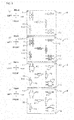
- FIG. 3A shows a top view of a substrate before being carried into the solder printing machine.
- FIG. 3B shows a top view of the substrate after being carried out from the solder printing machine.
- FIG. 3C shows a top view of the substrate after being carried out from the electronic component mounting machine.
- FIG. 3D shows a top view of the substrate after being carried out from the reflow furnace.
- FIG. 3B to FIG. 3D show the case where a printed state of solder portions 82 in the solder printing machine 3 shown in FIG. 1 is acceptable.
- a plurality of wiring patterns 80 and a plurality of substrate marks F1 to F3 are already printed on the substrate 8 before the substrate is carried into the solder printing machine 3 shown in FIG. 1 .
- the wiring patterns 80 include land portions 800.
- the plurality of wiring patterns 80 and the plurality of substrate marks F1 to F3 are printed at the same time. Therefore, the plurality of wiring patterns 80 and the plurality of substrate marks F1 to F3 are arranged in the same coordinate system.
- solder portions 82 are printed on the substrate 8 after the substrate is carried out from the solder printing machine 3 shown in FIG. 1 .
- predetermined solder portions 82 are used as solder paste marks f1 to f4.
- the plurality of solder portions 82 are printed simultaneously by the same screen mask. Therefore, the plurality of solder portions 82 and the plurality of solder paste marks f1 to f4 are arranged in the same coordinate system.
- the solder portions 82 (including the solder paste marks f1 to f4) are printed to be deviated from the land portions 800. However, the printed state of all the solder paste marks f1 to f4 is acceptable.
- a plurality of electronic components P1 to P6 are mounted on the substrate 8 after the substrate passes through all the electronic component mounting machines 5 shown in FIG. 1 .
- the mounting positions of all the electronic components P1 to P6 are determined with reference to the solder paste marks f1 to f4 in which the printed state is acceptable. Therefore, the plurality of electronic components P1 to P6 are accurately mounted with respect to the solder portions 82.
- the plurality of electronic components P1 to P6 and the solder portions 82 are arranged to be deviated from the land portions 800.
- the deviation of the plurality of electronic components P1 to P6 and the solder portions 82 with respect to the land portions 800 is eliminated by the self-alignment effect described above. That is, the plurality of electronic components P1 to P6 and the solder portions 82 are accurately arranged with respect to the land portions 800.
- the mounting position determination method is executed when the mounting positions of the electronic components P1 to P6 shown in FIG. 3D are determined in the electronic component mounting machine 5 shown in FIG. 1 .
- FIG. 4 shows a flowchart of the mounting position determination method.
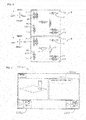
- FIG. 5A shows a top view of the substrate after being carried out from the solder printing machine.
- FIG. 5B shows a top view of the substrate after being carried out from the electronic component mounting machine at the upstream end in the transport direction.
- FIG. 6 shows a skip necessity inquiry screen.
- FIG. 5A corresponds to FIG. 3B
- FIG. 5B corresponds to FIG. 3C
- FIG. 5A and FIG. 5B show a case where the printed state of the solder portion 82 in the solder printing machine 3 is poor.
- the mounting position determination method includes a substrate mark reading step (S2 (step 2, the same applies hereinafter) in FIG. 46), a skip flag confirmation step (S4 in FIG. 4 ), a solder paste mark reading step (S5 in FIG. 4 ), and a skip necessity determination step (S9 to S11 in FIG. 4 ).
- the electronic components P1 and P2 among the electronic components P1 to P6 shown in FIG. 3D are mounted at predetermined positions on the substrate 8.
- the image-capturing device 571 of the first electronic component mounting machine 5 shown in FIG. 1 may firstly capture the images of the substrate marks F1 to F3 after an automatic operation is started (S1 in FIG. 4 ).
- the image processing device 503 processes the images of the substrate marks F1 to F3.
- the computer 502 reads the substrate marks F1 to F3 from the processed images (S2 in FIG. 4 ).
- the first electronic component mounting machine 5 starts capturing the images of and reading of the solder paste marks f 1 to f 4 (S3 in FIG. 4 ) .
- the solder portions 82 used as the solder paste marks f1 to f4 are determined in advance.
- the electronic component mounting machine 5 executes reading of the solder paste marks f1 to f4 in a predetermined order (in the order of f1 ⁇ f2 ⁇ f3 ⁇ f4 in this example).
- the computer 502 referring to the data stored in the memory section 502b, checks whether or not a skip flag is set for the solder paste mark f1 (S4 in FIG.4 ).
- the skip flag is set by the first electronic component mounting machine 5.
- the solder paste marks f1 to f4 on which the skip flag is set are not confirmed.
- the image-capturing device 571 captures the image of the solder paste mark f1.
- the positions of the solder paste marks f1 to f4 to be image-captured are each determined with reference to the substrate marks F1 to F3 that have been read in the substrate mark reading step (S2 in FIG. 4 ).
- the image processing device 503 processes an image of the solder paste mark f1.
- the computer 502 reads the solder paste mark f1 from the processed image (S5 in FIG. 4 ). Then, the computer 502 determines whether or not the solder paste mark f1 has been read (S6 in FIG. 4 ). As shown in FIG. 5A , the printed state of the solder paste mark f1 is acceptable. Therefore, the computer 502 can read the solder paste mark f1.
- the electronic component mounting machine 5 starts reading the solder paste mark f2, which is the next reading target (S7 and S3 in FIG. 4 ). Like the solder paste mark f1, the electronic component mounting machine 5 checks the skip flag of the solder paste mark f2 (S4 in FIG. 4 ), and captures the images of and executing reading of the solder paste mark f2 (S5 in FIG. 4 ). Then, the computer 502 determines whether or not the solder paste mark f2 has been read (S6 in FIG. 4 ).
- the display device 505 displays the skip necessity inquiry screen (S9 in FIG. 4 ). As shown in FIG. 6 , an inquiry message 505b about the necessity of skip, a skip determination button 505c, and a skip cancel button 505d are displayed on a screen 505a of the display device 505.
- An operator who visually recognizes the inquiry message 505b checks the image of the solder paste mark f2 through the screen of the display device 505.
- the operator determines that "the printed state of the solder paste mark f2 is acceptable"
- the operator corrects data related to the solder paste mark f2 via the screen of the display device 505.
- the operator touches the skip cancel button 505d (S10 in FIG. 4 ). That is, when the computer 502 cannot read the solder paste mark f2 even though the printed condition of the solder paste mark f2 is acceptable, it is assumed that there is some defect in the data related to the solder paste mark f2 in the memory section 502b (for example, an input error). Therefore, the operator checks the data, corrects the defect, and touches the skip cancel button 505d. Then, the computer 502 reads the solder paste mark f2 again (S5 in FIG. 4 ).
- the solder paste mark f2 is blurry. For this reason, the operator who has checked the image of the solder paste mark f2 touches the skip determination button 505c (S10 in FIG. 4 ). Then, the computer 502 sets a skip flag for the solder paste mark f2 that cannot be read (S11 in FIG. 4 ) .
- the information (skip flag) relating to the solder paste mark f2 is transmitted to the control device 50 of the electronic component mounting machine 5 on the downstream (subsequent) side in the transport direction shown in FIG. 1 .
- the skip flag is stored in the memory section 502b of the subsequent electronic component mounting machine 5.
- the electronic component mounting machine 5 reads the solder paste mark f3 (S7 ⁇ S3 ⁇ S4 ⁇ S5 ⁇ S6 in FIG. 4 ), and finally reads the solder paste mark f4 (S7 ⁇ S3 ⁇ S4 ⁇ S5 ⁇ S6 in FIG. 4 ).
- the computer 502 of the first electronic component mounting machine 5 determines the mounting positions of the electronic components P1 and P2 to be mounted by the electronic component mounting machine 5 (S8 in FIG. 4 ).
- the computer 502 determines the mounting position of the electronic component P1 with reference to the solder paste marks f1 and f3 in principle and with reference to the substrate marks F1 to F3 exceptionally. In addition, the mounting position of the electronic component P2 is determined with reference to the solder paste marks f2 and f4 in principle and with reference to the substrate marks F1 to F3 exceptionally.
- the computer 502 determines the mounting position of the electronic component P1 with reference to the two solder paste marks f1 and f3 at the diagonal positions. That is, the mounting position of the electronic component P1 stored in advance in the memory section 502b is corrected based on the deviation between the positions of the solder paste marks f1 and f3 stored in advance in the memory section 502b and the positions of the solder paste marks f1 and f3 actually read.
- the computer 502 determines the mounting position of the electronic component P1 with reference to the substrate marks F1 to F3, which are reference sources of the capturing-image positions of the solder paste marks f1 and f3. That is, the mounting position of the electronic component P1 stored in advance in the memory section 502b is corrected based on the deviation between the positions of the substrate marks F1 to F3 stored in advance in the memory section 502b and the positions of the substrate marks F1 to F3 actually read. As described above, the computer 502 determines the mounting position of the electronic component P1 with reference to the solder paste marks f1 and f3 in principle and with reference to the substrate marks F1 to F3 exceptionally. The same applies to the electronic component P2.
- the computer 502 determines the mounting position of the electronic component P1 with reference to the solder paste marks f1 and f3. On the other hand, since the solder paste mark f2 cannot be read, the computer 502 determines the mounting position of the electronic component P2 with reference to the substrate marks F1 to F3.
- the suction nozzle 570 shown in FIG. 2 mounts the electronic components P1 and P2 at the determined mounting coordinates. As shown in FIG. 5B , the electronic component P1 is accurately mounted on the solder portions 82. On the other hand, the electronic component P2 is accurately mounted on the land portions 800.
- the mounting position determination method shown in FIG. 4 is executed in the same manner as the first electronic component mounting machine 5.
- the skip flag for the unreadable solder paste mark f2 has already been transmitted from the first electronic component mounting machine 5 to the subsequent electronic component mounting machine 5.
- the computer 502 of the subsequent electronic component mounting machine 5 confirms the skip flag in the skip flag confirmation step (S4 in FIG. 4 ). For this reason, the computer 502 skips the imaging and reading of the solder paste mark f2. That is, in the subsequent electronic component mounting machine 5, imaging and reading are performed in the order of the solder paste marks f1 ⁇ f3 ⁇ f4. Note that the computer 502 of the subsequent electronic component mounting machine 5 determines the mounting position of the electronic component, which is scheduled to be determined with reference to the solder paste mark f 2, with reference to the substrate marks F 1 to F 3.
- the mounting positions of the electronic components P1 and P2 can be determined with reference to the solder paste marks f1 to f4 in principle and the substrate marks F1 to F3 exceptionally. That is, as shown in FIG. 4 , when the solder paste mark f2 cannot be read, the control device 50 automatically determines the mounting position of the electronic component P2 (specifically, the electronic component P2 of which the mounting position is determined with reference to the solder paste mark f2 which was not originally read) with reference to the substrate marks F1 to F3 that are the reference sources of the imaging position of the solder paste mark f2.
- the production of the substrate 8 can be automatically continued. Further, according to the electronic component mounting machine 5 of the embodiment, even when the control device 50 cannot read the solder paste mark f2 from the image, the manual operation of an operator (the operation of specifying the solder paste mark f2 of the print defect while viewing the image) does not intervene. Therefore, the accuracy of mounting the electronic component P2 is high.
- the subsequent electronic component mounting machine 5 can recognize the unreadable solder paste mark f2 by the information (skip flag) transmitted from the first electronic component mounting machine 5. Therefore, the subsequent electronic component mounting machine 5 can skip the imaging and reading of the unreadable solder paste mark f2. Therefore, in the subsequent electronic component mounting machine 5, it is possible to reduce the number of steps for imaging the marks and the number of steps for reading the marks.
- the display device 505 of the first electronic component mounting machine 5 displays the inquiry message 505b. Therefore, an operator who visually recognizes the inquiry can check the cause why the solder paste mark f2 cannot be read. If the computer 502 is unable to read the solder paste mark f2 even though the printed condition of the solder paste mark f2 is acceptable, it is assumed that there is some defect in the data related to the solder paste mark f2 in the memory section 502b (for example, an input error). In this regard, since the display device 505 displays the inquiry message 505b, the operator can easily find and correct the defect.
- the solder paste marks f1 to f4 for determining the mounting positions of the electronic components P1 and P2 are not particularly limited.
- the mounting position of the electronic component P1 may be determined from at least one of the solder paste marks f1 to f4 on the substrate 8. The same applies to the electronic component P2.
- the solder paste marks f1 to f4 for determining the mounting positions of the plurality of electronic components P1 and P2 may be completely coincident with each other. Alternatively, only a part of the solder paste marks may be coincident with each other. Alternatively, the solder paste marks may be quite different from each other.
- a single one of the solder paste marks f1 to f4 may be set based on the plurality of solder portions 82.
- the center of gravity of an imaginary quadrangle formed by connecting the outer edges of the four solder portions 82 at the left rear corner of FIG. 5A may be set as the solder paste mark f1.
- the solder paste mark f1 center of gravity
- the solder paste mark f1 center of gravity
- solder portions 82 dedicated to marks may be used in addition to the solder portions 82 for bonding the electronic components. That is, the solder paste marks f1 to f4 may be in the same coordinate system as the solder portions 82.
- the substrate marks F1 to F3 for determining the imaging positions of the solder paste marks f1 to f4 are not particularly limited.
- the mounting position of the solder paste mark f1 may be determined from at least one of the substrate marks F1 to F3. The same applies to the solder paste marks f2 to f4.
- the substrate marks F1 to F3 for determining the imaging positions of the plurality of solder paste marks f1 to f4 may be completely coincident with each other. Alternatively, only a part of the substrate marks may be coincident with each other. Alternatively, the solder paste marks may be quite different from each other.
- the land portions 800 may be used as the substrate marks F1 to F3. That is, the substrate marks F1 to F3 may be in the same coordinate system as the wiring patterns 80.
- Types of marks for the main fiducial mark and the sub-fiducial mark are not particularly limited.
- the type may be a character, a graphic, a symbol, a combination thereof, or the like.
- the numbers and the locations of the main fiducial marks and the sub-fiducial marks are not particularly limited.
- the type of the main fiducial mark is not particularly limited.
- the type of the main fiducial mark may be, in addition to the solder paste marks f1 to f4, a component mark (for example, a mark on an electronic component used for determining the mounting position when another electronic component is mounted on the upper surface of the electronic component) or the like.
- the type of the substrate 8 is not particularly limited.
- a plurality of divisible product substrates may be arranged on a single sheet substrate.
- the main fiducial mark may be disposed on at least one of the sheet substrate and the product substrate. The same applies to the sub-fiducial mark.
- the type of the image-capturing device 571 is not particularly limited.
- the type may be a CMOS (Complementary Metal-Oxide Semiconductor) camera.
- the types, the arrangement, and the numbers of the devices constituting the production line 1 are not particularly limited.
- the solder printing inspection machine 4 may not be arranged.
- 1 production line 3 : solder printing machine, 4 : solder printing inspection machine, 5 : electronic component mounting machine, 50 : control device, 500 : communication control circuit, 501 : input/output interface, 502 : computer, 502a: calculating section, 502b: memory section, 503 : image processing device, 505 : display device, 505a: screen, 505b: inquiry message, 505c: skip determination button, 505d: skip cancel button, 51 : component supply device, 510 : tape, 52 : substrate transport device, 520 : conveyor belt, 53 : X-axis guide rail, 54 : X-axis slide, 55 : Y-axis guide rail, 56 : Y-axis slide, 57: mounting head, 570: suction nozzle, 571: image-capturing device, 6: reflow furnace, 7: substrate appearance inspection machine, 8: substrate, 80: wiring pattern, 800: land portion, 82: solder portion, F1 to F3: substrate mark, P1 to
Landscapes
- Engineering & Computer Science (AREA)
- Manufacturing & Machinery (AREA)
- Microelectronics & Electronic Packaging (AREA)
- Operations Research (AREA)
- General Physics & Mathematics (AREA)
- Physics & Mathematics (AREA)
- Automation & Control Theory (AREA)
- Theoretical Computer Science (AREA)
- Computer Vision & Pattern Recognition (AREA)
- Health & Medical Sciences (AREA)
- Life Sciences & Earth Sciences (AREA)
- Chemical & Material Sciences (AREA)
- Analytical Chemistry (AREA)
- Biochemistry (AREA)
- General Health & Medical Sciences (AREA)
- Immunology (AREA)
- Pathology (AREA)
- Quality & Reliability (AREA)
- Supply And Installment Of Electrical Components (AREA)
Abstract
Description
- The present invention relates to an electronic component mounting machine for mounting electronic components on a substrate, and a production line in which a plurality of electronic component mounting machines are provided.
- A wiring pattern is printed on a substrate. A solder portion is printed on a land portion of the wiring pattern. For example, as disclosed in
Patent Literature 1, an electronic component mounting machine sometimes determines a mounting position of an electronic component with reference to a solder paste mark (solder portion). In this case, even if the solder portion is printed with being deviated from the land portion, the electronic component is mounted at a regular position with respect to the solder portion. At the time of reflow, the electronic component flows toward the center of the land portion together with the molten solder portion. Therefore, after the reflow, the electronic component can be mounted at the regular position as a result. In this manner, when the mounting position of the electronic component is determined with reference to the solder paste mark, the electronic component can be mounted at the regular position by relying on the self-alignment effect of the solder portion. - Patent Literature 1:
JP-A-2013-58605 - However, there are cases where the electronic component mounting machine cannot read the solder paste mark due to a print defect of the solder paste mark, or the like. In this case, the mounting position of the electronic component cannot be determined with reference to the solder paste mark. Therefore, conventionally, when the electronic component mounting machine cannot automatically read the solder paste mark, an operator manually specifies the solder paste mark of a print defect while viewing an image of the substrate. Then, the mounting position of the electronic component is determined with reference to the solder paste mark. However, in this case, if the skill level of an operator is low, the accuracy of mounting the electronic component becomes low. In addition, a solder portion having a shape similar to that of the solder paste mark may be printed on the substrate adjacent to the solder paste mark of a print defect. In this case, if the skill level of a worker is low, the worker may misrecognize the solder portion for the solder paste mark. As a result, the accuracy of mounting the electronic component is lowered. Therefore, an object of the invention is to provide an electronic component mounting machine and a production line having high accuracy of mounting an electronic component.
- In order to solve the above problems, an electronic component mounting machine according to the invention includes: an image-capturing device that captures images of a sub-fiducial mark, being disposed on a substrate, and a main fiducial mark of which imaging position is determined with reference to the sub-fiducial mark; and a control device that determines a mounting position of an electronic component with respect to the substrate with reference to the main fiducial mark when the main fiducial mark can be read from an image captured by the image-capturing device, while determines the mounting position with reference to the sub-fiducial mark, which is a reference source of the main fiducial mark, when the main fiducial mark cannot be read from the image due to a print defect of the main fiducial mark. Here, the "print defect" is a defect related to a defect at the time of printing the main fiducial mark, such as blur, chipping, bleeding, distortion, or the like.
- In order to solve the above problems, a production line according to the invention is a production line in which a plurality of the electronic component mounting machines are provided from an upstream toward a downstream in a transport direction of the substrate, wherein the control device of the electronic component mounting machine disposed at an upstream end in the transport direction transmits information related to the main fiducial mark, which cannot be read, to an electronic component mounting machine at the downstream in the transport direction when the main fiducial mark cannot be read from the image.
- According to the electronic component mounting machine of the invention, the mounting position of an electronic component can be determined with reference to the main fiducial mark in principle and with reference to the sub-fiducial mark exceptionally. That is, when the main fiducial mark cannot be read, the control device automatically determines the mounting position of the electronic component (specifically, the electronic component of which the mounting position is determined with reference to the main fiducial mark which was not originally read) with reference to the sub-fiducial mark which is the reference source of the main fiducial mark. Therefore, even when the main fiducial mark cannot be read, the production of the substrate can be automatically continued. Further, according to the electronic component mounting machine of the invention, even when the control device cannot read the main fiducial mark from the image, a manual operation of an operator (an operation of specifying the main fiducial mark of a print defect while viewing the image) does not intervene. Therefore, the accuracy of mounting the electronic component is high.
- In this manner, according to the production line of the invention, the electronic component mounting machine at the downstream in the transport direction can recognize the unreadable main fiducial mark by the information transmitted from the electronic component mounting machine on the upstream end in the transport direction. Therefore, the electronic component mounting machine at the downstream in the transport direction can skip reading of the unreadable main fiducial mark. Therefore, it is possible to reduce the number of steps for reading the marks in the electronic component mounting machine at the downstream in the transport direction.
-
- [
Fig. 1] FIG. 1 is a schematic diagram of a production line according to an embodiment of the invention. - [
Fig. 2] FIG. 2 is a top view of an electronic component mounting machine according to the embodiment of the invention. - [
Fig. 3A] FIG. 3A is a top view of a substrate before being carried into a solder printing machine.FIG. 3B is a top view of the substrate after being carried out from the solder printing machine.FIG. 3C is a top view of the substrate after being carried out from the electronic component mounting machine.FIG. 3D is a top view of the substrate after being carried out from a reflow furnace. - [
Fig. 4] FIG. 4 is a flowchart of a mounting position determination method. - [
Fig. 5A] FIG. 5A is a top view of the substrate after being carried out from the solder printing machine.FIG. 5B is a top view of the substrate after being carried out from the electronic component mounting machine at the upstream end in a transport direction. - [
Fig. 6] FIG. 6 is a skip necessity inquiry screen. - Hereinafter, an embodiment of an electronic component mounting machine and a production line according to the invention will be described.
- First, the configuration of the production line according to the embodiment will be described.
FIG. 1 is a schematic diagram of the production line according to the embodiment. As shown inFIG. 1 , theproduction line 1 includes asolder printing machine 3, a solderprinting inspection machine 4, a plurality of electroniccomponent mounting machines 5, a reflow furnace 6, and a substrateappearance inspection machine 7 from the left side (upstream in a transport direction) toward the right side (at downstream in the transport direction). These devices are communicatively connected. -
FIG. 2 is a top view of the electronic component mounting machine according to the embodiment. The configuration of a plurality of the electroniccomponent mounting machines 5 is the same. As shown inFIGS. 1 and 2 , the electroniccomponent mounting machine 5 includes acontrol device 50, acomponent supply device 51, asubstrate transport device 52, a pair of upper and lowerX-axis guide rails 53, anX-axis slide 54, a pair of left and right Y-axis guide rails 55, a Y-axis slide 56, and amounting head 57. - As shown in
FIG. 2 , thecomponent supply device 51 includes multiple tapes 510. The tape 510 accommodates electronic components. Thesubstrate transport device 52 includes a pair of front andrear conveyor belts 520. Asubstrate 8 is conveyed from the left side toward the right side by the pair of front andrear conveyor belts 520. The pair of left and right Y-axis guide rails 55 are disposed on an upper wall of a housing (not shown) of the electroniccomponent mounting machine 5. The Y-axis slide 56 is attached to the pair of left and right Y-axis guide rails 55 so as to be slidable in the front-rear direction. The pair of upper and lowerX-axis guide rails 53 are disposed on the Y-axis slide 56. TheX-axis slide 54 is attached to the pair of upper and lowerX-axis guide rails 53 so as to be slidable in the left-right direction. The mountinghead 57 is attached to theX-axis slide 54. Therefore, the mountinghead 57 is movable back and forth, left and right. The mountinghead 57 includes asuction nozzle 570 and an image-capturingdevice 571. Thesuction nozzle 570 is capable of transporting electronic components from thecomponent supply device 51 to thesubstrate 8. The image-capturingdevice 571 is a CCD (Charge-Coupled Device) camera. The image-capturingdevice 571 is capable of imaging the upper surface of thesubstrate 8. - As shown in
FIG. 1 , thecontrol device 50 includes a communication control circuit 500, an input/output interface 501, acomputer 502, animage processing device 503, and adisplay device 505. The input/output interface 501 is connected to the communication control circuit 500, thecomputer 502, theimage processing device 503, and thedisplay device 505. The communication control circuit 500 is connected to other devices constituting theproduction line 1. Thecomputer 502 includes a calculating section 502a and a memory section 502b. In the memory section 502b, data relating to wiring patterns, substrate marks, solder portions, solder paste marks, positions and shapes of electronic components, and the like, which will be described later, is stored in advance. Theimage processing device 503 is connected to the image-capturingdevice 571. Thedisplay device 505 is a touch screen (not shown). An operator can visually recognize information displayed on thedisplay device 505. Further, an operator can input an instruction to thedisplay device 505. - Next, a substrate production method executed by the production line according to the embodiment will be described.
FIG. 3A shows a top view of a substrate before being carried into the solder printing machine.FIG. 3B shows a top view of the substrate after being carried out from the solder printing machine.FIG. 3C shows a top view of the substrate after being carried out from the electronic component mounting machine.FIG. 3D shows a top view of the substrate after being carried out from the reflow furnace.FIG. 3B to FIG. 3D show the case where a printed state ofsolder portions 82 in thesolder printing machine 3 shown inFIG. 1 is acceptable. - As shown in
FIG. 3A , a plurality ofwiring patterns 80 and a plurality of substrate marks F1 to F3 are already printed on thesubstrate 8 before the substrate is carried into thesolder printing machine 3 shown inFIG. 1 . Thewiring patterns 80 includeland portions 800. The plurality ofwiring patterns 80 and the plurality of substrate marks F1 to F3 are printed at the same time. Therefore, the plurality ofwiring patterns 80 and the plurality of substrate marks F1 to F3 are arranged in the same coordinate system. - As shown in
FIG. 3B , a plurality of thesolder portions 82 are printed on thesubstrate 8 after the substrate is carried out from thesolder printing machine 3 shown inFIG. 1 . Of the plurality ofsolder portions 82,predetermined solder portions 82 are used as solder paste marks f1 to f4. The plurality ofsolder portions 82 are printed simultaneously by the same screen mask. Therefore, the plurality ofsolder portions 82 and the plurality of solder paste marks f1 to f4 are arranged in the same coordinate system. As shown in an exaggerated manner inFIG. 3B , the solder portions 82 (including the solder paste marks f1 to f4) are printed to be deviated from theland portions 800. However, the printed state of all the solder paste marks f1 to f4 is acceptable. - As shown in
FIG. 3C , a plurality of electronic components P1 to P6 are mounted on thesubstrate 8 after the substrate passes through all the electroniccomponent mounting machines 5 shown inFIG. 1 . The mounting positions of all the electronic components P1 to P6 are determined with reference to the solder paste marks f1 to f4 in which the printed state is acceptable. Therefore, the plurality of electronic components P1 to P6 are accurately mounted with respect to thesolder portions 82. On the other hand, the plurality of electronic components P1 to P6 and thesolder portions 82 are arranged to be deviated from theland portions 800. - As shown in
FIG. 3D , in thesubstrate 8 after being carried out from the reflow furnace 6 shown inFIG. 1 , the deviation of the plurality of electronic components P1 to P6 and thesolder portions 82 with respect to theland portions 800 is eliminated by the self-alignment effect described above. That is, the plurality of electronic components P1 to P6 and thesolder portions 82 are accurately arranged with respect to theland portions 800. - Next, a mounting position determination method executed in the substrate production method will be described. The mounting position determination method is executed when the mounting positions of the electronic components P1 to P6 shown in
FIG. 3D are determined in the electroniccomponent mounting machine 5 shown inFIG. 1 . -
FIG. 4 shows a flowchart of the mounting position determination method.FIG. 5A shows a top view of the substrate after being carried out from the solder printing machine.FIG. 5B shows a top view of the substrate after being carried out from the electronic component mounting machine at the upstream end in the transport direction.FIG. 6 shows a skip necessity inquiry screen. -
FIG. 5A corresponds toFIG. 3B , andFIG. 5B corresponds toFIG. 3C .FIG. 5A and FIG. 5B show a case where the printed state of thesolder portion 82 in thesolder printing machine 3 is poor. - As shown in
FIG. 4 , the mounting position determination method includes a substrate mark reading step (S2 (step 2, the same applies hereinafter) in FIG. 46), a skip flag confirmation step (S4 inFIG. 4 ), a solder paste mark reading step (S5 inFIG. 4 ), and a skip necessity determination step (S9 to S11 inFIG. 4 ). - In the first electronic
component mounting machine 5, the electronic components P1 and P2 among the electronic components P1 to P6 shown inFIG. 3D are mounted at predetermined positions on thesubstrate 8. As shown inFIG. 4 , the image-capturingdevice 571 of the first electroniccomponent mounting machine 5 shown inFIG. 1 may firstly capture the images of the substrate marks F1 to F3 after an automatic operation is started (S1 inFIG. 4 ). Theimage processing device 503 processes the images of the substrate marks F1 to F3. Thecomputer 502 reads the substrate marks F1 to F3 from the processed images (S2 inFIG. 4 ). - Next, the first electronic
component mounting machine 5 starts capturing the images of and reading of the solder paste marksf 1 to f 4 (S3 inFIG. 4 ) . Thesolder portions 82 used as the solder paste marks f1 to f4 are determined in advance. The electroniccomponent mounting machine 5 executes reading of the solder paste marks f1 to f4 in a predetermined order (in the order of f1 →f2 →f3 →f4 in this example). - The
computer 502, referring to the data stored in the memory section 502b, checks whether or not a skip flag is set for the solder paste mark f1 (S4 inFIG.4 ). Here, the skip flag is set by the first electroniccomponent mounting machine 5. Thus, in the first electroniccomponent mounting machine 5, the solder paste marks f1 to f4 on which the skip flag is set are not confirmed. - Subsequently, the image-capturing
device 571 captures the image of the solder paste mark f1. The positions of the solder paste marks f1 to f4 to be image-captured are each determined with reference to the substrate marks F1 to F3 that have been read in the substrate mark reading step (S2 inFIG. 4 ). - The
image processing device 503 processes an image of the solder paste mark f1. Thecomputer 502 reads the solder paste mark f1 from the processed image (S5 inFIG. 4 ). Then, thecomputer 502 determines whether or not the solder paste mark f1 has been read (S6 inFIG. 4 ). As shown inFIG. 5A , the printed state of the solder paste mark f1 is acceptable. Therefore, thecomputer 502 can read the solder paste mark f1. - In this case, the electronic
component mounting machine 5 starts reading the solder paste mark f2, which is the next reading target (S7 and S3 inFIG. 4 ). Like the solder paste mark f1, the electroniccomponent mounting machine 5 checks the skip flag of the solder paste mark f2 (S4 inFIG. 4 ), and captures the images of and executing reading of the solder paste mark f2 (S5 inFIG. 4 ). Then, thecomputer 502 determines whether or not the solder paste mark f2 has been read (S6 inFIG. 4 ). - Here, as shown by a dotted line in
FIG. 5A , the solder paste mark f2 is printed blurred. Printing blur is included in the concept of a "print defect" of the invention. Therefore, thecomputer 502 cannot read the solder paste mark f2. In this case, as shown inFIG. 6 , thedisplay device 505 displays the skip necessity inquiry screen (S9 inFIG. 4 ). As shown inFIG. 6 , an inquiry message 505b about the necessity of skip, a skip determination button 505c, and a skip cancel button 505d are displayed on a screen 505a of thedisplay device 505. - An operator who visually recognizes the inquiry message 505b checks the image of the solder paste mark f2 through the screen of the
display device 505. Here, if the operator determines that "the printed state of the solder paste mark f2 is acceptable", the operator corrects data related to the solder paste mark f2 via the screen of thedisplay device 505. Then, the operator touches the skip cancel button 505d (S10 inFIG. 4 ). That is, when thecomputer 502 cannot read the solder paste mark f2 even though the printed condition of the solder paste mark f2 is acceptable, it is assumed that there is some defect in the data related to the solder paste mark f2 in the memory section 502b (for example, an input error). Therefore, the operator checks the data, corrects the defect, and touches the skip cancel button 505d. Then, thecomputer 502 reads the solder paste mark f2 again (S5 inFIG. 4 ). - However, as shown by a dotted line in
FIG. 5A , in this example, the solder paste mark f2 is blurry. For this reason, the operator who has checked the image of the solder paste mark f2 touches the skip determination button 505c (S10 inFIG. 4 ). Then, thecomputer 502 sets a skip flag for the solder paste mark f2 that cannot be read (S11 inFIG. 4 ) . The information (skip flag) relating to the solder paste mark f2 is transmitted to thecontrol device 50 of the electroniccomponent mounting machine 5 on the downstream (subsequent) side in the transport direction shown inFIG. 1 . The skip flag is stored in the memory section 502b of the subsequent electroniccomponent mounting machine 5. - Subsequently, the electronic
component mounting machine 5 reads the solder paste mark f3 (S7 →S3 →S4 →S5 →S6 inFIG. 4 ), and finally reads the solder paste mark f4 (S7 →S3 →S4 →S5 →S6 inFIG. 4 ). When the reading of all the solder paste marks f1 to f4 is completed (S7 inFIG. 4 ), as shown inFIG. 5B , thecomputer 502 of the first electroniccomponent mounting machine 5 determines the mounting positions of the electronic components P1 and P2 to be mounted by the electronic component mounting machine 5 (S8 inFIG. 4 ). - The
computer 502 determines the mounting position of the electronic component P1 with reference to the solder paste marks f1 and f3 in principle and with reference to the substrate marks F1 to F3 exceptionally. In addition, the mounting position of the electronic component P2 is determined with reference to the solder paste marks f2 and f4 in principle and with reference to the substrate marks F1 to F3 exceptionally. - Hereinafter, a method of determining the mounting position of the electronic component P1 will be described as a representative example. When all of the solder paste marks f1 and f3 are read (S6 in
FIG. 4 ), thecomputer 502 determines the mounting position of the electronic component P1 with reference to the two solder paste marks f1 and f3 at the diagonal positions. That is, the mounting position of the electronic component P1 stored in advance in the memory section 502b is corrected based on the deviation between the positions of the solder paste marks f1 and f3 stored in advance in the memory section 502b and the positions of the solder paste marks f1 and f3 actually read. - On the other hand, when at least one of the solder paste marks f1 and f3 cannot be read (S6 in
FIG. 4 ), thecomputer 502 determines the mounting position of the electronic component P1 with reference to the substrate marks F1 to F3, which are reference sources of the capturing-image positions of the solder paste marks f1 and f3. That is, the mounting position of the electronic component P1 stored in advance in the memory section 502b is corrected based on the deviation between the positions of the substrate marks F1 to F3 stored in advance in the memory section 502b and the positions of the substrate marks F1 to F3 actually read. As described above, thecomputer 502 determines the mounting position of the electronic component P1 with reference to the solder paste marks f1 and f3 in principle and with reference to the substrate marks F1 to F3 exceptionally. The same applies to the electronic component P2. - In this example, since the solder paste marks f1 and f3 can be read, the
computer 502 determines the mounting position of the electronic component P1 with reference to the solder paste marks f1 and f3. On the other hand, since the solder paste mark f2 cannot be read, thecomputer 502 determines the mounting position of the electronic component P2 with reference to the substrate marks F1 to F3. - Thereafter, the
suction nozzle 570 shown inFIG. 2 mounts the electronic components P1 and P2 at the determined mounting coordinates. As shown inFIG. 5B , the electronic component P1 is accurately mounted on thesolder portions 82. On the other hand, the electronic component P2 is accurately mounted on theland portions 800. - Also in the subsequent electronic
component mounting machine 5 shown inFIG. 1 , the mounting position determination method shown inFIG. 4 is executed in the same manner as the first electroniccomponent mounting machine 5. However, the skip flag for the unreadable solder paste mark f2 has already been transmitted from the first electroniccomponent mounting machine 5 to the subsequent electroniccomponent mounting machine 5. Thecomputer 502 of the subsequent electroniccomponent mounting machine 5 confirms the skip flag in the skip flag confirmation step (S4 inFIG. 4 ). For this reason, thecomputer 502 skips the imaging and reading of the solder paste mark f2. That is, in the subsequent electroniccomponent mounting machine 5, imaging and reading are performed in the order of the solder paste marks f1 →f3 →f4. Note that thecomputer 502 of the subsequent electroniccomponent mounting machine 5 determines the mounting position of the electronic component, which is scheduled to be determined with reference to the solderpaste mark f 2, with reference to the substrate marksF 1 toF 3. - Next, the effects of the electronic component mounting machine and the production line according to the embodiment will be described. As shown in
FIGS. 5A and 5B , according to the electroniccomponent mounting machine 5 of the embodiment, the mounting positions of the electronic components P1 and P2 can be determined with reference to the solder paste marks f1 to f4 in principle and the substrate marks F1 to F3 exceptionally. That is, as shown inFIG. 4 , when the solder paste mark f2 cannot be read, thecontrol device 50 automatically determines the mounting position of the electronic component P2 (specifically, the electronic component P2 of which the mounting position is determined with reference to the solder paste mark f2 which was not originally read) with reference to the substrate marks F1 to F3 that are the reference sources of the imaging position of the solder paste mark f2. Therefore, even when the solder paste mark f2 cannot be read, the production of thesubstrate 8 can be automatically continued. Further, according to the electroniccomponent mounting machine 5 of the embodiment, even when thecontrol device 50 cannot read the solder paste mark f2 from the image, the manual operation of an operator (the operation of specifying the solder paste mark f2 of the print defect while viewing the image) does not intervene. Therefore, the accuracy of mounting the electronic component P2 is high. - Further, as shown in
FIG. 1 , according to theproduction line 1 of the embodiment, the subsequent electroniccomponent mounting machine 5 can recognize the unreadable solder paste mark f2 by the information (skip flag) transmitted from the first electroniccomponent mounting machine 5. Therefore, the subsequent electroniccomponent mounting machine 5 can skip the imaging and reading of the unreadable solder paste mark f2. Therefore, in the subsequent electroniccomponent mounting machine 5, it is possible to reduce the number of steps for imaging the marks and the number of steps for reading the marks. - As shown in
FIGS. 4 and5 , when thecontrol device 50 cannot read the solder paste mark f2, thedisplay device 505 of the first electroniccomponent mounting machine 5 displays the inquiry message 505b. Therefore, an operator who visually recognizes the inquiry can check the cause why the solder paste mark f2 cannot be read. If thecomputer 502 is unable to read the solder paste mark f2 even though the printed condition of the solder paste mark f2 is acceptable, it is assumed that there is some defect in the data related to the solder paste mark f2 in the memory section 502b (for example, an input error). In this regard, since thedisplay device 505 displays the inquiry message 505b, the operator can easily find and correct the defect. - The embodiment of the electronic component mounting machine and the production line according to the invention has been described above. However, the embodiment is not particularly limited to the above embodiment. Various modifications and improvements that can be made by those skilled in the art are possible.
- The solder paste marks f1 to f4 for determining the mounting positions of the electronic components P1 and P2 are not particularly limited. The mounting position of the electronic component P1 may be determined from at least one of the solder paste marks f1 to f4 on the
substrate 8. The same applies to the electronic component P2. The solder paste marks f1 to f4 for determining the mounting positions of the plurality of electronic components P1 and P2 may be completely coincident with each other. Alternatively, only a part of the solder paste marks may be coincident with each other. Alternatively, the solder paste marks may be quite different from each other. - A single one of the solder paste marks f1 to f4 may be set based on the plurality of
solder portions 82. For example, the center of gravity of an imaginary quadrangle formed by connecting the outer edges of the foursolder portions 82 at the left rear corner ofFIG. 5A may be set as the solder paste mark f1. In this case, when at least one of the foursolder portions 82 has the print defect, the solder paste mark f1 (center of gravity) may be determined to be unreadable. If the center of gravity can be calculated, the solder paste mark f1 (center of gravity) may be determined to be readable. For the solder paste marks f1 to f4,solder portions 82 dedicated to marks may be used in addition to thesolder portions 82 for bonding the electronic components. That is, the solder paste marks f1 to f4 may be in the same coordinate system as thesolder portions 82. - The substrate marks F1 to F3 for determining the imaging positions of the solder paste marks f1 to f4 are not particularly limited. The mounting position of the solder paste mark f1 may be determined from at least one of the substrate marks F1 to F3. The same applies to the solder paste marks f2 to f4. The substrate marks F1 to F3 for determining the imaging positions of the plurality of solder paste marks f1 to f4 may be completely coincident with each other. Alternatively, only a part of the substrate marks may be coincident with each other. Alternatively, the solder paste marks may be quite different from each other. The
land portions 800 may be used as the substrate marks F1 to F3. That is, the substrate marks F1 to F3 may be in the same coordinate system as thewiring patterns 80. - Types of marks for the main fiducial mark and the sub-fiducial mark are not particularly limited. For example, the type may be a character, a graphic, a symbol, a combination thereof, or the like. The numbers and the locations of the main fiducial marks and the sub-fiducial marks are not particularly limited. The type of the main fiducial mark is not particularly limited. The type of the main fiducial mark may be, in addition to the solder paste marks f1 to f4, a component mark (for example, a mark on an electronic component used for determining the mounting position when another electronic component is mounted on the upper surface of the electronic component) or the like.
- The type of the
substrate 8 is not particularly limited. For example, a plurality of divisible product substrates may be arranged on a single sheet substrate. In this case, the main fiducial mark may be disposed on at least one of the sheet substrate and the product substrate. The same applies to the sub-fiducial mark. - The type of the image-capturing
device 571 is not particularly limited. The type may be a CMOS (Complementary Metal-Oxide Semiconductor) camera. The types, the arrangement, and the numbers of the devices constituting theproduction line 1 are not particularly limited. For example, the solderprinting inspection machine 4 may not be arranged. - 1:production line 3 : solder printing machine, 4 : solder printing inspection machine, 5 : electronic component mounting machine, 50 : control device, 500 : communication control circuit, 501 : input/output interface, 502 : computer, 502a: calculating section, 502b: memory section, 503 : image processing device, 505 : display device, 505a: screen, 505b: inquiry message, 505c: skip determination button, 505d: skip cancel button, 51 : component supply device, 510 : tape, 52 : substrate transport device, 520 : conveyor belt, 53 : X-axis guide rail, 54 : X-axis slide, 55 : Y-axis guide rail, 56 : Y-axis slide, 57: mounting head, 570: suction nozzle, 571: image-capturing device, 6: reflow furnace, 7: substrate appearance inspection machine, 8: substrate, 80: wiring pattern, 800: land portion, 82: solder portion, F1 to F3: substrate mark, P1 to P6: electronic component, f1 to f4: solder paste mark
Claims (4)
- An electronic component mounting machine comprising:an image-capturing device that captures images of a sub-fiducial mark, being disposed on a substrate, and a main fiducial mark of which imaging position is determined with reference to the sub-fiducial mark; anda control device that determines a mounting position of an electronic component with respect to the substrate with reference to the main fiducial mark when the main fiducial mark can be read from an image captured by the image-capturing device, while determines the mounting position with reference to the sub-fiducial mark, which is a reference source of the main fiducial mark, when the main fiducial mark cannot be read from the image due to a print defect of the main fiducial mark.
- The electronic component mounting machine according to claim 1, wherein
the substrate has a land portion disposed on the substrate, a solder portion disposed on the land portion, a substrate mark having a same coordinate system as the land portion, and a solder paste mark having a same coordinate system as the solder portion, and wherein
the sub-fiducial mark is the substrate mark and the main fiducial mark is the solder paste mark. - A production line in which a plurality of the electronic component mounting machines according to claim 1 or claim 2 are provided from an upstream toward a downstream in a transport direction of the substrate, wherein
the control device of the electronic component mounting machine at an upstream end in the transport direction transmits information related to the main fiducial mark, which cannot be read, to the electronic component mounting machine at the downstream in the transport direction when the main fiducial mark cannot be read from the image. - The production line according to claim 3, wherein
the electronic component mounting machine at the upstream end in the transport direction includes a display device which displays inquires of an operator whether or not skipping of a reading operation is necessary when the control device cannot read the main fiducial mark from the image.
Applications Claiming Priority (1)
| Application Number | Priority Date | Filing Date | Title |
|---|---|---|---|
| PCT/JP2016/052623 WO2017130372A1 (en) | 2016-01-29 | 2016-01-29 | Electronic component mounting apparatus and production line |
Publications (3)
| Publication Number | Publication Date |
|---|---|
| EP3410834A1 true EP3410834A1 (en) | 2018-12-05 |
| EP3410834A4 EP3410834A4 (en) | 2019-01-23 |
| EP3410834B1 EP3410834B1 (en) | 2020-12-23 |
Family
ID=59397932
Family Applications (1)
| Application Number | Title | Priority Date | Filing Date |
|---|---|---|---|
| EP16887959.1A Active EP3410834B1 (en) | 2016-01-29 | 2016-01-29 | Electronic component mounting apparatus and production line |
Country Status (5)
| Country | Link |
|---|---|
| US (1) | US11291149B2 (en) |
| EP (1) | EP3410834B1 (en) |
| JP (1) | JP6669782B2 (en) |
| CN (1) | CN108476610B (en) |
| WO (1) | WO2017130372A1 (en) |
Families Citing this family (4)
| Publication number | Priority date | Publication date | Assignee | Title |
|---|---|---|---|---|
| WO2020240688A1 (en) * | 2019-05-28 | 2020-12-03 | Fuji Corporation | Fiducial mark allocation method, fiducial mark allocation device, mounting method and mounting system |
| JP7162573B2 (en) * | 2019-07-02 | 2022-10-28 | 日本発條株式会社 | stabilizer |
| JP7406571B2 (en) * | 2020-01-17 | 2023-12-27 | 株式会社Fuji | Inspection equipment and inspection method |
| TWI869737B (en) * | 2022-12-07 | 2025-01-11 | 易華電子股份有限公司 | Detection method of circuit board lead configuration |
Family Cites Families (15)
| Publication number | Priority date | Publication date | Assignee | Title |
|---|---|---|---|---|
| JPH0448248A (en) * | 1990-06-18 | 1992-02-18 | Hitachi Ltd | Cream solder printing inspection equipment |
| JP2000326495A (en) * | 1999-05-24 | 2000-11-28 | Matsushita Electric Ind Co Ltd | Inspection method for cream solder printing |
| JP4346827B2 (en) | 2001-03-06 | 2009-10-21 | パナソニック株式会社 | Electronic component mounting method |
| JP4676112B2 (en) | 2001-09-21 | 2011-04-27 | 富士機械製造株式会社 | Electric circuit manufacturing method and electric circuit manufacturing system |
| JP4493421B2 (en) * | 2004-06-30 | 2010-06-30 | 株式会社リコー | Printed circuit board inspection apparatus, printed circuit board assembly inspection line system, and program |
| JP2011029254A (en) * | 2009-07-22 | 2011-02-10 | Panasonic Corp | Electronic component mounting method |
| JP5229177B2 (en) * | 2009-10-08 | 2013-07-03 | パナソニック株式会社 | Component mounting system |
| JP5823174B2 (en) * | 2011-06-03 | 2015-11-25 | 富士機械製造株式会社 | Electronic component mounting position correction method and electronic component mounting position correction device |
| JP5767918B2 (en) * | 2011-09-08 | 2015-08-26 | 富士機械製造株式会社 | Electronic component mounting machine and electronic component mounting method |
| JP6065356B2 (en) * | 2011-09-26 | 2017-01-25 | 日本電気株式会社 | Defect inspection device, component mounting system, defect inspection method, program |
| JP2013074064A (en) | 2011-09-27 | 2013-04-22 | Hitachi High-Technologies Corp | Electronic component mounting apparatus and electronic component mounting method |
| JP5857190B2 (en) * | 2012-04-17 | 2016-02-10 | パナソニックIpマネジメント株式会社 | Electronic component mounting system |
| JP6018844B2 (en) * | 2012-08-30 | 2016-11-02 | ヤマハ発動機株式会社 | Component mounting method, component mounting apparatus, and program |
| JP5989803B2 (en) * | 2013-01-07 | 2016-09-07 | 富士機械製造株式会社 | Component mounting machine and component mounting method |
| JP6178978B2 (en) * | 2013-06-25 | 2017-08-16 | パナソニックIpマネジメント株式会社 | Electronic component mounting system and electronic component mounting method |
-
2016
- 2016-01-29 US US16/072,974 patent/US11291149B2/en active Active
- 2016-01-29 EP EP16887959.1A patent/EP3410834B1/en active Active
- 2016-01-29 WO PCT/JP2016/052623 patent/WO2017130372A1/en not_active Ceased
- 2016-01-29 JP JP2017563490A patent/JP6669782B2/en active Active
- 2016-01-29 CN CN201680079639.0A patent/CN108476610B/en active Active
Also Published As
| Publication number | Publication date |
|---|---|
| EP3410834A4 (en) | 2019-01-23 |
| WO2017130372A1 (en) | 2017-08-03 |
| JP6669782B2 (en) | 2020-03-18 |
| EP3410834B1 (en) | 2020-12-23 |
| US11291149B2 (en) | 2022-03-29 |
| CN108476610B (en) | 2020-05-15 |
| US20190029152A1 (en) | 2019-01-24 |
| CN108476610A (en) | 2018-08-31 |
| JPWO2017130372A1 (en) | 2018-11-22 |
Similar Documents
| Publication | Publication Date | Title |
|---|---|---|
| US20120189188A1 (en) | Component mounting system and mounting state inspection method in the component mounting system | |
| EP3410834B1 (en) | Electronic component mounting apparatus and production line | |
| JP5989803B2 (en) | Component mounting machine and component mounting method | |
| CN107432116B (en) | Mounting device, photographing processing method, and photographing unit | |
| US20080014772A1 (en) | Component mounting position correcting method and component mouting apparatus | |
| JP6734868B2 (en) | Image processing apparatus and image processing method for substrate | |
| JP4629584B2 (en) | Mounting system and electronic component mounting method | |
| EP3376844B1 (en) | Image processing device and image processing method for base plate | |
| JP5927504B2 (en) | Component mounting system and component mounting method | |
| EP2717665A1 (en) | Solder mark setting method and solder mark setting device | |
| EP3589105B1 (en) | Substrate working device and image processing method | |
| JP6706625B2 (en) | Board position search device and component mounter | |
| JP6890694B2 (en) | How to decide and how to wear | |
| JP6377136B2 (en) | Anti-substrate working machine, anti-substrate working system, and anti-substrate working method | |
| JP6948406B2 (en) | Electronic component mounting orientation confirmation system and electronic component mounting orientation confirmation method | |
| EP3315903B1 (en) | Board inspection apparatus | |
| JP2022073028A (en) | Component mounting system | |
| JP7503789B2 (en) | Component mounting error management device and component mounting device | |
| JP2017076728A (en) | Board working machine | |
| WO2024062635A1 (en) | Testing device and testing method | |
| JPWO2020016991A1 (en) | Inspection setting device and inspection setting method | |
| JP2007109937A (en) | Mounting state inspection method and apparatus |
Legal Events
| Date | Code | Title | Description |
|---|---|---|---|
| STAA | Information on the status of an ep patent application or granted ep patent |
Free format text: STATUS: THE INTERNATIONAL PUBLICATION HAS BEEN MADE |
|
| PUAI | Public reference made under article 153(3) epc to a published international application that has entered the european phase |
Free format text: ORIGINAL CODE: 0009012 |
|
| STAA | Information on the status of an ep patent application or granted ep patent |
Free format text: STATUS: REQUEST FOR EXAMINATION WAS MADE |
|
| 17P | Request for examination filed |
Effective date: 20180725 |
|
| AK | Designated contracting states |
Kind code of ref document: A1 Designated state(s): AL AT BE BG CH CY CZ DE DK EE ES FI FR GB GR HR HU IE IS IT LI LT LU LV MC MK MT NL NO PL PT RO RS SE SI SK SM TR |
|
| AX | Request for extension of the european patent |
Extension state: BA ME |
|
| A4 | Supplementary search report drawn up and despatched |
Effective date: 20190102 |
|
| RIC1 | Information provided on ipc code assigned before grant |
Ipc: H05K 13/08 20060101ALI20181218BHEP Ipc: H05K 13/04 20060101AFI20181218BHEP |
|
| RIN1 | Information on inventor provided before grant (corrected) |
Inventor name: SHIBATA, MITSUHIKO |
|
| DAV | Request for validation of the european patent (deleted) | ||
| DAX | Request for extension of the european patent (deleted) | ||
| GRAP | Despatch of communication of intention to grant a patent |
Free format text: ORIGINAL CODE: EPIDOSNIGR1 |
|
| STAA | Information on the status of an ep patent application or granted ep patent |
Free format text: STATUS: GRANT OF PATENT IS INTENDED |
|
| INTG | Intention to grant announced |
Effective date: 20200916 |
|
| GRAS | Grant fee paid |
Free format text: ORIGINAL CODE: EPIDOSNIGR3 |
|
| GRAA | (expected) grant |
Free format text: ORIGINAL CODE: 0009210 |
|
| STAA | Information on the status of an ep patent application or granted ep patent |
Free format text: STATUS: THE PATENT HAS BEEN GRANTED |
|
| AK | Designated contracting states |
Kind code of ref document: B1 Designated state(s): AL AT BE BG CH CY CZ DE DK EE ES FI FR GB GR HR HU IE IS IT LI LT LU LV MC MK MT NL NO PL PT RO RS SE SI SK SM TR |
|
| REG | Reference to a national code |
Ref country code: GB Ref legal event code: FG4D |
|
| REG | Reference to a national code |
Ref country code: DE Ref legal event code: R096 Ref document number: 602016050414 Country of ref document: DE |
|
| REG | Reference to a national code |
Ref country code: AT Ref legal event code: REF Ref document number: 1348984 Country of ref document: AT Kind code of ref document: T Effective date: 20210115 |
|
| REG | Reference to a national code |
Ref country code: IE Ref legal event code: FG4D |
|
| PG25 | Lapsed in a contracting state [announced via postgrant information from national office to epo] |
Ref country code: NO Free format text: LAPSE BECAUSE OF FAILURE TO SUBMIT A TRANSLATION OF THE DESCRIPTION OR TO PAY THE FEE WITHIN THE PRESCRIBED TIME-LIMIT Effective date: 20210323 Ref country code: RS Free format text: LAPSE BECAUSE OF FAILURE TO SUBMIT A TRANSLATION OF THE DESCRIPTION OR TO PAY THE FEE WITHIN THE PRESCRIBED TIME-LIMIT Effective date: 20201223 Ref country code: FI Free format text: LAPSE BECAUSE OF FAILURE TO SUBMIT A TRANSLATION OF THE DESCRIPTION OR TO PAY THE FEE WITHIN THE PRESCRIBED TIME-LIMIT Effective date: 20201223 Ref country code: GR Free format text: LAPSE BECAUSE OF FAILURE TO SUBMIT A TRANSLATION OF THE DESCRIPTION OR TO PAY THE FEE WITHIN THE PRESCRIBED TIME-LIMIT Effective date: 20210324 |
|
| REG | Reference to a national code |
Ref country code: AT Ref legal event code: MK05 Ref document number: 1348984 Country of ref document: AT Kind code of ref document: T Effective date: 20201223 |
|
| REG | Reference to a national code |
Ref country code: NL Ref legal event code: MP Effective date: 20201223 |
|
| PG25 | Lapsed in a contracting state [announced via postgrant information from national office to epo] |
Ref country code: BG Free format text: LAPSE BECAUSE OF FAILURE TO SUBMIT A TRANSLATION OF THE DESCRIPTION OR TO PAY THE FEE WITHIN THE PRESCRIBED TIME-LIMIT Effective date: 20210323 Ref country code: LV Free format text: LAPSE BECAUSE OF FAILURE TO SUBMIT A TRANSLATION OF THE DESCRIPTION OR TO PAY THE FEE WITHIN THE PRESCRIBED TIME-LIMIT Effective date: 20201223 Ref country code: SE Free format text: LAPSE BECAUSE OF FAILURE TO SUBMIT A TRANSLATION OF THE DESCRIPTION OR TO PAY THE FEE WITHIN THE PRESCRIBED TIME-LIMIT Effective date: 20201223 |
|
| PG25 | Lapsed in a contracting state [announced via postgrant information from national office to epo] |
Ref country code: NL Free format text: LAPSE BECAUSE OF FAILURE TO SUBMIT A TRANSLATION OF THE DESCRIPTION OR TO PAY THE FEE WITHIN THE PRESCRIBED TIME-LIMIT Effective date: 20201223 Ref country code: HR Free format text: LAPSE BECAUSE OF FAILURE TO SUBMIT A TRANSLATION OF THE DESCRIPTION OR TO PAY THE FEE WITHIN THE PRESCRIBED TIME-LIMIT Effective date: 20201223 |
|
| REG | Reference to a national code |
Ref country code: LT Ref legal event code: MG9D |
|
| PG25 | Lapsed in a contracting state [announced via postgrant information from national office to epo] |
Ref country code: EE Free format text: LAPSE BECAUSE OF FAILURE TO SUBMIT A TRANSLATION OF THE DESCRIPTION OR TO PAY THE FEE WITHIN THE PRESCRIBED TIME-LIMIT Effective date: 20201223 Ref country code: CZ Free format text: LAPSE BECAUSE OF FAILURE TO SUBMIT A TRANSLATION OF THE DESCRIPTION OR TO PAY THE FEE WITHIN THE PRESCRIBED TIME-LIMIT Effective date: 20201223 Ref country code: SM Free format text: LAPSE BECAUSE OF FAILURE TO SUBMIT A TRANSLATION OF THE DESCRIPTION OR TO PAY THE FEE WITHIN THE PRESCRIBED TIME-LIMIT Effective date: 20201223 Ref country code: LT Free format text: LAPSE BECAUSE OF FAILURE TO SUBMIT A TRANSLATION OF THE DESCRIPTION OR TO PAY THE FEE WITHIN THE PRESCRIBED TIME-LIMIT Effective date: 20201223 Ref country code: SK Free format text: LAPSE BECAUSE OF FAILURE TO SUBMIT A TRANSLATION OF THE DESCRIPTION OR TO PAY THE FEE WITHIN THE PRESCRIBED TIME-LIMIT Effective date: 20201223 Ref country code: PT Free format text: LAPSE BECAUSE OF FAILURE TO SUBMIT A TRANSLATION OF THE DESCRIPTION OR TO PAY THE FEE WITHIN THE PRESCRIBED TIME-LIMIT Effective date: 20210423 Ref country code: RO Free format text: LAPSE BECAUSE OF FAILURE TO SUBMIT A TRANSLATION OF THE DESCRIPTION OR TO PAY THE FEE WITHIN THE PRESCRIBED TIME-LIMIT Effective date: 20201223 |
|
| PG25 | Lapsed in a contracting state [announced via postgrant information from national office to epo] |
Ref country code: AT Free format text: LAPSE BECAUSE OF FAILURE TO SUBMIT A TRANSLATION OF THE DESCRIPTION OR TO PAY THE FEE WITHIN THE PRESCRIBED TIME-LIMIT Effective date: 20201223 Ref country code: PL Free format text: LAPSE BECAUSE OF FAILURE TO SUBMIT A TRANSLATION OF THE DESCRIPTION OR TO PAY THE FEE WITHIN THE PRESCRIBED TIME-LIMIT Effective date: 20201223 |
|
| REG | Reference to a national code |
Ref country code: CH Ref legal event code: PL |
|
| REG | Reference to a national code |
Ref country code: DE Ref legal event code: R097 Ref document number: 602016050414 Country of ref document: DE |
|
| PG25 | Lapsed in a contracting state [announced via postgrant information from national office to epo] |
Ref country code: MC Free format text: LAPSE BECAUSE OF FAILURE TO SUBMIT A TRANSLATION OF THE DESCRIPTION OR TO PAY THE FEE WITHIN THE PRESCRIBED TIME-LIMIT Effective date: 20201223 Ref country code: IS Free format text: LAPSE BECAUSE OF FAILURE TO SUBMIT A TRANSLATION OF THE DESCRIPTION OR TO PAY THE FEE WITHIN THE PRESCRIBED TIME-LIMIT Effective date: 20210423 Ref country code: LU Free format text: LAPSE BECAUSE OF NON-PAYMENT OF DUE FEES Effective date: 20210129 |
|
| REG | Reference to a national code |
Ref country code: BE Ref legal event code: MM Effective date: 20210131 |
|
| PG25 | Lapsed in a contracting state [announced via postgrant information from national office to epo] |
Ref country code: AL Free format text: LAPSE BECAUSE OF FAILURE TO SUBMIT A TRANSLATION OF THE DESCRIPTION OR TO PAY THE FEE WITHIN THE PRESCRIBED TIME-LIMIT Effective date: 20201223 Ref country code: IT Free format text: LAPSE BECAUSE OF FAILURE TO SUBMIT A TRANSLATION OF THE DESCRIPTION OR TO PAY THE FEE WITHIN THE PRESCRIBED TIME-LIMIT Effective date: 20201223 |
|
| PLBE | No opposition filed within time limit |
Free format text: ORIGINAL CODE: 0009261 |
|
| STAA | Information on the status of an ep patent application or granted ep patent |
Free format text: STATUS: NO OPPOSITION FILED WITHIN TIME LIMIT |
|
| GBPC | Gb: european patent ceased through non-payment of renewal fee |
Effective date: 20210323 |
|
| PG25 | Lapsed in a contracting state [announced via postgrant information from national office to epo] |
Ref country code: LI Free format text: LAPSE BECAUSE OF NON-PAYMENT OF DUE FEES Effective date: 20210131 Ref country code: DK Free format text: LAPSE BECAUSE OF FAILURE TO SUBMIT A TRANSLATION OF THE DESCRIPTION OR TO PAY THE FEE WITHIN THE PRESCRIBED TIME-LIMIT Effective date: 20201223 Ref country code: CH Free format text: LAPSE BECAUSE OF NON-PAYMENT OF DUE FEES Effective date: 20210131 |
|
| 26N | No opposition filed |
Effective date: 20210924 |
|
| PG25 | Lapsed in a contracting state [announced via postgrant information from national office to epo] |
Ref country code: IE Free format text: LAPSE BECAUSE OF NON-PAYMENT OF DUE FEES Effective date: 20210129 Ref country code: FR Free format text: LAPSE BECAUSE OF NON-PAYMENT OF DUE FEES Effective date: 20210223 Ref country code: GB Free format text: LAPSE BECAUSE OF NON-PAYMENT OF DUE FEES Effective date: 20210323 Ref country code: ES Free format text: LAPSE BECAUSE OF FAILURE TO SUBMIT A TRANSLATION OF THE DESCRIPTION OR TO PAY THE FEE WITHIN THE PRESCRIBED TIME-LIMIT Effective date: 20201223 |
|
| PG25 | Lapsed in a contracting state [announced via postgrant information from national office to epo] |
Ref country code: SI Free format text: LAPSE BECAUSE OF FAILURE TO SUBMIT A TRANSLATION OF THE DESCRIPTION OR TO PAY THE FEE WITHIN THE PRESCRIBED TIME-LIMIT Effective date: 20201223 |
|
| PG25 | Lapsed in a contracting state [announced via postgrant information from national office to epo] |
Ref country code: IS Free format text: LAPSE BECAUSE OF FAILURE TO SUBMIT A TRANSLATION OF THE DESCRIPTION OR TO PAY THE FEE WITHIN THE PRESCRIBED TIME-LIMIT Effective date: 20210423 |
|
| PG25 | Lapsed in a contracting state [announced via postgrant information from national office to epo] |
Ref country code: BE Free format text: LAPSE BECAUSE OF NON-PAYMENT OF DUE FEES Effective date: 20210131 |
|
| P01 | Opt-out of the competence of the unified patent court (upc) registered |
Effective date: 20230328 |
|
| PG25 | Lapsed in a contracting state [announced via postgrant information from national office to epo] |
Ref country code: CY Free format text: LAPSE BECAUSE OF FAILURE TO SUBMIT A TRANSLATION OF THE DESCRIPTION OR TO PAY THE FEE WITHIN THE PRESCRIBED TIME-LIMIT Effective date: 20201223 |
|
| PG25 | Lapsed in a contracting state [announced via postgrant information from national office to epo] |
Ref country code: HU Free format text: LAPSE BECAUSE OF FAILURE TO SUBMIT A TRANSLATION OF THE DESCRIPTION OR TO PAY THE FEE WITHIN THE PRESCRIBED TIME-LIMIT; INVALID AB INITIO Effective date: 20160129 |
|
| PG25 | Lapsed in a contracting state [announced via postgrant information from national office to epo] |
Ref country code: MK Free format text: LAPSE BECAUSE OF FAILURE TO SUBMIT A TRANSLATION OF THE DESCRIPTION OR TO PAY THE FEE WITHIN THE PRESCRIBED TIME-LIMIT Effective date: 20201223 |
|
| PG25 | Lapsed in a contracting state [announced via postgrant information from national office to epo] |
Ref country code: MT Free format text: LAPSE BECAUSE OF FAILURE TO SUBMIT A TRANSLATION OF THE DESCRIPTION OR TO PAY THE FEE WITHIN THE PRESCRIBED TIME-LIMIT Effective date: 20201223 |
|
| PG25 | Lapsed in a contracting state [announced via postgrant information from national office to epo] |
Ref country code: TR Free format text: LAPSE BECAUSE OF FAILURE TO SUBMIT A TRANSLATION OF THE DESCRIPTION OR TO PAY THE FEE WITHIN THE PRESCRIBED TIME-LIMIT Effective date: 20201223 |
|
| PGFP | Annual fee paid to national office [announced via postgrant information from national office to epo] |
Ref country code: DE Payment date: 20251203 Year of fee payment: 11 |