EP3376844B1 - Image processing device and image processing method for base plate - Google Patents
Image processing device and image processing method for base plate Download PDFInfo
- Publication number
- EP3376844B1 EP3376844B1 EP15908293.2A EP15908293A EP3376844B1 EP 3376844 B1 EP3376844 B1 EP 3376844B1 EP 15908293 A EP15908293 A EP 15908293A EP 3376844 B1 EP3376844 B1 EP 3376844B1
- Authority
- EP
- European Patent Office
- Prior art keywords
- mark
- board
- alternative
- fiducial mark
- fiducial
- Prior art date
- Legal status (The legal status is an assumption and is not a legal conclusion. Google has not performed a legal analysis and makes no representation as to the accuracy of the status listed.)
- Active
Links
- 238000012545 processing Methods 0.000 title claims description 59
- 238000003672 processing method Methods 0.000 title claims description 9
- 238000003384 imaging method Methods 0.000 claims description 26
- 238000001514 detection method Methods 0.000 claims description 25
- 238000000034 method Methods 0.000 description 51
- 230000008569 process Effects 0.000 description 48
- 238000004519 manufacturing process Methods 0.000 description 18
- 238000003860 storage Methods 0.000 description 10
- 238000012546 transfer Methods 0.000 description 8
- 230000000694 effects Effects 0.000 description 4
- 239000000047 product Substances 0.000 description 4
- 238000010586 diagram Methods 0.000 description 3
- 230000003287 optical effect Effects 0.000 description 3
- 238000004891 communication Methods 0.000 description 2
- 230000007246 mechanism Effects 0.000 description 2
- 230000015654 memory Effects 0.000 description 2
- 238000002360 preparation method Methods 0.000 description 2
- 230000004044 response Effects 0.000 description 2
- 230000002159 abnormal effect Effects 0.000 description 1
- 230000000295 complement effect Effects 0.000 description 1
- 230000001419 dependent effect Effects 0.000 description 1
- 238000000605 extraction Methods 0.000 description 1
- 238000001914 filtration Methods 0.000 description 1
- 230000006870 function Effects 0.000 description 1
- 230000001788 irregular Effects 0.000 description 1
- 238000005259 measurement Methods 0.000 description 1
- 229910044991 metal oxide Inorganic materials 0.000 description 1
- 150000004706 metal oxides Chemical class 0.000 description 1
- 239000004065 semiconductor Substances 0.000 description 1
- 229910000679 solder Inorganic materials 0.000 description 1
- 239000013589 supplement Substances 0.000 description 1
- 230000007704 transition Effects 0.000 description 1
- 230000000007 visual effect Effects 0.000 description 1
Images

Classifications
-
- H—ELECTRICITY
- H05—ELECTRIC TECHNIQUES NOT OTHERWISE PROVIDED FOR
- H05K—PRINTED CIRCUITS; CASINGS OR CONSTRUCTIONAL DETAILS OF ELECTRIC APPARATUS; MANUFACTURE OF ASSEMBLAGES OF ELECTRICAL COMPONENTS
- H05K13/00—Apparatus or processes specially adapted for manufacturing or adjusting assemblages of electric components
- H05K13/08—Monitoring manufacture of assemblages
- H05K13/081—Integration of optical monitoring devices in assembly lines; Processes using optical monitoring devices specially adapted for controlling devices or machines in assembly lines
- H05K13/0815—Controlling of component placement on the substrate during or after manufacturing
-
- H—ELECTRICITY
- H05—ELECTRIC TECHNIQUES NOT OTHERWISE PROVIDED FOR
- H05K—PRINTED CIRCUITS; CASINGS OR CONSTRUCTIONAL DETAILS OF ELECTRIC APPARATUS; MANUFACTURE OF ASSEMBLAGES OF ELECTRICAL COMPONENTS
- H05K13/00—Apparatus or processes specially adapted for manufacturing or adjusting assemblages of electric components
- H05K13/08—Monitoring manufacture of assemblages
- H05K13/081—Integration of optical monitoring devices in assembly lines; Processes using optical monitoring devices specially adapted for controlling devices or machines in assembly lines
- H05K13/0812—Integration of optical monitoring devices in assembly lines; Processes using optical monitoring devices specially adapted for controlling devices or machines in assembly lines the monitoring devices being integrated in the mounting machine, e.g. for monitoring components, leads, component placement
Definitions
- the present invention relates to a board image processing device and a board image processing method.
- PTL 1 discloses a configuration of recognizing a reference position of a board loaded in a component mounting machine. For example, in the recognition of the reference position of the board, a wiring pattern of the board is imaged and a characteristic section in the wiring pattern is detected as a fiducial mark from acquired image data. In addition, in the detection described above, a template showing the characteristic section in the wiring pattern is used, the template using reference lines formed from a shape that follows edge sections of the characteristic section and multiple seek lines which intersect with the edge sections.
- PTL 1 JP-A-2003-086996 Further examples of board image processing are disclosed in US 2002/168097 A1 , US 2006/048383 A1 , JP 2009 170516 A and JP H04 340799 A .
- an image processing device displays the image data for an operator so that the operator can set the reference position in the image data to be used during the detection process.
- setting of the reference position through a manual operation performed by an operator will contain an error due to visual measurement being used.
- the present invention is made in consideration of such circumstances, and an object thereof is to provide a board image processing device and a board image processing method in which it is possible to recognize a reference position of the board with higher accuracy.
- any characteristic section other than the fiducial mark of one or multiple of the characteristic sections in the wiring pattern can be acquired as an alternative mark, and a supplementary process using the alternative mark can be performed.
- the reference position of the board is automatically recognized, it is possible to recognize the reference position with high accuracy, compared to a case where the reference position of the board is set through a manual operation performed by the operator. Accordingly, by performing the supplementary process in a mounting process performed by a component mounting machine, it is possible to optimally maintain accuracy of the mounting process.
- a board image processing device of the present invention will be described with reference to the figures.
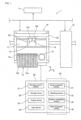
- an example configuration is given in which a board image processing device is installed in a component mounting machine that configures a production line for manufacturing a circuit board product such as an integrated circuit is.
- production line 1 is configured with multiple production equipments that are connected to host computer 2 via a network such that communication between them is possible.
- Examples of production equipment include a screen printer, a mounting inspector, a reflow oven, or the like, in addition to component mounting machine 10.
- the production equipment including component mounting machine 10 is configured to be capable of inputting and outputting various types of data to and from host computer 2 via the network.
- Host computer 2 monitors an operating state of production line 1 and controls the production equipment including component mounting machine 10.
- Host computer 2 stores various types of data for controlling component mounting machine 10.
- the various types of data include a production plan including a type and amount of a circuit board product to be produced, a control program for causing component mounting machine 10 to operate, and a template that is used in an image processing.
- Host computer 2 appropriately transmits various types of data such as the control program to the production equipment during execution of a production process by the production equipment.
- multiple component mounting machines 10 that configure production line 1 include board conveyance device 11, component supply device 12, component transfer device 13, component camera 14, board camera 15, and control device 20.
- a horizontal width direction (left-right direction in Fig. 1 ) of component mounting machine 10 is referred to as an X-axis direction
- a horizontal depth direction (up-down direction in Fig. 1 ) of component mounting machine 10 is referred to as a Y-axis direction
- a vertical direction (front-rear direction in Fig. 1 ) perpendicular to the X-axis direction and the Y-axis direction is referred to as a Z-axis direction.
- Board conveyance device 11 is configured with a belt conveyor and conveys boards 50 in a conveyance direction (X-axis direction in the embodiment) in a sequential order. Board conveyance device 11 positions board 50 at a predetermined position in component mounting machine 10. Board conveyance device 11 conveys the board 50 out of component mounting machine 10 after the mounting process is executed by component mounting machine 10.
- Component supply device 12 supplies electronic components, which are mounted on board 50, at a supply position Ps.
- Component supply device 12 is provided with multiple slots aligned in the X-axis direction. The multiple slots are all set such that a feeder 12a can be attached and detached.
- component supply device 12 causes feeder 12a to feed and move a carrier tape so as to supply an electronic component at a pickup section positioned on a front end side (upper side in Fig. 1 ) of feeder 12a.
- Component transfer device 13 is configured to be capable of moving in the X-axis direction and the Y-axis direction.
- Component transfer device 13 is disposed from a rear side (upper side in Fig. 1 ) of component mounting machine 10 in the depth direction to a position above component supply device 12 on a front side.
- Component transfer device 13 includes head driving device 13a, moving table 13b, and mounting head 13c.
- Head driving device 13a has a configuration in which a linear motion mechanism causes moving table 13b to be movable in the XY-axis directions.
- Mounting head 13c is clamped to be fixed to moving table 13b via a frame (not illustrated).
- multiple suction nozzles (not illustrated) are detachably provided on mounting head 13c.
- Mounting head 13c supports the suction nozzles in a liftable/lowerable manner and in a rotatable manner around an R-axis that is parallel to the Z-axis.
- a lifting and lowering position and an angle with respect to the mounting head 13c, and a supply state of negative pressure of the suction nozzles are controlled. By negative pressure being supplied to the suction nozzles, the suction nozzles pick up and hold an electronic component that is supplied at the pickup section of feeder 12a.
- Component camera 14 and board camera 15 are digital imaging devices having an imaging element such as a charge coupled device (CCD) or a complementary metal oxide semiconductor (CMOS) .
- Component camera 14 and board camera 15 perform imaging in a range of a camera field-of-view, based on a control signal by control device 20, which is connected to be capable of communicating, and transmit image data acquired by the imaging to control device 20.
- CCD charge coupled device
- CMOS complementary metal oxide semiconductor
- Component camera 14 is fixed to a base of component mounting machine 10 such that an optical axis is formed upward in the vertical direction (Z-axis direction) , and is configured to be capable of performing the imaging from below component transfer device 13. More specifically, component camera 14 is configured to be capable of imaging a lower face of the electronic component that is in a state of being held by the suction nozzle. Board camera 15 is provided on moving table 13b of component transfer device 13 such that an optical axis is formed downward in the vertical direction (Z-axis direction) . Board camera 15 is configured to be capable of imaging board 50.
- Control device 20 is configured with mainly a CPU, various types of memories, and a control circuit. Control device 20 controls a mounting process of the electronic component. Control device 20 is connected to the host computer 2 via a network such that communication is possible. As illustrated in Fig. 1 , control device 20 includes mounting control section 21, storage device 22, display device 23, input device 24, and image processing device 30.
- Mounting control section 21 controls a position of mounting head 13c or motion of a suction mechanism. To be more exact, mounting control section 21 inputs results of various types of recognition processes and information that is output from various types of sensors provided on component mounting machine 10. Mounting control section 21 transmits a control signal to component transfer device 13, based on a control program stored in storage device 22, information obtained by the various types of sensors, and results of recognition processes performed by image processing device 30. In this manner, a position and a rotation angle of the suction nozzle supported by mounting head 13c are controlled.
- Storage device 22 is configured with an optical drive device such as a hard disk device, a flash memory, or the like. Storage device 22 stores the control program, control information, image data, temporary data of various types of processes performed by image processing device 30. Display device 23 displays the various types of data as an image for the operator. Input device 24 is a device that accepts the input of the various types of data through a manual operation performed by the operator.
- Image processing device 30 acquires image data obtained by imaging performed by component camera 14 and board camera 15 and executes appropriate image processing.
- the image processing can include binarization of the image data, filtering, hue extraction, super-resolution processing, or the like.
- Image processing device 30 executes the image processing for recognizing the reference position of board 50.
- control device 20 corrects the position of the suction nozzle that is held by mounting head 13c depending on a positioning state of board 50, based on the results of the image processing for recognizing the reference position of the board 50. In this manner, the electronic component is mounted at an optimal position of the board 50, and accuracy of the mounting process is improved.
- a detection process of a fiducial mark having a given shape, which is disposed on an upper face of the board 50 is performed.
- at least one of one or more characteristic sections contained in the wiring pattern formed on the upper face of the board is set as a fiducial mark indicating the reference position.
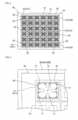
- the board 50 in the embodiment is a multi-unit board configured with multiple unit boards 51.
- the multi-unit board is divided into individual unit boards after the mounting of the electronic components to become multiple electronic circuit products that are the same.
- the same wiring pattern is formed on each of the multiple unit boards 51.
- the wiring pattern of unit board 51 is configured with lands 52 that are electrically connected to a terminal of the electronic component via solder that is applied through printing or the like.
- Land 52 of unit board 51 in the embodiment is configured from a combination of multiple rectangles and individually configures one wiring pattern and characteristic section 53 of the wiring pattern.
- characteristic sections 53 in five reference-use unit boards, 51A to 51E, which are selected by an operator from the total of 36 unit boards 51 are each set as fiducial marks indicating the reference positions of the board 50.
- the characteristic sections 53 of the reference-use unit boards 51A to 51E are also referred to as fiducial marks Mt.
- image processing device 30 includes image acquisition section 31, detecting section 32, position recognition section 35, and mark acquisition section 36.
- Image acquisition section 31 acquires first image data 60A obtained by imaging a region of the board 50 which includes the fiducial mark Mt.
- the "region including the fiducial mark Mt" means a region that can be imaged by board camera 15 that is relatively moved with respect to the board 50.
- Detecting section 32 detects a position of the fiducial mark Mt by scanning the first image data 60A by using template 70 (corresponding to a "first template” of the present invention) showing a shape of the fiducial mark Mt.
- the template 70 that is used in the detection process is configured with a reference line, which has a shape that follows edges section of the fiducial mark Mt which is a detection target, and multiple seek lines disposed based on the shape of the edge portions.
- the template is stored in storage device 22.
- the template 70 is configured with reference lines 71 having a shape that follows edge sections of the characteristic section 53, which is the fiducial mark Mt, and a specified point 72 indicating the position of the fiducial mark Mt in a case where the fiducial mark Mt is detected.
- a positional relationship between a position of the specified point 72 and the reference position of the board 50 is defined.
- Position recognition section 35 recognizes the reference position of the board 50, based on a result of detection of the fiducial mark Mt through scanning performed by detecting section 32 with the template 70.
- image processing device 30 needs to recognize the reference position of the board 50 by another method in a case where the position of the fiducial mark Mt is not detected through the scanning by using the template 70 described above.
- Image processing device 30 executes a supplementary process that supplements the detection process.
- mark acquisition section 36 acquires a different characteristic section 53 that is different from the fiducial mark Mt as an alternative mark Mb instead of the fiducial mark Mt.
- the alternative mark Mb which is a new detection target is one characteristic section 53 of the wiring pattern disposed on the upper face of the same board 50.
- the shape of the alternative mark Mb is not limited to the same shape as that of the fiducial mark Mt and may have an abnormal shape.
- the alternative mark Mb is the characteristic section 53 formed on another unit board 51, which is different from the unit boards 51A to 51E for reference, and has the same shape as that of the fiducial mark Mt.
- the image acquisition section 31 acquires second image data 60B obtained by imaging a region including the alternative mark Mb of the board 50.
- Detecting section 32 detects the position of the alternative mark Mb by scanning the second image data 60B by using a second template showing a shape of the alternative mark Mb.
- position recognition section 35 recognizes the reference position of the board 50 based on a result of detection performed by detecting section 32 and a positional relationship between the fiducial mark Mt and the alternative mark Mb.
- image acquisition section 31 acquires the first image data 60A as the second image data 60B.
- the first image data 60A and the second image data 60B are identical and are simply referred to as "image data 60".
- each of the fiducial mark Mt and the alternative mark Mb is set at the same position and has the same shape in the wiring pattern. Therefore, the second template used for the supplementary process can serve as the template 70 (first template) used for the scanning of the fiducial mark Mt, and the second template is the same as the template 70.
- Image acquisition section 31 having such a configuration as described above corresponds to a "first image acquisition section” and a “second image acquisition section” of the present invention.
- detecting section 32 corresponds to a “first detecting section” and a “second detecting section” of the present invention.
- Position recognition section 35 corresponds to a "first position recognition section” and a “second position recognition section” of the present invention.
- control device 20 serves as a display section that displays a portion or the entirety of the board 50 from the image data 60 in the supplementary process.
- input device 24 of control device 20 serves as a setting accepting section that accepts designation of the alternative mark Mb and an input of the positional relationship between the fiducial mark Mt and the alternative mark Mb by an operator.
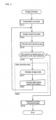
- Step 11 The image processing of recognizing the reference position of the board 50 by image processing device 30 for the board is described.
- the image processing is executed for recognizing the reference position of the board 50 positioned by board conveyance device 11 in the mounting process of component mounting machine 10.
- image processing device 30 executes a preparation process (Step 11 [hereinafter, "Step" is described as "S"]).
- the preparation process (S11) contains an imaging process of imaging a region containing the fiducial mark Mt of the board 50 or a reading process of reading the template 70 showing the shape of the fiducial mark Mt from storage device 22.
- image acquisition section 31 acquires, from storage device 22, the image data 60 obtained by imaging the fiducial mark Mt, as a first image acquiring step (S12) .
- detecting section 32 detects the position of the fiducial mark Mt by scanning the image data 60 by using the template 70 (S13).
- Image processing device 30 determines whether the position of the fiducial mark Mt has been detected through the scanning performed by detecting section 32 (S14) . Specifically, in a case where all of the reference lines 71 of the template 70 are coincident with the edge sections of the image data 60 at a predetermined position in the image data 60 subjected to edge processing, it is determined that the fiducial mark Mt coincident with the template 70 is detected (S14: Yes). As a first position recognizing step, the position recognition section 35 recognizes the reference position of the board 50, based on the result of detection of the fiducial mark Mt through scanning performed by detecting section 32 (S15).
- image processing device 30 determines that the position of the fiducial mark Mt is not detected (S14: No). As described above, in a case where it is not possible to detect the position of the fiducial mark Mt due to a factor such as absence of a part of the characteristic section 53 which is the fiducial mark Mt, the image processing device 30 executes the supplementary process by using the alternative mark Mb (S20 and S12 to S14).
- mark acquisition section 36 acquires a different characteristic section 53 that is different from the fiducial mark Mt as the alternative mark Mb instead of the fiducial mark Mt, as a mark acquiring step (S20). Specifically, as illustrated in Fig. 5 , the board 50 is displayed for the operator (S21). At this time, display device 23 may display the entire board 50 or may further enlarge and display a portion of the board 50 in response to a request of an operator. In addition, mark acquisition section 36 accepts designation of the alternative mark Mb and an input of the positional relationship between the fiducial mark Mt and the alternative mark Mb by an operator (S22).
- a region is designated so as to surround a unit board 51 adjacent to the unit board 51A in the X-direction (up-down direction in Fig. 5 ) which has a characteristic section 53 set as the fiducial mark Mt, through an operation of a pointer device, a touch operation on a screen, or the like by the operator.
- a designation region 61 containing the alternative mark Mb is set.
- the operator inputs information on a coordinate of the alternative mark Mb and information on types of alternative mark Mb.
- the board 50 is a multi-unit board, and storage device 22 stores a positional relationship between the multiple unit boards 51, that is, positional information indicating a distance in the XY-axis direction.
- the operator inputs how many unit boards 51 having the characteristic section 53 set as the alternative mark Mb are provided in the XY-axis directions with respect to the unit board 51A having the characteristic section 53 set as the fiducial mark Mt, and thereby mark acquisition section 36 is configured to establish a positional relationship between the fiducial mark Mt and the alternative mark Mb.
- the alternative mark Mb that is used in the supplementary process does not need to have the same shape as the fiducial mark Mt.
- mark acquisition section 36 accepts information on types of alternative mark Mb, and thereby is configured to acquire the alternative mark Mb corresponding to a type registered in advance.
- the board 50 is a multi-unit board, and the position and the shape of the characteristic section 53 in each of the unit boards 51 are the same as the fiducial mark Mt. Hence, it is possible to omit the input of the position and the shape of the alternative mark Mb in the acceptance of information on the alternative mark Mb (S22).
- the alternative mark Mb a characteristic section that is at another position and has another shape in the unit board 51 which is a target.
- the operator needs to input information indicating that the fiducial mark Mt and the alternative mark Mb are the same type and information indicating that the marks are at the same position, thereby designating that the fiducial mark Mt and the alternative mark Mb are the same characteristic section 53 in different unit boards 51.
- image acquisition section 31 acquires the image data corresponding to designation region 61 as a second image acquiring step (S12).
- the imaging process performed by board camera 15 is omitted, and image acquisition section 31 acquires the image data 60.
- image acquisition section 31 executes an imaging process performed by board camera 15.
- detecting section 32 detects the position of the alternative mark Mb through scanning of the image data 60 by using the second template (in the embodiment, the template 70 having two functions) showing the shape of the alternative mark Mb (S13). Detecting section 32 acquires the template 70 used in the first detecting step, as the second template that is used in the second detecting step, based on information indicating that the type of alternative mark Mb is the same as the type of fiducial mark Mt.
- Image processing device 30 determines whether the position of the alternative mark Mb has been detected through the scanning performed by detecting section 32 (S14). Specifically, in a case where all of the reference lines 71 of the template 70 are coincident with the edge sections of the image data 60 in designation region 61 designated by the operator, it is determined that the alternative mark Mb coincident with the template 70 is detected (S14; Yes).
- Position recognition section 35 recognizes the reference position of the board 50 based on the result of detection performed in the second detecting step (S13) and a positional relationship between the fiducial mark Mt and the alternative mark Mb, as a second position recognizing step (S15).
- image processing device 30 determines that the position of the alternative mark Mb has not been detected (S14 : No). As described above, in a case where the position of the alternative mark Mb cannot be detected, image processing device 30 re-executes the supplementary process by using the alternative mark Mb (S20 and S12 to S14).
- image processing device 30 executes the image processing of recognizing the reference position of the board 50, with the characteristic section 53 of the reference-use unit boards 51A to 51E which is designated first as the fiducial mark Mt.
- the supplementary process in which the alternative mark Mb is used in the image processing is an irregular process corresponding to a case where an undetectable characteristic section 53 is present, and it is determined with respect to each individual board 50 whether to perform the supplementary process.
- Configurations of an image processing device and an image processing method of the second embodiment are the same as those in the first embodiment, except for the mark acquiring step (S20) in the first embodiment.
- the other common configurations are substantially the same as those in the first embodiment, and thus detailed description is omitted.
- mark acquisition section 36 when a mark acquiring step (S120) is executed, mark acquisition section 36 first acquires candidate table 80 (S121).
- a candidate mark which is usable as the alternative mark Mb of multiple characteristic sections 53, is associated with a positional relationship (the "mark coordinate" column in Fig. 7 ) between the fiducial mark Mt and each of the multiple candidate marks .
- a type (the "type" column in Fig. 7 ) is associated as information on each shape of the candidate marks with the multiple candidate marks.
- mark acquisition section 36 acquires information on the fiducial mark Mt that was not detected through the scanning by using the template 70, as a first detecting step (S122). Specifically, mark acquisition section 36 identifies, from reference-use unit boards 51A to 51E, a unit board having undetectable fiducial mark Mt and acquires a position on the board 50 which is a multi-unit board. In this manner, as illustrated in Fig. 7 , a relationship between the fiducial mark Mt and the candidate mark is established.
- mark acquisition section 36 selects one candidate mark of the multiple candidate marks and acquires the candidate mark as the alternative mark Mb, based on a positional relationship (the "inter-mark distance” column in Fig. 7 ) between the fiducial mark Mt and each of the multiple candidate marks and a degree of similarity (the "degree of similarity” column in Fig. 7 ) between the shape of the fiducial mark Mt and the shape of each of the multiple candidate marks (S123).
- the candidate table 80 is set in advance, and thereby the alternative mark Mb is automatically selected, based on the position and the type of undetectable fiducial mark Mt. It is preferable that a candidate mark that is closest to the fiducial mark Mt and is the same type as that of the fiducial mark Mt is used as a selected candidate mark.
- mark acquisition section 36 acquires information such as the positional relationship between the fiducial mark Mt and the acquired alternative mark Mb, from candidate table 80 (S124).
- image processing device 30 executes the detection process by using the alternative mark Mb.
- the re-detection process is substantially the same as that in the first embodiment, and thus detailed description is omitted.
- the reference position of the board 50, on which a wiring pattern is formed is recognized. At least one of one or more characteristic sections 53 contained in the wiring pattern is set as a fiducial mark Mt indicating the reference position.
- the image processing device 30 includes: a first image acquisition section (image acquisition section 31) that acquires first image data 60A obtained by imaging a region of the board 50, in which the fiducial mark Mt is contained; a first detecting section (detecting section 32) that detects the position of the fiducial mark Mt by scanning the first image data 60A by using a first template (template 70) showing the shape of the fiducial mark Mt; a first position recognition section (position recognition section 35) that recognizes the reference position of the board 50, based on a result of detection performed by the first detecting section (detecting section 32); a mark acquisition section 36 that, in a case where the position of the fiducial mark Mt is not detected by the scanning performed by the first detecting section (detecting section 32), acquires a different characteristic section 53 that is different from the fiducial mark Mt as an alternative mark Mb instead of the fiducial mark Mt,; a second image acquisition section (image acquisition section 31) that acquires second image data 60B obtained by imaging a region of the board
- the image processing method for the board includes: a first image acquiring step (S12) of acquiring first image data 60A obtained by imaging a region of the board 50, in which the fiducial mark Mt is contained; a first detecting step (S13) of detecting a position of the fiducial mark Mt by scanning the first image data 60A by using a first template (template 70) showing a shape of the fiducial mark Mt; a first position recognizing step (S15) of recognizing the reference position of the board 50, based on a result of detection performed in the first detecting step; a mark acquiring step (S20) of, in a case where the position of the fiducial mark Mt is not detected by the scanning performed in the first detecting step (S14: No), acquiring a different characteristic section 53 that is different from the fiducial mark Mt as an alternative mark Mb instead of the fiducial mark Mt; a second image acquiring step (S12) of acquiring second image data 60B obtained by imaging a region of the board
- any characteristic portion other than the fiducial mark Mt of one or multiple characteristic sections 53 in the wiring pattern can be acquired as the alternative mark Mb, and the supplementary process using the alternative mark Mb can be executed (S20 and S12 to S14) .
- the supplementary process is executed in the mounting process performed by component mounting machine 10, and thereby it is possible to optimally maintain accuracy of the mounting process.
- mark acquisition section 36 displays a portion or the entirety of the board 50 for an operator (S21) and accepts designation of the alternative mark Mb and an input of the positional relationship between the fiducial mark Mt and the alternative mark Mb (S22) by the operator.
- the mark acquisition section 36 has candidate table 80 in which the multiple candidate marks, which are usable as the alternative mark Mb of the characteristic sections 53, are associated with a positional relationship between the fiducial mark Mt and each of the multiple candidate marks.
- Mark acquisition section 36 acquires, as the alternative mark Mb, one of the multiple candidate marks selected based on the positional relationship between the fiducial mark Mt and each of the multiple candidate marks.
- the fiducial mark Mt of the board 50 is at least one of the multiple characteristic sections 53 in the wiring pattern and is appropriately set depending on the mounting process, for example.
- the image processing device 30 can acquire, as the alternative mark Mb, one selected candidate mark (for example, closest candidate mark) based on the positional relationship between the candidate mark in candidate table 80 and the fiducial mark Mt.
- the mark acquiring step (5120) it is possible to automatically acquire the alternative mark Mb without the manual operation performed by the operator. Accordingly, it is possible to shorten a time taken for the mark acquiring step (S120), and it is possible to shorten a cycle time of the mounting process in component mounting machine 10 to which image processing device 30 is applied, for example.
- mark acquisition section 36 acquires, as the alternative mark Mb, one of the multiple candidate marks selected based on a degree of similarity between the shape of the fiducial mark Mt and the shape of each of the multiple candidate marks.
- one candidate mark is selected from candidate table 80 based on a degree of similarity between the shape of the fiducial mark Mt and the shape of each of the multiple candidate marks, and the candidate mark is acquired as the alternative mark Mb.
- the degree of similarity is increased, it is possible to share a portion or the entirety of the first template (template 70) as the second template.
- the board 50 is a multi-unit board 50 configured with multiple unit boards 51.
- the same wiring pattern is formed on each of the multiple unit boards 51.
- Each of the fiducial mark Mt and the alternative mark Mb is set at the same position and has the same shape in the wiring pattern.
- the second template is the same as the first template (template 70).
- one of the characteristic sections 53 which are set as the fiducial mark Mt and one characteristic section 53 which is set as the alternative mark Mb are set at the same position and have the same shape in the unit board 51.
- image processing device 30 establishes a positional relationship between the fiducial mark Mt and the alternative mark Mb based on the positional relationship between the multiple unit boards 51 (S22).
- a positional relationship between the multiple characteristic sections 53 is identified based on the setting of the positional relationship between the multiple unit boards 51.
- the setting of the positional relationship between the multiple unit boards 51 enables the positional relationship between the fiducial mark Mt and the alternative mark Mb to be established. In this manner, it is possible to omit a request such as a direct coordinate input from the operator. Accordingly, it is possible to improve processing efficiency in the image processing and to shorten a time taken for the supplementary process.
- mark acquisition section 36 identifies a unit board having the undetectable fiducial mark Mt, selects one of the multiple candidate marks based on the candidate table 80, and automatically acquires the mark as the alternative mark Mb.
- mark acquisition section 36 may display candidate table 80 on display device 23 and accept selection by the operator like the first embodiment.
- mark acquisition section 36 may display candidate table 80 with an image obtained by imaging the region containing the multiple candidate marks in candidate table 80, or may display the image instead of candidate table 80, so as to accept selection by the operator.
- mark acquisition section 36 may be configured to automatically select another unit board 51 in the vicinity of the unit board 51 having the undetectable fiducial mark Mt, based on the positional information between the multiple unit boards 51 which is stored in storage device 22, instead of candidate table 80, and to acquire the characteristic section 53 of the other unit board 51 as the alternative mark Mb.
- the board 50 is a multi-unit board 50.
- image processing device 30 may execute the image processing of recognizing the reference position of the board, with a normal board having one electronic circuit product as a whole, which is used as a target.
- the shape of the alternative mark Mb may be different from the shape of the fiducial mark Mt.
- detecting section 32 scans the image data 60 by using the second template 70 different from the first template that is used in the scanning of the fiducial mark Mt as a target.
- image processing device 30 is configured to be applied to control device 20 of component mounting machine 10.
- the board image processing device and the board image processing method can be applied to other production equipment such as a screen printer or a mounting inspector or host computer 2. With this configuration too, it is possible to achieve the same effects as those of the first and second embodiments.
Description
- The present invention relates to a board image processing device and a board image processing method.
- For example,
PTL 1 discloses a configuration of recognizing a reference position of a board loaded in a component mounting machine. For example, in the recognition of the reference position of the board, a wiring pattern of the board is imaged and a characteristic section in the wiring pattern is detected as a fiducial mark from acquired image data. In addition, in the detection described above, a template showing the characteristic section in the wiring pattern is used, the template using reference lines formed from a shape that follows edge sections of the characteristic section and multiple seek lines which intersect with the edge sections. - PTL 1:
JP-A-2003-086996
Further examples of board image processing are disclosed inUS 2002/168097 A1 ,US 2006/048383 A1 ,JP 2009 170516 A JP H04 340799 A - However, in a case where the characteristic section of the wiring pattern is not detected by the detection, an image processing device displays the image data for an operator so that the operator can set the reference position in the image data to be used during the detection process. However, there is a concern that setting of the reference position through a manual operation performed by an operator will contain an error due to visual measurement being used. For example, in order to optimally maintain accuracy of a mounting process of the component mounting machine, it is desirable to recognize the reference position of the board with high accuracy.
- The present invention is made in consideration of such circumstances, and an object thereof is to provide a board image processing device and a board image processing method in which it is possible to recognize a reference position of the board with higher accuracy.
- The present invention is defined in the independent claims. Preferred embodiments are laid down in the dependent claims.
- In these configurations according to the present invention, in a case where it is not possible to detect the position of a fiducial mark, any characteristic section other than the fiducial mark of one or multiple of the characteristic sections in the wiring pattern can be acquired as an alternative mark, and a supplementary process using the alternative mark can be performed. In this manner, since the reference position of the board is automatically recognized, it is possible to recognize the reference position with high accuracy, compared to a case where the reference position of the board is set through a manual operation performed by the operator. Accordingly, by performing the supplementary process in a mounting process performed by a component mounting machine, it is possible to optimally maintain accuracy of the mounting process.
-
- [
Fig. 1] Fig. 1 is a schematic diagram illustrating a production line to which a board image processing device of a first embodiment is applied. - [
Fig. 2] Fig. 2 is a diagram illustrating an upper face of a multi-unit board. - [
Fig. 3] Fig. 3 is a diagram illustrating a state in which a first template is superimposed on image data obtained by imaging a part of the board inFig. 2 . - [
Fig. 4] Fig. 4 illustrates a flowchart of image processing for recognizing a reference position of the board. - [
Fig. 5] Fig. 5 illustrates a screen of a display device, on which image data obtained by imaging the board is displayed, and a state of accepting an input of alternative mark information through manual operation performed by an operator. - [
Fig. 6] Fig. 6 illustrates a flowchart of a setting process of alternative mark information in a second embodiment. - [
Fig. 7] Fig. 7 illustrates a candidate table and a table of a relationship between a target fiducial mark and a candidate mark. - Hereinafter, specific embodiments of a board image processing device of the present invention will be described with reference to the figures. In the embodiments, an example configuration is given in which a board image processing device is installed in a component mounting machine that configures a production line for manufacturing a circuit board product such as an integrated circuit is.
- As illustrated in
Fig. 1 ,production line 1 is configured with multiple production equipments that are connected to hostcomputer 2 via a network such that communication between them is possible. Examples of production equipment include a screen printer, a mounting inspector, a reflow oven, or the like, in addition tocomponent mounting machine 10. The production equipment includingcomponent mounting machine 10 is configured to be capable of inputting and outputting various types of data to and fromhost computer 2 via the network. - Host
computer 2 monitors an operating state ofproduction line 1 and controls the production equipment includingcomponent mounting machine 10. Hostcomputer 2 stores various types of data for controllingcomponent mounting machine 10. The various types of data include a production plan including a type and amount of a circuit board product to be produced, a control program for causingcomponent mounting machine 10 to operate, and a template that is used in an image processing. Hostcomputer 2 appropriately transmits various types of data such as the control program to the production equipment during execution of a production process by the production equipment. - As illustrated in
Fig. 1 , multiplecomponent mounting machines 10 that configureproduction line 1 includeboard conveyance device 11,component supply device 12,component transfer device 13,component camera 14,board camera 15, andcontrol device 20. In the following description, a horizontal width direction (left-right direction inFig. 1 ) ofcomponent mounting machine 10 is referred to as an X-axis direction, a horizontal depth direction (up-down direction inFig. 1 ) ofcomponent mounting machine 10 is referred to as a Y-axis direction, and a vertical direction (front-rear direction inFig. 1 ) perpendicular to the X-axis direction and the Y-axis direction is referred to as a Z-axis direction. -
Board conveyance device 11 is configured with a belt conveyor andconveys boards 50 in a conveyance direction (X-axis direction in the embodiment) in a sequential order.Board conveyance device 11positions board 50 at a predetermined position incomponent mounting machine 10.Board conveyance device 11 conveys theboard 50 out ofcomponent mounting machine 10 after the mounting process is executed bycomponent mounting machine 10. -
Component supply device 12 supplies electronic components, which are mounted onboard 50, at a supply position Ps.Component supply device 12 is provided with multiple slots aligned in the X-axis direction. The multiple slots are all set such that afeeder 12a can be attached and detached. For example,component supply device 12 causesfeeder 12a to feed and move a carrier tape so as to supply an electronic component at a pickup section positioned on a front end side (upper side inFig. 1 ) offeeder 12a. -
Component transfer device 13 is configured to be capable of moving in the X-axis direction and the Y-axis direction.Component transfer device 13 is disposed from a rear side (upper side inFig. 1 ) ofcomponent mounting machine 10 in the depth direction to a position abovecomponent supply device 12 on a front side.Component transfer device 13 includeshead driving device 13a, moving table 13b, and mountinghead 13c.Head driving device 13a has a configuration in which a linear motion mechanism causes moving table 13b to be movable in the XY-axis directions. - Mounting
head 13c is clamped to be fixed to moving table 13b via a frame (not illustrated). In addition, multiple suction nozzles (not illustrated) are detachably provided on mountinghead 13c. Mountinghead 13c supports the suction nozzles in a liftable/lowerable manner and in a rotatable manner around an R-axis that is parallel to the Z-axis. A lifting and lowering position and an angle with respect to the mountinghead 13c, and a supply state of negative pressure of the suction nozzles are controlled. By negative pressure being supplied to the suction nozzles, the suction nozzles pick up and hold an electronic component that is supplied at the pickup section offeeder 12a. -
Component camera 14 andboard camera 15 are digital imaging devices having an imaging element such as a charge coupled device (CCD) or a complementary metal oxide semiconductor (CMOS) .Component camera 14 andboard camera 15 perform imaging in a range of a camera field-of-view, based on a control signal bycontrol device 20, which is connected to be capable of communicating, and transmit image data acquired by the imaging to controldevice 20. -
Component camera 14 is fixed to a base ofcomponent mounting machine 10 such that an optical axis is formed upward in the vertical direction (Z-axis direction) , and is configured to be capable of performing the imaging from belowcomponent transfer device 13. More specifically,component camera 14 is configured to be capable of imaging a lower face of the electronic component that is in a state of being held by the suction nozzle.Board camera 15 is provided on moving table 13b ofcomponent transfer device 13 such that an optical axis is formed downward in the vertical direction (Z-axis direction) .Board camera 15 is configured to be capable ofimaging board 50. -
Control device 20 is configured with mainly a CPU, various types of memories, and a control circuit.Control device 20 controls a mounting process of the electronic component.Control device 20 is connected to thehost computer 2 via a network such that communication is possible. As illustrated inFig. 1 ,control device 20 includes mountingcontrol section 21,storage device 22,display device 23,input device 24, andimage processing device 30. - Mounting
control section 21 controls a position of mountinghead 13c or motion of a suction mechanism. To be more exact, mountingcontrol section 21 inputs results of various types of recognition processes and information that is output from various types of sensors provided oncomponent mounting machine 10. Mountingcontrol section 21 transmits a control signal tocomponent transfer device 13, based on a control program stored instorage device 22, information obtained by the various types of sensors, and results of recognition processes performed byimage processing device 30. In this manner, a position and a rotation angle of the suction nozzle supported by mountinghead 13c are controlled. -
Storage device 22 is configured with an optical drive device such as a hard disk device, a flash memory, or the like.Storage device 22 stores the control program, control information, image data, temporary data of various types of processes performed byimage processing device 30.Display device 23 displays the various types of data as an image for the operator.Input device 24 is a device that accepts the input of the various types of data through a manual operation performed by the operator. -
Image processing device 30 acquires image data obtained by imaging performed bycomponent camera 14 andboard camera 15 and executes appropriate image processing. For example, the image processing can include binarization of the image data, filtering, hue extraction, super-resolution processing, or the like.Image processing device 30 executes the image processing for recognizing the reference position ofboard 50. - Here, there are cases in which a positioning error is included in the position of
board 50 loaded inboard conveyance device 11. Therefore,control device 20 corrects the position of the suction nozzle that is held by mountinghead 13c depending on a positioning state ofboard 50, based on the results of the image processing for recognizing the reference position of theboard 50. In this manner, the electronic component is mounted at an optimal position of theboard 50, and accuracy of the mounting process is improved. - In the recognition of the reference position of the
board 50, a detection process of a fiducial mark having a given shape, which is disposed on an upper face of theboard 50, is performed. In the embodiment, at least one of one or more characteristic sections contained in the wiring pattern formed on the upper face of the board is set as a fiducial mark indicating the reference position. In this manner, it is possible to recognize the reference position of theboard 50 in a case where a fiducial mark is omitted so as to achieve high density of theboard 50, a case where a positional relationship between the fiducial mark and the wiring pattern is not constant due to the configuration of theboard 50, or the like. - Here, as illustrated in
Fig. 2 , theboard 50 in the embodiment is a multi-unit board configured withmultiple unit boards 51. The multi-unit board is divided into individual unit boards after the mounting of the electronic components to become multiple electronic circuit products that are the same. The same wiring pattern is formed on each of themultiple unit boards 51. The wiring pattern ofunit board 51 is configured withlands 52 that are electrically connected to a terminal of the electronic component via solder that is applied through printing or the like. -
Land 52 ofunit board 51 in the embodiment is configured from a combination of multiple rectangles and individually configures one wiring pattern andcharacteristic section 53 of the wiring pattern. In addition,characteristic sections 53 in five reference-use unit boards, 51A to 51E, which are selected by an operator from the total of 36unit boards 51, are each set as fiducial marks indicating the reference positions of theboard 50. Hereinafter, thecharacteristic sections 53 of the reference-use unit boards 51A to 51E are also referred to as fiducial marks Mt. - As illustrated in
Fig. 1 ,image processing device 30 includesimage acquisition section 31, detectingsection 32,position recognition section 35, andmark acquisition section 36.Image acquisition section 31 acquiresfirst image data 60A obtained by imaging a region of theboard 50 which includes the fiducial mark Mt. The "region including the fiducial mark Mt" means a region that can be imaged byboard camera 15 that is relatively moved with respect to theboard 50. - Detecting
section 32 detects a position of the fiducial mark Mt by scanning thefirst image data 60A by using template 70 (corresponding to a "first template" of the present invention) showing a shape of the fiducial mark Mt. Here, thetemplate 70 that is used in the detection process is configured with a reference line, which has a shape that follows edges section of the fiducial mark Mt which is a detection target, and multiple seek lines disposed based on the shape of the edge portions. The template is stored instorage device 22. - In the embodiment, as illustrated in
Fig. 3 , thetemplate 70 is configured withreference lines 71 having a shape that follows edge sections of thecharacteristic section 53, which is the fiducial mark Mt, and a specifiedpoint 72 indicating the position of the fiducial mark Mt in a case where the fiducial mark Mt is detected. In thetemplate 70, a positional relationship between a position of the specifiedpoint 72 and the reference position of theboard 50 is defined. -
Position recognition section 35 recognizes the reference position of theboard 50, based on a result of detection of the fiducial mark Mt through scanning performed by detectingsection 32 with thetemplate 70. Here,image processing device 30 needs to recognize the reference position of theboard 50 by another method in a case where the position of the fiducial mark Mt is not detected through the scanning by using thetemplate 70 described above.Image processing device 30 executes a supplementary process that supplements the detection process. - In the supplementary process,
mark acquisition section 36 acquires a differentcharacteristic section 53 that is different from the fiducial mark Mt as an alternative mark Mb instead of the fiducial mark Mt. The alternative mark Mb which is a new detection target is onecharacteristic section 53 of the wiring pattern disposed on the upper face of thesame board 50. The shape of the alternative mark Mb is not limited to the same shape as that of the fiducial mark Mt and may have an abnormal shape. - In the embodiment, the alternative mark Mb is the
characteristic section 53 formed on anotherunit board 51, which is different from theunit boards 51A to 51E for reference, and has the same shape as that of the fiducial mark Mt. In addition, it is possible to employ various ways as a method of acquiring the alternative mark Mb bymark acquisition section 36. The method of acquiring the alternative mark Mb is described below in detail. - In addition, in the supplementary process, the
image acquisition section 31 acquiressecond image data 60B obtained by imaging a region including the alternative mark Mb of theboard 50. Detectingsection 32 detects the position of the alternative mark Mb by scanning thesecond image data 60B by using a second template showing a shape of the alternative mark Mb. Further,position recognition section 35 recognizes the reference position of theboard 50 based on a result of detection performed by detectingsection 32 and a positional relationship between the fiducial mark Mt and the alternative mark Mb. - Here, in the supplementary process, in a case where the alternative mark Mb is contained in the
first image data 60A used for an initial detection process of detecting a position of the fiducial mark Mt by using thetemplate 70,image acquisition section 31 acquires thefirst image data 60A as thesecond image data 60B. In the embodiment, thefirst image data 60A and thesecond image data 60B are identical and are simply referred to as "image data 60". - In addition, as described above, in the embodiment, each of the fiducial mark Mt and the alternative mark Mb is set at the same position and has the same shape in the wiring pattern. Therefore, the second template used for the supplementary process can serve as the template 70 (first template) used for the scanning of the fiducial mark Mt, and the second template is the same as the
template 70. -
Image acquisition section 31 having such a configuration as described above corresponds to a "first image acquisition section" and a "second image acquisition section" of the present invention. In addition, detectingsection 32 corresponds to a "first detecting section" and a "second detecting section" of the present invention.Position recognition section 35 corresponds to a "first position recognition section" and a "second position recognition section" of the present invention. - In addition,
display device 23 ofcontrol device 20 serves as a display section that displays a portion or the entirety of theboard 50 from theimage data 60 in the supplementary process. In addition,input device 24 ofcontrol device 20 serves as a setting accepting section that accepts designation of the alternative mark Mb and an input of the positional relationship between the fiducial mark Mt and the alternative mark Mb by an operator. - The image processing of recognizing the reference position of the
board 50 byimage processing device 30 for the board is described. For example, the image processing is executed for recognizing the reference position of theboard 50 positioned byboard conveyance device 11 in the mounting process ofcomponent mounting machine 10. As illustrated inFig. 4 , first,image processing device 30 executes a preparation process (Step 11 [hereinafter, "Step" is described as "S"]). - The preparation process (S11) contains an imaging process of imaging a region containing the fiducial mark Mt of the
board 50 or a reading process of reading thetemplate 70 showing the shape of the fiducial mark Mt fromstorage device 22. Next,image acquisition section 31 acquires, fromstorage device 22, theimage data 60 obtained by imaging the fiducial mark Mt, as a first image acquiring step (S12) . Subsequently, as a first detecting step, detectingsection 32 detects the position of the fiducial mark Mt by scanning theimage data 60 by using the template 70 (S13). -
Image processing device 30 determines whether the position of the fiducial mark Mt has been detected through the scanning performed by detecting section 32 (S14) . Specifically, in a case where all of thereference lines 71 of thetemplate 70 are coincident with the edge sections of theimage data 60 at a predetermined position in theimage data 60 subjected to edge processing, it is determined that the fiducial mark Mt coincident with thetemplate 70 is detected (S14: Yes). As a first position recognizing step, theposition recognition section 35 recognizes the reference position of theboard 50, based on the result of detection of the fiducial mark Mt through scanning performed by detecting section 32 (S15). - On the other hand, in a case where not all of the
reference lines 71 are coincident with the edge sections of theimage data 60,image processing device 30 determines that the position of the fiducial mark Mt is not detected (S14: No). As described above, in a case where it is not possible to detect the position of the fiducial mark Mt due to a factor such as absence of a part of thecharacteristic section 53 which is the fiducial mark Mt, theimage processing device 30 executes the supplementary process by using the alternative mark Mb (S20 and S12 to S14). - In the supplementary process,
mark acquisition section 36 acquires a differentcharacteristic section 53 that is different from the fiducial mark Mt as the alternative mark Mb instead of the fiducial mark Mt, as a mark acquiring step (S20). Specifically, as illustrated inFig. 5 , theboard 50 is displayed for the operator (S21). At this time,display device 23 may display theentire board 50 or may further enlarge and display a portion of theboard 50 in response to a request of an operator. In addition,mark acquisition section 36 accepts designation of the alternative mark Mb and an input of the positional relationship between the fiducial mark Mt and the alternative mark Mb by an operator (S22). - For example, a region is designated so as to surround a
unit board 51 adjacent to theunit board 51A in the X-direction (up-down direction inFig. 5 ) which has acharacteristic section 53 set as the fiducial mark Mt, through an operation of a pointer device, a touch operation on a screen, or the like by the operator. In this manner, adesignation region 61 containing the alternative mark Mb is set. Further, the operator inputs information on a coordinate of the alternative mark Mb and information on types of alternative mark Mb. - Here, in the embodiment, the
board 50 is a multi-unit board, andstorage device 22 stores a positional relationship between themultiple unit boards 51, that is, positional information indicating a distance in the XY-axis direction. Hence, the operator inputs howmany unit boards 51 having thecharacteristic section 53 set as the alternative mark Mb are provided in the XY-axis directions with respect to theunit board 51A having thecharacteristic section 53 set as the fiducial mark Mt, and thereby markacquisition section 36 is configured to establish a positional relationship between the fiducial mark Mt and the alternative mark Mb. In this manner, it is possible to omit the input of a relative position between the alternative mark Mb with respect to the fiducial mark Mt or a relative position of the alternative mark Mb with respect to the origin of theboard 50. - In addition, the alternative mark Mb that is used in the supplementary process does not need to have the same shape as the fiducial mark Mt. Hence,
mark acquisition section 36 accepts information on types of alternative mark Mb, and thereby is configured to acquire the alternative mark Mb corresponding to a type registered in advance. In the embodiment, theboard 50 is a multi-unit board, and the position and the shape of thecharacteristic section 53 in each of theunit boards 51 are the same as the fiducial mark Mt. Hence, it is possible to omit the input of the position and the shape of the alternative mark Mb in the acceptance of information on the alternative mark Mb (S22). It is possible to set, as the alternative mark Mb, a characteristic section that is at another position and has another shape in theunit board 51 which is a target. Hence, the operator needs to input information indicating that the fiducial mark Mt and the alternative mark Mb are the same type and information indicating that the marks are at the same position, thereby designating that the fiducial mark Mt and the alternative mark Mb are the samecharacteristic section 53 indifferent unit boards 51. - Subsequently,
image acquisition section 31 acquires the image data corresponding todesignation region 61 as a second image acquiring step (S12). Here, since the alternative mark Mb is contained in theimage data 60 used in the first detection process, the imaging process performed byboard camera 15 is omitted, andimage acquisition section 31 acquires theimage data 60. On the other hand, in a case where the alternative mark Mb is not contained in theimage data 60,image acquisition section 31 executes an imaging process performed byboard camera 15. - As a second detecting step, detecting
section 32 detects the position of the alternative mark Mb through scanning of theimage data 60 by using the second template (in the embodiment, thetemplate 70 having two functions) showing the shape of the alternative mark Mb (S13). Detectingsection 32 acquires thetemplate 70 used in the first detecting step, as the second template that is used in the second detecting step, based on information indicating that the type of alternative mark Mb is the same as the type of fiducial mark Mt. -
Image processing device 30 determines whether the position of the alternative mark Mb has been detected through the scanning performed by detecting section 32 (S14). Specifically, in a case where all of thereference lines 71 of thetemplate 70 are coincident with the edge sections of theimage data 60 indesignation region 61 designated by the operator, it is determined that the alternative mark Mb coincident with thetemplate 70 is detected (S14; Yes).Position recognition section 35 recognizes the reference position of theboard 50 based on the result of detection performed in the second detecting step (S13) and a positional relationship between the fiducial mark Mt and the alternative mark Mb, as a second position recognizing step (S15). - On the other hand, in a case where not all of the
reference lines 71 are coincident with the edge sections of theimage data 60,image processing device 30 determines that the position of the alternative mark Mb has not been detected (S14 : No). As described above, in a case where the position of the alternative mark Mb cannot be detected,image processing device 30 re-executes the supplementary process by using the alternative mark Mb (S20 and S12 to S14). - In a case where
component mounting machine 10 transitions to the next production and anotherboard 50 becomes a target,image processing device 30 executes the image processing of recognizing the reference position of theboard 50, with thecharacteristic section 53 of the reference-use unit boards 51A to 51E which is designated first as the fiducial mark Mt. In other words, the supplementary process in which the alternative mark Mb is used in the image processing is an irregular process corresponding to a case where an undetectablecharacteristic section 53 is present, and it is determined with respect to eachindividual board 50 whether to perform the supplementary process. - Configurations of an image processing device and an image processing method of the second embodiment are the same as those in the first embodiment, except for the mark acquiring step (S20) in the first embodiment. The other common configurations are substantially the same as those in the first embodiment, and thus detailed description is omitted. In the second embodiment, as illustrated in
Fig. 6 , when a mark acquiring step (S120) is executed,mark acquisition section 36 first acquires candidate table 80 (S121). - As illustrated in
Fig. 7 , in candidate table 80, a candidate mark, which is usable as the alternative mark Mb of multiplecharacteristic sections 53, is associated with a positional relationship (the "mark coordinate" column inFig. 7 ) between the fiducial mark Mt and each of the multiple candidate marks . Further, in the embodiment, in candidate table 80, a type (the "type" column inFig. 7 ) is associated as information on each shape of the candidate marks with the multiple candidate marks. - Next,
mark acquisition section 36 acquires information on the fiducial mark Mt that was not detected through the scanning by using thetemplate 70, as a first detecting step (S122). Specifically,mark acquisition section 36 identifies, from reference-use unit boards 51A to 51E, a unit board having undetectable fiducial mark Mt and acquires a position on theboard 50 which is a multi-unit board. In this manner, as illustrated inFig. 7 , a relationship between the fiducial mark Mt and the candidate mark is established. - Subsequently,
mark acquisition section 36 selects one candidate mark of the multiple candidate marks and acquires the candidate mark as the alternative mark Mb, based on a positional relationship (the "inter-mark distance" column inFig. 7 ) between the fiducial mark Mt and each of the multiple candidate marks and a degree of similarity (the "degree of similarity" column inFig. 7 ) between the shape of the fiducial mark Mt and the shape of each of the multiple candidate marks (S123). In other words, in the embodiment, the candidate table 80 is set in advance, and thereby the alternative mark Mb is automatically selected, based on the position and the type of undetectable fiducial mark Mt. It is preferable that a candidate mark that is closest to the fiducial mark Mt and is the same type as that of the fiducial mark Mt is used as a selected candidate mark. - Then,
mark acquisition section 36 acquires information such as the positional relationship between the fiducial mark Mt and the acquired alternative mark Mb, from candidate table 80 (S124). After the alternative mark Mb is acquired in the mark acquiring step (S120),image processing device 30 executes the detection process by using the alternative mark Mb. The re-detection process is substantially the same as that in the first embodiment, and thus detailed description is omitted. - In
image processing device 30 and the image processing method for the board, the reference position of theboard 50, on which a wiring pattern is formed, is recognized. At least one of one or morecharacteristic sections 53 contained in the wiring pattern is set as a fiducial mark Mt indicating the reference position. The image processing device 30 includes: a first image acquisition section (image acquisition section 31) that acquires first image data 60A obtained by imaging a region of the board 50, in which the fiducial mark Mt is contained; a first detecting section (detecting section 32) that detects the position of the fiducial mark Mt by scanning the first image data 60A by using a first template (template 70) showing the shape of the fiducial mark Mt; a first position recognition section (position recognition section 35) that recognizes the reference position of the board 50, based on a result of detection performed by the first detecting section (detecting section 32); a mark acquisition section 36 that, in a case where the position of the fiducial mark Mt is not detected by the scanning performed by the first detecting section (detecting section 32), acquires a different characteristic section 53 that is different from the fiducial mark Mt as an alternative mark Mb instead of the fiducial mark Mt,; a second image acquisition section (image acquisition section 31) that acquires second image data 60B obtained by imaging a region of the board 50, in which the alternate mark Mb is contained; a second detecting section (detecting section 32) that detects the position of the alternative mark Mb by scanning the second image data 60B by using a second template (template 70) showing a shape of the alternative mark Mb; and a second position recognition section (position recognition section 35) that recognizes the reference position of the board 50 based on a result of the detection performed by the second detecting section (detecting section 32) and a positional relationship between the fiducial mark Mt and the alternative mark Mb. - The image processing method for the board includes: a first image acquiring step (S12) of acquiring first image data 60A obtained by imaging a region of the board 50, in which the fiducial mark Mt is contained; a first detecting step (S13) of detecting a position of the fiducial mark Mt by scanning the first image data 60A by using a first template (template 70) showing a shape of the fiducial mark Mt; a first position recognizing step (S15) of recognizing the reference position of the board 50, based on a result of detection performed in the first detecting step; a mark acquiring step (S20) of, in a case where the position of the fiducial mark Mt is not detected by the scanning performed in the first detecting step (S14: No), acquiring a different characteristic section 53 that is different from the fiducial mark Mt as an alternative mark Mb instead of the fiducial mark Mt; a second image acquiring step (S12) of acquiring second image data 60B obtained by imaging a region of the board 50, in which the alternative mark Mb is contained; a second detecting step (S13) of detecting the position of the alternative mark Mb by scanning the second image data 60B by using a second template (template 70) showing the shape of the alternative mark Mb; and a second position recognizing step (S15) of recognizing the reference position of the board 50 based on a result of the detection performed by the second detecting step and a positional relationship between the fiducial mark Mt and the alternative mark Mb.
- In these configurations, in a case where it is not possible to detect the position of the fiducial mark Mt (S14: No), any characteristic portion other than the fiducial mark Mt of one or multiple
characteristic sections 53 in the wiring pattern can be acquired as the alternative mark Mb, and the supplementary process using the alternative mark Mb can be executed (S20 and S12 to S14) . In this manner, since the reference position of theboard 50 is automatically recognized, it is possible to recognize the reference position with high accuracy, compared to a case where the reference position of theboard 50 is set through a manual operation performed by the operator. Accordingly, the supplementary process is executed in the mounting process performed bycomponent mounting machine 10, and thereby it is possible to optimally maintain accuracy of the mounting process. - In addition, in the first and second embodiments,
mark acquisition section 36 displays a portion or the entirety of theboard 50 for an operator (S21) and accepts designation of the alternative mark Mb and an input of the positional relationship between the fiducial mark Mt and the alternative mark Mb (S22) by the operator. - In the configuration, it is possible to execute the supplementary process by using the alternative mark Mb acquired through designation by an operator (S20 and S12 to S14). In this manner, in the supplementary process, since the detection of the alternative mark Mb is performed and the reference position of the
board 50 is automatically recognized (S15), it is possible to recognize the reference position with high accuracy, compared to a case where the reference position of theboard 50 is set through a manual operation performed by the operator. In addition, it is possible to appropriately acquire the alternative mark Mb in response to a state in which an operator cannot detect the position of the fiducial mark Mt. As a result, it is possible to efficiently recognize the reference position of theboard 50. - In the second embodiment, the
mark acquisition section 36 has candidate table 80 in which the multiple candidate marks, which are usable as the alternative mark Mb of thecharacteristic sections 53, are associated with a positional relationship between the fiducial mark Mt and each of the multiple candidate marks.Mark acquisition section 36 acquires, as the alternative mark Mb, one of the multiple candidate marks selected based on the positional relationship between the fiducial mark Mt and each of the multiple candidate marks. - The fiducial mark Mt of the
board 50 is at least one of the multiplecharacteristic sections 53 in the wiring pattern and is appropriately set depending on the mounting process, for example. In a case where it is not possible to detect the position of the fiducial mark Mt, theimage processing device 30 can acquire, as the alternative mark Mb, one selected candidate mark (for example, closest candidate mark) based on the positional relationship between the candidate mark in candidate table 80 and the fiducial mark Mt. In this manner, in the mark acquiring step (5120), it is possible to automatically acquire the alternative mark Mb without the manual operation performed by the operator. Accordingly, it is possible to shorten a time taken for the mark acquiring step (S120), and it is possible to shorten a cycle time of the mounting process incomponent mounting machine 10 to whichimage processing device 30 is applied, for example. - In addition, in the second embodiment, in candidate table 80, information on each shape of the candidate marks is associated with the multiple candidate marks.
Mark acquisition section 36 acquires, as the alternative mark Mb, one of the multiple candidate marks selected based on a degree of similarity between the shape of the fiducial mark Mt and the shape of each of the multiple candidate marks. - In the configuration described above, one candidate mark is selected from candidate table 80 based on a degree of similarity between the shape of the fiducial mark Mt and the shape of each of the multiple candidate marks, and the candidate mark is acquired as the alternative mark Mb. In this manner, it is possible to set a more appropriate candidate mark as the alternative mark Mb to be used as the fiducial mark Mt. In addition, when the degree of similarity is increased, it is possible to share a portion or the entirety of the first template (template 70) as the second template.
- Here, in the first and second embodiments, the
board 50 is amulti-unit board 50 configured withmultiple unit boards 51. The same wiring pattern is formed on each of themultiple unit boards 51. Each of the fiducial mark Mt and the alternative mark Mb is set at the same position and has the same shape in the wiring pattern. The second template is the same as the first template (template 70). - In the configuration described above, since the wiring pattern is the same on each of the
multiple unit boards 51, one of thecharacteristic sections 53 which are set as the fiducial mark Mt and onecharacteristic section 53 which is set as the alternative mark Mb are set at the same position and have the same shape in theunit board 51. In this manner, in the supplementary process, it is possible to share the first template (template 70) as the second template. Accordingly, it is possible to omit generation and management of the second template (template 70). - In addition, in the first and second embodiments,
image processing device 30 establishes a positional relationship between the fiducial mark Mt and the alternative mark Mb based on the positional relationship between the multiple unit boards 51 (S22). - In the configuration described above, in a case where the positional relationship between the
multiple unit boards 51 is set, a positional relationship between the multiplecharacteristic sections 53 is identified based on the setting of the positional relationship between themultiple unit boards 51. By using such properties, the setting of the positional relationship between themultiple unit boards 51 enables the positional relationship between the fiducial mark Mt and the alternative mark Mb to be established. In this manner, it is possible to omit a request such as a direct coordinate input from the operator. Accordingly, it is possible to improve processing efficiency in the image processing and to shorten a time taken for the supplementary process. - In the second embodiment,
mark acquisition section 36 identifies a unit board having the undetectable fiducial mark Mt, selects one of the multiple candidate marks based on the candidate table 80, and automatically acquires the mark as the alternative mark Mb. In this respect,mark acquisition section 36 may display candidate table 80 ondisplay device 23 and accept selection by the operator like the first embodiment. In addition,mark acquisition section 36 may display candidate table 80 with an image obtained by imaging the region containing the multiple candidate marks in candidate table 80, or may display the image instead of candidate table 80, so as to accept selection by the operator. - Alternatively,
mark acquisition section 36 may be configured to automatically select anotherunit board 51 in the vicinity of theunit board 51 having the undetectable fiducial mark Mt, based on the positional information between themultiple unit boards 51 which is stored instorage device 22, instead of candidate table 80, and to acquire thecharacteristic section 53 of theother unit board 51 as the alternative mark Mb. With this configuration too, it is possible to achieve the same effects as those of the second embodiment. - In the first and second embodiments, the
board 50 is amulti-unit board 50. In this respect,image processing device 30 may execute the image processing of recognizing the reference position of the board, with a normal board having one electronic circuit product as a whole, which is used as a target. In addition, the shape of the alternative mark Mb may be different from the shape of the fiducial mark Mt. In this case, detectingsection 32 scans theimage data 60 by using thesecond template 70 different from the first template that is used in the scanning of the fiducial mark Mt as a target. - In addition, in the first and second embodiments,
image processing device 30 is configured to be applied to controldevice 20 ofcomponent mounting machine 10. In this respect, the board image processing device and the board image processing method can be applied to other production equipment such as a screen printer or a mounting inspector orhost computer 2. With this configuration too, it is possible to achieve the same effects as those of the first and second embodiments. - 1: production line, 2: host computer, 10: component mounting machine, 11: board conveyance device, 12: component supply device, 12a: feeder, 13: component transfer device, 13a: head driving device, 13b: moving table, 13c: mounting head, 14: component camera, 15: board camera, 20: control device, 21: mounting control section, 22: storage device, 23: display device, 24: input device, 30: image processing device, 31: image acquisition section (first image acquisition section, second image acquisition section), 32: detecting section (first detecting section, second detecting section), 35: position recognition section (first position recognition section, second position recognition section), 36: mark acquisition section, 50: board, 51: unit board, 51A to 51E: unit board for reference, 52: land (wiring pattern), 53: characteristic section, 60: image data, 60A: first image data, 60B: second image data, 61: designation region, 70: template (first template, second template), 71: reference line, 80: candidate table, Ps: supply position, Mt: fiducial mark, Mb: alternative mark
Claims (5)
- A board image processing device (30) for recognizing a reference position of a board (50) on which a wiring pattern is formed, wherein at least one of one or more characteristic sections (53) contained in the wiring pattern is set as a fiducial mark representing the reference position, the image processing device comprising:a first image acquisition section (31) configured to acquire first image data (60A)obtained by imaging a region of the board (50) in which the fiducial mark is contained;a first detecting section (32) configured to detect a position of the fiducial mark by scanning the first image data (60A) by using a first template showing a shape of the fiducial mark;a first position recognition section (35) configured to recognize the reference position of the board (50) based on a result of detection performed by the first detecting section (32);a mark acquisition section (36) configured to, in a case where the position of the fiducial mark is not detected by the scanning performed by the first detecting section (32), acquire a different characteristic section (53) that is different from the fiducial mark as an alternative mark instead of the fiducial mark;a second image acquisition section (31) configured to acquire second image data (60B) obtained by imaging a region of the board (50) in which the alternative mark is contained;a second detecting section (32) configured to detect the position of the alternative mark by scanning the second image data (60B) by using a second template (70) showing a shape of the alternative mark; anda second position recognition section (35) configured to recognize the reference position of the board (50) based on a result of the detection performed by the second detecting section (32) and a positional relationship between the fiducial mark and the alternative mark,wherein the mark acquisition section (36) is configured to display a portion or the entirety of the board (50) for an operator (S21) and accept designation of the alternative mark and an input of the positional relationship between the fiducial mark and the alternative mark (S22) by the operator;
and/orwherein the mark acquisition section (36) has a candidate table (80) obtained by associating multiple candidate marks of the characteristic sections (53), which are usable as the alternative mark, with a positional relationship between the fiducial mark and each of the multiple candidate marks, andwherein the mark acquisition section (36) is configured to acquire, as the alternative mark, one of the multiple candidate marks selected based on the positional relationship between the fiducial mark and each of the multiple candidate marks. - The board image processing device (30) according to claim 1,wherein, in the candidate table (80), information on each shape of the candidate marks is associated with the multiple candidate marks, andwherein the mark acquisition section (36) is configured to acquire, as the alternative mark, one of the multiple candidate marks selected based on a degree of similarity between a shape of the fiducial mark and the shape of each of the multiple candidate marks.
- The board image processing device (30) according to claim 1 or 2,wherein the board (50) is a multi-unit board (50) configured with multiple unit boards (51),wherein the same wiring pattern is formed on each of the multiple unit boards (51),wherein each of the fiducial mark and the alternative mark is set at the same position and has the same shape in the wiring pattern, andwherein the second template (70) is the same as the first template (70).
- The board image processing device (30) according to claim 3,
wherein the second position recognition section (35) establishes a positional relationship between the fiducial mark and the alternative mark based on a positional relationship between the multiple unit boards (52). - A board image processing method for recognizing a reference position of a board (50) on which a wiring pattern is formed, wherein at least one of one or more characteristic sections (53) contained in the wiring pattern is set as a fiducial mark representing the reference position, the image processing method comprising:a first image acquiring step (S12) of acquiring first image data (60A) obtained by imaging a region of the board (50) in which the fiducial mark is contained;a first detecting step (S13) of detecting a position of the fiducial mark by scanning the first image data (60A) by using a first template (70) showing a shape of the fiducial mark;a first position recognizing step (S15) of recognizing the reference position of the board (50) based on a result of detection performed in the first detecting step (S13);a mark acquiring step (S20) of, in a case where the position of the fiducial mark is not detected by the scanning performed in the first detecting step (S13), acquiring a different characteristic section that is different from the fiducial mark as an alternative mark instead of the fiducial mark;a second image acquiring step (S12) of acquiring second image data (60B) obtained by imaging a region of the board in which the alternative mark is contained;a second detecting step (S13) of detecting the position of the alternative mark by scanning the second image data (60B) by using a second template (70) showing a shape of the alternative mark; anda second position recognizing step (S15) of recognizing the reference position of the board (50) based on a result of the detection performed by the second detecting step (S13) and a positional relationship between the fiducial mark and the alternative mark;wherein, in the mark acquiring step (S20), a portion or the entirety of the board (50) is displayed for an operator (S21) and designation of the alternative mark and an input of the positional relationship between the fiducial mark and the alternative mark (S22) by the operator is accepted;
and/orwherein, in the mark acquiring step (S20), as the alternative mark, one of multiple candidate marks is acquired from a candidate table (80), which is obtained by associating multiple candidate marks of the characteristic sections (53), which are usable as the alternative mark, with a positional relationship between the fiducial mark and each of the multiple candidate marks, and the one of the multiple candidate marks is selected based on the positional relationship between the fiducial mark and each of the multiple candidate marks.
Applications Claiming Priority (1)
| Application Number | Priority Date | Filing Date | Title |
|---|---|---|---|
| PCT/JP2015/081767 WO2017081773A1 (en) | 2015-11-11 | 2015-11-11 | Image processing device and image processing method for base plate |
Publications (3)
| Publication Number | Publication Date |
|---|---|
| EP3376844A1 EP3376844A1 (en) | 2018-09-19 |
| EP3376844A4 EP3376844A4 (en) | 2018-11-21 |
| EP3376844B1 true EP3376844B1 (en) | 2023-05-17 |
Family
ID=58695972
Family Applications (1)
| Application Number | Title | Priority Date | Filing Date |
|---|---|---|---|
| EP15908293.2A Active EP3376844B1 (en) | 2015-11-11 | 2015-11-11 | Image processing device and image processing method for base plate |
Country Status (3)
| Country | Link |
|---|---|
| EP (1) | EP3376844B1 (en) |
| JP (1) | JP6646916B2 (en) |
| WO (1) | WO2017081773A1 (en) |
Families Citing this family (4)
| Publication number | Priority date | Publication date | Assignee | Title |
|---|---|---|---|---|
| WO2017098561A1 (en) * | 2015-12-07 | 2017-06-15 | 富士機械製造株式会社 | Substrate image processing device and substrate image processing method |
| US11874679B2 (en) * | 2019-01-09 | 2024-01-16 | Mitsubishi Electric Corporation | Using an imaging device to correct positioning errors |
| CN112118723A (en) * | 2019-06-21 | 2020-12-22 | 苏州霄汉工业设备有限公司 | Production process for computer mainboard paster Rubber |
| CN116636321A (en) * | 2020-12-22 | 2023-08-22 | 雅马哈发动机株式会社 | Component mounting apparatus and component mounting method |
Citations (1)
| Publication number | Priority date | Publication date | Assignee | Title |
|---|---|---|---|---|
| JPH04340799A (en) * | 1991-05-17 | 1992-11-27 | Mitsubishi Electric Corp | Printed board and position corrector thereof |
Family Cites Families (7)
| Publication number | Priority date | Publication date | Assignee | Title |
|---|---|---|---|---|
| JP2000201000A (en) * | 1999-01-06 | 2000-07-18 | Sumitomo Metal Electronics Devices Inc | Circuit board and positioning thereof |
| US7110591B2 (en) * | 2001-03-28 | 2006-09-19 | Siemens Corporate Research, Inc. | System and method for recognizing markers on printed circuit boards |
| JP4637417B2 (en) * | 2001-09-14 | 2011-02-23 | 富士機械製造株式会社 | Standard line setting method for reference mark part search and reference mark part search method |
| JP4619896B2 (en) * | 2004-08-20 | 2011-01-26 | パナソニック株式会社 | Reference position determining method, reference position determining apparatus, bonding material printing method and printing apparatus |
| US7657997B2 (en) * | 2004-08-20 | 2010-02-09 | Panasonic Corporation | Reference position determining method |
| JP4710851B2 (en) * | 2007-03-01 | 2011-06-29 | パナソニック株式会社 | Electronic component mounting system and electronic component mounting method |
| JP2009170516A (en) * | 2008-01-11 | 2009-07-30 | Yamaha Motor Co Ltd | Surface mounting machine, and electronic component mounting method |
-
2015
- 2015-11-11 JP JP2017549921A patent/JP6646916B2/en active Active
- 2015-11-11 EP EP15908293.2A patent/EP3376844B1/en active Active
- 2015-11-11 WO PCT/JP2015/081767 patent/WO2017081773A1/en active Application Filing
Patent Citations (1)
| Publication number | Priority date | Publication date | Assignee | Title |
|---|---|---|---|---|
| JPH04340799A (en) * | 1991-05-17 | 1992-11-27 | Mitsubishi Electric Corp | Printed board and position corrector thereof |
Also Published As
| Publication number | Publication date |
|---|---|
| EP3376844A4 (en) | 2018-11-21 |
| EP3376844A1 (en) | 2018-09-19 |
| JP6646916B2 (en) | 2020-02-14 |
| JPWO2017081773A1 (en) | 2018-08-30 |
| WO2017081773A1 (en) | 2017-05-18 |
Similar Documents
| Publication | Publication Date | Title |
|---|---|---|
| JP6389651B2 (en) | Inspection method, mounting method, and mounting apparatus | |
| EP3376844B1 (en) | Image processing device and image processing method for base plate | |
| JP6310058B2 (en) | Image processing apparatus and substrate production system | |
| JP5798371B2 (en) | How to create a fiducial mark model template | |
| US20220095499A1 (en) | Support pin arrangement determination assisting apparatus | |
| US20120189188A1 (en) | Component mounting system and mounting state inspection method in the component mounting system | |
| JP2014060249A (en) | Die bonder and die position recognition method | |
| WO2015001599A1 (en) | Feeder adjusting device | |
| EP3389007B1 (en) | Substrate image processing device and substrate image processing method | |
| JP6571116B2 (en) | Inspection support device | |
| EP3644702B1 (en) | Apparatus for performing work on substrate | |
| EP3370493B1 (en) | Base plate position searching device and component mounting machine | |
| JP6621639B2 (en) | Image processing apparatus for substrates | |
| CN110678060B (en) | Image processing apparatus, mounting apparatus, image processing method, and storage medium | |
| JP2006080105A (en) | Method and device for supplying electronic component and surface mounting machine | |
| CN111373852B (en) | Electronic component mounting direction confirming system and electronic component mounting direction confirming method | |
| EP3829285A1 (en) | Work assistance device and substrate work machine | |
| JP2008140860A (en) | Electronic component mounting apparatus |
Legal Events
| Date | Code | Title | Description |
|---|---|---|---|
| STAA | Information on the status of an ep patent application or granted ep patent |
Free format text: STATUS: THE INTERNATIONAL PUBLICATION HAS BEEN MADE |
|
| PUAI | Public reference made under article 153(3) epc to a published international application that has entered the european phase |
Free format text: ORIGINAL CODE: 0009012 |
|
| STAA | Information on the status of an ep patent application or granted ep patent |
Free format text: STATUS: REQUEST FOR EXAMINATION WAS MADE |
|
| 17P | Request for examination filed |
Effective date: 20180508 |
|
| AK | Designated contracting states |
Kind code of ref document: A1 Designated state(s): AL AT BE BG CH CY CZ DE DK EE ES FI FR GB GR HR HU IE IS IT LI LT LU LV MC MK MT NL NO PL PT RO RS SE SI SK SM TR |
|
| AX | Request for extension of the european patent |
Extension state: BA ME |
|
| A4 | Supplementary search report drawn up and despatched |
Effective date: 20181018 |
|
| RIC1 | Information provided on ipc code assigned before grant |
Ipc: H05K 13/08 20060101AFI20181012BHEP |
|
| RIN1 | Information on inventor provided before grant (corrected) |
Inventor name: USHII, SATOSHI Inventor name: OYAMA, SHIGETO |
|
| DAV | Request for validation of the european patent (deleted) | ||
| DAX | Request for extension of the european patent (deleted) | ||
| STAA | Information on the status of an ep patent application or granted ep patent |
Free format text: STATUS: EXAMINATION IS IN PROGRESS |
|
| 17Q | First examination report despatched |
Effective date: 20210331 |
|
| STAA | Information on the status of an ep patent application or granted ep patent |
Free format text: STATUS: EXAMINATION IS IN PROGRESS |
|
| GRAP | Despatch of communication of intention to grant a patent |
Free format text: ORIGINAL CODE: EPIDOSNIGR1 |
|
| STAA | Information on the status of an ep patent application or granted ep patent |
Free format text: STATUS: GRANT OF PATENT IS INTENDED |
|
| INTG | Intention to grant announced |
Effective date: 20230127 |
|
| GRAS | Grant fee paid |
Free format text: ORIGINAL CODE: EPIDOSNIGR3 |
|
| GRAA | (expected) grant |
Free format text: ORIGINAL CODE: 0009210 |
|
| STAA | Information on the status of an ep patent application or granted ep patent |
Free format text: STATUS: THE PATENT HAS BEEN GRANTED |
|
| AK | Designated contracting states |
Kind code of ref document: B1 Designated state(s): AL AT BE BG CH CY CZ DE DK EE ES FI FR GB GR HR HU IE IS IT LI LT LU LV MC MK MT NL NO PL PT RO RS SE SI SK SM TR |
|
| REG | Reference to a national code |
Ref country code: GB Ref legal event code: FG4D |
|
| REG | Reference to a national code |
Ref country code: DE Ref legal event code: R096 Ref document number: 602015083635 Country of ref document: DE |
|
| REG | Reference to a national code |
Ref country code: CH Ref legal event code: EP |
|
| REG | Reference to a national code |
Ref country code: IE Ref legal event code: FG4D |
|
| P01 | Opt-out of the competence of the unified patent court (upc) registered |
Effective date: 20230328 |
|
| REG | Reference to a national code |
Ref country code: AT Ref legal event code: REF Ref document number: 1568949 Country of ref document: AT Kind code of ref document: T Effective date: 20230615 |
|
| REG | Reference to a national code |
Ref country code: LT Ref legal event code: MG9D |
|
| REG | Reference to a national code |
Ref country code: NL Ref legal event code: MP Effective date: 20230517 |
|
| REG | Reference to a national code |
Ref country code: AT Ref legal event code: MK05 Ref document number: 1568949 Country of ref document: AT Kind code of ref document: T Effective date: 20230517 |
|
| PG25 | Lapsed in a contracting state [announced via postgrant information from national office to epo] |
Ref country code: SE Free format text: LAPSE BECAUSE OF FAILURE TO SUBMIT A TRANSLATION OF THE DESCRIPTION OR TO PAY THE FEE WITHIN THE PRESCRIBED TIME-LIMIT Effective date: 20230517 Ref country code: PT Free format text: LAPSE BECAUSE OF FAILURE TO SUBMIT A TRANSLATION OF THE DESCRIPTION OR TO PAY THE FEE WITHIN THE PRESCRIBED TIME-LIMIT Effective date: 20230918 Ref country code: NO Free format text: LAPSE BECAUSE OF FAILURE TO SUBMIT A TRANSLATION OF THE DESCRIPTION OR TO PAY THE FEE WITHIN THE PRESCRIBED TIME-LIMIT Effective date: 20230817 Ref country code: NL Free format text: LAPSE BECAUSE OF FAILURE TO SUBMIT A TRANSLATION OF THE DESCRIPTION OR TO PAY THE FEE WITHIN THE PRESCRIBED TIME-LIMIT Effective date: 20230517 Ref country code: ES Free format text: LAPSE BECAUSE OF FAILURE TO SUBMIT A TRANSLATION OF THE DESCRIPTION OR TO PAY THE FEE WITHIN THE PRESCRIBED TIME-LIMIT Effective date: 20230517 Ref country code: AT Free format text: LAPSE BECAUSE OF FAILURE TO SUBMIT A TRANSLATION OF THE DESCRIPTION OR TO PAY THE FEE WITHIN THE PRESCRIBED TIME-LIMIT Effective date: 20230517 |
|
| PG25 | Lapsed in a contracting state [announced via postgrant information from national office to epo] |
Ref country code: RS Free format text: LAPSE BECAUSE OF FAILURE TO SUBMIT A TRANSLATION OF THE DESCRIPTION OR TO PAY THE FEE WITHIN THE PRESCRIBED TIME-LIMIT Effective date: 20230517 Ref country code: PL Free format text: LAPSE BECAUSE OF FAILURE TO SUBMIT A TRANSLATION OF THE DESCRIPTION OR TO PAY THE FEE WITHIN THE PRESCRIBED TIME-LIMIT Effective date: 20230517 Ref country code: LV Free format text: LAPSE BECAUSE OF FAILURE TO SUBMIT A TRANSLATION OF THE DESCRIPTION OR TO PAY THE FEE WITHIN THE PRESCRIBED TIME-LIMIT Effective date: 20230517 Ref country code: LT Free format text: LAPSE BECAUSE OF FAILURE TO SUBMIT A TRANSLATION OF THE DESCRIPTION OR TO PAY THE FEE WITHIN THE PRESCRIBED TIME-LIMIT Effective date: 20230517 Ref country code: IS Free format text: LAPSE BECAUSE OF FAILURE TO SUBMIT A TRANSLATION OF THE DESCRIPTION OR TO PAY THE FEE WITHIN THE PRESCRIBED TIME-LIMIT Effective date: 20230917 Ref country code: HR Free format text: LAPSE BECAUSE OF FAILURE TO SUBMIT A TRANSLATION OF THE DESCRIPTION OR TO PAY THE FEE WITHIN THE PRESCRIBED TIME-LIMIT Effective date: 20230517 Ref country code: GR Free format text: LAPSE BECAUSE OF FAILURE TO SUBMIT A TRANSLATION OF THE DESCRIPTION OR TO PAY THE FEE WITHIN THE PRESCRIBED TIME-LIMIT Effective date: 20230818 |
|
| PG25 | Lapsed in a contracting state [announced via postgrant information from national office to epo] |
Ref country code: FI Free format text: LAPSE BECAUSE OF FAILURE TO SUBMIT A TRANSLATION OF THE DESCRIPTION OR TO PAY THE FEE WITHIN THE PRESCRIBED TIME-LIMIT Effective date: 20230517 |
|
| PG25 | Lapsed in a contracting state [announced via postgrant information from national office to epo] |
Ref country code: SK Free format text: LAPSE BECAUSE OF FAILURE TO SUBMIT A TRANSLATION OF THE DESCRIPTION OR TO PAY THE FEE WITHIN THE PRESCRIBED TIME-LIMIT Effective date: 20230517 |
|
| PG25 | Lapsed in a contracting state [announced via postgrant information from national office to epo] |
Ref country code: SM Free format text: LAPSE BECAUSE OF FAILURE TO SUBMIT A TRANSLATION OF THE DESCRIPTION OR TO PAY THE FEE WITHIN THE PRESCRIBED TIME-LIMIT Effective date: 20230517 Ref country code: SK Free format text: LAPSE BECAUSE OF FAILURE TO SUBMIT A TRANSLATION OF THE DESCRIPTION OR TO PAY THE FEE WITHIN THE PRESCRIBED TIME-LIMIT Effective date: 20230517 Ref country code: RO Free format text: LAPSE BECAUSE OF FAILURE TO SUBMIT A TRANSLATION OF THE DESCRIPTION OR TO PAY THE FEE WITHIN THE PRESCRIBED TIME-LIMIT Effective date: 20230517 Ref country code: EE Free format text: LAPSE BECAUSE OF FAILURE TO SUBMIT A TRANSLATION OF THE DESCRIPTION OR TO PAY THE FEE WITHIN THE PRESCRIBED TIME-LIMIT Effective date: 20230517 Ref country code: DK Free format text: LAPSE BECAUSE OF FAILURE TO SUBMIT A TRANSLATION OF THE DESCRIPTION OR TO PAY THE FEE WITHIN THE PRESCRIBED TIME-LIMIT Effective date: 20230517 Ref country code: CZ Free format text: LAPSE BECAUSE OF FAILURE TO SUBMIT A TRANSLATION OF THE DESCRIPTION OR TO PAY THE FEE WITHIN THE PRESCRIBED TIME-LIMIT Effective date: 20230517 |
|
| PGFP | Annual fee paid to national office [announced via postgrant information from national office to epo] |
Ref country code: DE Payment date: 20230929 Year of fee payment: 9 |
|
| REG | Reference to a national code |
Ref country code: DE Ref legal event code: R097 Ref document number: 602015083635 Country of ref document: DE |
|
| PLBE | No opposition filed within time limit |
Free format text: ORIGINAL CODE: 0009261 |
|
| STAA | Information on the status of an ep patent application or granted ep patent |
Free format text: STATUS: NO OPPOSITION FILED WITHIN TIME LIMIT |