EP3410505A1 - Polyphénole et dérivés de polyamino dans des éléments constitutifs optoélectroniques organiques - Google Patents
Polyphénole et dérivés de polyamino dans des éléments constitutifs optoélectroniques organiques Download PDFInfo
- Publication number
- EP3410505A1 EP3410505A1 EP17173859.4A EP17173859A EP3410505A1 EP 3410505 A1 EP3410505 A1 EP 3410505A1 EP 17173859 A EP17173859 A EP 17173859A EP 3410505 A1 EP3410505 A1 EP 3410505A1
- Authority
- EP
- European Patent Office
- Prior art keywords
- layer
- absorber
- optoelectronic component
- organic optoelectronic
- aromatic
- Prior art date
- Legal status (The legal status is an assumption and is not a legal conclusion. Google has not performed a legal analysis and makes no representation as to the accuracy of the status listed.)
- Withdrawn
Links
- 230000005693 optoelectronics Effects 0.000 title claims abstract description 44
- 150000008442 polyphenolic compounds Chemical class 0.000 title abstract description 12
- 235000013824 polyphenols Nutrition 0.000 title abstract description 12
- 239000006096 absorbing agent Substances 0.000 claims abstract description 67
- 150000001875 compounds Chemical class 0.000 claims description 67
- 239000000463 material Substances 0.000 claims description 61
- 229910052739 hydrogen Inorganic materials 0.000 claims description 33
- 125000003118 aryl group Chemical group 0.000 claims description 31
- 125000001072 heteroaryl group Chemical group 0.000 claims description 21
- 125000003277 amino group Chemical group 0.000 claims description 12
- 125000002887 hydroxy group Chemical group [H]O* 0.000 claims description 10
- AFSDNFLWKVMVRB-UHFFFAOYSA-N Ellagic acid Chemical compound OC1=C(O)C(OC2=O)=C3C4=C2C=C(O)C(O)=C4OC(=O)C3=C1 AFSDNFLWKVMVRB-UHFFFAOYSA-N 0.000 claims description 7
- ATJXMQHAMYVHRX-CPCISQLKSA-N Ellagic acid Natural products OC1=C(O)[C@H]2OC(=O)c3cc(O)c(O)c4OC(=O)C(=C1)[C@H]2c34 ATJXMQHAMYVHRX-CPCISQLKSA-N 0.000 claims description 7
- 229920002079 Ellagic acid Polymers 0.000 claims description 7
- 229960002852 ellagic acid Drugs 0.000 claims description 7
- 235000004132 ellagic acid Nutrition 0.000 claims description 7
- FAARLWTXUUQFSN-UHFFFAOYSA-N methylellagic acid Natural products O1C(=O)C2=CC(O)=C(O)C3=C2C2=C1C(OC)=C(O)C=C2C(=O)O3 FAARLWTXUUQFSN-UHFFFAOYSA-N 0.000 claims description 7
- 239000000654 additive Substances 0.000 claims description 6
- 125000002837 carbocyclic group Chemical group 0.000 claims description 6
- 125000002950 monocyclic group Chemical group 0.000 claims description 6
- YNPNZTXNASCQKK-UHFFFAOYSA-N phenanthrene Chemical compound C1=CC=C2C3=CC=CC=C3C=CC2=C1 YNPNZTXNASCQKK-UHFFFAOYSA-N 0.000 claims description 6
- 125000001997 phenyl group Chemical group [H]C1=C([H])C([H])=C(*)C([H])=C1[H] 0.000 claims description 6
- 125000003367 polycyclic group Chemical group 0.000 claims description 6
- BBEAQIROQSPTKN-UHFFFAOYSA-N pyrene Chemical compound C1=CC=C2C=CC3=CC=CC4=CC=C1C2=C43 BBEAQIROQSPTKN-UHFFFAOYSA-N 0.000 claims description 6
- 150000003384 small molecules Chemical class 0.000 claims description 6
- 125000006615 aromatic heterocyclic group Chemical group 0.000 claims description 5
- 125000004356 hydroxy functional group Chemical group O* 0.000 claims description 5
- 238000004519 manufacturing process Methods 0.000 claims description 5
- 230000015572 biosynthetic process Effects 0.000 claims description 4
- WSNMPAVSZJSIMT-UHFFFAOYSA-N COc1c(C)c2COC(=O)c2c(O)c1CC(O)C1(C)CCC(=O)O1 Chemical compound COc1c(C)c2COC(=O)c2c(O)c1CC(O)C1(C)CCC(=O)O1 WSNMPAVSZJSIMT-UHFFFAOYSA-N 0.000 claims description 3
- SLGBZMMZGDRARJ-UHFFFAOYSA-N Triphenylene Natural products C1=CC=C2C3=CC=CC=C3C3=CC=CC=C3C2=C1 SLGBZMMZGDRARJ-UHFFFAOYSA-N 0.000 claims description 3
- 125000003545 alkoxy group Chemical group 0.000 claims description 3
- 125000000217 alkyl group Chemical group 0.000 claims description 3
- 150000004056 anthraquinones Chemical class 0.000 claims description 3
- 125000001769 aryl amino group Chemical group 0.000 claims description 3
- 125000004104 aryloxy group Chemical group 0.000 claims description 3
- 125000003917 carbamoyl group Chemical group [H]N([H])C(*)=O 0.000 claims description 3
- 125000004432 carbon atom Chemical group C* 0.000 claims description 3
- 125000002915 carbonyl group Chemical group [*:2]C([*:1])=O 0.000 claims description 3
- 125000003178 carboxy group Chemical group [H]OC(*)=O 0.000 claims description 3
- JNTHRSHGARDABO-UHFFFAOYSA-N dibenzo[a,l]pyrene Chemical compound C1=CC=CC2=C3C4=CC=CC=C4C=C(C=C4)C3=C3C4=CC=CC3=C21 JNTHRSHGARDABO-UHFFFAOYSA-N 0.000 claims description 3
- GVEPBJHOBDJJJI-UHFFFAOYSA-N fluoranthrene Natural products C1=CC(C2=CC=CC=C22)=C3C2=CC=CC3=C1 GVEPBJHOBDJJJI-UHFFFAOYSA-N 0.000 claims description 3
- 150000002576 ketones Chemical class 0.000 claims description 3
- 150000003951 lactams Chemical class 0.000 claims description 3
- 150000002596 lactones Chemical class 0.000 claims description 3
- 150000002790 naphthalenes Chemical class 0.000 claims description 3
- 150000004880 oxines Chemical class 0.000 claims description 3
- 150000004053 quinones Chemical class 0.000 claims description 3
- 125000005580 triphenylene group Chemical group 0.000 claims description 3
- MWPLVEDNUUSJAV-UHFFFAOYSA-N anthracene Chemical class C1=CC=CC2=CC3=CC=CC=C3C=C21 MWPLVEDNUUSJAV-UHFFFAOYSA-N 0.000 claims description 2
- 125000000623 heterocyclic group Chemical group 0.000 claims description 2
- 239000000758 substrate Substances 0.000 description 20
- 238000005259 measurement Methods 0.000 description 12
- 238000001341 grazing-angle X-ray diffraction Methods 0.000 description 7
- 238000002156 mixing Methods 0.000 description 6
- 230000011514 reflex Effects 0.000 description 6
- 238000006243 chemical reaction Methods 0.000 description 5
- 230000008021 deposition Effects 0.000 description 5
- 238000010521 absorption reaction Methods 0.000 description 4
- 239000013078 crystal Substances 0.000 description 4
- 150000002390 heteroarenes Chemical class 0.000 description 4
- 230000003993 interaction Effects 0.000 description 4
- 230000031700 light absorption Effects 0.000 description 4
- 239000000243 solution Substances 0.000 description 4
- 125000001424 substituent group Chemical group 0.000 description 4
- 230000000694 effects Effects 0.000 description 3
- -1 polyphenylenes Polymers 0.000 description 3
- 239000000523 sample Substances 0.000 description 3
- GOJUJUVQIVIZAV-UHFFFAOYSA-N 2-amino-4,6-dichloropyrimidine-5-carbaldehyde Chemical group NC1=NC(Cl)=C(C=O)C(Cl)=N1 GOJUJUVQIVIZAV-UHFFFAOYSA-N 0.000 description 2
- YLQBMQCUIZJEEH-UHFFFAOYSA-N Furan Chemical compound C=1C=COC=1 YLQBMQCUIZJEEH-UHFFFAOYSA-N 0.000 description 2
- YTPLMLYBLZKORZ-UHFFFAOYSA-N Thiophene Chemical compound C=1C=CSC=1 YTPLMLYBLZKORZ-UHFFFAOYSA-N 0.000 description 2
- 238000002441 X-ray diffraction Methods 0.000 description 2
- 230000000996 additive effect Effects 0.000 description 2
- 150000001454 anthracenes Chemical class 0.000 description 2
- 230000002238 attenuated effect Effects 0.000 description 2
- 239000002800 charge carrier Substances 0.000 description 2
- 239000004020 conductor Substances 0.000 description 2
- VPUGDVKSAQVFFS-UHFFFAOYSA-N coronene Chemical compound C1=C(C2=C34)C=CC3=CC=C(C=C3)C4=C4C3=CC=C(C=C3)C4=C2C3=C1 VPUGDVKSAQVFFS-UHFFFAOYSA-N 0.000 description 2
- 238000004375 physisorption Methods 0.000 description 2
- 239000000126 substance Substances 0.000 description 2
- 239000010409 thin film Substances 0.000 description 2
- 229920003026 Acene Polymers 0.000 description 1
- 229920000265 Polyparaphenylene Polymers 0.000 description 1
- HCHKCACWOHOZIP-UHFFFAOYSA-N Zinc Chemical compound [Zn] HCHKCACWOHOZIP-UHFFFAOYSA-N 0.000 description 1
- 230000032683 aging Effects 0.000 description 1
- 150000001491 aromatic compounds Chemical class 0.000 description 1
- 238000010549 co-Evaporation Methods 0.000 description 1
- 238000010276 construction Methods 0.000 description 1
- 238000002425 crystallisation Methods 0.000 description 1
- 230000008025 crystallization Effects 0.000 description 1
- 150000001923 cyclic compounds Chemical class 0.000 description 1
- 238000002050 diffraction method Methods 0.000 description 1
- 238000009792 diffusion process Methods 0.000 description 1
- 230000005611 electricity Effects 0.000 description 1
- 230000002708 enhancing effect Effects 0.000 description 1
- 238000011156 evaluation Methods 0.000 description 1
- 230000008020 evaporation Effects 0.000 description 1
- 238000001704 evaporation Methods 0.000 description 1
- 239000010408 film Substances 0.000 description 1
- 238000004773 frontier orbital Methods 0.000 description 1
- 239000011521 glass Substances 0.000 description 1
- XHJPOZDMDBETDO-UHFFFAOYSA-N hexabenzo[a,d,g,j,m,p]coronene Chemical compound C1=CC=CC2=C(C3=C45)C6=CC=CC=C6C4=C(C=CC=C4)C4=C(C=4C6=CC=CC=4)C5=C4C6=C(C=CC=C5)C5=C(C=5C6=CC=CC=5)C4=C3C6=C21 XHJPOZDMDBETDO-UHFFFAOYSA-N 0.000 description 1
- 239000001257 hydrogen Substances 0.000 description 1
- 238000002347 injection Methods 0.000 description 1
- 239000007924 injection Substances 0.000 description 1
- 239000000178 monomer Substances 0.000 description 1
- 239000002159 nanocrystal Substances 0.000 description 1
- 239000005445 natural material Substances 0.000 description 1
- 230000003287 optical effect Effects 0.000 description 1
- 238000005457 optimization Methods 0.000 description 1
- 238000013086 organic photovoltaic Methods 0.000 description 1
- 238000002161 passivation Methods 0.000 description 1
- 150000002979 perylenes Chemical class 0.000 description 1
- IEQIEDJGQAUEQZ-UHFFFAOYSA-N phthalocyanine Chemical compound N1C(N=C2C3=CC=CC=C3C(N=C3C4=CC=CC=C4C(=N4)N3)=N2)=C(C=CC=C2)C2=C1N=C1C2=CC=CC=C2C4=N1 IEQIEDJGQAUEQZ-UHFFFAOYSA-N 0.000 description 1
- CLYVDMAATCIVBF-UHFFFAOYSA-N pigment red 224 Chemical compound C=12C3=CC=C(C(OC4=O)=O)C2=C4C=CC=1C1=CC=C2C(=O)OC(=O)C4=CC=C3C1=C42 CLYVDMAATCIVBF-UHFFFAOYSA-N 0.000 description 1
- 125000000168 pyrrolyl group Chemical group 0.000 description 1
- 239000004065 semiconductor Substances 0.000 description 1
- 230000000087 stabilizing effect Effects 0.000 description 1
- 229930192474 thiophene Natural products 0.000 description 1
- 230000007704 transition Effects 0.000 description 1
- 239000002699 waste material Substances 0.000 description 1
- 239000011701 zinc Substances 0.000 description 1
- 229910052725 zinc Inorganic materials 0.000 description 1
Images


Classifications
-
- H—ELECTRICITY
- H10—SEMICONDUCTOR DEVICES; ELECTRIC SOLID-STATE DEVICES NOT OTHERWISE PROVIDED FOR
- H10K—ORGANIC ELECTRIC SOLID-STATE DEVICES
- H10K85/00—Organic materials used in the body or electrodes of devices covered by this subclass
- H10K85/60—Organic compounds having low molecular weight
- H10K85/649—Aromatic compounds comprising a hetero atom
- H10K85/657—Polycyclic condensed heteroaromatic hydrocarbons
-
- H—ELECTRICITY
- H10—SEMICONDUCTOR DEVICES; ELECTRIC SOLID-STATE DEVICES NOT OTHERWISE PROVIDED FOR
- H10K—ORGANIC ELECTRIC SOLID-STATE DEVICES
- H10K85/00—Organic materials used in the body or electrodes of devices covered by this subclass
- H10K85/60—Organic compounds having low molecular weight
- H10K85/615—Polycyclic condensed aromatic hydrocarbons, e.g. anthracene
-
- H—ELECTRICITY
- H10—SEMICONDUCTOR DEVICES; ELECTRIC SOLID-STATE DEVICES NOT OTHERWISE PROVIDED FOR
- H10K—ORGANIC ELECTRIC SOLID-STATE DEVICES
- H10K30/00—Organic devices sensitive to infrared radiation, light, electromagnetic radiation of shorter wavelength or corpuscular radiation
- H10K30/30—Organic devices sensitive to infrared radiation, light, electromagnetic radiation of shorter wavelength or corpuscular radiation comprising bulk heterojunctions, e.g. interpenetrating networks of donor and acceptor material domains
- H10K30/353—Organic devices sensitive to infrared radiation, light, electromagnetic radiation of shorter wavelength or corpuscular radiation comprising bulk heterojunctions, e.g. interpenetrating networks of donor and acceptor material domains comprising blocking layers, e.g. exciton blocking layers
-
- H—ELECTRICITY
- H10—SEMICONDUCTOR DEVICES; ELECTRIC SOLID-STATE DEVICES NOT OTHERWISE PROVIDED FOR
- H10K—ORGANIC ELECTRIC SOLID-STATE DEVICES
- H10K85/00—Organic materials used in the body or electrodes of devices covered by this subclass
- H10K85/20—Carbon compounds, e.g. carbon nanotubes or fullerenes
- H10K85/211—Fullerenes, e.g. C60
-
- H—ELECTRICITY
- H10—SEMICONDUCTOR DEVICES; ELECTRIC SOLID-STATE DEVICES NOT OTHERWISE PROVIDED FOR
- H10K—ORGANIC ELECTRIC SOLID-STATE DEVICES
- H10K85/00—Organic materials used in the body or electrodes of devices covered by this subclass
- H10K85/60—Organic compounds having low molecular weight
- H10K85/615—Polycyclic condensed aromatic hydrocarbons, e.g. anthracene
- H10K85/622—Polycyclic condensed aromatic hydrocarbons, e.g. anthracene containing four rings, e.g. pyrene
-
- H—ELECTRICITY
- H10—SEMICONDUCTOR DEVICES; ELECTRIC SOLID-STATE DEVICES NOT OTHERWISE PROVIDED FOR
- H10K—ORGANIC ELECTRIC SOLID-STATE DEVICES
- H10K85/00—Organic materials used in the body or electrodes of devices covered by this subclass
- H10K85/60—Organic compounds having low molecular weight
- H10K85/615—Polycyclic condensed aromatic hydrocarbons, e.g. anthracene
- H10K85/624—Polycyclic condensed aromatic hydrocarbons, e.g. anthracene containing six or more rings
-
- H—ELECTRICITY
- H10—SEMICONDUCTOR DEVICES; ELECTRIC SOLID-STATE DEVICES NOT OTHERWISE PROVIDED FOR
- H10K—ORGANIC ELECTRIC SOLID-STATE DEVICES
- H10K85/00—Organic materials used in the body or electrodes of devices covered by this subclass
- H10K85/60—Organic compounds having low molecular weight
- H10K85/649—Aromatic compounds comprising a hetero atom
- H10K85/654—Aromatic compounds comprising a hetero atom comprising only nitrogen as heteroatom
-
- H—ELECTRICITY
- H10—SEMICONDUCTOR DEVICES; ELECTRIC SOLID-STATE DEVICES NOT OTHERWISE PROVIDED FOR
- H10K—ORGANIC ELECTRIC SOLID-STATE DEVICES
- H10K85/00—Organic materials used in the body or electrodes of devices covered by this subclass
- H10K85/60—Organic compounds having low molecular weight
- H10K85/649—Aromatic compounds comprising a hetero atom
- H10K85/655—Aromatic compounds comprising a hetero atom comprising only sulfur as heteroatom
-
- H—ELECTRICITY
- H10—SEMICONDUCTOR DEVICES; ELECTRIC SOLID-STATE DEVICES NOT OTHERWISE PROVIDED FOR
- H10K—ORGANIC ELECTRIC SOLID-STATE DEVICES
- H10K85/00—Organic materials used in the body or electrodes of devices covered by this subclass
- H10K85/60—Organic compounds having low molecular weight
- H10K85/649—Aromatic compounds comprising a hetero atom
- H10K85/657—Polycyclic condensed heteroaromatic hydrocarbons
- H10K85/6574—Polycyclic condensed heteroaromatic hydrocarbons comprising only oxygen in the heteroaromatic polycondensed ring system, e.g. cumarine dyes
-
- H—ELECTRICITY
- H10—SEMICONDUCTOR DEVICES; ELECTRIC SOLID-STATE DEVICES NOT OTHERWISE PROVIDED FOR
- H10K—ORGANIC ELECTRIC SOLID-STATE DEVICES
- H10K30/00—Organic devices sensitive to infrared radiation, light, electromagnetic radiation of shorter wavelength or corpuscular radiation
- H10K30/30—Organic devices sensitive to infrared radiation, light, electromagnetic radiation of shorter wavelength or corpuscular radiation comprising bulk heterojunctions, e.g. interpenetrating networks of donor and acceptor material domains
-
- H—ELECTRICITY
- H10—SEMICONDUCTOR DEVICES; ELECTRIC SOLID-STATE DEVICES NOT OTHERWISE PROVIDED FOR
- H10K—ORGANIC ELECTRIC SOLID-STATE DEVICES
- H10K30/00—Organic devices sensitive to infrared radiation, light, electromagnetic radiation of shorter wavelength or corpuscular radiation
- H10K30/50—Photovoltaic [PV] devices
-
- Y—GENERAL TAGGING OF NEW TECHNOLOGICAL DEVELOPMENTS; GENERAL TAGGING OF CROSS-SECTIONAL TECHNOLOGIES SPANNING OVER SEVERAL SECTIONS OF THE IPC; TECHNICAL SUBJECTS COVERED BY FORMER USPC CROSS-REFERENCE ART COLLECTIONS [XRACs] AND DIGESTS
- Y02—TECHNOLOGIES OR APPLICATIONS FOR MITIGATION OR ADAPTATION AGAINST CLIMATE CHANGE
- Y02E—REDUCTION OF GREENHOUSE GAS [GHG] EMISSIONS, RELATED TO ENERGY GENERATION, TRANSMISSION OR DISTRIBUTION
- Y02E10/00—Energy generation through renewable energy sources
- Y02E10/50—Photovoltaic [PV] energy
- Y02E10/549—Organic PV cells
-
- Y—GENERAL TAGGING OF NEW TECHNOLOGICAL DEVELOPMENTS; GENERAL TAGGING OF CROSS-SECTIONAL TECHNOLOGIES SPANNING OVER SEVERAL SECTIONS OF THE IPC; TECHNICAL SUBJECTS COVERED BY FORMER USPC CROSS-REFERENCE ART COLLECTIONS [XRACs] AND DIGESTS
- Y02—TECHNOLOGIES OR APPLICATIONS FOR MITIGATION OR ADAPTATION AGAINST CLIMATE CHANGE
- Y02P—CLIMATE CHANGE MITIGATION TECHNOLOGIES IN THE PRODUCTION OR PROCESSING OF GOODS
- Y02P70/00—Climate change mitigation technologies in the production process for final industrial or consumer products
- Y02P70/50—Manufacturing or production processes characterised by the final manufactured product
Definitions
- Organic optoelectronic components make it possible, for example as a solar cell, to convert light into electrical current by utilizing the photoelectric effect.
- organic semiconductor materials which have sufficiently good absorption properties.
- These absorber materials are preferably small organic molecules whose optical and electronic properties depend strongly on the orientation of these molecules.
- organic photoactive devices To produce efficient organic photoactive devices, they often consist of several stacked cells in a tandem or multilayer structure between two electrodes, with the photoactive layers, ie, the layers of a cell that absorb light and contribute to the generation of electricity, also consisting of multiple layers can.
- the organic optoelectronic component may comprise in a cell next to the photoactive layers, for example still doped and undoped charge carrier transport layers, and / or passivation layers.
- photoactive materials donor and acceptor materials based on small molecules can be used.
- a photoactive layer in a photoactive layer stack of a cell may comprise only one acceptor or only one donor absorber material or may comprise a combination of several absorber materials of different types. Furthermore, materials can be added to the absorber layers to the To improve absorption properties.
- the growth of the absorber materials on substrates or other layers is determined by intermolecular forces which, on the one hand, determine the direction of growth and the orientation of the adjacent molecules to one another. For this purpose, it is possible to insert an orientation-forming layer, which is also referred to as a template layer.
- single absorber materials may have problems of face-on alignment, ie, alignment orthogonal to the incident lightwave.
- donor materials include, for example, heterocyclic rings, such as phthalocyanines, thiophene, furan, and / or pyrrole rings, and are preferably acceptor donor-acceptor compounds, as described, for example, in U.S. Pat WO 2006 092 134 are disclosed. Due to the often not "face-on" growing orientation of the absorber materials, is achieved in the solar cell produced with these materials no optimal use of these absorber materials.
- WO 2011 025 567 discloses organic optoelectronic components which consist of a structure-forming layer on an electrode layer on which a photoactive layer system of acceptor and donor molecules is then applied, so that an ordered molecular orientation of the acceptor or donor material takes place through the adjacent structure-forming layer.
- WO 2011 025 567 proposes as structure-forming materials, acenes, perylenes, for example diindenoperylenes (DIP) or 3,4,9,10-perylenetetracarboxylic acid dianhydrides (PTCDA), polyphenylenes, or coronene.
- DIP diindenoperylenes
- PTCDA 3,4,9,10-perylenetetracarboxylic acid dianhydrides
- polyphenylenes or coronene.
- the aim of the presented invention is to specify materials which lead to an improved orientation of the absorber molecules in the photoactive layer, also referred to as absorber layer, and thus allow an increase of the short-circuit current, wherein the no-load voltage of the optoelectronic device is at least not reduced.
- the use of the structures according to the invention as a template layer results in a better alignment of the adjacent absorber material applied after the template layer, so that a better efficiency of the optoelectronic component is achieved.
- OPV organic photovoltaics
- a face-on orientation of the molecules is achieved, which ensures optimal light absorption and improved charge transport properties.
- Isc short circuit current
- Voc open circuit voltage
- a pi-stack arrangement of coplanar flat-lying absorber molecules which continues over several layers (face-on growth) is therefore very desirable and is favored by the compounds of the invention adjacent to the absorber materials.
- the template-donor molecule interaction should be both strong enough to achieve face-on stacking and weak enough to avoid film roughness.
- the charge transport is to be improved perpendicular to the substrate, which causes an increase in the fill factor, or allows higher layer thicknesses with constant filling factor, so that thus more photocurrent is generated.
- inventive use of the compounds with the above substituent pattern form over strong hydrogen bonds and at the same time attenuated pi stacking interaction layers with flat molecules (face-on, horizontal orientation) unlike phthalocyanines, Hexabenzocoronen and other multi-aromatic and heteroaromatic fused disc molecules in which due to the strong pi-pi stacking interaction of the molecules with each other, they are coplanar and vertically upright (edge-on, vertical alignment).
- a template layer comprising ellagic acid, which represents one of the compounds according to the invention in accordance with one of the abovementioned structures, and was applied to the layer stack in front of the absorber layer, the inventors show that solar cells with a template layer have a higher efficiency than adequate solar cells without a template layer.
- the inventors surprisingly found that solar cells even with a thin template layer a higher Have efficiency as identical solar cells without templating layer and at the same time the life of the solar cell can be increased.
- the technical problem is solved by the use of polyphenols and / or polyaminoaromatics or heteroaromatics, which adjoin absorber materials, in organic optoelectronic components, so that a better face-on growth of the absorber materials is achieved.
- the technical problem is solved by a layer comprising polyphenols and / or polyaminoaromatics or heteroaromatics, these compounds being adjacent to absorber materials and allowing a better face-on growth of the absorber materials.
- the optoelectronic component comprises a separate layer, referred to as a template layer, comprising the compounds used according to the invention, this template layer in front of the adjacent photoactive layer comprising at least one absorber material.
- the compounds used according to the invention are added as additives to at least one absorber layer.
- only one cell may comprise one of the proposed compounds, or at least two cells may use the same and / or different of the proposed compounds.
- a subcell it is possible for a subcell to also include multiple template layers within its photoactive layer stack, where the template layers may comprise the same or different materials.
- the template layers in the optoelectronic component, can be partially or completely understood as an additive addition to the absorber layer.
- Preferred compounds of the invention based on polyphenols are in particular compounds of the general structure (II.4).
- Fig. 11 illustrates the 2D arrangement of some materials in the following Table 4.
- the person skilled in the art knows the steps for the production of organic optoelectronic components. Therefore, according to the invention, the additional step in which, prior to the application of at least one absorber layer, a template layer, comprising at least one of the compounds according to the invention, is applied to the previously processed layer stack, after which only the absorber layer is applied. This step can be repeated with further absorber layers within a layer stack of the optoelectronic device, both within only one cell and in different cells, wherein different or the same materials can be used in the template layers.
- At least one compound according to the invention can also be applied together with one or more absorber layers.
- a template layer with at least one of the compounds can be made either in one cell of a tandem or multiple cell or in several cells of a tandem or multiple cell before applying the absorber material in this cell. It can in the individual cells, the same template materials or different Templatmaterialien be applied before applying the absorber materials of this cell during the construction of the layer stack.
- the organic optoelectronic component within a cell of a single, tandem or multiple cell comprises several layers with the same or different compounds according to the invention.
- Preferred is the use of compounds according to the structure (11.4), or compounds according to Table 1, particularly preferred is the use of ellagic acid.
- At least one of the aforementioned materials is used in a template layer that directly adjoins a subsequently applied absorber layer.
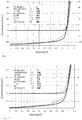
- Fig. 1 shows the result of grazing incidence X-ray diffraction (GIXRD) of a 5 nm thick polyphenol-containing layer. The layers were vacuum deposited on a 10nm C60 coated Si wafer.
- GIXRD grazing incidence X-ray diffraction
- Fig. 1 The deposition of in Fig. 1
- the template used as a template was at room temperature of the substrate.
- the three Bragg reflections at 2 ⁇ of 10.9 °, 18.2 °, and 20.7 ° are assigned to the cubic face centered phase (fcc) of the C60 sublayer [ Elschner, C. et al .: Determining the C60 molecular arrangement in thin films by means of X-ray diffraction. Journal of Applied Crystallography, 44 (5): 983-990, 2011 ].
- the reflection at 27.6 ° is assigned to the template layer and indicates that this nanocrystal grows in pi-pi stacks on C60.
- the distance between the crystal planes is 3.23 ⁇ .
- the template molecules are aligned parallel to the substrate, the pi-pi stacking direction is perpendicular to the substrate.
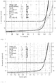
- Fig. 2 are the results of GIXRD measurements on a 30 nm donor: C60 mixed layer, using the ADA oligomer DCV4T-Et2, cf. Fig. 10 as a donor, deposited on a 10 nm C60 / Si substrate with and without a 5 nm template layer.
- the donor: C60 mixed layer was deposited at a substrate temperature of 40 ° C, the mixing ratio is 2: 1 mass%. This mixed layer grows on C60 nanocrystalline.
- the X-ray diffractogram of the mixed layer grown on the template layer shows the characteristic of the templating molecule ellagic acid reflex at 27.6 ° (see FIG. Fig. 1 ).
- the crystal plane distance for the reflex at 26.1 ° corresponds to 3.4 ⁇ , indicating a face-on growth or at least a strong one Substrate tilted orientation of the donor molecules.
- the mean size of the donor crystallites was evaluated using the Scherrer equation and is 8.1 nm.
- the measurement results prove that the orientation of the donor molecules was affected by the template layer and the crystallinity of the donor phase in the mixed layer was improved.
- the thin template layer changes orientation from standing to face-on and enhancing the crystallinity of the ZnPc molecules.
- Fig. 4 presents results of GIXRD measurements on donor: C60 mixed layers, with DCV5T-Me2 (3,3) as donor, deposited on 10 nm C60 with and without template layer.
- the 30 nm thick mixed layers were deposited on 80 ° C heated substrate, the mixing ratio is 2: 1.
- the X-ray diffraction pattern shows the characteristic peaks of the C60 fcc phase for both donor: C60 mixed layers.
- the donor in the mixed layer, deposited directly on C60 grows amorphous.
- reflections in the 2 ⁇ region between 24 ° and 30 ° appear on the template layer. These are assigned to the donor phase in the mixed layer and the template layer. Accordingly, the donor on the template layer grows crystalline.
- the reflections between 24 ° and 30 ° correspond to Bragg distances of 3.7 ⁇ and 3.4 ⁇ .
- the photoactive layer has a thickness of 30 nm.
- the deposition of the photoactive layer was carried out at a substrate temperature of 40 ° C.
- the mixing ratio between donor and C60 is 2: 1.
- the gray curve shows the current-voltage characteristic of a device in which the photoactive layer was deposited directly on C60 and the black curve shows the current-voltage characteristic of a photoactive layer device deposited on a 5 nm thick template layer.
- an increase of the fill factor by 13.6% is observed (from 45.2% to 58.8%). This is in accordance with the results of the GIXRD measurement ( Fig. 2 ) due to the improved crystallinity of the photoactive layer.
- the template layer thus leads to a significantly improved solar cell.
- Fig. 6 shows the measurement results of two solar cells with a photoactive layer of donor: C60 (DCV4T-Et2: C60).
- the photoactive layer has a thickness of 30 nm. Their deposition was carried out at a substrate temperature of 70 ° C.
- the gray characteristic shows the current-voltage characteristic of the device where the donor: C60 layer is deposited directly on C60 and the black characteristic shows the current-voltage characteristic of a device with donor: C60 layer deposited on a 5nm thick template layer.
- the fill factor of the solar cell with the template layer is 55.7%, compared to the solar cell without templating layer has a lower fill factor of 44.9%.
- Fig. 7 shows the measurement results of two solar cells containing ZnPc: C60 as the photoactive layer.
- the photoactive layer has a thickness of 30 nm. Their deposition was carried out at a substrate temperature of 70 ° C.
- the gray curve represents the current-voltage characteristic of the device in which the ZnPc: C60 layer was deposited directly on C60, whereas the black curve shows the current-voltage characteristic of a device with ZnPc: C60 layer deposited on a 5 nm thick template layer
- the solar cell without template layer has a fill factor of 36.1%, in contrast, the cell with template layer has a significantly better fill factor of 55.3%.
- the improved fill factor is due to the crystallinity of the ZnPc phase in the mixed layer caused by the template layer.
- the photoactive layer has a thickness of 30 nm.
- the deposition of the photoactive layer was carried out at a substrate temperature of 70 ° C.
- the mixing ratio between donor and C60 is 2: 1.
- the gray curve in Fig. 8 show the Current-voltage characteristic of a device in which the photoactive layer was deposited directly on C60, and the black curve, the current-voltage characteristic of a device with a photoactive layer deposited on a 2 nm thick template layer.
- Fig. 9 shows as a surprising finding the results of the lifetime measurements of bulk heterojunction solar cells after 800 hours of accelerated aging in the oven at 85 ° C.
- the donor: C60 mixed layer was deposited directly on the intrinsic C60 layer or on a template layer.
- the measurement results indicate a stabilizing effect of the template layer on the life of the solar cells.
- One possible explanation is the formation of a more stable fill factor by the preferred molecular orientation achieved with the template material.
Priority Applications (6)
| Application Number | Priority Date | Filing Date | Title |
|---|---|---|---|
| EP17173859.4A EP3410505A1 (fr) | 2017-05-31 | 2017-05-31 | Polyphénole et dérivés de polyamino dans des éléments constitutifs optoélectroniques organiques |
| PCT/EP2018/064391 WO2018220148A1 (fr) | 2017-05-31 | 2018-05-31 | Polyphénols et dérivés polyamino dans des composants optoélectroniques organiques |
| CN201880049474.1A CN110945676B (zh) | 2017-05-31 | 2018-05-31 | 有机光电子部件中的多酚和多氨基衍生物 |
| US16/618,482 US20200381627A1 (en) | 2017-05-31 | 2018-05-31 | Polyphenols and polyamino derivatives in organic optoelectronic components |
| KR1020197038716A KR102361584B1 (ko) | 2017-05-31 | 2018-05-31 | 유기 광전자 컴포넌트의 폴리페놀 및 폴리아미노 유도체 |
| EP18730992.7A EP3631873A1 (fr) | 2017-05-31 | 2018-05-31 | Polyphénols et dérivés polyamino dans des composants optoélectroniques organiques |
Applications Claiming Priority (1)
| Application Number | Priority Date | Filing Date | Title |
|---|---|---|---|
| EP17173859.4A EP3410505A1 (fr) | 2017-05-31 | 2017-05-31 | Polyphénole et dérivés de polyamino dans des éléments constitutifs optoélectroniques organiques |
Publications (1)
| Publication Number | Publication Date |
|---|---|
| EP3410505A1 true EP3410505A1 (fr) | 2018-12-05 |
Family
ID=59021294
Family Applications (2)
| Application Number | Title | Priority Date | Filing Date |
|---|---|---|---|
| EP17173859.4A Withdrawn EP3410505A1 (fr) | 2017-05-31 | 2017-05-31 | Polyphénole et dérivés de polyamino dans des éléments constitutifs optoélectroniques organiques |
| EP18730992.7A Pending EP3631873A1 (fr) | 2017-05-31 | 2018-05-31 | Polyphénols et dérivés polyamino dans des composants optoélectroniques organiques |
Family Applications After (1)
| Application Number | Title | Priority Date | Filing Date |
|---|---|---|---|
| EP18730992.7A Pending EP3631873A1 (fr) | 2017-05-31 | 2018-05-31 | Polyphénols et dérivés polyamino dans des composants optoélectroniques organiques |
Country Status (5)
| Country | Link |
|---|---|
| US (1) | US20200381627A1 (fr) |
| EP (2) | EP3410505A1 (fr) |
| KR (1) | KR102361584B1 (fr) |
| CN (1) | CN110945676B (fr) |
| WO (1) | WO2018220148A1 (fr) |
Citations (8)
| Publication number | Priority date | Publication date | Assignee | Title |
|---|---|---|---|---|
| US20020098346A1 (en) | 1998-03-27 | 2002-07-25 | Yissum Research Development Company Of The Hebrew University Of Jerusalem | Molecular layer epitaxy method and compositions |
| WO2004083958A2 (fr) | 2003-03-19 | 2004-09-30 | Technische Universität Dresden | Composant photo-actif presentant des couches organiques |
| WO2006092134A1 (fr) | 2005-03-04 | 2006-09-08 | Heliatek Gmbh | Composant photoactif organique |
| WO2010044122A1 (fr) * | 2008-10-16 | 2010-04-22 | Giuseppe Calogero | Cellule solaire photoélectrochimique comprenant des teintures d'activation d'anthocyane et de bétalaïne d'origine végétale ou synthétique ou mélanges de celles-ci |
| WO2011025567A2 (fr) | 2009-06-03 | 2011-03-03 | The Regents Of The University Of Michigan | Gabarit structurel pour dispositifs électroniques organiques possédant un film organique avec ordre à longue distance |
| WO2011138021A2 (fr) | 2010-05-04 | 2011-11-10 | Heliatek Gmbh | Composant photoactif à couches organiques |
| WO2011161262A1 (fr) | 2010-06-24 | 2011-12-29 | Heliatek Gmbh | Matériau organique semi-conducteur évaporable et son utilisation dans un composant opto-électronique |
| WO2014128277A1 (fr) | 2013-02-21 | 2014-08-28 | Heliatek | Matériau organique, photo-actif pour composants optoélectroniques |
Family Cites Families (4)
| Publication number | Priority date | Publication date | Assignee | Title |
|---|---|---|---|---|
| US20050224905A1 (en) * | 2004-04-13 | 2005-10-13 | Forrest Stephen R | High efficiency organic photovoltaic cells employing hybridized mixed-planar heterojunctions |
| US8067763B2 (en) * | 2007-12-19 | 2011-11-29 | Honeywell International Inc. | Quantum dot solar cell with conjugated bridge molecule |
| US20120216870A1 (en) * | 2009-11-03 | 2012-08-30 | University Of Florida Research Foundation Inc. | Interlayer for organic solar cells |
| KR20150137730A (ko) * | 2014-05-30 | 2015-12-09 | 재단법인 녹색에너지연구원 | 염료감응 태양전지용 천연 염료 제조방법 |
-
2017
- 2017-05-31 EP EP17173859.4A patent/EP3410505A1/fr not_active Withdrawn
-
2018
- 2018-05-31 CN CN201880049474.1A patent/CN110945676B/zh active Active
- 2018-05-31 WO PCT/EP2018/064391 patent/WO2018220148A1/fr active Application Filing
- 2018-05-31 KR KR1020197038716A patent/KR102361584B1/ko active IP Right Grant
- 2018-05-31 US US16/618,482 patent/US20200381627A1/en active Pending
- 2018-05-31 EP EP18730992.7A patent/EP3631873A1/fr active Pending
Patent Citations (8)
| Publication number | Priority date | Publication date | Assignee | Title |
|---|---|---|---|---|
| US20020098346A1 (en) | 1998-03-27 | 2002-07-25 | Yissum Research Development Company Of The Hebrew University Of Jerusalem | Molecular layer epitaxy method and compositions |
| WO2004083958A2 (fr) | 2003-03-19 | 2004-09-30 | Technische Universität Dresden | Composant photo-actif presentant des couches organiques |
| WO2006092134A1 (fr) | 2005-03-04 | 2006-09-08 | Heliatek Gmbh | Composant photoactif organique |
| WO2010044122A1 (fr) * | 2008-10-16 | 2010-04-22 | Giuseppe Calogero | Cellule solaire photoélectrochimique comprenant des teintures d'activation d'anthocyane et de bétalaïne d'origine végétale ou synthétique ou mélanges de celles-ci |
| WO2011025567A2 (fr) | 2009-06-03 | 2011-03-03 | The Regents Of The University Of Michigan | Gabarit structurel pour dispositifs électroniques organiques possédant un film organique avec ordre à longue distance |
| WO2011138021A2 (fr) | 2010-05-04 | 2011-11-10 | Heliatek Gmbh | Composant photoactif à couches organiques |
| WO2011161262A1 (fr) | 2010-06-24 | 2011-12-29 | Heliatek Gmbh | Matériau organique semi-conducteur évaporable et son utilisation dans un composant opto-électronique |
| WO2014128277A1 (fr) | 2013-02-21 | 2014-08-28 | Heliatek | Matériau organique, photo-actif pour composants optoélectroniques |
Non-Patent Citations (6)
| Title |
|---|
| ELSCHNER, C. U.A.: "Determining the C60 molecular arrangement in thin films by means of X-ray diffraction", JOURNAL OF APPLIED CRYSTALLOGRAPHY, vol. 44, no. 5, 2011, pages 983 - 990 |
| GUSKOVA, 0.: "Light absorption in organic solar cells: The importance of oriented molecules", J. PHYS. CHEM. C, vol. 117, no. 33, 2013, pages 17285 - 17293 |
| KUMARA G R A ET AL: "Shiso leaf pigments for dye-sensitized solid-state solar cell", SOLAR ENERGY MATERIALS AND SOLAR CELLS, ELSEVIER SCIENCE PUBLISHERS, AMSTERDAM, NL, vol. 90, no. 9, 23 May 2006 (2006-05-23), pages 1220 - 1226, XP028002186, ISSN: 0927-0248, [retrieved on 20060523], DOI: 10.1016/J.SOLMAT.2005.07.007 * |
| LAILY A R N ET AL: "Poly (3-Dodecylthiophene)/Natural Dye Bulk Heterojunction Organic Solar Cell: An Electrical Conductivity, and Hall Effect Study", PROCEDIA CHEMISTRY, ELSEVIER, AMSTERDAM, NL, vol. 19, 24 March 2016 (2016-03-24), pages 2 - 9, XP029471411, ISSN: 1876-6196, DOI: 10.1016/J.PROCHE.2016.03.003 * |
| RAMAMOORTHY RAJA ET AL: "Betalain and anthocyanin dye-sensitized solar cells", JOURNAL OF APPLIED ELECTROCHEMISTRY, SPRINGER, DORDRECHT, NL, vol. 46, no. 9, 4 June 2016 (2016-06-04), pages 929 - 941, XP036025416, ISSN: 0021-891X, [retrieved on 20160604], DOI: 10.1007/S10800-016-0974-9 * |
| THE JOURNAL OF PHYSICAL CHEMISTRY C, vol. 117, 2013, pages 11600 - 11609 |
Also Published As
| Publication number | Publication date |
|---|---|
| CN110945676A (zh) | 2020-03-31 |
| CN110945676B (zh) | 2024-04-16 |
| EP3631873A1 (fr) | 2020-04-08 |
| US20200381627A1 (en) | 2020-12-03 |
| KR102361584B1 (ko) | 2022-02-09 |
| KR20200014841A (ko) | 2020-02-11 |
| WO2018220148A1 (fr) | 2018-12-06 |
Similar Documents
| Publication | Publication Date | Title |
|---|---|---|
| EP1861886B8 (fr) | Composant photoactif organique | |
| DE102009051142B4 (de) | Photoaktives Bauelement mit invertierter Schichtfolge und Verfahren zu seiner Herstellung | |
| EP1859494A1 (fr) | Composant photoactif a couches organiques | |
| EP2329539A1 (fr) | Utilisation du dibenzotetraphenylperiflanthene dans des cellules solaires organiques | |
| DE102013106639A1 (de) | Organisches, halbleitendes Bauelement | |
| WO2011161170A1 (fr) | Composant optoélectronique comportant des couches organiques | |
| EP2867932B1 (fr) | Électrode transparente pour composants optoélectroniques | |
| DE102009038633B4 (de) | Photoaktives Bauelement mit organischen Doppel- bzw. Mehrfachmischschichten | |
| DE112020007073T5 (de) | Verarbeitung von effizienten perovskit-solarzellen in feuchter luft basierend auf polymerisierbaren ionischen flüssigkeiten und salzen | |
| DE102015101768A1 (de) | Lichtabsorber | |
| DE102009036110A1 (de) | Licht absorbierendes organisches Bauelement | |
| EP3410505A1 (fr) | Polyphénole et dérivés de polyamino dans des éléments constitutifs optoélectroniques organiques | |
| EP4256632A1 (fr) | Système stratifié pour composant électronique organique | |
| WO2021058065A1 (fr) | Composés possédant un groupe furopyrolle ou un groupe thiénopyrolle, composant optoélectronique comprenant ce type de composé, et utilisation de ce type de composé dans des composants optoélectroniques | |
| DE102012105810B4 (de) | Transparente Elektrode für optoelektronische Bauelemente | |
| EP4147283A1 (fr) | Système laser pour composant électronique organique | |
| DE102021130501A1 (de) | Schichtsystem mit mindestens einer photoaktiven Schicht mit mindestens einer Zwischenschicht für ein organisches elektronisches Bauelement | |
| WO2021018351A1 (fr) | Composé semiconducteur organique avec un groupe indol, composant optoélectronique organique comprenant ledit composé et utilisation dudit composé | |
| DE102019118872A1 (de) | Organische Verbindung, und optoelektronisches Bauelement mit einer solchen organischen Verbindung | |
| WO2024002432A1 (fr) | Composant optoélectronique avec une couche photoactive réalisée sous la forme d'une hétérojonction plane | |
| DE102013110373A1 (de) | Optoelektronisches Bauelement | |
| DE102007037906A1 (de) | Elektronisches Bauelement und Verwendung von stickstoffhaltigen Makrozyklen als Dielektrikum in organischen elektronischen Bauteilen |
Legal Events
| Date | Code | Title | Description |
|---|---|---|---|
| PUAI | Public reference made under article 153(3) epc to a published international application that has entered the european phase |
Free format text: ORIGINAL CODE: 0009012 |
|
| AK | Designated contracting states |
Kind code of ref document: A1 Designated state(s): AL AT BE BG CH CY CZ DE DK EE ES FI FR GB GR HR HU IE IS IT LI LT LU LV MC MK MT NL NO PL PT RO RS SE SI SK SM TR |
|
| AX | Request for extension of the european patent |
Extension state: BA ME |
|
| STAA | Information on the status of an ep patent application or granted ep patent |
Free format text: STATUS: THE APPLICATION IS DEEMED TO BE WITHDRAWN |
|
| 18D | Application deemed to be withdrawn |
Effective date: 20190606 |