EP3410499A1 - Light emitting device, and manufacturing method of light emitting device - Google Patents
Light emitting device, and manufacturing method of light emitting device Download PDFInfo
- Publication number
- EP3410499A1 EP3410499A1 EP16888128.2A EP16888128A EP3410499A1 EP 3410499 A1 EP3410499 A1 EP 3410499A1 EP 16888128 A EP16888128 A EP 16888128A EP 3410499 A1 EP3410499 A1 EP 3410499A1
- Authority
- EP
- European Patent Office
- Prior art keywords
- light emitting
- emitting device
- molded body
- resin molded
- led elements
- Prior art date
- Legal status (The legal status is an assumption and is not a legal conclusion. Google has not performed a legal analysis and makes no representation as to the accuracy of the status listed.)
- Granted
Links
Images


Classifications
-
- H—ELECTRICITY
- H10—SEMICONDUCTOR DEVICES; ELECTRIC SOLID-STATE DEVICES NOT OTHERWISE PROVIDED FOR
- H10H—INORGANIC LIGHT-EMITTING SEMICONDUCTOR DEVICES HAVING POTENTIAL BARRIERS
- H10H20/00—Individual inorganic light-emitting semiconductor devices having potential barriers, e.g. light-emitting diodes [LED]
- H10H20/80—Constructional details
- H10H20/85—Packages
- H10H20/852—Encapsulations
- H10H20/854—Encapsulations characterised by their material, e.g. epoxy or silicone resins
-
- B—PERFORMING OPERATIONS; TRANSPORTING
- B29—WORKING OF PLASTICS; WORKING OF SUBSTANCES IN A PLASTIC STATE IN GENERAL
- B29C—SHAPING OR JOINING OF PLASTICS; SHAPING OF MATERIAL IN A PLASTIC STATE, NOT OTHERWISE PROVIDED FOR; AFTER-TREATMENT OF THE SHAPED PRODUCTS, e.g. REPAIRING
- B29C45/00—Injection moulding, i.e. forcing the required volume of moulding material through a nozzle into a closed mould; Apparatus therefor
- B29C45/14—Injection moulding, i.e. forcing the required volume of moulding material through a nozzle into a closed mould; Apparatus therefor incorporating preformed parts or layers, e.g. injection moulding around inserts or for coating articles
-
- B—PERFORMING OPERATIONS; TRANSPORTING
- B29—WORKING OF PLASTICS; WORKING OF SUBSTANCES IN A PLASTIC STATE IN GENERAL
- B29C—SHAPING OR JOINING OF PLASTICS; SHAPING OF MATERIAL IN A PLASTIC STATE, NOT OTHERWISE PROVIDED FOR; AFTER-TREATMENT OF THE SHAPED PRODUCTS, e.g. REPAIRING
- B29C45/00—Injection moulding, i.e. forcing the required volume of moulding material through a nozzle into a closed mould; Apparatus therefor
- B29C45/14—Injection moulding, i.e. forcing the required volume of moulding material through a nozzle into a closed mould; Apparatus therefor incorporating preformed parts or layers, e.g. injection moulding around inserts or for coating articles
- B29C45/14639—Injection moulding, i.e. forcing the required volume of moulding material through a nozzle into a closed mould; Apparatus therefor incorporating preformed parts or layers, e.g. injection moulding around inserts or for coating articles for obtaining an insulating effect, e.g. for electrical components
-
- H—ELECTRICITY
- H10—SEMICONDUCTOR DEVICES; ELECTRIC SOLID-STATE DEVICES NOT OTHERWISE PROVIDED FOR
- H10P—GENERIC PROCESSES OR APPARATUS FOR THE MANUFACTURE OR TREATMENT OF DEVICES COVERED BY CLASS H10
- H10P72/00—Handling or holding of wafers, substrates or devices during manufacture or treatment thereof
- H10P72/70—Handling or holding of wafers, substrates or devices during manufacture or treatment thereof for supporting or gripping
- H10P72/74—Handling or holding of wafers, substrates or devices during manufacture or treatment thereof for supporting or gripping using temporarily an auxiliary support
- H10P72/7402—Wafer tapes, e.g. grinding or dicing support tapes
-
- H—ELECTRICITY
- H10—SEMICONDUCTOR DEVICES; ELECTRIC SOLID-STATE DEVICES NOT OTHERWISE PROVIDED FOR
- H10W—GENERIC PACKAGES, INTERCONNECTIONS, CONNECTORS OR OTHER CONSTRUCTIONAL DETAILS OF DEVICES COVERED BY CLASS H10
- H10W90/00—Package configurations
-
- H—ELECTRICITY
- H10—SEMICONDUCTOR DEVICES; ELECTRIC SOLID-STATE DEVICES NOT OTHERWISE PROVIDED FOR
- H10H—INORGANIC LIGHT-EMITTING SEMICONDUCTOR DEVICES HAVING POTENTIAL BARRIERS
- H10H20/00—Individual inorganic light-emitting semiconductor devices having potential barriers, e.g. light-emitting diodes [LED]
- H10H20/01—Manufacture or treatment
- H10H20/036—Manufacture or treatment of packages
-
- H—ELECTRICITY
- H10—SEMICONDUCTOR DEVICES; ELECTRIC SOLID-STATE DEVICES NOT OTHERWISE PROVIDED FOR
- H10H—INORGANIC LIGHT-EMITTING SEMICONDUCTOR DEVICES HAVING POTENTIAL BARRIERS
- H10H20/00—Individual inorganic light-emitting semiconductor devices having potential barriers, e.g. light-emitting diodes [LED]
- H10H20/01—Manufacture or treatment
- H10H20/036—Manufacture or treatment of packages
- H10H20/0362—Manufacture or treatment of packages of encapsulations
-
- H—ELECTRICITY
- H10—SEMICONDUCTOR DEVICES; ELECTRIC SOLID-STATE DEVICES NOT OTHERWISE PROVIDED FOR
- H10H—INORGANIC LIGHT-EMITTING SEMICONDUCTOR DEVICES HAVING POTENTIAL BARRIERS
- H10H20/00—Individual inorganic light-emitting semiconductor devices having potential barriers, e.g. light-emitting diodes [LED]
- H10H20/01—Manufacture or treatment
- H10H20/036—Manufacture or treatment of packages
- H10H20/0364—Manufacture or treatment of packages of interconnections
-
- H—ELECTRICITY
- H10—SEMICONDUCTOR DEVICES; ELECTRIC SOLID-STATE DEVICES NOT OTHERWISE PROVIDED FOR
- H10H—INORGANIC LIGHT-EMITTING SEMICONDUCTOR DEVICES HAVING POTENTIAL BARRIERS
- H10H20/00—Individual inorganic light-emitting semiconductor devices having potential barriers, e.g. light-emitting diodes [LED]
- H10H20/80—Constructional details
- H10H20/83—Electrodes
-
- H—ELECTRICITY
- H10—SEMICONDUCTOR DEVICES; ELECTRIC SOLID-STATE DEVICES NOT OTHERWISE PROVIDED FOR
- H10H—INORGANIC LIGHT-EMITTING SEMICONDUCTOR DEVICES HAVING POTENTIAL BARRIERS
- H10H20/00—Individual inorganic light-emitting semiconductor devices having potential barriers, e.g. light-emitting diodes [LED]
- H10H20/80—Constructional details
- H10H20/85—Packages
- H10H20/857—Interconnections, e.g. lead-frames, bond wires or solder balls
-
- H—ELECTRICITY
- H10—SEMICONDUCTOR DEVICES; ELECTRIC SOLID-STATE DEVICES NOT OTHERWISE PROVIDED FOR
- H10H—INORGANIC LIGHT-EMITTING SEMICONDUCTOR DEVICES HAVING POTENTIAL BARRIERS
- H10H20/00—Individual inorganic light-emitting semiconductor devices having potential barriers, e.g. light-emitting diodes [LED]
- H10H20/80—Constructional details
- H10H20/85—Packages
- H10H20/858—Means for heat extraction or cooling
- H10H20/8581—Means for heat extraction or cooling characterised by their material
-
- H—ELECTRICITY
- H10—SEMICONDUCTOR DEVICES; ELECTRIC SOLID-STATE DEVICES NOT OTHERWISE PROVIDED FOR
- H10P—GENERIC PROCESSES OR APPARATUS FOR THE MANUFACTURE OR TREATMENT OF DEVICES COVERED BY CLASS H10
- H10P72/00—Handling or holding of wafers, substrates or devices during manufacture or treatment thereof
- H10P72/70—Handling or holding of wafers, substrates or devices during manufacture or treatment thereof for supporting or gripping
- H10P72/74—Handling or holding of wafers, substrates or devices during manufacture or treatment thereof for supporting or gripping using temporarily an auxiliary support
- H10P72/744—Details of chemical or physical process used for separating the auxiliary support from a device or a wafer
- H10P72/7442—Separation by peeling
-
- H—ELECTRICITY
- H10—SEMICONDUCTOR DEVICES; ELECTRIC SOLID-STATE DEVICES NOT OTHERWISE PROVIDED FOR
- H10W—GENERIC PACKAGES, INTERCONNECTIONS, CONNECTORS OR OTHER CONSTRUCTIONAL DETAILS OF DEVICES COVERED BY CLASS H10
- H10W72/00—Interconnections or connectors in packages
- H10W72/01—Manufacture or treatment
- H10W72/0198—Manufacture or treatment batch processes
-
- H—ELECTRICITY
- H10—SEMICONDUCTOR DEVICES; ELECTRIC SOLID-STATE DEVICES NOT OTHERWISE PROVIDED FOR
- H10W—GENERIC PACKAGES, INTERCONNECTIONS, CONNECTORS OR OTHER CONSTRUCTIONAL DETAILS OF DEVICES COVERED BY CLASS H10
- H10W72/00—Interconnections or connectors in packages
- H10W72/90—Bond pads, in general
- H10W72/941—Dispositions of bond pads
- H10W72/9413—Dispositions of bond pads on encapsulations
-
- H—ELECTRICITY
- H10—SEMICONDUCTOR DEVICES; ELECTRIC SOLID-STATE DEVICES NOT OTHERWISE PROVIDED FOR
- H10W—GENERIC PACKAGES, INTERCONNECTIONS, CONNECTORS OR OTHER CONSTRUCTIONAL DETAILS OF DEVICES COVERED BY CLASS H10
- H10W74/00—Encapsulations, e.g. protective coatings
- H10W74/01—Manufacture or treatment
- H10W74/019—Manufacture or treatment using temporary auxiliary substrates
-
- H—ELECTRICITY
- H10—SEMICONDUCTOR DEVICES; ELECTRIC SOLID-STATE DEVICES NOT OTHERWISE PROVIDED FOR
- H10W—GENERIC PACKAGES, INTERCONNECTIONS, CONNECTORS OR OTHER CONSTRUCTIONAL DETAILS OF DEVICES COVERED BY CLASS H10
- H10W74/00—Encapsulations, e.g. protective coatings
- H10W74/10—Encapsulations, e.g. protective coatings characterised by their shape or disposition
- H10W74/131—Encapsulations, e.g. protective coatings characterised by their shape or disposition the semiconductor body being only partially enclosed
- H10W74/142—Encapsulations, e.g. protective coatings characterised by their shape or disposition the semiconductor body being only partially enclosed the encapsulations exposing the passive side of the semiconductor body
-
- H—ELECTRICITY
- H10—SEMICONDUCTOR DEVICES; ELECTRIC SOLID-STATE DEVICES NOT OTHERWISE PROVIDED FOR
- H10W—GENERIC PACKAGES, INTERCONNECTIONS, CONNECTORS OR OTHER CONSTRUCTIONAL DETAILS OF DEVICES COVERED BY CLASS H10
- H10W90/00—Package configurations
- H10W90/10—Configurations of laterally-adjacent chips
Definitions
- miniaturization of light emitting devices is required.
- the light emitting device 101 obtained by a mounting method using the conventional solder material 122 it is necessary to secure a space for installing the solder material 122 in the light emitting device 101 from a viewpoint of wet-spreading of the solder material 122 or ensuring mounting strength. Therefore, the miniaturization of the light emitting device 101 is limited.
- Patent Literature 2 discloses a method of fixing a mounting position of an LED by applying an adhesive in a hole formed in a printed circuit board, mounting an LED on the adhesive, and curing it.
- Embodiment 1 according to the present invention will be described below with reference to Figs. 1 to 3 .
- the LED elements 3 to 6 are surface mounted device (SMD) type LED elements. As illustrated in Fig. 1 , the LED element 3 includes a base portion 31, a light emitting unit 32, an anode 33 (electrode), and a cathode 34 (electrode).
- the LED element 4 includes a base portion 41, a light emitting unit 42, an anode 43 (electrode), and a cathode 44 (electrode).
- the LED element 5 includes a base portion 51, a light emitting unit 52, an anode 53 (electrode), and a cathode 54 (electrode).
- the LED element 6 includes a base portion 61, a light emitting unit 62, an anode 63 (electrode), and a cathode 64 (electrode).
- interconnections 71 to 75 can be fabricated by various methods.
- a method of print-forming the interconnections 71 to 75 by jetting a conductive material (for example, silver ink or the like) using an ink jet printer or the like, a method of forming the interconnections 71 to 75 using an aerosol, a method of forming the interconnections 71 to 75 using a dispenser, or the like can be exemplified.
- the light emitting device 1 illustrated in Fig. 1 does not have a printed circuit board which is necessary for a light emitting device according to a conventional technology and also does not need a solder material for connecting interconnections and electrodes (an anode and a cathode). Thereby, the following effects which contribute to miniaturization and thinning of the light emitting device 1 can be obtained.
- Embodiment 3 according to the present invention will be described below.
- members having the same functions as those described in the above embodiment will be denoted by the same reference signs, and description thereof will be omitted.
- each LED element 103 leaks, for example, also toward adjacent LED elements 103 in addition to an upper direction indicated by arrows in Fig. 6 . Thereby, light emission from each LED element 103 interferes with each other.
- the light emitting device 101 in such a state is used for an optical printer head or the like, such a problem in which a dot image is blurred or written and stored image qualities are deteriorated occurs.
- a material having thermal conductivity of 1 W1m ⁇ K or higher is used as the material of the resin molded body 2.
- a material having thermal conductivity of 1 W1m ⁇ K or higher is used as the material of the resin molded body 2.
- a nylon-based resin mixed with TORELINA H718LB (manufactured by Toray Industries, Inc.) or high thermal conductive insulating filler manufactured by Unitika Ltd. can be exemplified.
- the interconnections 91 to 95 are interconnections connected to the connection electrodes of the electronic parts 81 to 83 and are formed on the back surface 23 of the resin molded body 2 by a printing method using silver ink or the like as in the interconnections 71 and 72. Therefore, a soldering material for connecting the connection electrodes of the electronic parts 81 to 83 and the interconnections 91 to 95 is unnecessary.
- a light emitting device includes a resin molded body, a light emitting element having at least a light emitting unit and an electrode and embedded in the resin molded body so that the light emitting unit faces a front surface of the resin molded body and the electrode is exposed on a back surface opposite to the front surface of the resin molded body, and an interconnection formed on the back surface of the resin molded body and connected to the electrode.
- the light emitting element is mounted on the light emitting device in a form of being embedded in the resin molded body. Therefore, since a printed circuit board for mounting the light emitting element is not required, a height of the light emitting device can be made substantially the same as a height of the light emitting element (resin molded body).
- the interconnection connected to the electrode of the light emitting element exposed on the back surface of the resin molded body can be formed by printing, there is no need to use a solder material for connection. Thereby, since spaces for the solder material between the light emitting elements are unnecessary, mounting pitches between the light emitting elements can be minimized.
- the light emitting device is further characterized in that the light emitting unit is exposed on the front surface.
- the resin molded body can be formed of a material having a low light transmittance.
- the light emitting device is further characterized in that an optical part which imparts directivity to light from the light emitting unit is formed on an upper portion of the light emitting unit of the resin molded body.
- the light emitting device is further characterized in that the light emitting element is a light emitting diode element.
Landscapes
- Engineering & Computer Science (AREA)
- Manufacturing & Machinery (AREA)
- Mechanical Engineering (AREA)
- Led Device Packages (AREA)
- Illuminated Signs And Luminous Advertising (AREA)
- Injection Moulding Of Plastics Or The Like (AREA)
Abstract
Description
- The present invention relates to a light emitting device having a light emitting element such as a light emitting diode (LED) element.
- Conventionally, a light emitting device having a plurality of light emitting diode (LED) elements is often used as an optical printer head used in a printer of an electrophotographic-type or the like, or a light emitting electronic device used in an optical display device or the like. An example of such a light emitting device is illustrated in
Fig. 6 . -
Fig. 6 is a diagram illustrating a configuration of alight emitting device 101 according to a conventional technology. As illustrated inFig. 6(a) , thelight emitting device 101 includes aprinted circuit board 102 and a plurality ofLED elements 103. As illustrated inFig. 6(b) , theLED element 103 includes abase portion 131, alight emitting unit 132, ananode 133, and acathode 134. - On a surface of the printed
circuit board 102, aninterconnection 121 is formed by a method such as etching. - The
light emitting unit 132 formed of a light emitting diode is provided on one surface of thebase portion 131. Further, theanode 133 and thecathode 134 are provided on the other surface of thebase portion 131. Each of theLED elements 103 is mounted on the surface of the printedcircuit board 102 by connecting theanode 133 and thecathode 134 to theinterconnection 121 using asolder material 122. - However, in the configuration in which the
LED element 103 is mounted on the surface of the printedcircuit board 102 as in thelight emitting device 101 illustrated inFig. 6 , due to thermal contraction or the like of thesolder material 122 when thesolder material 122 is cured, there is a possibility of a height and a mounting position of theLED element 103 deviating from specifications. When such deviation occurs, a problem in which light emission characteristics of the completedlight emitting device 101 deviate from the specifications occurs. Further, there is also a problem in which characteristics of theLED element 103 are changed due to application of high temperature heat for curing thesolder material 122. - Further, due to an increasing demand for miniaturization and thinning of electronic devices in recent years, miniaturization of light emitting devices is required. However, in the
light emitting device 101 obtained by a mounting method using theconventional solder material 122, it is necessary to secure a space for installing thesolder material 122 in thelight emitting device 101 from a viewpoint of wet-spreading of thesolder material 122 or ensuring mounting strength. Therefore, the miniaturization of thelight emitting device 101 is limited. - Thus, conventionally, various countermeasures against such deviation of the LED position at the time of surface mounting with the solder material have been proposed.
-
Patent Literature 1 discloses a method of fixing a mounting position of an LED by forming a groove at an LED mounting position on a printed circuit board and inserting an LED member joined with a dummy having the same dimension as a mounting pitch of the LED into the groove. -
Patent Literature 2 discloses a method of fixing a mounting position of an LED by applying an adhesive in a hole formed in a printed circuit board, mounting an LED on the adhesive, and curing it. -
Patent Literature 3 discloses a method of fixing a mounting position of an LED by assembling an LED with a member whose positioning has been performed once and then soldering the LED to a circuit of a printed circuit board. -
- [Patent Literature 1] Japanese Unexamined Patent Application Publication No.
S64-25582 (Publication date: January 27, 1989 - [Patent Literature 2] Japanese Unexamined Patent Application Publication No.
H11-219961 (Publication date: August 10, 1999 - [Patent Literature 3] Japanese Unexamined Patent Application Publication No.
2008-16297 (Publication date: January 24, 2008 - [Patent Literature 4] Japanese Unexamined Patent Application Publication No.
H05-150807 (Publication date: July 30, 1993 - [Patent Literature 5] Japanese Unexamined Patent Application Publication No.
H09-179512 (Publication date: July 11, 1997 - However, in these conventional technologies, it is difficult to realize accuracy of an LED mounting position in micron units from a viewpoint of the processing accuracy of substrate processing, a dummy member, an assembling member, and the like. Also, there is a problem in that processing spaces for grooves or holes, or installation spaces for dummy members or assembling members are required, thereby increasing a size of the light emitting device. Further, there are additional problems in that additional processing is applied to the printed circuit board, manufacturing cost is increased for fabrication of assembling members, and manufacturing yield is lowered due to complicated manufacturing steps.
- The present invention has been made to solve the problems described above. The object is to realize a more compact and thinner light emitting device, and a method for more easily manufacturing such a light emitting device.
- In order to solve the above problems, a light emitting device according to one aspect of the present invention includes a resin molded body, a light emitting element having at least a light emitting unit and an electrode and that is embedded in the resin molded body so that the light emitting unit faces a front surface of the resin molded body and the electrode is exposed on a back surface opposite to the front surface of the resin molded body, and an interconnection formed on the back surface of the resin molded body and connected to the electrode.
- In order to solve the above problems, a method of manufacturing a light emitting device according to one aspect of the present invention includes a step of temporarily fixing a light emitting element having at least a light emitting unit and an electrode on a temporary fixing film in a form in which the electrode comes into contact with the temporary fixing film, a step of forming a resin molded body in which the light emitting element is embedded by disposing the temporary fixing film to which the light emitting element is temporarily fixed in a gap in a mold and injecting a resin material into the gap, a step of peeling off the temporary fixing film from the resin molded body, and a step of forming an interconnection connected to the electrode on a back surface of the resin molded body from which the electrode is exposed.
- According to one aspect of the present invention, it is possible to realize a more compact and thinner light emitting device, and a method for more easily manufacturing such a light emitting device.
-
-
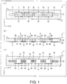
Fig. 1 is a diagram illustrating a configuration of a light emitting device according toEmbodiment 1 of the present invention. -
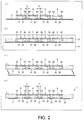
Fig. 2 is a diagram for describing a method of manufacturing the light emitting device according toEmbodiment 1 of the present invention. -
Fig. 3 is a diagram showing deviation amounts from designed numerical values of mounting distances of light emitting diode (LED) elements in the light emitting device according to the present embodiment. -
Fig. 4 is a diagram illustrating a structure of a light emitting device according toEmbodiment 2 of the present invention. -
Fig. 5 is a diagram illustrating a structure of a light emitting device according toEmbodiment 6 of the present invention. -
FIG. 6 is a diagram illustrating a configuration of a light emitting device according to a conventional technology. -
Embodiment 1 according to the present invention will be described below with reference toFigs. 1 to 3 . -
Fig. 1 is a diagram illustrating a configuration of alight emitting device 1 according toEmbodiment 1 of the present invention.Fig. 1(a) is a diagram of thelight emitting device 1 viewed from a light emitting surface (front surface) thereof,Fig. 1(b) is a diagram of thelight emitting device 1 viewed from a surface perpendicular to the light emitting surface (side surface), andFig. 1(c) is a diagram of thelight emitting device 1 viewed from a surface opposite to the light emitting surface (back surface). - As illustrated in
Fig. 1 , thelight emitting device 1 includes a resin moldedbody 2, LED elements (light emitting diode elements, light emitting elements) 3 to 6, andinterconnections 71 to 75. - The resin molded
body 2 serves as a base of thelight emitting device 1 and is formed of any of various types of resin materials. As such a material, polycarbonate (PC) or acrylonitrile butadiene styrene (ABS) can be exemplified. - The
LED elements 3 to 6 are surface mounted device (SMD) type LED elements. As illustrated inFig. 1 , theLED element 3 includes abase portion 31, alight emitting unit 32, an anode 33 (electrode), and a cathode 34 (electrode). TheLED element 4 includes abase portion 41, alight emitting unit 42, an anode 43 (electrode), and a cathode 44 (electrode). TheLED element 5 includes abase portion 51, alight emitting unit 52, an anode 53 (electrode), and a cathode 54 (electrode). TheLED element 6 includes abase portion 61, alight emitting unit 62, an anode 63 (electrode), and a cathode 64 (electrode). - The
base portion 31 is a main body portion of theLED element 3. Thelight emitting unit 32 made of an LED is formed on a surface of thebase portion 31. When theLED element 3 emits light, the light is emitted from thelight emitting unit 32. Theanode 33 and thecathode 34 are connection electrodes connected to an external part of thelight emitting device 1 or to any one of theother LED elements 4 to 6 in thelight emitting device 1. Theanode 33 and thecathode 34 are formed on the back surface opposite to the front surface of thebase portion 31. - Since detailed configuration of the
LED elements 4 to 6 is the same as that of theLED element 3, detailed description thereof will be omitted. - The
LED elements 3 to 6 are embedded in the resin moldedbody 2. As illustrated inFig. 1 , fourLED elements 3 to 6 are linearly disposed in thelight emitting device 1. As illustrated inFig. 1(a) , thelight emitting units 32 to 62 are exposed on afront surface 21 of the resin moldedbody 2. Therefore, as indicated by arrows inFig. 1(b) , when thelight emitting device 1 emits light, the light is emitted from thefront surface 21 of the resin moldedbody 2. - As illustrated in
Fig. 1(c) , theanodes 33 to 63 and thecathodes 34 to 64 are exposed on aback surface 23 opposite to thefront surface 21 of the resin moldedbody 2. - The
interconnections 71 to 75 are formed on theback surface 23 of the resin moldedbody 2 and are connected to at least one of the correspondinganodes 33 to 63 orcathodes 34 to 64. Theinterconnections 71 to 75 are formed by printing on theback surface 23 of the resin moldedbody 2 by a printing method using silver ink or the like, for example. Therefore, a solder material is unnecessary for connecting theinterconnections 71 to 75 with theanodes 33 to 63 or thecathodes 34 to 64. - As illustrated in
Fig. 1 , one end of theinterconnection 71 is connected to theanode 33. The other end of theinterconnection 71 is connected to a drive circuit (not illustrated) outside thelight emitting device 1. One end of theinterconnection 72 is connected to thecathode 34 and the other end is connected to theanode 43. In this manner, theinterconnection 72 serves the role of connecting theLED element 3 and theLED element 4. - One end of the
interconnection 73 is connected to thecathode 44 and the other end is connected to theanode 53. In this manner, theinterconnection 73 serves the role of connecting theLED element 4 and theLED element 5. - One end of the
interconnection 74 is connected to thecathode 54 and the other end is connected to theanode 63. In this manner, theinterconnection 74 serves the role of connecting theLED element 5 and theLED element 6. - One end of the
interconnection 75 is connected to thecathode 64. The other end of theinterconnection 75 is connected to a drive circuit (not illustrated) outside thelight emitting device 1. - As described above, the
LED elements 3 to 6 are connected in series with each other using theinterconnections 71 to 75. Therefore, when theLED elements 3 to 6 are driven all at once by the external drive circuit, theLED elements 3 to 6 emit light at the same time. - The
light emitting device 1 according to the present embodiment is suitably used for an optical printer head or the like mounted on an electrophotographic printer. Particularly, since the light emitting surface of thelight emitting device 1 and a surface on which theinterconnections 71 to 75 are formed respectively correspond to the front surface and the back surface of thelight emitting device 1, it is possible to improve assemblability of the drive circuit for driving theLED elements 3 to 6 or the other parts constituting the printer with thelight emitting device 1. -
Fig. 2 is a diagram for describing a method of manufacturing thelight emitting device 1 according to the present embodiment. A method of manufacturing thelight emitting device 1 according to the present embodiment will be described below with reference toFig. 2 . - First, as illustrated in
Fig. 2(a) , atemporary fixing film 11 for temporarily fixing theLED elements 3 to 6 is prepared and theLED elements 3 to 6 are temporarily fixed to thetemporary fixing film 11. As thetemporary fixing film 11, for example, a film made of polyethylene terephthalate (PET) can be used. - In the present embodiment, the
LED elements 3 to 6 are temporarily fixed to thetemporary fixing film 11 using an adhesive or the like so that theanodes 33 to 63 and thecathodes 34 to 64 of theLED elements 3 to 6 come into contact with thetemporary fixing film 11. For this temporary fixing, for example, an ultraviolet curable adhesive (not illustrated) applied to thetemporary fixing film 11 can be used. Specifically, GL-3005H made by Gluelabo Ltd. is used as the adhesive, and the adhesive is applied to thetemporary fixing film 11 made of PET having a thickness of 50 µm to have a thickness of 2 to 3 µm. - Then, positions of the
LED elements 3 to 6 in thetemporary fixing film 11 are determined, and theLED elements 3 to 6 are installed at the determined positions on thetemporary fixing film 11. Thereafter, thetemporary fixing film 11 and theLED elements 3 to 6 are irradiated with ultraviolet rays of 3000 mJ/cm2 to cure the adhesive. As a result, theLED elements 3 to 6 are temporarily fixed to thetemporary fixing film 11. - Next, as illustrated in
Fig. 2(b) , thetemporary fixing film 11 on which theLED elements 3 to 6 are temporarily fixed in the temporary fixing step is disposed in a gap between amold 12 and amold 13, and a resin material is injected into the gap. Thereby, injection molding of the resin material is performed so that theLED elements 3 to 6 are embedded in the resin moldedbody 2. - As the resin material used for this step, various types of resin materials such as polycarbonate (PC) and acrylonitrile butadiene styrene (ABS) can be exemplified. When PC is used, the PC is used at an injection temperature of 270 °C and an injection pressure of 100 Mpa. When ABS is used, the ABS is used at an injection temperature of 180 °C and an injection pressure of 20 kgf/cm2.
- Next, as illustrated in
Fig. 2(c) , the injection molded product obtained in the injection molding step is taken out from the gap between themold 12 and themold 13, and then thetemporary fixing film 11 is peeled off from the injection molded product. Thereby, thelight emitting units 32 to 62 of theLED elements 3 to 6 are exposed on the front surface of the resin moldedbody 2. On the other hand, theanodes 33 to 63 and thecathodes 34 to 64 of theLED elements 3 to 6 are exposed on the back surface of the resin moldedbody 2. - Further, the PET film used as the
temporary fixing film 11 is greatly deformed by heat at the time of injection molding in the injection molding step and is in a state in which it has been peeled off from the injection molded product. Therefore, thetemporary fixing film 11 can be easily separated from the injection molded product. - Finally, as illustrated in
Fig. 2(d) , theinterconnections 71 to 75 connected to theanodes 33 to 63 and thecathodes 34 to 64 of each of theLED elements 3 to 6 exposed on theback surface 23 of the resin moldedbody 2 are formed on theback surface 23 of the resin moldedbody 2. Thereby, thelight emitting device 1 is completed. - Various methods can be used for forming the
interconnections 71 to 75. A method of print-forming theinterconnections 71 to 75 by jetting a conductive material (for example, silver ink or the like) using an ink jet printer or the like, a method of forming theinterconnections 71 to 75 using an aerosol, a method of forming theinterconnections 71 to 75 using a dispenser, or the like can be exemplified. -
Fig. 3 is a diagram showing deviation amounts from designed numerical values of mounting distances of theLED elements 3 to 6 in thelight emitting device 1 according to the present embodiment. As illustrated inFig. 3 , deviation amounts from designed numerical values of a mounting distance a between theLED element 3 and theLED element 4 and a mounting distance b between theLED element 4 and theLED element 5 in the temporary fixing step (at the time of temporary fixing of theLED elements 3 to 6) illustrated inFig. 2(a) were -12 µm and +21 µm. On the other hand, deviation amounts from designed numerical values of the mounting distance a between theLED element 3 and theLED element 4 and the mounting distance b between theLED element 4 and theLED element 5 in the interconnection formation step (at the time of completion of the light emitting device 1) illustrated inFig. 2(b) were +14 µm and +39 µm. - As shown in
Fig. 3 , the deviation amounts of the mounting distances of theLED elements 3 to 6 at the time of temporary fixing hardly change even at the time of completion of thelight emitting device 1. Therefore, according to the present embodiment, it is possible to manufacture thelight emitting device 1 in which theLED elements 3 to 6 are disposed on thetemporary fixing film 11 at the positions at the time of temporary fixing. - The
light emitting device 1 illustrated inFig. 1 does not have a printed circuit board which is necessary for a light emitting device according to a conventional technology and also does not need a solder material for connecting interconnections and electrodes (an anode and a cathode). Thereby, the following effects which contribute to miniaturization and thinning of thelight emitting device 1 can be obtained. - (1) Since a height of the
light emitting device 1 can be made small enough that it is approximately equal to a height of theLED elements 3 to 6, thinning of thelight emitting device 1 can be achieved. - (2) Since spaces between the
LED elements 3 to 6 which are necessary for connecting the electrodes of the LED elements and the interconnections by a solder material in the conventional technology are not necessary for thelight emitting device 1, pitches (intervals between theLED elements 3 to 6) when theLED elements 3 to 6 are mounted on thelight emitting device 1 can be made smaller than those in the conventional technology.
In addition, in the method of manufacturing thelight emitting device 1 according to the present embodiment, since theLED elements 3 to 6 are embedded in the resin moldedbody 2 to be fixed in the resin moldedbody 2, mounting positions of theLED elements 3 to 6 of thelight emitting device 1 are accurately determined according to installation positions of theLED elements 3 to 6 on thetemporary fixing film 11 in the temporary fixing step. Thereby, the following effects can be obtained. - (3) As accuracy of the mounting positions in a planar direction (X-Y direction) of the
LED elements 3 to 6 in thelight emitting device 1, high accuracy of about ±50 µm in the LED element mounting machine can be obtained. - (4) Further, positional accuracy in a height direction (H direction) of the
LED elements 3 to 6 in thelight emitting device 1 can be reduced to within several µm of a variation degree of a coating thickness of the adhesive used in the temporary fixing step.
In addition, since a heat treatment at 260 °C or higher required for curing a solder material in the conventional technology is unnecessary in the method of manufacturing thelight emitting device 1 according to the present embodiment, the following effects can be obtained. - (5) Since high temperature heat is not applied to the
LED elements 3 to 6, it is possible to prevent a change in light emitting characteristics of theLED elements 3 to 6.
Further, since the method of manufacturing thelight emitting device 1 according to the present embodiment does not include an additional step of the printed circuit board and a complicated step such as assembling the other members with theLED elements 3 to 6, the following effects can be obtained. - (6) It is possible to eliminate a factor lowering a manufacturing yield of the
light emitting device 1, and to lower part costs and manufacturing costs of thelight emitting device 1. - The arrangement of the
LED elements 3 to 6 illustrated inFig. 1 is merely an example. A plurality of LED elements included in thelight emitting device 1 may be disposed in a matrix form inside the resin moldedbody 2, for example. Further, thelight emitting device 1 may be configured to include a light emitting element other than theLED elements 3 to 6 such as an organic electro luminescence (EL) element or the like. -
Embodiment 2 of the present invention will be described below with reference toFig 4 . For convenience of description, members having the same functions as those described in the above embodiment will be denoted by the same reference signs, and description thereof will be omitted. - In
Embodiment 1, thelight emitting device 1 having the structure in which thelight emitting units 32 to 62 of theLED elements 3 to 6 are exposed on the front surface of the resin moldedbody 2 has been described. However, the present invention is not limited thereto, and thelight emitting device 1 may have a structure in which thelight emitting units 32 to 62 are embedded in the resin moldedbody 2. In this case, it is necessary for the resin moldedbody 2 to have a certain level of light transmittance. -
Fig. 4 is a diagram illustrating a structure of alight emitting device 1 according toEmbodiment 2 of the present invention. As illustrated inFig. 4 , on an upper portion of light emittingunits 32 to 62 of thelight emitting device 1 according to the present embodiment, there may be a predetermined optical part (structure) for imparting directivity to light emitted from thelight emitting units 32 to 62. In an example ofFig. 4 , alens 24 is provided on an upper portion of thelight emitting unit 32, aprismatic polyhedron 25 is provided on an upper portion of thelight emitting unit 42, and a concave-shapedlight reflecting portion 26 is provided on an upper portion of thelight emitting unit 52. Thelens 24, thepolyhedron 25, and thelight reflecting portion 26 are formed as portions of a resin moldedbody 2 at the time of molding the resin moldedbody 2. - In the conventional technology, it is necessary to separately prepare such a member imparting directivity as a part separate from the LED element and to assemble the member to the LED element. This leads to problems such as complicated assembly of the light emitting device and high manufacturing costs. Further, in a
light emitting device 101 having a configuration in which a plurality ofLED elements 103 are mounted in an array as illustrated inFig. 6 , since there is a possibility of mounting positions of each of theLED elements 103 deviating, there is a problem in that high precision adjustment is required when optical parts such as the lens prepared as separate parts are aligned with theLED elements 103. Alternatively, as a result of poor positional alignment, there is also a problem in that a defect rate of thelight emitting device 101 increases. - On the other hand, in the
light emitting device 1 according to the present embodiment, theLED elements 3 to 6 are embedded in the resin moldedbody 2, and at the same time, optical parts such as thelens 24 are injection molded at embedded positions of theLED elements 3 to 6. Thereby, it is unnecessary to assemble optical parts such as the lens prepared as separate parts from theLED elements 3 to 6 to theLED elements 3 to 6. In addition, since there is little variation in mounting positions of theLED elements 3 to 6 as shown inFig. 3 , highly accurate positional adjustment between theLED elements 3 to 6 and thelens 24 or the like is unnecessary. Thereby, an incidence of defective products of thelight emitting device 1 can be reduced. -
Embodiment 3 according to the present invention will be described below. For convenience of description, members having the same functions as those described in the above embodiment will be denoted by the same reference signs, and description thereof will be omitted. - In the conventional technology illustrated in
Fig. 6 , light emission from alight emitting surface 122 of eachLED element 103 leaks, for example, also towardadjacent LED elements 103 in addition to an upper direction indicated by arrows inFig. 6 . Thereby, light emission from eachLED element 103 interferes with each other. When thelight emitting device 101 in such a state is used for an optical printer head or the like, such a problem in which a dot image is blurred or written and stored image qualities are deteriorated occurs. - Therefore, as a countermeasure against such a problem, in the present embodiment, a resin material having a light reflectance of 90% or higher is used as a material of the resin molded
body 2 constituting thelight emitting device 1. As an example of such a material, FULL BRIGHT (manufactured by Panasonic Co., Ltd.) which is a polypropylene (PP) based resin, EHR GRADE (manufactured by Mitsubishi Engineering-Plastic Corporation) which is a polycarbonate (PC) based resin, or the like can be exemplified. - In the
light emitting device 1 having the resin moldedbody 2 formed of such a material, it is possible to prevent light emitted from thelight emitting units 32 to 62 of therespective LED elements 3 to 6 from leaking toward theadjacent LED elements 3 to 6. Therefore, an effect of reducing interference between respective light emissions is obtained. -
Embodiment 4 according to the present invention will be described below. For convenience of explanation, members having the same functions as those described in the above embodiment are denoted by the same reference numerals, and description thereof is omitted. - In
Embodiment 3, an example in which a resin material having a high light reflectance is used as the material of the resin moldedbody 2 in which theLED elements 3 to 6 are embedded has been described. However, the present invention is not limited thereto, and it is also possible to use a transparent resin material having a high light transmittance as the material of the resin moldedbody 2. - In the
light emitting device 1 according to the present embodiment, as the material of the resin moldedbody 2 included in thelight emitting device 1, a material having a light transmittance which transmits 80% or higher of visible light is used. As such a material, for example, transparent polycarbonate (PC), transparent acrylic resin, or the like can be exemplified. - In the
light emitting device 1 having the resin moldedbody 2 formed of such a material, a light emitting area of thelight emitting device 1 is wide, and light emission with good visibility and decorative properties is emitted from thelight emitting device 1. Therefore, thelight emitting device 1 can be suitably used in a switch having a light emitting display portion, an illumination device, or the like. -
Embodiment 5 according to the present invention will be described below. For convenience of explanation, members having the same functions as those described in the above embodiment are denoted by the same reference numerals, and description thereof is omitted. - In
Embodiment 1, a method of using PC (polycarbonate) and ABS (acrylonitrile butadiene styrene) as the material of the resin moldedbody 2 in which theLED elements 3 to 6 are embedded has been described, but the present invention is not limited thereto. As the material of the resin moldedbody 2, a material having high thermal conductivity can also be used. - In recent years, an application of LED elements as light parts such as lighting has increased and problems occur due to heat generation of the LED elements caused by high luminance of LED elements accompanied by such a demand. Conventionally, as a countermeasure against such heat generation of LED elements, in the
light emitting device 101 according to the conventional technology illustrated inFig. 6 , a method of using a metal such as an aluminum material for a printedcircuit board 102, a method of using a special voltage boosting circuit to minimize heat generation of the LED elements, a method of using an electric wire used as interconnections of LED elements as a heat dissipation body, or the like is employed. - However, with such a conventional method, a problem occurs in that manufacturing costs of the
light emitting device 101 increase due to an increase in substrate processing cost or complication of circuits, or a problem occurs in that sufficient heat dissipation cannot be obtained due to limitation of a size of thelight emitting device 101. - Therefore, as a countermeasure against such a problem, in the
light emitting device 1 according to the present embodiment, a material having thermal conductivity of 1 W1m·K or higher is used as the material of the resin moldedbody 2. As such a material, for example, a nylon-based resin mixed with TORELINA H718LB (manufactured by Toray Industries, Inc.) or high thermal conductive insulating filler manufactured by Unitika Ltd. can be exemplified. - In the
light emitting device 1 having the resin moldedbody 2 formed of such a material, since the resin moldedbody 2 acts as a heat sink of a large area for dissipating the heat generated by theLED elements 3 to 6, it is possible to prevent problems caused by heat generation of theLED elements 3 to 6. -
Embodiment 6 of the present invention will be described below with reference toFig 5 . For convenience of description, members having the same functions as those described in the above embodiment will be denoted by the same reference signs, and description thereof will be omitted. - In
Embodiment 1, thelight emitting device 1 in which only theLED elements 3 to 6 are embedded in the resin moldedbody 2 has been exemplified. It is necessary to connect a drive circuit to thislight emitting device 1 as a separate part for driving theLED elements 3 to 6. However, the present invention is not limited thereto, and various types of electronic parts (chip parts) such as a drive integrated circuit (IC), a resistor, a capacitor, and the like which constitute the drive circuit for operating theLED elements 3 to 6 can be embedded in the resin moldedbody 2 in which theLED elements 3 to 6 are embedded. Thus, it is possible to manufacture a light emitting electronic device capable of operating the LED elements merely by supplying power. -
Fig. 5 is a diagram illustrating a configuration of alight emitting device 1a according toEmbodiment 6 of the present invention.Fig. 5(a) is a diagram of thelight emitting device 1a viewed from a light emitting surface (front surface) thereof,Fig. 5(b) is a diagram of thelight emitting device 1a viewed from a surface perpendicular to the light emitting surface (side surface),Fig. 5(c) is a diagram of thelight emitting device 1 viewed from a surface opposite to the light emitting surface (back surface). - As illustrated in
Fig. 5 , thelight emitting device 1a includes a resin moldedbody 2, anLED element 3, anLED element 4, anelectronic part 81, anelectronic part 82, and anelectronic part 83 as well as aninterconnection 71, aninterconnection 72, andinterconnections 91 to 95. - The
electronic parts 81 to 83 are various types of electronic parts such as a drive IC, a resistor, and a capacitor, which constitute a drive circuit. Theelectronic parts 81 to 83 include connection electrodes (anode and cathode) (not illustrated) formed on their back surfaces, and these connection electrodes are embedded in the resin moldedbody 2 in a form of being exposed on theback surface 23 of the resin moldedbody 2. - The
interconnections 91 to 95 are interconnections connected to the connection electrodes of theelectronic parts 81 to 83 and are formed on theback surface 23 of the resin moldedbody 2 by a printing method using silver ink or the like as in theinterconnections electronic parts 81 to 83 and theinterconnections 91 to 95 is unnecessary. - As illustrated in
Fig. 5(c) , in thelight emitting device 1a, one end of theinterconnection 91 is connected to theelectronic part 82 and the other end is connected to the other end of theinterconnection 71. One end of theinterconnection 92 is connected to theelectronic part 81 and the other end is connected to acathode 44. One end of theinterconnection 93 is connected to theelectronic part 83 and the other end is connected to theelectronic part 81. One end of theinterconnection 94 is connected to a power supply (not illustrated) outside thelight emitting device 1a, and the other end is connected to theelectronic part 82. One end of theinterconnection 95 is connected to the power supply (not illustrated) outside thelight emitting device 1a, and the other end is connected to theelectronic part 83. - When the above configuration is employed, power from the power supply is supplied to the drive circuit constituted by the
electronic parts 81 to 83. Also, since theLED elements LED elements body 2 in which theLED elements light emitting device 1a. Thus, it is possible to reduce processing costs or interconnection costs for connecting a drive circuit to thelight emitting device 1a. - In order to embed the
electronic parts 81 to 83 according to the present embodiment in the resin moldedbody 2, a step similar to the step of fixing theLED elements 3 to 6 to thetemporary fixing film 11 inEmbodiment 1 described with reference toFig. 2(a) can be used. Further, in order to form theinterconnections 91 to 95 on theback surface 23 of the resin moldedbody 2, a step similar to the step of print-forming theinterconnections 71 to 75 inEmbodiment 1 described with reference toFig. 2(d) can be used. - The present invention is not limited to each of the above-described embodiments, and various modifications are possible within the scope indicated in the claims. Embodiments obtained by appropriately combining technical methods disclosed in different embodiments are also included in the technical scope of the present invention. New technical features can also be formed by combining technical methods disclosed in each embodiment.
- In order to solve the above problems, a light emitting device according to one aspect of the present invention includes a resin molded body, a light emitting element having at least a light emitting unit and an electrode and embedded in the resin molded body so that the light emitting unit faces a front surface of the resin molded body and the electrode is exposed on a back surface opposite to the front surface of the resin molded body, and an interconnection formed on the back surface of the resin molded body and connected to the electrode.
- According to the above configuration, the light emitting element is mounted on the light emitting device in a form of being embedded in the resin molded body. Therefore, since a printed circuit board for mounting the light emitting element is not required, a height of the light emitting device can be made substantially the same as a height of the light emitting element (resin molded body). In addition, since the interconnection connected to the electrode of the light emitting element exposed on the back surface of the resin molded body can be formed by printing, there is no need to use a solder material for connection. Thereby, since spaces for the solder material between the light emitting elements are unnecessary, mounting pitches between the light emitting elements can be minimized.
- As described above, according to the present invention, it is possible to realize a more compact and thinner light emitting device.
- The light emitting device according to one aspect of the present invention is further characterized in that the light emitting unit is exposed on the front surface.
- According to the above configuration, light from the light emitting unit is emitted from the front surface of the light emitting device without being obstructed by the resin molded body. Further, the resin molded body can be formed of a material having a low light transmittance.
- The light emitting device according to one aspect of the present invention is further characterized in that the resin molded body is formed of a resin material having a light reflectance of 90% or higher.
- According to the above configuration, in a case in which the light emitting device includes a plurality of light emitting elements, since it is possible to prevent light emitted from each of the light emitting elements from leaking toward adjacent light emitting elements, interference between the respective light emissions can be reduced.
- The light emitting device according to one aspect of the present invention is further characterized in that the resin molded body is formed of a resin material having a light reflectance of 80% or higher.
- According to the above configuration, the light emitting device emits light with good visibility and decorative properties.
- The light emitting device according to one aspect of the present invention is further characterized in that the resin molded body is formed of a resin material having thermal conductivity of 1 W/m·K or higher.
- According to the above configuration, since the heat generated by the light emitting element is easily released to the outside of the light emitting device through the resin molded body, the problem caused by heat generation can be prevented.
- The light emitting device according to one aspect of the present invention is further characterized in that a plurality of light emitting elements are embedded in the resin molded body and the electrodes included in the respective light emitting elements are connected to each other by the interconnections.
- According to the above configuration, it is possible to realize a light emitting device including a plurality of light emitting elements.
- The light emitting device according to one aspect of the present invention is further characterized in that it further includes a drive circuit embedded in the resin molded body and driving the light emitting elements, in which the electrode and the drive circuit are connected to each other by the interconnection.
- According to the above configuration, a light emitting device which emits light merely by supplying power can be realized.
- The light emitting device according to one aspect of the present invention is further characterized in that an optical part which imparts directivity to light from the light emitting unit is formed on an upper portion of the light emitting unit of the resin molded body.
- According to the above configuration, light to which directivity is imparted can be emitted from the light emitting device.
- The light emitting device according to one aspect of the present invention is further characterized in that the light emitting element is a light emitting diode element.
- According to the above configuration, a light emitting device with low power consumption can be realized.
- In order to solve the above problems, a method of manufacturing a light emitting device according to one aspect of the present invention includes a step of temporarily fixing a light emitting element having at least a light emitting unit and an electrode on a temporary fixing film in a form in which the electrode comes into contact with the temporary fixing film, a step of forming a resin molded body in which the light emitting element is embedded by disposing the temporary fixing film to which the light emitting element is temporarily fixed in a gap in a mold and injecting a resin material into the gap, a step of peeling off the temporary fixing film from the resin molded body, and a step of forming an interconnection connected to the electrode on a back surface of the resin molded body from which the electrode is exposed.
- According to the above configuration, it is possible to more easily manufacture a more compact and thinner light emitting device.
-
- 1, 1a Light emitting device
- 2 Resin molded body
- 3 to 6 LED element (light emitting element)
- 11 Temporary fixing film
- 12, 13 Mold
- 24 Lens
- 25 Polyhedron
- 26 Light reflecting portion
- 31 to 61 Base portion
- 32 ∼ 62 Light emitting unit
- 33 to 63 Anode (electrode)
- 34 to 64 Cathode (electrode)
- 71 to 75, 91 to 95 Interconnection
- 81 to 83 Electronic part
Claims (10)
- A light emitting device comprising:a resin molded body;a light emitting element having at least a light emitting unit and an electrode and that is embedded in the resin molded body so that the light emitting unit faces a front surface of the resin molded body and the electrode is exposed on a back surface opposite to the front surface of the resin molded body; andan interconnection formed on the back surface of the resin molded body and connected to the electrode.
- The light emitting device according to claim 1, wherein the light emitting unit is exposed on the front surface.
- The light emitting device according to claim 2, wherein the resin molded body is formed of a resin material having a light reflectance of 90% or higher.
- The light emitting device according to claim 1 or 2, wherein the resin molded body is formed of a resin material having a light reflectance of 80% or higher.
- The light emitting device according to any one of claims 1 to 4, wherein the resin molded body is formed of a resin material having thermal conductivity of 1 W/m·K or higher.
- The light emitting device according to any one of claims 1 to 5, wherein a plurality of light emitting elements are embedded in the resin molded body and the electrodes included in the respective light emitting elements are connected to each other by the interconnection.
- The light emitting device according to any one of claims 1 to 5, further comprising a drive circuit embedded in the resin molded body and driving the light emitting element, wherein the electrode and the drive circuit are connected to each other by the interconnection.
- The light emitting device according to any one of claims 1 to 7, wherein an optical part which imparts directivity to light from the light emitting unit is formed on an upper portion of the light emitting unit of the resin molded body.
- The light emitting device according to any one of claims 1 to 8, wherein the light emitting element is a light emitting diode element.
- A method of manufacturing a light emitting device comprising:a step of temporarily fixing a light emitting element having at least a light emitting unit and an electrode on a temporary fixing film in a form in which the electrode comes into contact with the temporary fixing film;a step of forming a resin molded body in which the light emitting element is embedded by disposing the temporary fixing film to which the light emitting element is temporarily fixed in a gap in a mold and injecting a resin material into the gap;a step of peeling off the temporary fixing film from the resin molded body; anda step of forming an interconnection connected to the electrode on a back surface of the resin molded body from which the electrode is exposed.
Applications Claiming Priority (2)
| Application Number | Priority Date | Filing Date | Title |
|---|---|---|---|
| JP2016013707A JP2017135253A (en) | 2016-01-27 | 2016-01-27 | Light-emitting device and method of manufacturing the same |
| PCT/JP2016/084781 WO2017130544A1 (en) | 2016-01-27 | 2016-11-24 | Light emitting device, and manufacturing method of light emitting device |
Publications (3)
| Publication Number | Publication Date |
|---|---|
| EP3410499A1 true EP3410499A1 (en) | 2018-12-05 |
| EP3410499A4 EP3410499A4 (en) | 2019-08-14 |
| EP3410499B1 EP3410499B1 (en) | 2023-05-10 |
Family
ID=59398137
Family Applications (1)
| Application Number | Title | Priority Date | Filing Date |
|---|---|---|---|
| EP16888128.2A Active EP3410499B1 (en) | 2016-01-27 | 2016-11-24 | Light emitting device, and manufacturing method of light emitting device |
Country Status (6)
| Country | Link |
|---|---|
| US (1) | US20180233640A1 (en) |
| EP (1) | EP3410499B1 (en) |
| JP (1) | JP2017135253A (en) |
| CN (1) | CN107851697A (en) |
| TW (1) | TWI643366B (en) |
| WO (1) | WO2017130544A1 (en) |
Families Citing this family (4)
| Publication number | Priority date | Publication date | Assignee | Title |
|---|---|---|---|---|
| JP7003478B2 (en) * | 2017-08-02 | 2022-01-20 | オムロン株式会社 | Electronic device and its manufacturing method |
| US10522709B1 (en) * | 2017-12-05 | 2019-12-31 | Facebook Technologies, Llc | Method of direct wafer mapping by determining operational LEDs from non-operational LEDs using photo-reactive elastomer deposition |
| KR102626051B1 (en) * | 2018-08-14 | 2024-01-19 | 삼성디스플레이 주식회사 | Light emitting diode, pixel structure including the light emitting diode, and method of manufacturing the same |
| KR102818698B1 (en) | 2020-01-22 | 2025-06-10 | 엘지전자 주식회사 | Display device using semiconductor light emitting device |
Family Cites Families (21)
| Publication number | Priority date | Publication date | Assignee | Title |
|---|---|---|---|---|
| JPS6425582A (en) | 1987-07-22 | 1989-01-27 | Oki Electric Ind Co Ltd | Mounting construction of led device |
| JP2962008B2 (en) | 1991-11-29 | 1999-10-12 | 松下電器産業株式会社 | Sequential control device |
| JP3690852B2 (en) | 1995-12-27 | 2005-08-31 | シャープ株式会社 | Surface-emitting display device |
| JPH11219961A (en) | 1998-02-03 | 1999-08-10 | Oki Electric Ind Co Ltd | Optical semiconductor module mounting structure and mounting method |
| JP4279207B2 (en) * | 2004-06-18 | 2009-06-17 | アルプス電気株式会社 | Input device and display input device using this input device |
| JP4960099B2 (en) * | 2004-10-04 | 2012-06-27 | 株式会社東芝 | Light emitting device and lighting apparatus or liquid crystal display device using the same |
| JP4910518B2 (en) | 2006-07-05 | 2012-04-04 | 富士ゼロックス株式会社 | Method for manufacturing organic electroluminescent device |
| JP5515223B2 (en) * | 2008-02-12 | 2014-06-11 | ソニー株式会社 | Semiconductor device |
| DE102009036621B4 (en) * | 2009-08-07 | 2023-12-21 | OSRAM Opto Semiconductors Gesellschaft mit beschränkter Haftung | Optoelectronic semiconductor component |
| JP5775002B2 (en) * | 2010-01-29 | 2015-09-09 | シチズン電子株式会社 | Method for manufacturing light emitting device |
| JP2011253925A (en) * | 2010-06-02 | 2011-12-15 | Toshiba Corp | Method of manufacturing light-emitting device |
| JP5648422B2 (en) * | 2010-10-29 | 2015-01-07 | 日亜化学工業株式会社 | Light emitting device and manufacturing method thereof |
| JP2013021175A (en) * | 2011-07-12 | 2013-01-31 | Toshiba Corp | Semiconductor light-emitting element |
| DE102011080458A1 (en) * | 2011-08-04 | 2013-02-07 | Osram Opto Semiconductors Gmbh | OPTOELECTRONIC ARRANGEMENT AND METHOD FOR PRODUCING AN OPTOELECTRONIC ARRANGEMENT |
| EP2913856A4 (en) * | 2012-10-25 | 2016-01-06 | Panasonic Ip Man Co Ltd | LIGHT EMITTING DEVICE, ITS MANUFACTURING METHOD, AND BODY HAVING A LIGHT EMITTING DEVICE MOUNTED THEREON |
| JP5943898B2 (en) * | 2012-11-29 | 2016-07-05 | 日東電工株式会社 | Method for manufacturing thermosetting resin sheet and electronic component package |
| KR102091994B1 (en) * | 2012-12-21 | 2020-03-23 | 다우 실리콘즈 코포레이션 | Layered polymer structures and methods |
| DE102013207611A1 (en) * | 2013-04-25 | 2014-10-30 | Osram Gmbh | Lighting device with optoelectronic component |
| JP6259329B2 (en) * | 2014-03-14 | 2018-01-10 | シチズン電子株式会社 | LED light emitting device |
| EP3547379A1 (en) * | 2014-03-14 | 2019-10-02 | Citizen Electronics Co., Ltd. | Light emitting apparatus |
| JP6354285B2 (en) * | 2014-04-22 | 2018-07-11 | オムロン株式会社 | Resin structure in which electronic component is embedded and method for manufacturing the same |
-
2016
- 2016-01-27 JP JP2016013707A patent/JP2017135253A/en active Pending
- 2016-11-24 WO PCT/JP2016/084781 patent/WO2017130544A1/en not_active Ceased
- 2016-11-24 US US15/750,836 patent/US20180233640A1/en not_active Abandoned
- 2016-11-24 CN CN201680046141.4A patent/CN107851697A/en active Pending
- 2016-11-24 EP EP16888128.2A patent/EP3410499B1/en active Active
- 2016-12-15 TW TW105141492A patent/TWI643366B/en active
Also Published As
| Publication number | Publication date |
|---|---|
| TW201727950A (en) | 2017-08-01 |
| WO2017130544A1 (en) | 2017-08-03 |
| EP3410499B1 (en) | 2023-05-10 |
| TWI643366B (en) | 2018-12-01 |
| CN107851697A (en) | 2018-03-27 |
| JP2017135253A (en) | 2017-08-03 |
| EP3410499A4 (en) | 2019-08-14 |
| US20180233640A1 (en) | 2018-08-16 |
Similar Documents
| Publication | Publication Date | Title |
|---|---|---|
| EP3410500B1 (en) | Light emitting device, backlight device, and manufacturing method of light emitting device | |
| EP3410499B1 (en) | Light emitting device, and manufacturing method of light emitting device | |
| JP5097461B2 (en) | Liquid crystal display and backlight module thereof | |
| US20090322214A1 (en) | Organic light emitting diode display and method of manufacturing the same | |
| US7766499B2 (en) | Light source unit, backlight unit and liquid crystal display including the same, and method thereof | |
| US8764209B2 (en) | Light module | |
| US20160252231A1 (en) | Light emitting device | |
| CN109087584B (en) | Display device | |
| US20210183897A1 (en) | Substrate and method for manufacturing the same, display panel, and display apparatus | |
| US8897035B2 (en) | Container and display device including the same | |
| JP5110325B2 (en) | Light emitting device and manufacturing method thereof | |
| US20240204149A1 (en) | Display device comprising display module, and method for manufacturing same | |
| US8330053B2 (en) | Optoelectronic device and method for producing an optoelectronic device | |
| CN103366647A (en) | LED display unit module | |
| KR101164958B1 (en) | Heat radiating printed circuit board unified bracket for backlight unit and metal mask used therefor | |
| KR100963092B1 (en) | LED lighting and manufacturing method integrating exterior, heat sink and printed circuit | |
| CN117941071B (en) | Display device | |
| US20240203910A1 (en) | Display device including display module and method for manufacturing same | |
| KR20110051718A (en) | Bracket-integrated heat dissipation PCB for backlight unit, chassis structure with same and manufacturing method thereof | |
| KR20150072814A (en) | Light emitting diode module with intergrated heat sink | |
| JP5803749B2 (en) | Planar light emitter and lighting device | |
| KR102425807B1 (en) | Display device | |
| TW202325116A (en) | Electronic device | |
| CN118022196A (en) | A flexible light-emitting module and light therapy beauty instrument | |
| KR20150033489A (en) | Coupling type illumination module and illumination device having the same |
Legal Events
| Date | Code | Title | Description |
|---|---|---|---|
| STAA | Information on the status of an ep patent application or granted ep patent |
Free format text: STATUS: THE INTERNATIONAL PUBLICATION HAS BEEN MADE |
|
| PUAI | Public reference made under article 153(3) epc to a published international application that has entered the european phase |
Free format text: ORIGINAL CODE: 0009012 |
|
| STAA | Information on the status of an ep patent application or granted ep patent |
Free format text: STATUS: REQUEST FOR EXAMINATION WAS MADE |
|
| 17P | Request for examination filed |
Effective date: 20180208 |
|
| AK | Designated contracting states |
Kind code of ref document: A1 Designated state(s): AL AT BE BG CH CY CZ DE DK EE ES FI FR GB GR HR HU IE IS IT LI LT LU LV MC MK MT NL NO PL PT RO RS SE SI SK SM TR |
|
| AX | Request for extension of the european patent |
Extension state: BA ME |
|
| DAV | Request for validation of the european patent (deleted) | ||
| DAX | Request for extension of the european patent (deleted) | ||
| A4 | Supplementary search report drawn up and despatched |
Effective date: 20190715 |
|
| RIC1 | Information provided on ipc code assigned before grant |
Ipc: H01L 33/54 20100101AFI20190709BHEP Ipc: H01L 33/64 20100101ALI20190709BHEP Ipc: H01L 33/62 20100101ALI20190709BHEP Ipc: B29C 45/14 20060101ALI20190709BHEP Ipc: H01L 33/60 20100101ALI20190709BHEP |
|
| STAA | Information on the status of an ep patent application or granted ep patent |
Free format text: STATUS: EXAMINATION IS IN PROGRESS |
|
| 17Q | First examination report despatched |
Effective date: 20200518 |
|
| GRAP | Despatch of communication of intention to grant a patent |
Free format text: ORIGINAL CODE: EPIDOSNIGR1 |
|
| STAA | Information on the status of an ep patent application or granted ep patent |
Free format text: STATUS: GRANT OF PATENT IS INTENDED |
|
| INTG | Intention to grant announced |
Effective date: 20230217 |
|
| RIN1 | Information on inventor provided before grant (corrected) |
Inventor name: KAWAI, WAKAHIRO |
|
| GRAS | Grant fee paid |
Free format text: ORIGINAL CODE: EPIDOSNIGR3 |
|
| GRAA | (expected) grant |
Free format text: ORIGINAL CODE: 0009210 |
|
| STAA | Information on the status of an ep patent application or granted ep patent |
Free format text: STATUS: THE PATENT HAS BEEN GRANTED |
|
| AK | Designated contracting states |
Kind code of ref document: B1 Designated state(s): AL AT BE BG CH CY CZ DE DK EE ES FI FR GB GR HR HU IE IS IT LI LT LU LV MC MK MT NL NO PL PT RO RS SE SI SK SM TR |
|
| REG | Reference to a national code |
Ref country code: GB Ref legal event code: FG4D |
|
| REG | Reference to a national code |
Ref country code: AT Ref legal event code: REF Ref document number: 1567600 Country of ref document: AT Kind code of ref document: T Effective date: 20230515 Ref country code: CH Ref legal event code: EP |
|
| REG | Reference to a national code |
Ref country code: DE Ref legal event code: R096 Ref document number: 602016079428 Country of ref document: DE |
|
| REG | Reference to a national code |
Ref country code: IE Ref legal event code: FG4D |
|
| REG | Reference to a national code |
Ref country code: LT Ref legal event code: MG9D |
|
| REG | Reference to a national code |
Ref country code: NL Ref legal event code: MP Effective date: 20230510 |
|
| REG | Reference to a national code |
Ref country code: AT Ref legal event code: MK05 Ref document number: 1567600 Country of ref document: AT Kind code of ref document: T Effective date: 20230510 |
|
| PG25 | Lapsed in a contracting state [announced via postgrant information from national office to epo] |
Ref country code: SE Free format text: LAPSE BECAUSE OF FAILURE TO SUBMIT A TRANSLATION OF THE DESCRIPTION OR TO PAY THE FEE WITHIN THE PRESCRIBED TIME-LIMIT Effective date: 20230510 Ref country code: PT Free format text: LAPSE BECAUSE OF FAILURE TO SUBMIT A TRANSLATION OF THE DESCRIPTION OR TO PAY THE FEE WITHIN THE PRESCRIBED TIME-LIMIT Effective date: 20230911 Ref country code: NO Free format text: LAPSE BECAUSE OF FAILURE TO SUBMIT A TRANSLATION OF THE DESCRIPTION OR TO PAY THE FEE WITHIN THE PRESCRIBED TIME-LIMIT Effective date: 20230810 Ref country code: NL Free format text: LAPSE BECAUSE OF FAILURE TO SUBMIT A TRANSLATION OF THE DESCRIPTION OR TO PAY THE FEE WITHIN THE PRESCRIBED TIME-LIMIT Effective date: 20230510 Ref country code: ES Free format text: LAPSE BECAUSE OF FAILURE TO SUBMIT A TRANSLATION OF THE DESCRIPTION OR TO PAY THE FEE WITHIN THE PRESCRIBED TIME-LIMIT Effective date: 20230510 Ref country code: AT Free format text: LAPSE BECAUSE OF FAILURE TO SUBMIT A TRANSLATION OF THE DESCRIPTION OR TO PAY THE FEE WITHIN THE PRESCRIBED TIME-LIMIT Effective date: 20230510 |
|
| PG25 | Lapsed in a contracting state [announced via postgrant information from national office to epo] |
Ref country code: RS Free format text: LAPSE BECAUSE OF FAILURE TO SUBMIT A TRANSLATION OF THE DESCRIPTION OR TO PAY THE FEE WITHIN THE PRESCRIBED TIME-LIMIT Effective date: 20230510 Ref country code: PL Free format text: LAPSE BECAUSE OF FAILURE TO SUBMIT A TRANSLATION OF THE DESCRIPTION OR TO PAY THE FEE WITHIN THE PRESCRIBED TIME-LIMIT Effective date: 20230510 Ref country code: LV Free format text: LAPSE BECAUSE OF FAILURE TO SUBMIT A TRANSLATION OF THE DESCRIPTION OR TO PAY THE FEE WITHIN THE PRESCRIBED TIME-LIMIT Effective date: 20230510 Ref country code: LT Free format text: LAPSE BECAUSE OF FAILURE TO SUBMIT A TRANSLATION OF THE DESCRIPTION OR TO PAY THE FEE WITHIN THE PRESCRIBED TIME-LIMIT Effective date: 20230510 Ref country code: IS Free format text: LAPSE BECAUSE OF FAILURE TO SUBMIT A TRANSLATION OF THE DESCRIPTION OR TO PAY THE FEE WITHIN THE PRESCRIBED TIME-LIMIT Effective date: 20230910 Ref country code: HR Free format text: LAPSE BECAUSE OF FAILURE TO SUBMIT A TRANSLATION OF THE DESCRIPTION OR TO PAY THE FEE WITHIN THE PRESCRIBED TIME-LIMIT Effective date: 20230510 Ref country code: GR Free format text: LAPSE BECAUSE OF FAILURE TO SUBMIT A TRANSLATION OF THE DESCRIPTION OR TO PAY THE FEE WITHIN THE PRESCRIBED TIME-LIMIT Effective date: 20230811 |
|
| PG25 | Lapsed in a contracting state [announced via postgrant information from national office to epo] |
Ref country code: FI Free format text: LAPSE BECAUSE OF FAILURE TO SUBMIT A TRANSLATION OF THE DESCRIPTION OR TO PAY THE FEE WITHIN THE PRESCRIBED TIME-LIMIT Effective date: 20230510 |
|
| PG25 | Lapsed in a contracting state [announced via postgrant information from national office to epo] |
Ref country code: SK Free format text: LAPSE BECAUSE OF FAILURE TO SUBMIT A TRANSLATION OF THE DESCRIPTION OR TO PAY THE FEE WITHIN THE PRESCRIBED TIME-LIMIT Effective date: 20230510 |
|
| PG25 | Lapsed in a contracting state [announced via postgrant information from national office to epo] |
Ref country code: SM Free format text: LAPSE BECAUSE OF FAILURE TO SUBMIT A TRANSLATION OF THE DESCRIPTION OR TO PAY THE FEE WITHIN THE PRESCRIBED TIME-LIMIT Effective date: 20230510 Ref country code: SK Free format text: LAPSE BECAUSE OF FAILURE TO SUBMIT A TRANSLATION OF THE DESCRIPTION OR TO PAY THE FEE WITHIN THE PRESCRIBED TIME-LIMIT Effective date: 20230510 Ref country code: RO Free format text: LAPSE BECAUSE OF FAILURE TO SUBMIT A TRANSLATION OF THE DESCRIPTION OR TO PAY THE FEE WITHIN THE PRESCRIBED TIME-LIMIT Effective date: 20230510 Ref country code: EE Free format text: LAPSE BECAUSE OF FAILURE TO SUBMIT A TRANSLATION OF THE DESCRIPTION OR TO PAY THE FEE WITHIN THE PRESCRIBED TIME-LIMIT Effective date: 20230510 Ref country code: DK Free format text: LAPSE BECAUSE OF FAILURE TO SUBMIT A TRANSLATION OF THE DESCRIPTION OR TO PAY THE FEE WITHIN THE PRESCRIBED TIME-LIMIT Effective date: 20230510 Ref country code: CZ Free format text: LAPSE BECAUSE OF FAILURE TO SUBMIT A TRANSLATION OF THE DESCRIPTION OR TO PAY THE FEE WITHIN THE PRESCRIBED TIME-LIMIT Effective date: 20230510 |
|
| REG | Reference to a national code |
Ref country code: DE Ref legal event code: R097 Ref document number: 602016079428 Country of ref document: DE |
|
| PLBE | No opposition filed within time limit |
Free format text: ORIGINAL CODE: 0009261 |
|
| STAA | Information on the status of an ep patent application or granted ep patent |
Free format text: STATUS: NO OPPOSITION FILED WITHIN TIME LIMIT |
|
| 26N | No opposition filed |
Effective date: 20240213 |
|
| PG25 | Lapsed in a contracting state [announced via postgrant information from national office to epo] |
Ref country code: SI Free format text: LAPSE BECAUSE OF FAILURE TO SUBMIT A TRANSLATION OF THE DESCRIPTION OR TO PAY THE FEE WITHIN THE PRESCRIBED TIME-LIMIT Effective date: 20230510 |
|
| PG25 | Lapsed in a contracting state [announced via postgrant information from national office to epo] |
Ref country code: SI Free format text: LAPSE BECAUSE OF FAILURE TO SUBMIT A TRANSLATION OF THE DESCRIPTION OR TO PAY THE FEE WITHIN THE PRESCRIBED TIME-LIMIT Effective date: 20230510 Ref country code: IT Free format text: LAPSE BECAUSE OF FAILURE TO SUBMIT A TRANSLATION OF THE DESCRIPTION OR TO PAY THE FEE WITHIN THE PRESCRIBED TIME-LIMIT Effective date: 20230510 |
|
| REG | Reference to a national code |
Ref country code: CH Ref legal event code: PL |
|
| PG25 | Lapsed in a contracting state [announced via postgrant information from national office to epo] |
Ref country code: MC Free format text: LAPSE BECAUSE OF FAILURE TO SUBMIT A TRANSLATION OF THE DESCRIPTION OR TO PAY THE FEE WITHIN THE PRESCRIBED TIME-LIMIT Effective date: 20230510 |
|
| PG25 | Lapsed in a contracting state [announced via postgrant information from national office to epo] |
Ref country code: LU Free format text: LAPSE BECAUSE OF NON-PAYMENT OF DUE FEES Effective date: 20231124 |
|
| PG25 | Lapsed in a contracting state [announced via postgrant information from national office to epo] |
Ref country code: CH Free format text: LAPSE BECAUSE OF NON-PAYMENT OF DUE FEES Effective date: 20231130 |
|
| GBPC | Gb: european patent ceased through non-payment of renewal fee |
Effective date: 20231124 |
|
| PG25 | Lapsed in a contracting state [announced via postgrant information from national office to epo] |
Ref country code: MC Free format text: LAPSE BECAUSE OF FAILURE TO SUBMIT A TRANSLATION OF THE DESCRIPTION OR TO PAY THE FEE WITHIN THE PRESCRIBED TIME-LIMIT Effective date: 20230510 Ref country code: LU Free format text: LAPSE BECAUSE OF NON-PAYMENT OF DUE FEES Effective date: 20231124 Ref country code: CH Free format text: LAPSE BECAUSE OF NON-PAYMENT OF DUE FEES Effective date: 20231130 |
|
| REG | Reference to a national code |
Ref country code: BE Ref legal event code: MM Effective date: 20231130 |
|
| REG | Reference to a national code |
Ref country code: IE Ref legal event code: MM4A |
|
| PG25 | Lapsed in a contracting state [announced via postgrant information from national office to epo] |
Ref country code: IE Free format text: LAPSE BECAUSE OF NON-PAYMENT OF DUE FEES Effective date: 20231124 |
|
| PG25 | Lapsed in a contracting state [announced via postgrant information from national office to epo] |
Ref country code: GB Free format text: LAPSE BECAUSE OF NON-PAYMENT OF DUE FEES Effective date: 20231124 |
|
| PG25 | Lapsed in a contracting state [announced via postgrant information from national office to epo] |
Ref country code: BE Free format text: LAPSE BECAUSE OF NON-PAYMENT OF DUE FEES Effective date: 20231130 |
|
| PG25 | Lapsed in a contracting state [announced via postgrant information from national office to epo] |
Ref country code: FR Free format text: LAPSE BECAUSE OF NON-PAYMENT OF DUE FEES Effective date: 20231130 |
|
| PG25 | Lapsed in a contracting state [announced via postgrant information from national office to epo] |
Ref country code: IE Free format text: LAPSE BECAUSE OF NON-PAYMENT OF DUE FEES Effective date: 20231124 Ref country code: GB Free format text: LAPSE BECAUSE OF NON-PAYMENT OF DUE FEES Effective date: 20231124 Ref country code: FR Free format text: LAPSE BECAUSE OF NON-PAYMENT OF DUE FEES Effective date: 20231130 Ref country code: BE Free format text: LAPSE BECAUSE OF NON-PAYMENT OF DUE FEES Effective date: 20231130 |
|
| PG25 | Lapsed in a contracting state [announced via postgrant information from national office to epo] |
Ref country code: BG Free format text: LAPSE BECAUSE OF FAILURE TO SUBMIT A TRANSLATION OF THE DESCRIPTION OR TO PAY THE FEE WITHIN THE PRESCRIBED TIME-LIMIT Effective date: 20230510 |
|
| REG | Reference to a national code |
Ref country code: DE Ref legal event code: R079 Ref document number: 602016079428 Country of ref document: DE Free format text: PREVIOUS MAIN CLASS: H01L0033540000 Ipc: H10H0020853000 |
|
| PG25 | Lapsed in a contracting state [announced via postgrant information from national office to epo] |
Ref country code: BG Free format text: LAPSE BECAUSE OF FAILURE TO SUBMIT A TRANSLATION OF THE DESCRIPTION OR TO PAY THE FEE WITHIN THE PRESCRIBED TIME-LIMIT Effective date: 20230510 |
|
| PG25 | Lapsed in a contracting state [announced via postgrant information from national office to epo] |
Ref country code: CY Free format text: LAPSE BECAUSE OF FAILURE TO SUBMIT A TRANSLATION OF THE DESCRIPTION OR TO PAY THE FEE WITHIN THE PRESCRIBED TIME-LIMIT; INVALID AB INITIO Effective date: 20161124 |
|
| PG25 | Lapsed in a contracting state [announced via postgrant information from national office to epo] |
Ref country code: HU Free format text: LAPSE BECAUSE OF FAILURE TO SUBMIT A TRANSLATION OF THE DESCRIPTION OR TO PAY THE FEE WITHIN THE PRESCRIBED TIME-LIMIT; INVALID AB INITIO Effective date: 20161124 |
|
| PG25 | Lapsed in a contracting state [announced via postgrant information from national office to epo] |
Ref country code: TR Free format text: LAPSE BECAUSE OF FAILURE TO SUBMIT A TRANSLATION OF THE DESCRIPTION OR TO PAY THE FEE WITHIN THE PRESCRIBED TIME-LIMIT Effective date: 20230510 |
|
| PGFP | Annual fee paid to national office [announced via postgrant information from national office to epo] |
Ref country code: DE Payment date: 20251118 Year of fee payment: 10 |